
ABO3 multiferroic perovskite materials for memristive memory and neuromorphic computing
Bai
Sun†
 *ab,
Guangdong
Zhou†
c,
Linfeng
Sun†
d,
Hongbin
Zhao
e,
Yuanzheng
Chen
a,
Feng
Yang
b,
Yong
Zhao
ab and
Qunliang
Song
*c
*ab,
Guangdong
Zhou†
c,
Linfeng
Sun†
d,
Hongbin
Zhao
e,
Yuanzheng
Chen
a,
Feng
Yang
b,
Yong
Zhao
ab and
Qunliang
Song
*c
aSchool of Physical Science and Technology, Key Laboratory of Advanced Technology of Materials (Ministry of Education of China), Southwest Jiaotong University, Chengdu, Sichuan 610031, China. E-mail: bsun@swjtu.edu.cn
bSuperconductivity and New Energy R&D Center, Southwest Jiaotong University, Chengdu, Sichuan 610031, China
cSchool of Artificial Intelligence and School of Materials and Energy, Southwest University, Chongqing 400715, China. E-mail: qlsong@swu.edu.cn
dCentre for Quantum Physics, Key Laboratory of Advanced Optoelectronic Quantum Architecture and Measurement (MOE), School of Physics, Beijing Institute of Technology, Beijing 100081, China
eState Key Laboratory of Advanced Materials for Smart Sensing, General Research Institute for Nonferrous Metals, Beijing, 100088, China
First published on 22nd September 2021
Abstract
The unique electron spin, transfer, polarization and magnetoelectric coupling characteristics of ABO3 multiferroic perovskite materials make them promising candidates for application in multifunctional nanoelectronic devices. Reversible ferroelectric polarization, controllable defect concentration and domain wall movement originated from the ABO3 multiferroic perovskite materials promotes its memristive effect, which further highlights data storage, information processing and neuromorphic computing in diverse artificial intelligence applications. In particular, ion doping, electrode selection, and interface modulation have been demonstrated in ABO3-based memristive devices for ultrahigh data storage, ultrafast information processing, and efficient neuromorphic computing. These approaches presented today including controlling the dopant in the active layer, altering the oxygen vacancy distribution, modulating the diffusion depth of ions, and constructing the interface-dependent band structure were believed to be efficient methods for obtaining unique resistive switching (RS) behavior for various applications. In this review, internal physical dynamics, preparation technologies, and modulation methods are systemically examined as well as the progress, challenges, and possible solutions are proposed for next generation emerging ABO3-based memristive application in artificial intelligence.
 Bai Sun | Dr Bai Sun received his PhD degree from the Faculty of Materials and Energy from Southwest University (China) in 2015, and conducted postdoctoral research in the University of Waterloo (Canada). Currently, he is an associate professor at Southwest Jiaotong University. His research interests include multifunctional application of nanomaterials, physical devices (memristors and multiferroic devices), the preparation of photocatalytic materials and exploration of new energy storage materials. Dr Sun has published more than 100 peer-reviewed papers. |
 Guangdong Zhou | Dr Guangdong Zhou received his PhD degree from the Faculty of Materials and Energy of Southwest University (China) in 2018. He conducted his postdoctoral research in Southwest University during July 2018 to July 2020. His research focuses on the physical mechanism of memristors and memristor-based functions including the memory logics, displays and synapses. His memristor related research is supported by the Postdoctoral Program for Innovative Talent Support of Chongqing. During the past 10 years, he has published more than 80 peer-reviewed papers. |
 Linfeng Sun | Dr Linfeng Sun is currently a professor in the School of Physics, Beijing Institute of Technology (China). He received his doctoral degree from the Department of Physics and Applied Physics of Nanyang Technological University (Singapore). His research interests focus on the device physics design, characterization, and applications, including 2D material-based transistors, photodetectors, volatile and nonvolatile memory, synaptic electronics, and neuromorphic computing. |
 Hongbin Zhao | Dr Hongbin Zhao is a materials researcher of the State Key Laboratory of Advanced Materials for Smart Sensing; he received his doctoral degree from the General Research Institute for Nonferrous Metals (China) in 2014. In recent years, his research interests mainly focus on materials preparation and device fabrication of memristors and novel sensing materials and devices. During the last 10 years, his research has been supported by the Ministry of Science and Technology of China, National Natural Science Foundation of China, etc. He has published over 70 peer-reviewed papers, and holds 15 authorized patents. |
 Yuanzheng Chen | Dr Yuanzheng Chen received his PhD degree from the State Key Lab of Superhard Materials of Jilin University (China) in 2014. Then he joined Southwest Jiaotong University (China) as an associate professor. Recently, he moved to Beijing Computational Science Research Center for postdoctoral research, as well as National University of Singapore as a visiting scholar. His research focuses on functional device design and the discovery of new chemical and physical properties using density functional theory (DFT) calculations. |
 Feng Yang | Dr Feng Yang received his Master's degree in Physics and Chemistry of Materials from Yanshan University in 2005 (China). Then, he entered the Department of Polymer Science & Engineering & State Key Laboratory of Silicon Materials at Zhejiang University and completed his PhD degree (2008). Afterwards, he became a Lecturer (2008–2011) and Associate Professor (since 2011) at Southwest Jiaotong University. His current research interests include surface photovoltage, photoelectronic, memristor, and resistive switching properties of metal oxide nanomaterials. |
1. Introduction
The RS phenomenon was first observed in various binary metal oxides in the 1960s,1 but the physical mechanism was not discovered. In 1971, Chua proposed four fundamental passive circuit elements described by the relationship among four basic circuit variables: voltage (v), current (i), charge (q), and magnetic flux (φ),2 as shown in Fig. 1. Analogous with a resistor (R), capacitor (C), and inductor (L), the existence of a memristor (M) was symmetrically predicted based on the relationship between q and φ.2 However, the experimental realization of a memristor remained elusive until 2008, when the Hewlett-Packard (HP) laboratory reported that a memristor can be achieved using the RS effect in the TiO2 films sandwiched between two Pt electrodes,3 which led to new research interests in the materials science, information technology and physical science.4–9 Subsequently, it was recognized that a pinched (or zero-crossing) hysteretic current–voltage (I–V) curve can represent the memristive effect.10 Currently, a memristor demonstrates the ability of high-density information storage, ultra-fast logic operations, simulation of nerve synapses, efficient neuromorphic computing, etc. Therefore, the memristive devices present great potential for application in the fields of multifunctional devices, electronics, neurology, biomedicine, computer science, and artificial intelligence.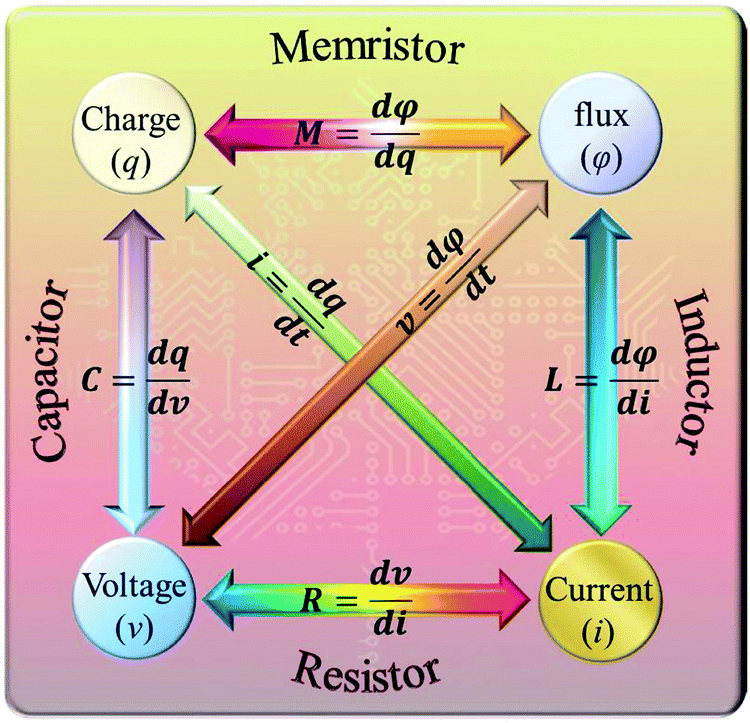 | ||
| Fig. 1 The relationship among four basic circuit variables: voltage (v), current (i), charge (q), and magnetic flux (φ). | ||
Resistance random access memory (RRAM) based on the memristive effect is considered to be the most promising next-generation data storage technology because it can break through the physical limitations of traditional memory devices.11–15 The RRAM can achieve higher storage density, smaller storage unit volume, lower power consumption, faster reading and writing speed and other advantages compared with other existing memories. In particular, the memristor unit can ideally simulate the function of a biological synapse, as shown in Fig. 2. The top electrode (TE) and the bottom electrode (BE) of the memristive unit are just like the pre- and post-synaptic neurons, the carriers (ions or electrons) in the active material are like neurotransmitters, and the flow of electrical signals in the memristor unit is similar to the transmission of biological signals between neurons. Thus, the cross bar array based on the RRAM device structure could be beneficial to the integration of synaptic devices for complicated neuromorphic computing functions because the RRAM shares the same dynamics with the synapse.16–18 For these reasons, the neuromorphic computing realized by memristive devices for artificial intelligence applications has attracted the attention of many researchers.19–25 The hardware realization of this biological synapse function is also an important factor in promoting the development of robots. Therefore, the study of the memristive effect has become a current research focus in materials science, electronics, biology, computer science, etc.26–30
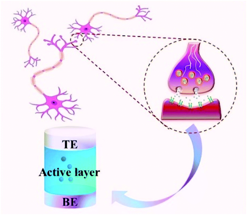 | ||
| Fig. 2 The memristor can simulate the function of biological synapses because the sandwich structure of the memristor unit is similar to nerve synapses. | ||
Compared with other electronic devices, memristors have obvious advantages in material selection and device structure.31–35 In the past ten years, the research on memristive functional materials has made great progress. It has been found that the materials like metal oxide semiconductors, insulators or polymers and biomaterials show a good memristive effect.36–40 In particular, it has also been proved that many perovskite materials have excellent RS effects.4–9 This diversified material selection not only speeds up the research process of the memristive device, but also effectively reduces the manufacturing cost of the device. In this review, we mainly discuss the research progress of the RS effect based on ABO3-type multiferroic perovskite materials, the fabrication method of RS devices, the approaches of building a neural network, and the potential applications of ABO3-type multiferroic perovskite materials in the hardware artificial intelligence systems. The research progress from ABO3-type multiferroic perovskite materials to artificial intelligence is shown in Fig. 3. Finally, we point out the developmental trend and the advanced potential applications of ABO3-type multiferroic perovskite materials based on the RS effect.
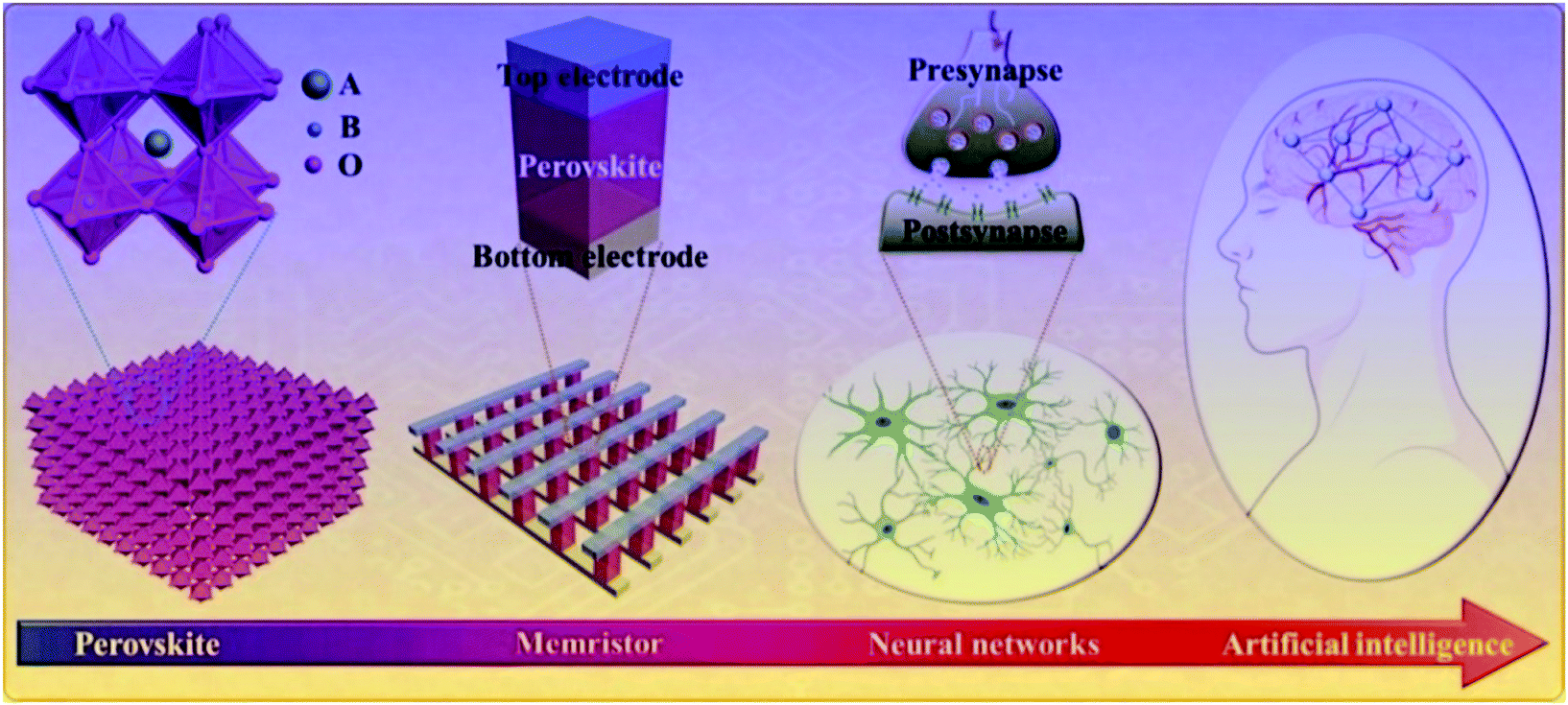 | ||
| Fig. 3 The research progress from ABO3-type multiferroic perovskite materials to the hardware realization of artificial intelligence. | ||
2. ABO3 multiferroic perovskite materials
The multiferroic effect is a phenomenon in which a material with a single or composite-phase exhibits at least two ferroelectric parameters (ferromagnetism, ferroelectricity or ferroelasticity) under certain conditions.41,42Fig. 4a clearly shows the conceptual relationship among multiferroic/ferromagnetic/ferroelectric/ferroelastic properties. Based on the applied considerations, current research mainly focuses on multiferroic materials that simultaneously exhibit both magnetism and ferroelectricity. This type of multiferroic material is also called magnetoelectric material,43–45 which has attracted the attention of researchers from the fields of physical and materials science, and it is expected to develop multistate memory devices due to the magnetoelectric coupling effect.46–48Fig. 4b shows the conceptual relationship among magnetoelectric coupling/ferromagnetism/ferroelectricity, which clearly displays their concept range and the corresponding hysteresis curves. Among the discovered single-phase multiferroic/magnetoelectric materials, it is generally considered that the most practically promising multiferroic materials are TbMnO3 and BiFeO3.49,50 Besides, the development of composite multiferroic materials has played a good supplement to the application of multiferroic materials.51,52 It is well known that material composite technology can combine a variety of nanoparticles of materials with different properties through physical or chemical methods. It is a commonly used material synthesis and processing approach. Therefore, the material composite technology also shows strong effectiveness in the preparation of composite multiferroic materials.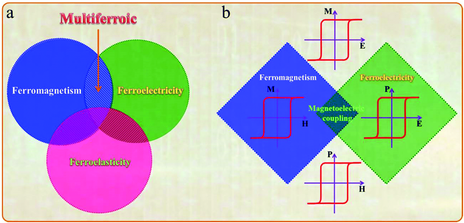 | ||
| Fig. 4 (a) The relationship among multiferroic/ferromagnetic/ferroelectric/ferroelastic materials clearly shows their concept range. (b) The relationship among magnetoelectric coupling/ferromagnetism/ferroelectricity clearly shows their concept range and the corresponding hysteresis curves. | ||
In fact, the concept of multiferroic materials was proposed as early as 1994. Subsequently, several new physical phenomena were triggered due to the special physical properties of multiferroic materials. For example, the magnetoelectric coupling effect can induce a new ferroelectric polarization in a magnetic field or a new ferromagnetic magnetization in an electric field. At present, multiferroic materials have become a research focus in the field of materials science. It should be noted that N. A. Spaldin and R. Ramesh have summarized the multiferroic family tree based on recent development of multiferroic materials,43 as shown in Fig. 5. This figure gives us an intuitive understanding of the evolution of multiferroic materials, including single-phase and composite multiferroic materials. It can be seen that the four roots of the multiferroic family tree combine and interweave in various complicated ways to organize the branches. The most obvious strategies for engineering new multiferroics are to combine one magnetic and one ferroelectric mechanism from these roots to make new branches in this tree. With the continuous discovery of new multiferroic materials, the multiferroic family tree will also grow new branches, and the application of multiferroic materials will also make rapid progress. It is expected to realize a new generation of multifunctional devices, such as new magnetoelectric sensors, spintronic devices, multistate memory devices, etc.53–62
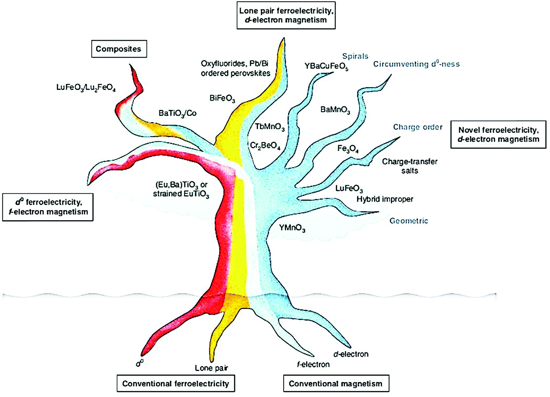 | ||
| Fig. 5 The schematic diagram of the multiferroic family tree, which shows the mechanism of different types of multiferroic materials due to different combinations. Reproduced with permission.43 Copyright 2019, Nature Publishing Group. | ||
Among the well-known multiferroic materials, BiFeO3 and TbMnO3 remain as the most seriously arguable.63,64 The room temperature crystal structure of BiFeO3 is shown in Fig. 6. The displacement of these cations corresponds to the distortion of the ferroelectric phase, and the tilt of the octahedron is usually called the distortion rotation of the antiferromagnetic state. When the rotation direction of the adjacent oxygen octahedra along the crystal direction is reversed, it means the reverse of the antiferroelastic displacement and deformation, and the residual magnetization moment deviates from the b-axis direction at this time.65 In fact, the change of the bond length plays a vital role in the stability of the ferroelectric phase. Based on the changeable structure of BiFeO3, it can exhibit many special physical properties.
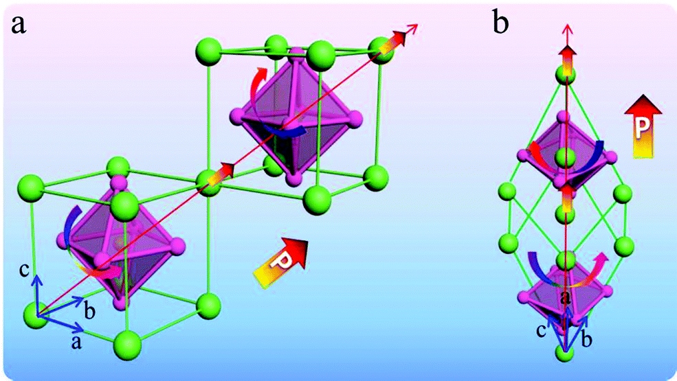 | ||
| Fig. 6 (a) Pseudocubic unit cell including one unit cell. (b) Rhombohedral unit cell including two unit cells. | ||
In particular, BiFeO3 as a typical ABO3 type multiferroic perovskite material has been widely studied with respect to photovoltaic, photoelectric, and magnetoelectric coupling effects,66,67 as shown in Fig. 7. Such multiple properties make BiFeO3 a potential candidate to realize multifunctional devices. BiFeO3 has a typical tripartite structure at room temperature, and its space group belongs to R3c. The ferroelectricity of the BiFeO3 crystal is caused by the lone pair of electrons from the Bi ion. At the same time, BiFeO3 has a G-type antiferromagnetic and spatially modulated magnetic structure. At present, there are many methods for preparing BiFeO3, such as the sintering method, sol–gel method, hydrothermal method, etc.66,67
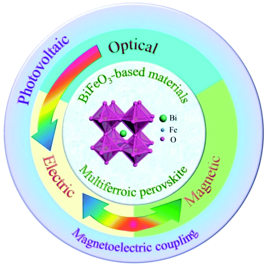 | ||
| Fig. 7 The multiferroic BiFeO3 single crystal material has good photovoltaic, ferroelectric and magnetic properties. | ||
In addition, other perovskite materials with multiferroic properties have attracted the attention of many researchers.68–70 For example, the multiferroic TbMnO3 has an orthogonal perovskite structure, which not only shows good multiferroicity, but also excellent optical properties.43 Thus, TbMnO3 is also a multifunctional material with ferroelectric, ferromagnetic and optical properties. Next, we will discuss the research progress of the RS effect and potential applications in artificial intelligence systems based on these ABO3-type multiferroic perovskite materials.
3. RS effect of ABO3 multiferroic perovskite materials
3.1 Research progress
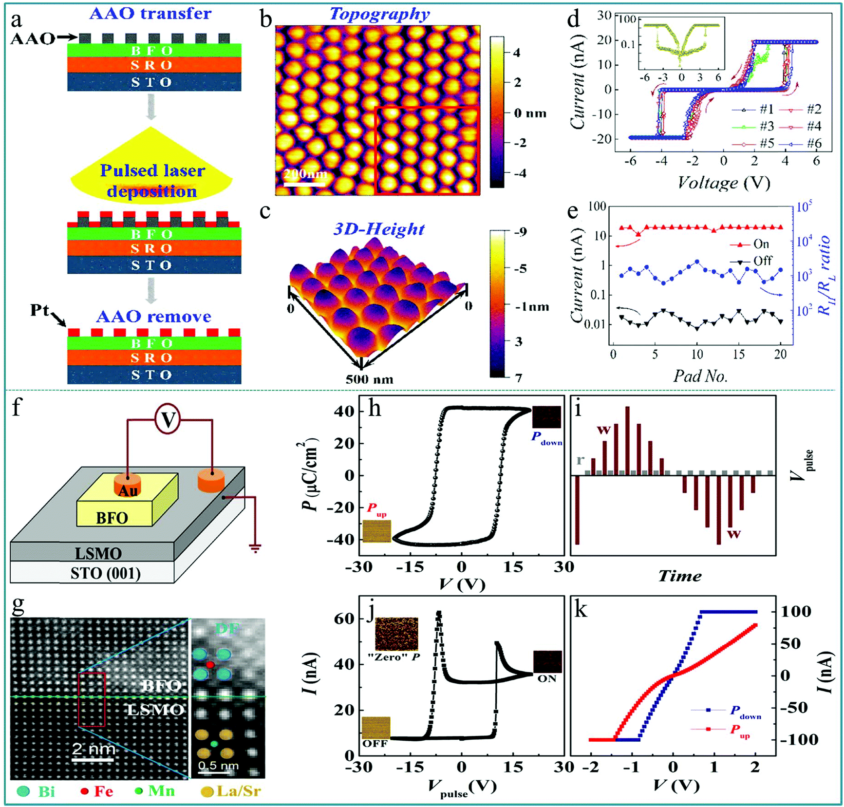
Utilizing the ferroelectric polarization to modify the electron transfer in an ABO3-type function layer, a self-rectifying RS memory behaviour, which was desired for the ultra-large memristor array integration because the sneak current could be suppressed by this self-rectifying effect, was firstly observed in a BiFeO3-based device.71 During the experimental process, a highly oriented ferroelectric BiFeO3 nano-islands array was prepared using a thin anodic aluminum oxide (AAO) nano-template on single-crystal SrRuO3/SrTiO3 (100) substrates by the pulsed laser deposition (PLD) technique. The preparation process is shown in Fig. 8a. In order to deeply explore the polarization-related charge conduction process of BiFeO3 nano-islands, the periodic current–voltage (I–V) characteristics by conductive atomic force microscopy (CAFM) during piezo-response force microscopy (PFM) on BiFeO3/SrRuO3/SrTiO3 nano-islands were simultaneously measured. The schematic of the experimental measurement is shown in the inset of Fig. 8b. In the process of testing, an atomic force microscopy (AFM) tip coated with conductive Pt/Ir acts as the top electrode of the device and SrRuO3 acts directly as the bottom electrode. Thus, this structure constitutes a typical sandwich device. The I–V measurements were carried out repeatedly by sweeping the applied voltage in the sequence of 0 → 3.5 V → −3.5 V → 0 V. One can clearly observe a large hysteresis behavior in the I–V curve in Fig. 8b, reflecting the existence of a RS effect. Besides, the comparison between PFM amplitude/phase images and the obtained I–V curve in the low voltage region of ±1.5 V below transition voltages confirmed that the ferroelectric polarization reversal induced transitions of the forward-direction, and thus the down- and up-polarizations were accompanied by positive- and negative-forward, respectively, as shown in Fig. 8c. Taking into account the self-rectifying RS effect, low SET/RESET current and nanoscale cell size, the BiFeO3-based memristor exhibits great potential application in the neuromorphic computing system with low power consumption, reliable computing accuracy and considerable hashrate.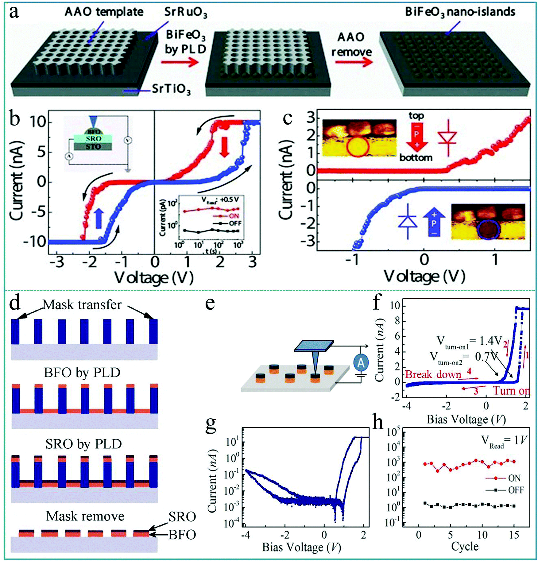 | ||
| Fig. 8 (a) Fabrication process of the BiFeO3 nano-islands array; (b) I–V curves of the Pt/BiFeO3/SrRuO3/SrTiO3 device demonstrate the switchable ferroelectric diode effect in the voltage range of ±3.5 V; (c) I–V curves measured on a single BiFeO3 nano-island at down-polarization (positive-forward diode) and up-polarization (negative-forward diode) states below the coercive voltage, respectively. Panels a–c reproduced with permission.71 Copyright 2013, Wiley-VCH. (d) Schematic flow chart illustrating the fabrication procedure of the BiFeO3/SrRuO3 nanocapacitor arrays on a Nb-doped SrTiO3 substrate. (e) The schematic diagram of the device measurement. (f) Local I–V curves show both a large rectification and a RS behavior at a maximum bias voltage of 4.0 V. (g) The replotted I–V curve in a semi-logarithmic form. (h) The endurance test with 15 cycles under a readout voltage of 1.0 V. Panels d–h reproduced with permission.72 Copyright 2015, Nature Publishing Group. | ||
In previous reports, the preparation of nanomaterials using AAO nano-templates has shown many advantages, such as uniform distribution, good orientation, and controllable size and density.73–76 The AAO template can usually be prepared by an electrochemical corrosion process, which has the advantage of being simple and easy to implement, and size of the hole diameter can be adjusted according to different experimental requirements. Currently, AAO templates have a wide range of applications in nano-assembly systems, including the assembly of quantum dots, nanowires, nanotubes, and “coaxial cable type” layered nanowire materials. Their use not only simplifies the preparation process of nanomaterials, but also provides good feasibility for industrialized production.
The method of preparing nanodevices using AAO templates has been adopted by many researchers. Lina Zhao et al. prepared well-ordered multiferroic BiFeO3 nanocapacitor arrays on conductive Nb-doped SrTiO3 (Nb-STO) substrates by a combination of PLD method and AAO template.72 After the deposition was completed, the removal of the AAO template depends on its ability to be easily dissolved in acidic solutions. Then, an apparent current-rectification effect and RS behavior in the sandwich structure cells consisting of BiFeO3/SrRuO3 (BFO/SRO) heterostructure nanodots have been observed. The RS device was obtained after four production steps, as illustrated in Fig. 8d. To further examine the RS memory behavior, the I–V characteristics of a single BiFeO3 nanodot were tested by using the CAFM tip as the top electrode and Nb-STO as the bottom electrode of the device. The schematic structure of the device is depicted in Fig. 8e. A hysteresis behavior in the I–V curve can be observed in Fig. 8f, indicating an apparent RS effect with an obvious rectification property. Fig. 8g shows the corresponding non-zero-crossing I–V curve based on logarithmic coordinates, indicating that a polarized internal electric field caused by the ferroelectric polarization effect was generated under an external electric field. Finally, to examine the stability of the RS behavior, the I–V sweeps with 15 cycles under a reading bias of 4.0 V were performed. The ON/OFF currents at a reading voltage of 1.0 V are plotted in Fig. 8h, showing that the device has almost no attenuation after 15 successive cycles. These experimental results indicate that the multiferroic BiFeO3 nanodot arrays offer potential possibilities to utilize these simple sandwich structure arrays in high-density nonvolatile RRAM memories and other multifunctional nano-electronic devices.
Similar to the preparation method of the device in the above works, Zengxing Lu et al. prepared well-ordered and high-density isolated Pt nano electrode arrays on BiFeO3 (BFO) ultrathin films grown on a SrTiO3 substrate using the AAO nano-template, and observed a good ferroelectric RS characteristic.77 The fabrication processes of the Pt/BiFeO3/SrRuO3 device are shown in Fig. 9a. The nanocapacitor arrays are well-ordered, and the diameter of Pt nano electrodes observed from Fig. 9b is ∼60 nm. The thickness of Pt nano electrodes is ∼8 nm (Fig. 9c). Thus, the volume of each device unit is very small. The I–V hysteresis loops were measured using the sweeping applied voltage with a sequence of 0 → 6.0 V→ 0 → −6.0 V→ 0, as shown in Fig. 9d, showing a stable RS performance. It should be noted that there is a relatively small output current. This kind of device can be used in electronic devices requiring a small current. The corresponding I–V curve in a logarithmic form is shown in the inset of Fig. 9d, in which we can see that this I–V curve is almost completely symmetrical even though the structure of the device is asymmetrical. In particular, this device has a very large resistance window of approximately 103. This large resistance window provides the possibility for high-density information storage. Fig. 9e shows that the ON/OFF current values only slightly deviate with the increasing number of cycles, indicating the good reproducibility of the RS behavior in the Pt/BiFeO3/SrRuO3 device. These results suggest that the BiFeO3 ultrathin film-based nanocapacitors are promising candidates for nonvolatile ferroelectric RS memories with a small output current and ultrahigh integrated density. In addition, the use of AAO templates provides a reliable way for the preparation of high-density integrated RS memory devices. Furthermore, this preparation method using AAO template associated pulsed laser deposition is simple and easy to implement during the actual experiment, and thus it is easy for large-scale industrial production.
 | ||
| Fig. 9 (a) Schematic flowchart illustrating the procedures of fabricating the Pt/BiFeO3/SrRuO3 nanocapacitor arrays on a SrTiO3 substrate; (b) 2D and (c) 3D topography images of the Pt nanodots; (d) I–V hysteresis loops measured for multiple cycles, and the inset shows the I–V hysteresis loop plotted on a semilogarithmic scale; (e) RS parameters measured for different nano capacitors. Panels a–e reproduced with permission.77 Copyright 2016, American Chemical Society. (f) Schematic illustration of the measurement configuration of the sample; (g) typical STEM-HAADF image of the BiFeO3/La0.6Sr0.4MnO3 interface showing the good epitaxial properties of the heterostructure; (h) remnant P–V hysteresis loop of the heterostructure with f = 5 kHz at room temperature; (i) schematic pulse train for the I–V pulse loop; (j) steady-state current measured as a function of 100 μs writing pulses using the pulse train shown in part (i); the corresponding domain structures measured by the out of plane piezoelectric AFM are shown in the middle right, bottom left, and top left insets for the LRS (ON), HRS (OFF), and zero polarized states, respectively; (k) I–V curves measured after applying Vp = ±20 V. Panels f–k reproduced with permission.78 Copyright 2015, American Chemical Society. | ||
Furthermore, Lei Feng et al. investigated the ferroelectric RS effects of the Au/BiFeO3/La0.6Sr0.4MnO3 (Au/BFO/LSMO) multiferroic heterostructure on a SrTiO3 (001) single crystal substrate,78 in which the Au top electrode with a diameter of 0.3 mm was sputtered on the BiFeO3 thin film, as shown in Fig. 9f. For testing of the RS properties, the traditional current perpendicular to the film plane was employed, and the forward bias was defined as a positive voltage applied to the device unit. The cross section STEM-HAADF image of the interface of the BiFeO3/La0.6Sr0.4MnO3 heterostructure by scanning transmission electron microscopy (STEM) using a high angle annular dark field (HAADF) detector is illustrated in Fig. 9g, in which the position of the BiFeO3/La0.6Sr0.4MnO3 interface is labeled by a green line. The room temperature ferroelectric hysteresis loop (P–V) at 5 kHz is shown in Fig. 9h. It exhibits a large coercive force and residual ferroelectric polarization, and no leakage current is observed. To study the RS behaviors of the heterostructure, the I–V pulse is measured with the testing pulses composed of a series of write-pulses (0 V → 20.0 V → −20.0 V → 0 V) with different amplitudes and a read-pulse (0.3 V) following each write-pulse as shown in Fig. 9i. With the heterostructure prepolarized upward by a pulse (amplitude: −20.0 V), the nonvolatile RS phenomenon of the heterostructure is demonstrated by the clear hysteretic I–V curve (Fig. 9j). To investigate the origin of the low resistance state (LRS) or “ON” state and the high resistance state (HRS) or “OFF” state, the I–V curves at the fully downward and upward polarization states were further measured, as shown in Fig. 9k, in which a standard bipolar RS behavior with a clear HRS (red line) and LRS (dark blue line) was observed, which is relative to the upward polarization and downward polarization of the device. In a word, the above findings are helpful for us to understand the effects of interfaces and the ferromagnetism of ferroelectric domain walls (DWs) in multiferroic heterostructures on the nonvolatile RS characteristics. This interface coupling is directly related to the electron spin coupling by ferroelectric polarization. Therefore, this work may give a possibility for combining the RS device with spintronics. In fact, many devices based on the spin of electrons and molecules have been developed, such as spin diodes and spin photovoltaic devices. They have completely new device functions that are extremely different from those of traditional electronic devices. Such devices might have great potential applications in spintronics.
It is well known that the ferroelectric properties of ferroelectric materials originate from the spontaneous polarization of electrons in the ferroelectric domains,79 and the spontaneous magnetization of electrons in the magnetic domains makes the material exhibit magnetism.80 Therefore, the macroscopic performance of multiferroic materials comes from the rotation or movement of microscopic ferroelectric domains and magnetic domains. In addition, molecular electronics uses functional molecular materials to construct various electronic components in circuits, such as molecular wires, switches, diodes, field effect transistors, memory devices, etc.81–85 The target of studying molecular electronic devices is to use single molecules, supramolecules or molecular clusters to replace silicon-based semiconductor transistors and other solid electronic components to assemble logic circuits. In particular, the molecules of ferroelectric materials are rearranged under the action of an externally applied voltage, so that the polarization moment of ferroelectric polarization in a certain direction in the crystal is not equal to zero, thereby presenting a polarized electric field in that direction.86–88 Molecular memory devices are the basic memory element of all electronic devices, which is also an important part of molecular storage and logic devices. Therefore, molecular memory devices are becoming an important research direction for the development of electronic devices in the future.
Electron-type RS behaviour featured by continuous SET/RESET process enables the neuromorphic computing system with high computing precision and avoids the conductance clamping, thus, it is favorable to establish the electron-type RS system by controlling the proportion of charged domain walls in the ferroelectric or ferromagnetic ABO3 perovskites. The reversible RS behavior between stable, nanoscale, strongly charged domain walls (sCDWs) and the corresponding nano domains in an epitaxial BiFeO3 (BFO) thin film was reported by Xiaoqing Pan's group.89 In this research, the RS was performed upon 20 nm thick (001)P oriented BFO single crystalline films. A bias was applied between a tungsten surface probe and the La0.7Sr0.3MnO3 (LSMO) bottom electrode (Fig. 10a). Fig. 10a presents a schematic diagram of the change of the domain walls (DWs) in the functional layer corresponding to the writing and erasing processes. Interestingly, the bulk domains possess a rhombohedral-like perovskite structure with polarization pointing along the body diagonal of the BiFeO3 lattice (Fig. 10b). The polarization near the strongly charged domain wall has rotated in the direction normal to the BFO/LSMO interface, which can form a tetragonal-like perovskite structure. This structural change was also reproduced by phase-field simulation of the sCDWs’ configuration although the sCDW was inclined (Fig. 10c). On the other hand, the system can be stable without a sCDW under the simulated result (Fig. 10d). This work indicates that the ultrahigh-density information storage can be realized based on the sCDW, which has laid a good experimental foundation for the development of multifunctional molecular memory devices based on multiferroic perovskite materials.
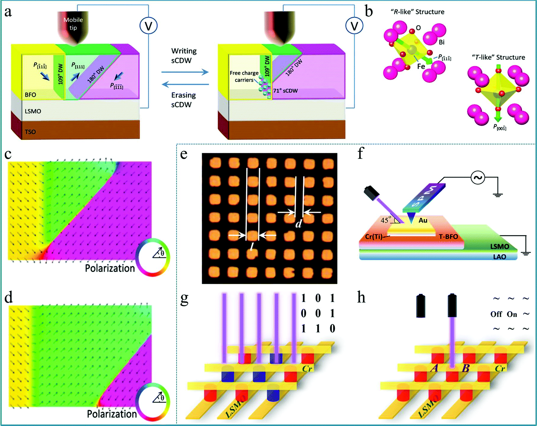 | ||
| Fig. 10 (a) Schematic of the experimental set-up; (b) atomic models of the R-like structure of the domains and the T-like structure of the sCDW in BiFeO3, in which the polarizations are shown by green arrows; (c) phase-field simulation of the polarization distribution in the plane of the image of the stable domain structure with a sCDW in a BiFeO3 film; (d) simulated polarization distribution in the plane of the image of the stable domain structure of the system without a sCDW where the arrows mark the polarization orientations. Panels a–d reproduced with permission.89 Copyright 2016, Wiley-VCH. (e) Optical image of the microarray derived from Au/Ti (or Cr)/T-BFO/LSMO, in which the side length of each square electrode is l = 2.5, 5, 10, and 20 μm and the gap between the squares is d = 1.5, 5, 5, and 5 μm; (f) setup for measuring the local photovoltaic effect; (g) data storage and (h) logic switching microdevice prototype designed based on the Au/Cr/T-BFO/LSMO microarray. The yellow bars represent electrodes (LSMO and Cr); the red and blue columns represent the Pdown state and Pup state, respectively, of the T-BFO films. Panels e–h reproduced with permission.90 Copyright 2017, American Chemical Society. | ||
Based on the aforementioned research on tetragonal-like perovskite BiFeO3 (T-BFO), the photoelectric properties of multiferroic materials have attracted widespread attention. In particular, the photovoltaic effect of BiFeO3 shows its unique potential applications.91 Since the bandgap width of BiFeO3 is about 2.0–3.0 eV, BiFeO3 is expected to achieve good visible light photovoltaic and photocatalytic effects, suggesting that BiFeO3 can be used in the research of solar water splitting to produce hydrogen. Thus, BiFeO3 has good application prospects in the preparation of new energy.92–94 In previous reports, it was generally believed that the photovoltaic effect of BiFeO3 is attributed to the interface energy barrier (interface effect), ferroelectric polarization (body effect), and the defect concentration gradient under an applied electric field.95 In order to better present these effects, a single crystal film prepared by the epitaxy method is crucial. A typical experiment should be mentioned in which a well-ordered microarray of epitaxial tetragonal BiFeO3 (T-BFO) films on the single-crystal (001)-LaAlO3 substrate with a 10 nm thick La0.67Sr0.33MnO3 (LSMO) buffer layer was deposited by PLD.90 This single-crystal (001)-LaAlO3 substrate provides a key factor for the preparation of single-crystal T-BFO films. In the micro-array, each cell was designed as a square with various side lengths and gap widths, as shown in Fig. 10e. To study the ferroelectric photovoltaic effect of the Au/Cr(Ti)/T-BFO/LSMO structure, a combined measurement system integrating a scan probe microscope (SPM) was used, as sketched in Fig. 10f. The rapid photovoltaic response to incident light provides a feasible way to develop a unique technology for information memory and logical computing. In order to build an array of memory devices, a sandwich structure based on the Au/Cr/T-BFO/LSMO microarray was proposed, as shown in Fig. 10g. Each intersection of the device represents a logic state, which can achieve good information processing through logic operations. In addition, a RS device using the presented tunable ferroelectric photovoltaic effect of Au/Cr/T-BFO/LSMO was also developed, as shown in Fig. 10h. For a given cell (such as B device unit) with the Pdown state, its logic state can be reversibly switched between the ON and OFF states by controlling the incident laser, and then it can be read out by detecting the corresponding VOC (JSC). Therefore, this work is greatly meaningful for deeply understanding the photovoltaic process of BiFeO3-based devices at the microscale and provides a feasible approach for developing information memory and in-memory devices using the ferroelectric photovoltaic effect.
In addition to BiFeO3, BaTiO3 was also reported as an important multiferroic material in the ABO3 system with a wide range of applications.96–100 BaTiO3 has a large dielectric constant and a small dielectric loss, and it is one of the widely used materials in electronic insulating ceramic materials. The spontaneous polarization of BaTiO3 mainly comes from the ion displacement polarization of Ti4+ and the electron displacement polarization of O2−. In the field of ceramics, BaTiO3 is mainly used as an insulation layer in electronic ceramics, thermistors, capacitors, electronic components, and in the reinforcement of some composite materials. Furthermore, the multiferroic perovskite-type BaTiO3 has also been used in energy storage and catalysis research,101–105 and it can present more characteristics through element doping. BaTiO3 as one of the important members of the ABO3 family also exhibits great potential application in the neuromorphic computing system because its spontaneous polarization features are possibly used to simulate the physical biodynamic process.
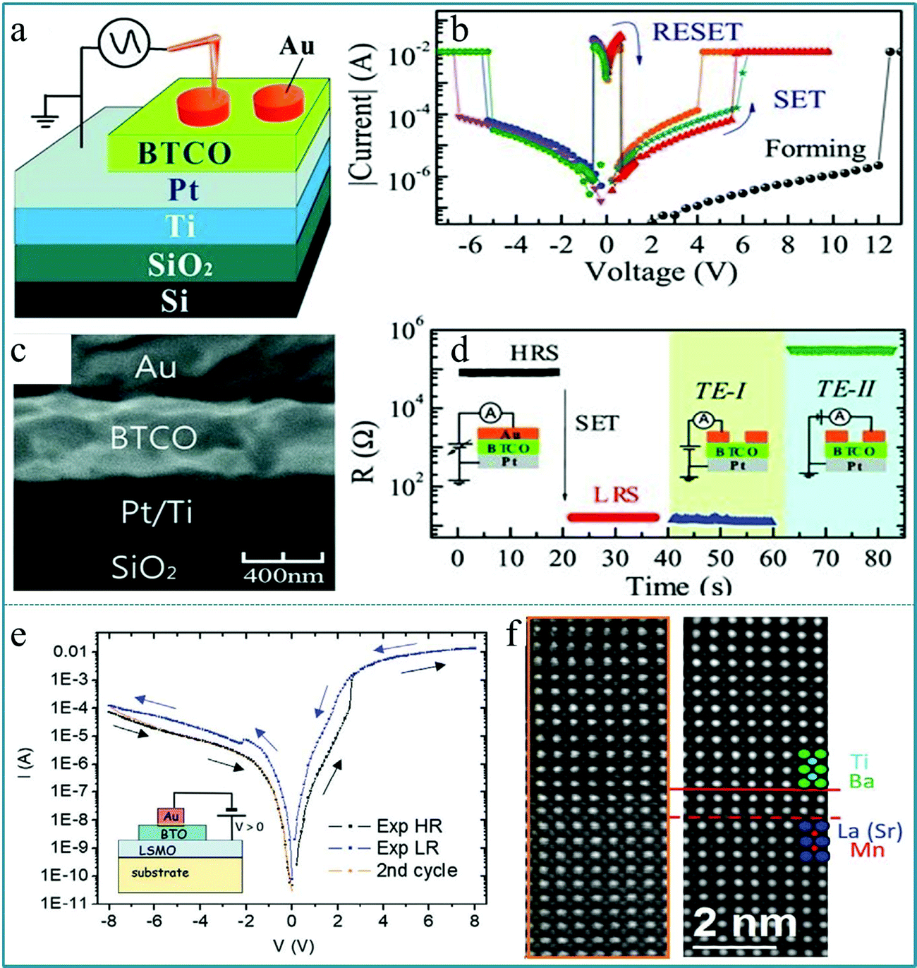
Zhibo Yan et al. fabricated a RS memory device using 5 at% Co-doped BaTiO3 (BTCO) as a functional layer, which demonstrated a unipolar RS characteristic.106Fig. 11a depicts a schematic drawing of the measurement configuration, in which Au works as the top electrode and Pt works as the bottom electrode. Fig. 11b shows the typical I–V characteristics of the memory cell, displaying an obvious set and reset process appearing in the same voltage area (positive voltage region or negative voltage region), which is confirmed as a unipolar RS effect. The SEM image of the cross-sectional profile of the as-prepared BTCO thin film is shown in Fig. 11c, showing that the thickness of the BTCO layer is ∼400 nm. Finally, to verify the inhomogeneous conduction of the memory cell and therein the filament model, an Au top electrode was prepared to set the memory cell into the LRS, then the electrode was cut into two parts (TE-I and TE-II) using the probe tip, and the resistances between the bottom electrode and TE-I or TE-II were measured, as shown in Fig. 11d. It shows multiple logic states by selecting contacts with different electrodes. The data obtained above confirm that the multiferroic perovskite BaTiO3 can offer a good opportunity for developing RRAM devices with more promising functionalities. Furthermore, Nathalie Jedrecy et al. prepared a RS device based on the multiferroic BaTiO3/La0.75Sr0.25MnO3 (BTO/LSMO) system.107 The hysteretic I–V curves of the Au/BTO/LSMO structure show an obvious bipolar RS behavior, as shown in Fig. 11e. It can be confirmed that Ba and Ti ions in LSMO are diffused from the observation of the high-resolution STEM image in Fig. 11f. Therefore, this study confirmed the important role of ion exchange and redox processes in the heterojunction interface in RS devices.
 | ||
| Fig. 11 (a) A schematic drawing of the measurement configuration; (b) typical I–V characteristics of the device; (c) cross-sectional SEM image of a memory cell; (d) resistances measured for various configurations, in which the top electrode (TE) was cut into TE-I and TE-II by the probe tip after the cell was switched from a HRS to a LRS. Panels a–d reproduced with permission.106 Copyright 2011, Wiley-VCH. (e) The I–V hysteresis curve in a logarithmic form, and the inset shows the Au/BTO/LSMO structure; (f) the high resolution raw (left) and filtered (right) STEM images. Panels e and f reproduced with permission.107 Copyright 2021, Wiley-VCH. | ||
At present, the perovskite-type LaMnO3 is used for various energy storage and magnetic devices, and has become a widely studied functional material.108–113 LaMnO3 is a typical ferromagnetic material, and it has a wide range of applications in spin valves, magnetic read heads and exchange bias devices.114–117 In particular, LaMnO3 exhibits a good exchange bias dependence on direction in a heterojunction superlattice.118 These characteristics make LaMnO3 an advanced functional material in the preparation of spintronic devices. The ferromagnetic property originating from LaMnO3 endows the LaMnO3-based memristor with enriched spin electron effects, such as electron spin transport, coupling and resonance. Utilizing these advantages, the RS behaviours elaborately modulated by signal parameters (voltage magnitude) in a computing system can efficiently simplify the external circuit, and thus cutoff the hardware cost.
It should be mentioned that Andrés Gómez et al. prepared a RS device with BaTiO3−δ/La0.7Sr0.3MnO3/SrTiO3/Si structure by a relatively complicated process and measured the RS characteristics.119 It was found that the ferroelectric polarization can be reversed upon a mechanical load in the as-prepared RS device. Thus, a mechanically controlled multilevel device was further designed. Fig. 12a shows the complex epitaxial heterostructures grown in three different stages. The SEM image confirms this multi-layer structure device (Fig. 12b). The measurements of electron energy-loss spectroscopy (EELS) with atomic resolution shows some cation intermixing is restricted in the interface, which is in agreement with the contrast, as shown in Fig. 12c. This special interface is usually an important factor for heterojunction devices. Next, the charge transport and RS behavior of the BaTiO3−δ film were investigated. The test configuration is shown in Fig. 12d, in which the CAFM tip works as the top electrode and La0.7Sr0.3MnO3 works as the bottom electrode. By setting a bias voltage of −6.0 V on the La0.7Sr0.3MnO3 bottom electrode, the device was set into a LRS while a +6.0 V bias switched the device to a HRS (Fig. 12e), implying that a bipolar RS effect with obvious asymmetry can be implemented in the as-fabricated RS device. Fig. 12f shows the mapping diagram of the BaTiO3 film with a thickness of 45 nm. It can be seen that the RS device can be driven by electric polarization (right) and mechanical loading force (left), and the resistance state can be changed between LRS and HRS. Finally, the authors summarize the configurations in which the system can be switched internally between HRS and LRS upon application of those external stimuli.119 Therefore, this work indicates that perovskite-type heterojunctions have great potential applications in multistate RS devices due to the special performance of the interface layer, which provides an innovative pathway toward the design and integration of nonvolatile mechanoelectrically controlled multilevel RS devices. The mechanoelectrical RS performance has potential applications in information memory and sensor applications.
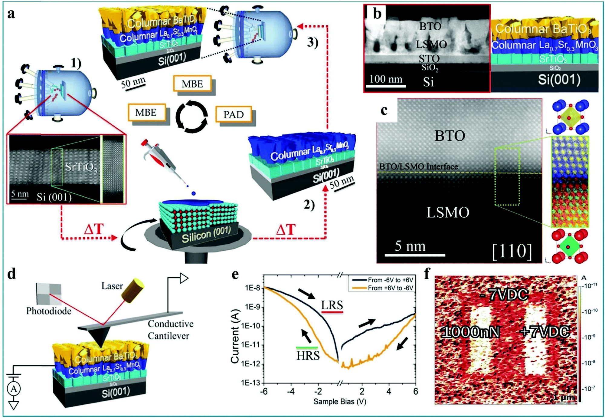 | ||
| Fig. 12 (a) Schematic diagram illustrating a new preparation approach combining molecular beam epitaxy (MBE) and polymer assisted deposition (PAD). (b) Low magnification Z-contrast image of a porous epitaxial BaTiO3−δ/La0.7Sr0.3MnO3/SrTiO3/Si (001) multilayer along the [110] Si axis (left panel), corresponding to the sketch of the heterostructure (right panel). (c) High resolution Z-contrast image of the BaTiO3−δ/La0.7Sr0.3MnO3 interface (yellow dashed line) along the Si [110]-crystallographic direction, and higher resolution Z-contrast image of the coherent interface between BaTiO3−δ and La0.7Sr0.3MnO3 layers. (d) Schematic of the CAFM system used for nanoscale electrical measurements. (e) The bipolar RS characteristic of epitaxial columnar BaTiO3−δ/La0.7Sr0.3MnO3/SrTiO3/Si (001) films. (f) Mapping of the electrical current of the 45 nm thick BaTiO3 film shows the piezo-driven RS effect between a LRS and a HRS domain by electrical poling (right) and mechanical loading force (left). All panels reproduced with permission.119 Copyright 2017, Wiley-VCH. | ||
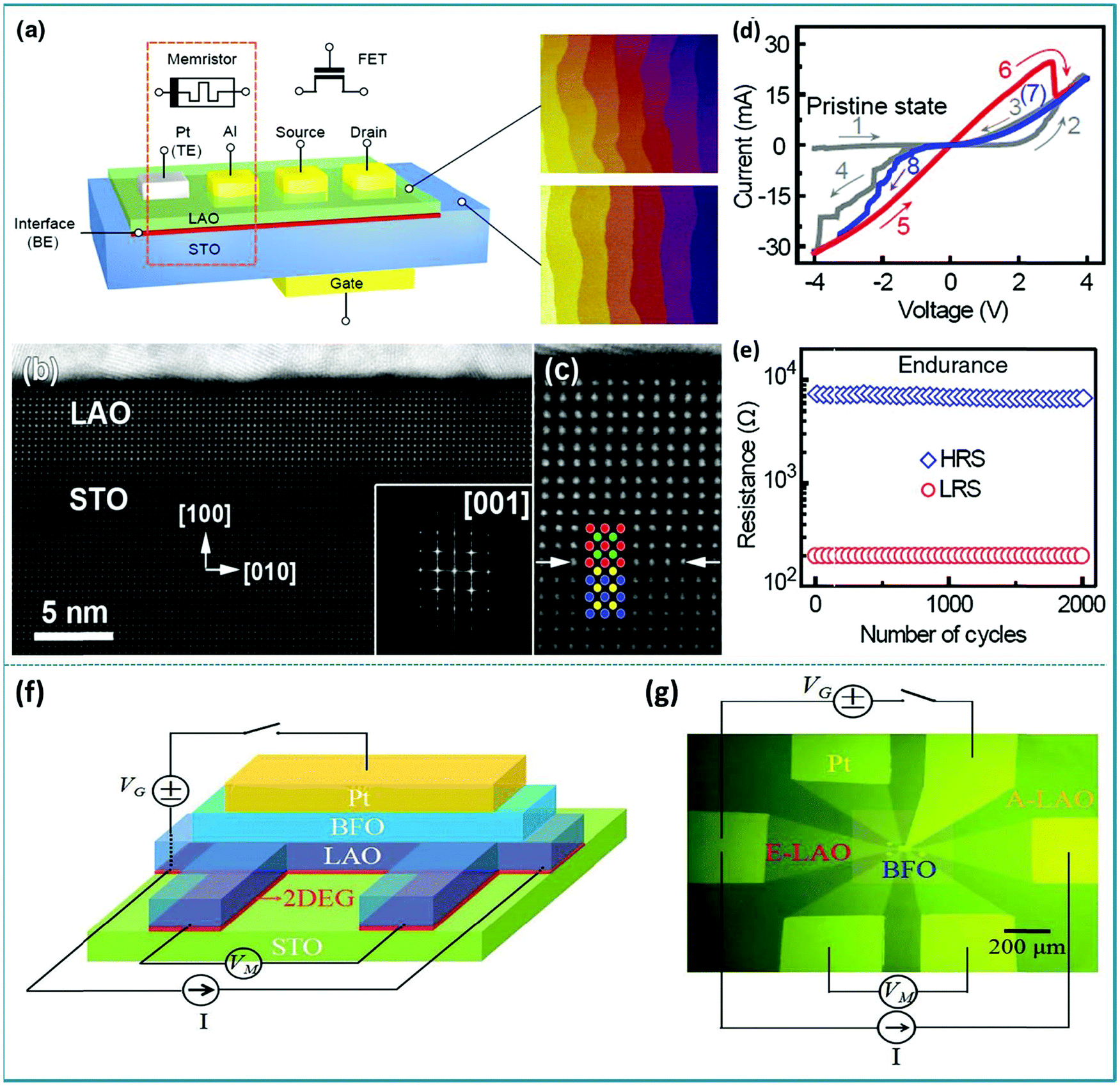
SrTiO3 (STO) is one of the most extensively studied perovskite materials with multiferroic properties in the family of multiferroic materials, and it exhibits many intriguing physical and chemical properties.120–123 SrTiO3 has very good thermal stability, and thus it can be used in electronic ceramic materials and in the manufacture of diamonds.124–128 SrTiO3 is a center-symmetric paraelectric dielectric material with a perovskite structure at room temperature, and it has a very large dielectric constant at low temperatures.129 In addition, SrTiO3 has a band gap of 3.2 eV and shows good photocatalytic activity.130 Many reports have confirmed that SrTiO3 has unique oxidation–reduction catalytic activity, and it has been widely used in the fields of photocatalytic water splitting to produce hydrogen, photocatalytic degradation, photochemical batteries, and so on.131–133 The SrTiO3-based memristor endowed with both nonvolatile and volatile RS behaviors triggered by the multiferroic-induced phase change exhibits multi-order states, which enables more faithful simulation of the synaptic plasticity.
At present, SrTiO3 also presents many advantages in the research of RS devices.134–136 Hyunsoo Lee et al. demonstrated a bipolar RS device based on Nb-doped SrTiO3.137 During the experiment, the CAFM tip was used to contact the Pt nanodisk electrode on a Nb-doped SrTiO3 (Nb:STO) single crystal under the condition of ultrahigh vacuum. By applying a bias of ±8.0 V on the RS device, the I–V curves were obtained. In the process of testing, silver paste and indium with good conductivity were employed to make Ohmic contact between the Nb:STO single crystal and the bottom electrode, as shown in Fig. 13a. The results suggested that the RS device can be scaled down to the 10 nm range for high-density RRAM devices. In addition, Shuxiang Wu et al. reported a reversible RS behavior in a transparent ITO/LaAlO3/SrTiO3 (ITO/LAO/STO) structure device at room temperature.138 To investigate the RS characteristics, wire-shaped Al electrodes were directly contacted with the electron gas and ITO as a counter electrode, as shown in Fig. 13b. This work shows that the LAO/STO heterostructure-based device features good electronic transparency, a high HRS/LRS resistance ratio, good endurance, and long retention of logic states, and is expected to be used in high-performance information processing technologies.
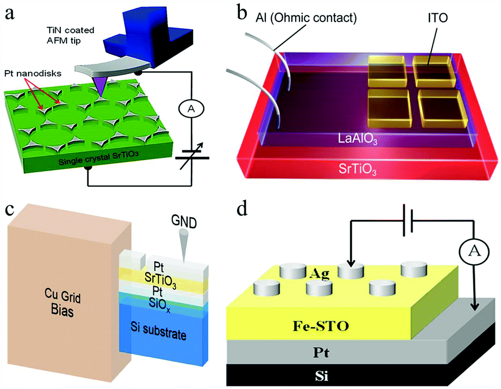 | ||
| Fig. 13 (a) Scheme for nanoscale bipolar RS phenomena on a triangular-shaped Pt nanodisks/Nb:STO single crystal Schottky junction; probing with CAFM in ultrahigh vacuum. Reproduced with permission.137 Copyright 2013, American Chemical Society. (b) Schematic diagram of the transparent ITO/LAO/STO memristor. Reproduced with permission.138 Copyright 2014, American Chemical Society. (c) Schematic of the TEM sample used for in situ I–V experiments. Reproduced with permission.139 Copyright 2019, Wiley-VCH. (d) Schematic diagram of the Ag/Fe-SrTiO3/Pt memory cell. Reproduced with permission.140 Copyright 2020, AIP Publishing. | ||
Further, Deok-Hwang Kwon et al. elucidated the mechanism of filament formation and observed its associated RS effect in a SrTiO3 based special shaped structural device.139Fig. 13c shows a schematic diagram of the structure of the device. In the process of electronic testing, a bias was applied to the bottom electrode while grounding the Pt/Ir-coated W scanning tunneling microscope (STM) tip, which remained in contact with the top electrode of the device. In order to hinder the flow of DC current to the Cu grid through the top electrode, a focused ion beam (FIB) was used to cut off the top electrode near the grid. Thus, this work provides detailed insights into the origin and mechanisms of filament generation and rupture. In addition, many reports confirm that the doping of metal elements can effectively reduce the switching voltage of the device.141,142 Xue Jiang et al. deposited Fe-doped SrTiO3 (Fe-STO) films on a Si substrate by magnetron sputtering to build a RS device with Ag/Fe-STO/Pt structure as illustrated in Fig. 13d, and then investigated the effect of deposition temperature on the RS characteristics.140 It was experimentally observed that the stability of the RS device was significantly improved as the deposition temperature increased. This work indicates that Fe doping can effectively improve the formation of oxygen vacancy conductive filaments in highly crystalline SrTiO3 films, resulting in a small switching voltage for the Ag/Fe-STO/Pt device. Therefore, such devices have potential applications in low-voltage RS memory devices.
More recently, the RS applications of composite multiferroic perovskite oxides, such as SrFeOx, SrTiO3 and La2/3Sr1/3MnO3, have also attracted the attention of researchers.143–145 The structure can change between limonite and perovskite when oxygen ions are diffused.146,147 The memristive effect based on the structural phase change has led to the realization of phase-change memristors. As the name suggests, phase change memory is a kind of RS memory that uses the reversible conversion of conductivity in special materials between the crystalline state and the amorphous state as a logic state to store data. Moreover, phase change memory has the advantages of fast access speed and high reliability, and has broader application space and better developmental trends than other memories. Among all phase change materials studied, the reversible phase transformation between brownmillerite SrCoO2.5 (BM-SCO) and perovskite SrCoO3 (P-SCO) has important potential applications and has received widespread attention. Jie Zhang et al. prepared SrCoO3−δ films by the PLD technique and demonstrated a phase competition under different temperatures.148 The summarization of c-axis lattice constants is shown in Fig. 14a, in which the dashed line indicates the theoretical c-axis lattice constant for the P-SCO film strained on LaAlO3 substrates. In this figure, it can be divided into three areas duo to the c-axis lattice constants compared with the theoretical parameter. Fig. 14b shows the temperature dependent Gibbs free energy of SrCoO2.5 and SrCoO3 by first principles calculations, in which the structure models of SrCoO3 and SrCoO2.5 are displayed in the left and right areas, respectively, and the arrows in the inset schematic diagrams indicate the trend of stabilizing the specific phase structure. Therefore, the conversion between BM-SCO and P-SCO is closely related to a large number of oxygen vacancies.
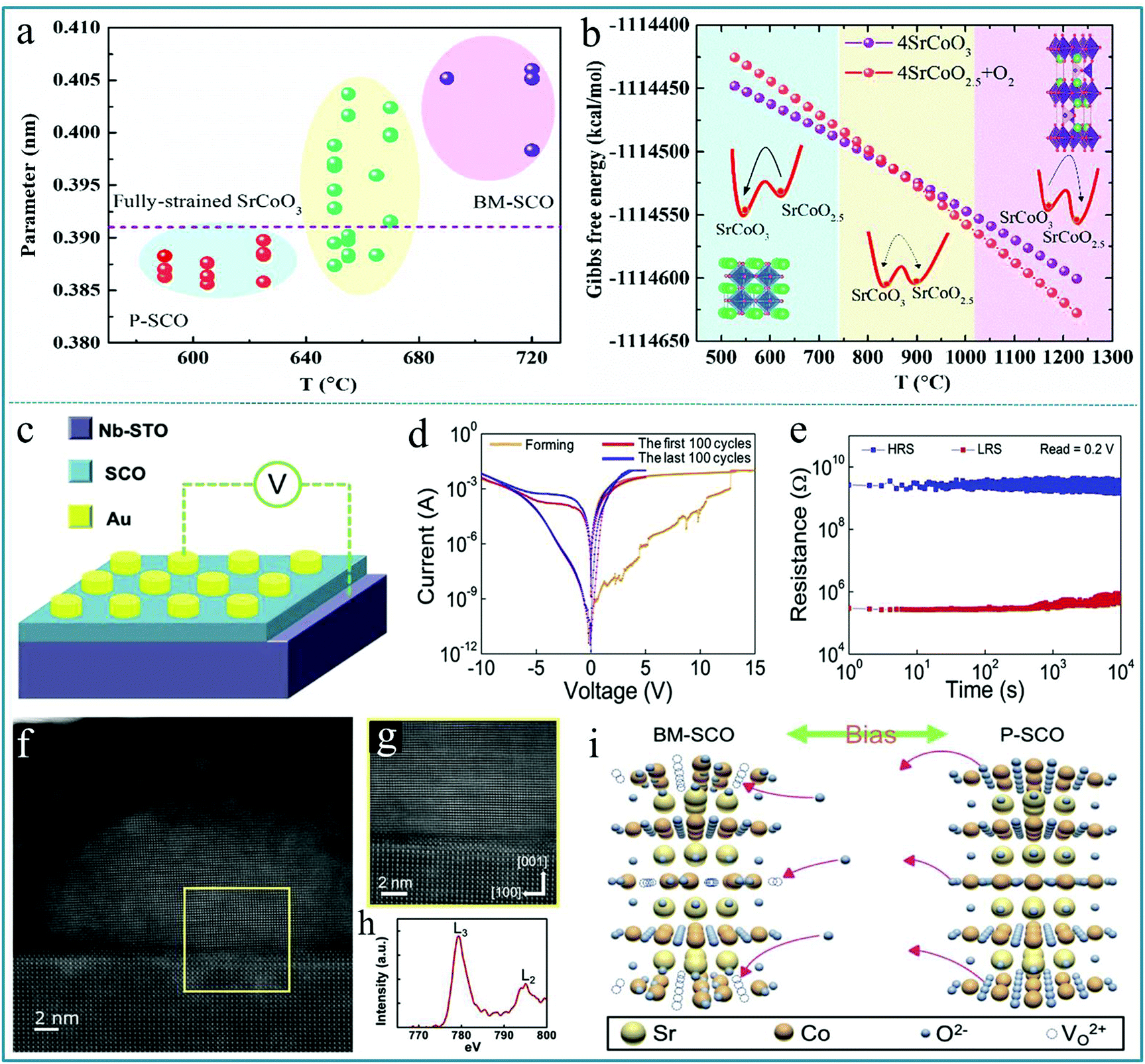 | ||
| Fig. 14 (a) Summarization of c-axis lattice constants; (b) temperature dependent Gibbs free energy of SrCoO2.5 and SrCoO3 by first principles calculations. Panels a and b reproduced with permission.148 Copyright 2020, AIP Publishing. (c) The schematic diagram of devices, in which the bias was applied to the Au electrode and the Nb-STO electrode was grounded; (d) the electrical measurement of the RS behavior shows the typical Forming, Set, and Reset processes where the red and blue curves indicate the first and last 100 cycling tests, respectively; (e) the retention measurement of devices; (f) STEM image of the nanofilament region; (g) HR-STEM image of the interface between the P–SCO nanofilament and the STO electrode; (h) Co L-edge EELS spectrum of the nanofilament region; (i) the schematic diagram of the topotactic phase transformation between BM-SCO and P-SCO. Panels c–i reproduced with permission.149 Copyright 2020, Elsevier. | ||
Hung-Yang Lo et al. deposited SrCoOx (SCO) on a niobium-doped SrTiO3 (Nb-STO) substrate by PLD as the functional layer to prepare a RS device with Au as the top electrode and Nb-STO as the bottom electrode.149 The schematic diagram of the device is shown in Fig. 14c; Fig. 14d shows the obvious bipolar RS behavior of the device. We can see that the RS device has a very stable property, and it can be circulated continuously for 100 cycles without any attenuation. Fig. 14e shows a retention time of 104 s for the Au/SCO/Nb-STO device. Further, the detailed information of the conductive filament can be directly derived from the STEM image in Fig. 14f and g. The color difference can indirectly reflect the structural changes of the material. Fig. 14h shows the EELS spectrum of the Co L-edge from the conductive filament. Fig. 14i shows the schematic diagram of the topotactic phase transformation behavior between BM-SCO and P-SCO under an applied voltage. This reversible change of the phase structure provides a good guarantee for the information processing of the phase change memory device. The work demonstrated the excellent RS properties of the Au/SCO/Nb-STO device and also provided a new aspect for selecting the dielectric layer material in RS devices. It can be believed that the complex oxides can be widely applied as effective functional materials of memory devices in the near future.150
With the development of research on multiferroic perovskite materials, some new materials are constantly being discovered. For example, the perovskite AlFeO3 has been studied as one of the potential multiferroic materials,151–153 and it can be used for preparing information memory devices. It is confirmed that AlFeO3 is composed of oxygen octahedra and tetrahedra containing Al and Fe ions,154 as shown in Fig. 15a. Its crystal has a non-centrosymmetric polar structure corresponding to the space group Pna21. Generally, the structure of AlFeO3 can be described as a combination of hexagonal close packing and cubic close packing of oxygen ions (Fig. 15b). AlFeO3 can usually be successfully prepared by a high temperature solid phase method or an epitaxy method.154 In addition to good ferroelectric properties, AlFeO3 exhibits obvious ferromagnetic properties with a Néel temperature of 317 K.154 This special combination makes multiferroic perovskite AlFeO3 have many special physical properties, and it is expected that some components with multiple physical properties can be used in multifunctional electronic devices. Badari Narayana Rao et al. prepared AlxFe2−xO3 (0.5 ≤ x ≤1) thin films,155 in which ferrimagnetism, ferroelectricity, and magnetoelectric coupling were simultaneously observed. The schematic of the orientation relationship between film domains and the substrate is shown in Fig. 15c. Fig. 15d shows the room temperature hysteresis loops (M–H) of AlxFe2−xO3 with x = 0.5, 0.8 and 0.9, indicating the ferrimagnetism of AlxFe2−xO3. Fig. 15e graphically shows the magnetic moment direction of Fe3+ ions at each position in a unit cell, in which ⊙ indicates that the spin orientation of Fe3+ is outside the paper plane and ⊗ indicates that the spin orientation is within the paper plane. It can be seen that Fe2, Al2 and Fe1 correspond to the octahedral oxygen coordination sites, while Al1 corresponds to the tetrahedral coordination site. Fig. 15f shows the polarization vs. electric-field (P-E) hysteresis curves of the AlFeO3 (x = 1) sample with increasing electric field. Therefore, this study confirms that AlxFe2−xO3 (0.5 ≤ x ≤ 1) is a potential multiferroic perovskite material, which can simultaneously exhibit ferromagnetism and ferroelectricity at room temperature.
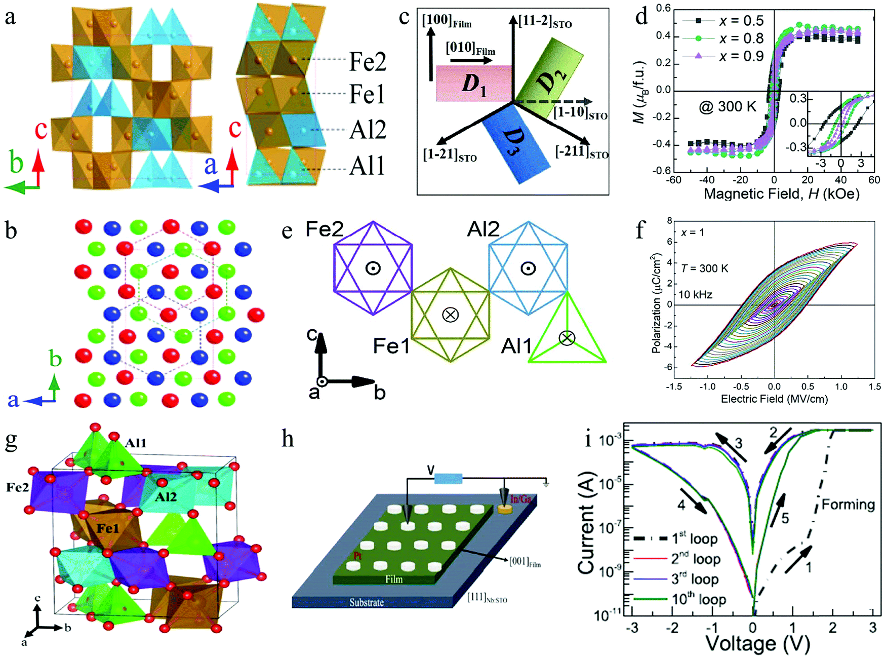 | ||
| Fig. 15 (a) Crystal structure of AlFeO3; (b) close-packed oxygen layers projected along the c-axis. Panels a and b reproduced with permission.154 Copyright 2014, AIP Publishing. (c) Schematic of the orientation relationship between film domains and the substrate; (d) room temperature hysteresis loops (M–H) with different compositions; (e) schematic of the direction of magnetic moments of Fe3+ ions at each site; (f) P–E hysteresis loops of AlFeO3 (x = 1) at 10 kHz with increasing maximum electric fields. Panels c–f reproduced with permission.155 Copyright 2020, Royal Society of Chemistry. (g) Model of the orthorhombic crystal structure of the AlFeO3 film; (h) schematic of the Pt/AlFeO3/Nb:STO heterostructure; (i) I–V loops of the heterostructure show the RS behavior. Panels g–i reproduced with permission.156 Copyright 2020, American Chemical Society. | ||
Importantly, Badari Narayana Rao et al. reported the multilevel RS characteristics of the Pt/AlFeO3/Nb-doped SrTiO3 (111) heterostructure.156 In this research, they carried out a systematic study to characterize and understood the switching process in the as-prepared RS device. A schematic of the crystal structure of the perovskite AlFeO3 is shown in Fig. 15g. The structure schematic of the RS device is shown in Fig. 15h, in which the Pt electrode with a diameter of 100 μm was deposited on the AlFeO3 film. Fig. 15i shows a typical bipolar I–V plot obtained from the Pt/AlFeO3/Nb-doped SrTiO3 heterostructure device, which clearly shows the presence of two resistance states (HRS and LRS) and the reversible transition between HRS and LRS. Finally, the mechanism of the Fe-redox process through the participation of oxygen vacancies and oxygen ions was proposed. Therefore, the multilevel RS can be realized in the Pt/AlFeO3/Nb-doped SrTiO3 heterostructure device. Indeed, the multilevel RS characteristics are attractive for high-density nonvolatile memories and neuromorphic computing.157–160 These results should inspire further research in order to achieve attractive RS properties with potential applicability in intelligent systems.
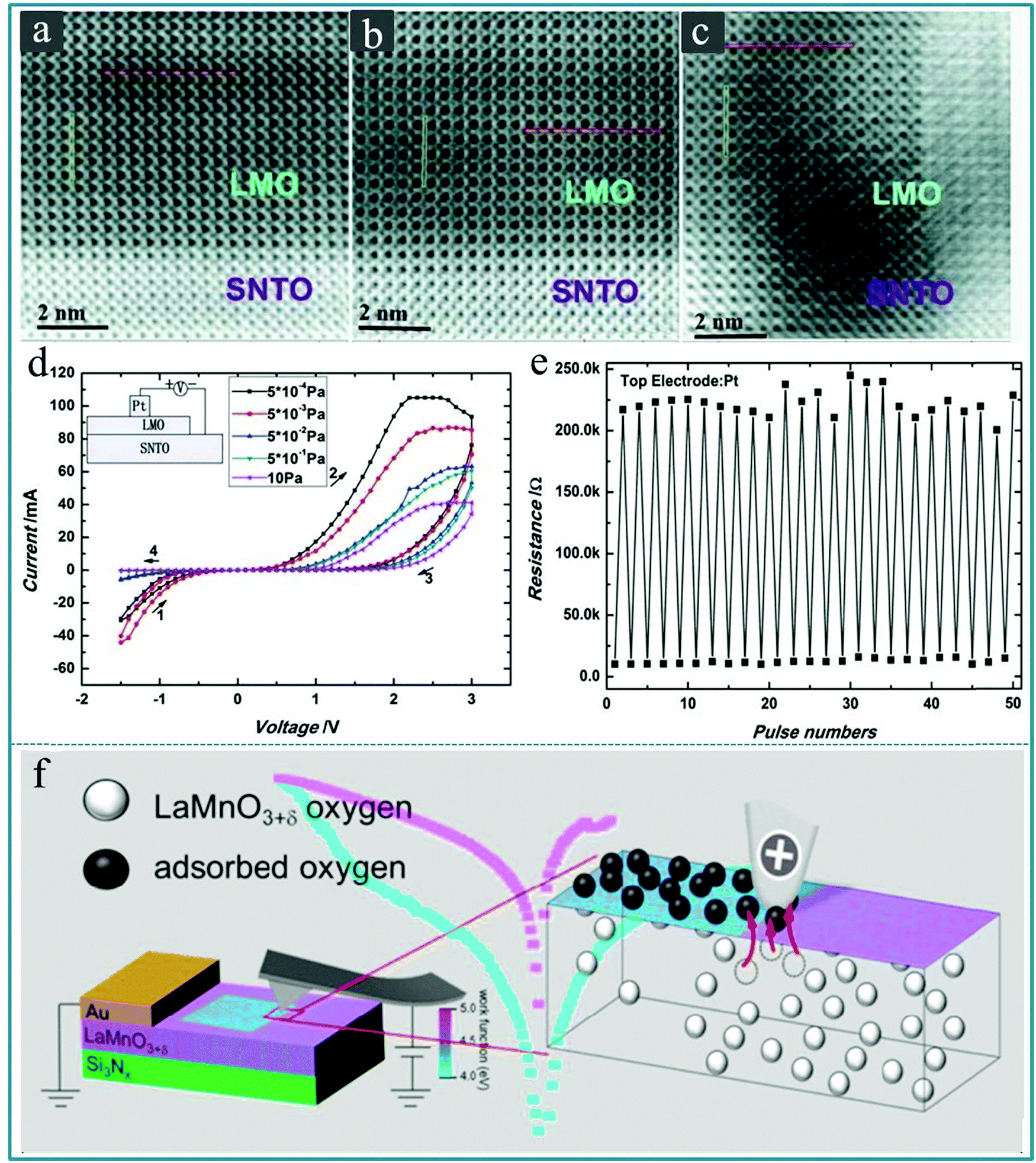
It is known that perovskite oxides are prone to generate oxygen vacancies due to the lack of oxygen during the preparation process,161 so it is generally considered that the oxygen vacancies are a major cause of the RS effect in perovskite oxide thin films with rich oxygen vacancies.162–164 Zhong-tang Xu et al. prepared LaMnO3 (LMO) films with different concentrations of oxygen vacancies on a SrTiO3:Nb (0.8 wt%) (SNTO) substrate by adjusting the oxygen pressure during the deposition process using vacuum deposition technology.165Fig. 16a–c displays the cross-sectional annular-bright-field (ABF) micrographs, in which some obvious changes can be seen at the LMO/SNTO interface when the preparation condition was changed. Furthermore, a RS memory device with Pt/LMO/SNTO structure was built using the as-prepared heterostructure. Fig. 16d displays the typical I–V characteristics of the Pt/LMO/SNTO device under various oxygen pressures. The inset of Fig. 16d exhibits the schematic setup for I–V measurements, in which Pt works as the top electrode and SNTO works as the bottom electrode. We can see that the resistance window of the device in the positive voltage region gradually decreases as the oxygen pressure increases, which implies that the oxygen vacancy concentration can effectively affect the RS performance of the Pt/LMO/SNTO device. Finally, to evaluate the stability of the Pt/LMO/SNTO device for information storage applications, the endurance measurements were further performed for the as-fabricated Pt/LMO/SNTO device under a stable oxygen pressure of 5.0 × 10⁻⁴ Pa. The device did not show significant attenuation after 50 testing cycles, as shown in Fig. 16e. Therefore, it is a feasible method to control the concentration of oxygen vacancies in the perovskite oxide by controlling the oxygen pressure during the vacuum deposition process or the subsequent annealing treatment in the oxygen atmosphere of the sample, thereby controlling its RS memory performance. Furthermore, Benjamin Meunier et al. prepared a RS device using a perovskite LaMnO3+δ thin film with a thickness of 25 nm as a functional layer on the SiNx/SiO2/Si substrate by chemical vapor deposition (CVD).166 It was found, based on conductive atomic force microscopy (c-AFM), that the resistance change would be triggered when the oxygen ions were adsorbed on the surface, as shown in Fig. 16f. This work provides a complete and comprehensive description of the physical mechanism involved in the interface resistance conversion on the surface of the LaMnO3+δ film based on the oxygen content.
 | ||
| Fig. 16 (a–c) Annular-bright-field (ABF) micrographs of the LMO/SNTO interfaces along the [001] axis corresponding to oxygen pressures of 10, 5 × 10⁻², and 5 × 10⁻⁴ Pa, respectively, in which La is represented by the darkest spots, whereas O is represented by the lightest spots. (d) Typical I–V curves for Pt/LMO/SNTO devices under oxygen pressures of 10, 5 × 10⁻¹, 5 × 10⁻², 5 × 10⁻³, and 5 × 10⁻⁴ Pa. The direction of bias sweeping is indicated by arrows, and the inset shows the measurement configuration of the devices. (e) Pulse measurements of the Pt/LMO/SNTO devices with a fabrication oxygen pressure of 5 × 10⁻⁴ Pa; the pulse condition for the HRS is +5.0 V with a pulse width of 1 ms and for the LRS it is −5.0 V with a pulse width of 1 ms, and the resistance was read out at 0.1 μA. Panels a–e reproduced with permission.165 Copyright 2012, Wiley-VCH. (f) Schematic diagram of the microscopic mechanisms of local interfacial RS in LaMnO3+δ. Reproduced with permission.166 Copyright 2020, American Chemical Society. | ||
It should be mentioned that single crystal LaAlO3 has the characteristics of good lattice matching to a variety of perovskite structure materials, and is usually used as a substrate material for preparing perovskite thin films.167 The dielectric properties of LaAlO3 are favorable for low-loss microwave and dielectric resonance applications.168 Generally, LaAlO3 has stable chemical properties and is insoluble in mineral acids at room temperature.169 LaAlO3 usually has a hexagonal crystal structure at room temperature, and it will transform into a cubic structure when the temperature exceeds 400 °C.170,171 Tom Wu’ group reported the RS memory behavior of the Pt/LaAlO3/SrTiO3 (Pt/LAO/STO) device.172 The structures of the memristor and FET are shown in Fig. 17a. It can be seen that the uppermost unit cell of LAO is discontinuous, which implies that there is a certain degree of transitional fluctuation in the thickness of the LAO layer (Fig. 17b). The interface between the LAO layer and the STO substrate is atomically flat, which is indicated by arrows in Fig. 17c. The I–V curves of the Pt/LAO/STO device exhibit a significant RS feature in an applied voltage sweep from −4.0 to 4.0 V, as shown in Fig. 17d. At the same time, Fig. 17e shows good endurance and consistent performance during more than 2000 operation cycles. Finally, it was proposed that the RS behavior may be caused by the drift of the charged oxygen vacancies across the LAO/STO interface led by the electric field and the gap states led by defects in the ultrathin LAO layer. Besides, Zhaomeng Gao et al. developed a ferroelectric memristor, in which the 2D electron gas resistance can be changed at the LaAlO3/SrTiO3 heterointerface.173 The schematic of the Pt/BFO/LAO/STO heterostructure device is shown in Fig. 17f. Fig. 17g shows an optical image of the Pt/BFO/LAO/STO device and the measurement pattern. This work confirmed that the ABO3 perovskites heterojunction device exhibited intriguing properties, which can be respected to be used as nonvolatile memories and photodetectors in electronics. Therefore, it can be concluded that these metal–oxide–oxide heterojunctions with atomically smooth interfaces and controlled defect transmission have good RS memory behavior, which provides a development space for integrated logic and nanoelectronics for memory technology. Here, we should note that the LaAlO3/SrTiO3 heterojunction has many important applications, such as superconductivity, two-dimensional (2D) electron gas, spin-valve devices, etc.174–178 These important applications stem from special interface effects of LaAlO3/SrTiO3. Therefore, the interface effect of the perovskite heterojunction is a very important research topic in material applications.
 | ||
| Fig. 17 (a) Proposed scheme of integrating both the high performance memristor and FET at the oxide interfaces; (b) high-resolution high-angle annular dark-field scanning transmission-electron-microscopy (HAADF-STEM) images of a Pt/LAO/STO heterostructure; (c) high-resolution image of the LAO/STO interface, which is marked by arrows; (d) forming process (voltage sweeps 1–4) transforms the device into the switchable states (sweeps 5–8); the red and the blue lines represent the LRS and HRS, respectively, and the arrows mark the directions of the sweeping voltage; (e) the endurance data with a readout voltage of 0.2 V. Panels a–e reproduced with permission.172 Copyright 2013, American Physical Society. (f) Schematic of the Pt/BFO/LAO/STO heterostructure; (g) the optical image of the Pt/BFO/LAO/STO structure and measurement. Panels f–g reproduced with permission.173 Copyright 2018, Wiley-VCH. | ||
Finally, we should mention a special perovskite material PbTixZr1−xO3 (PZT), which is also the main component of piezoelectric ceramics. The piezoelectric properties of PZT not only change with the atomic ratio of Zr/Ti, but also change with different additives.179–182 When the additive has the same valence as Pb2+ and Zr4+ (Ti4+) and the ionic radius is similar, it can form a replacement solid solution. When the additive is different from Pb2+ and Zr4+, it can form A1+B5+O3 or A2+B3+O3 type compounds. In addition, PZT ceramics are usually sintered by Pb3O4, TiO2, ZrO2 and a small amount of additives at high temperature.183–185 Furthermore, PZT has a very wide range of applications. It can be used in ultrasonic transducers, underwater acoustic transducers, ceramic transformers, electroacoustic devices and pyroelectric detectors.186,187 In particular, as a transparent ferroelectric material, PZT can also be used in photoelectric switches, image recognition, image display, photosensitive imaging, etc.188 It also has obvious application advantages in RS devices.
Daniel Pantel et al. confirmed that the ferroelectric polarization direction and resistance state are closely related in the ferroelectric Pb(Zr0.2Ti0.8)O3 (PZT) based RS devices prepared by the self-assembly method.189 The preparation process of the metal-ferroelectric-metal (MFM) structure is sketched in Fig. 18a. Fig. 18b shows the perfect self-assembly of the spheres on the PZT surface into a single layer after metal deposition. At the same time, ordered metal nanostructures can be obtained by dissolving latex nanospheres in dichloromethane (Fig. 18c). In the test of the as-prepared ferroelectric nonvolatile memory device, a high resistance ratio of 1500 was obtained. In addition, Christoph Baeumer et al. proved that the degree of graphene doping and ferroelectric polarization have a two-way interdependence in the graphene/PbZr0.2Ti0.8O3 hybrid structure-based RS device,190 as shown in Fig. 18d. In particular, the memory device prepared by using graphene/PbZr0.2Ti0.8O3 as the functional layer has good non-volatility, so it can be used for non-volatile memory. This indicates that the doping of graphene can promote the reversible ferroelectric polarization of the PZT film, and the ferroelectric polarization of the PZT film can in turn control the type and density of carriers in the graphene.190 Therefore, it can be concluded from the above research works that perovskite-type PZT materials can be used in the preparation of RS devices for information memory applications. PZT is further expected to be prepared into a new type of multifunctional electronic device because it has multiple characteristics of piezoelectricity, ferroelectricity, transparency, etc.
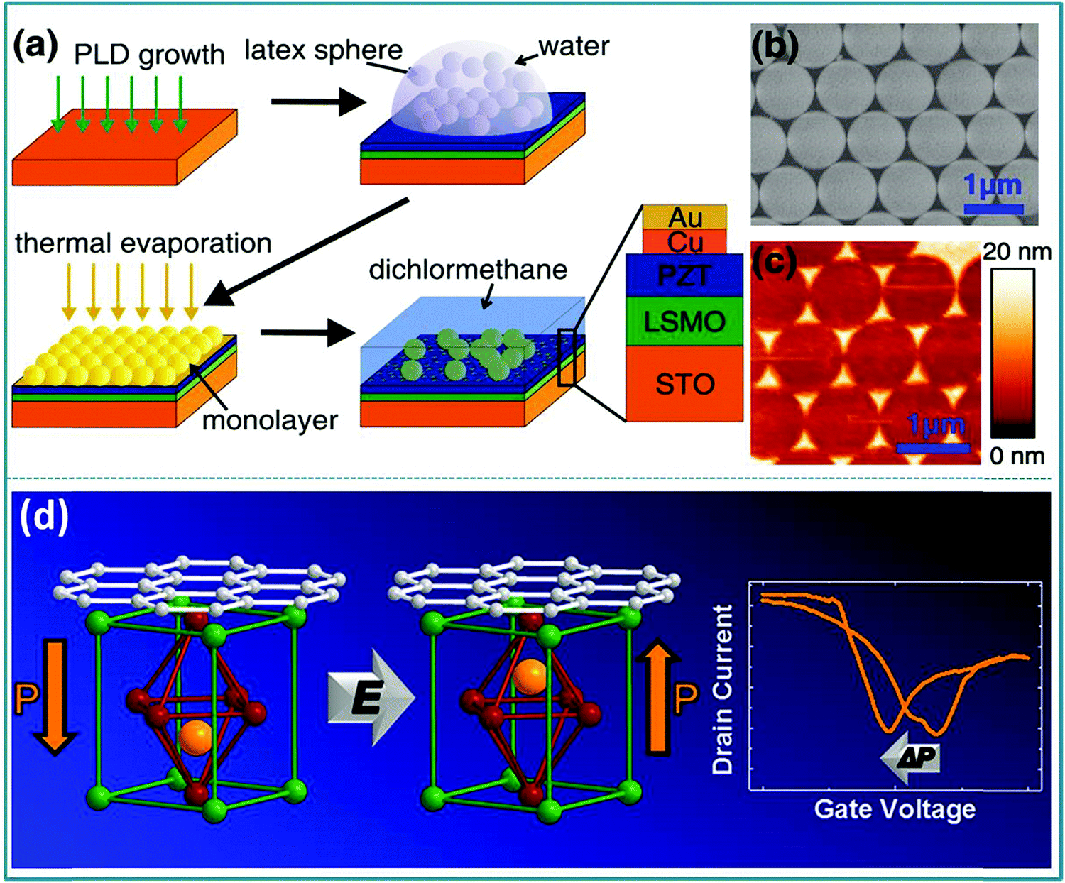 | ||
| Fig. 18 (a) Schematic of the nanosphere lithography (NSL) process adapted for nanoscale electrode preparation on PZT surfaces; (b) SEM image of a hexagonally close packed monolayer of polystyrene spheres; (c) the resulting Au-capped Cu nanoislands (by AFM) on top of a PZT surface. Panels a–c reproduced with permission.189 Copyright 2011, American Chemical Society. (d) Tunable carrier type and density in graphene/PbZr0.2Ti0.8O3 hybrid structures through ferroelectric switching. Reproduced with permission.190 Copyright 2013, American Chemical Society. | ||
3.2 The involved main mechanisms
It is well known that for any new physical phenomenon to be put into practical application a clear understanding of its mechanism is essential. The mechanism of the RS effect is often related to the formation of conductive filaments, the generation of Schottky barriers, the redox reaction of metal ions, ferroelectric polarization, etc.71–75 However, the mechanisms of RS effects are often different due to the diverse material selection. Firstly, to understand the mechanism of the RS effect based on ABO3-type multiferroic perovskite materials, Sahwan Hong et al. proposed the switchable Schottky-to-Ohmic interfacial contacts between electrodes and BiFeO3 nano-islands in a RS device with Pt/BiFeO3/SrRuO3 structure.71 The diagram of the physical mechanism is shown in Fig. 19a. It mainly explains the reversible change of the resistance states between HRS and LRS through the reversible transition of the interface barrier caused by the ferroelectric polarization reversal of the BiFeO3 layer under an external bias, and the mechanism agrees very well with the experimental data. Similar to the above report, Wanqiong Dai et al. explained the observed RS behavior in the La0.1Bi0.9FeO3/Nb-doped SrTiO3 (LBFO/NSTO) heterostructure by using the influence of ferroelectric polarization on the width of the depletion region and the modulation effect of the Schottky barrier height of the LBFO/NSTO interface,191 as shown in Fig. 19b. When a positive voltage pulse is applied to the Pt top electrode of the RS device, the polarization direction of the functional layer film is downward, and the generated positive electrode charge will be accumulated near the interface of the ferroelectric layer, thereby reducing the width of the depletion layer. When a negative voltage pulse is applied to the Pt top electrode of the RS device, a large number of carriers in the n-type semiconductor NSTO will be repelled by the negatively polarized accumulated charge, so that it can significantly increase the width of the depletion layer. Therefore, this work proves that it is possible to control the RS effect by adjusting the depletion width of the ferroelectric layer interface through ferroelectric polarization. Further, Lei Jin et al. attributed the variation in trap characteristics to changes in polarization ordering and trap densities, which were caused by the release of polarization domains and the generation of oxygen vacancies during the operation of the Au/BiFeO3/SrRuO3 device.192 As shown in Fig. 19c, most of the traps are empty at the beginning, leading to the device exhibit a low conductivity, which corresponds to HRS of the device. When a negative bias is applied on the top electrode of the device, the electrons can be captured by trap centers according to semiconductor theory. Thus, the Schottky barrier at the Au/BiFeO3 interface is lowered, and hence, this device exhibits a highly conductive behavior and the resistance state is switched from HRS to LRS. Subsequently, the trapped carriers still remain after the applied bias is removed, so the LRS can be retained until a positive bias is applied to switch the Au/BiFeO3/SrRuO3 device from LRS to HRS. In this way, this device can continuously complete the information processing between two resistance states (HRS and LRS) under an applied bias.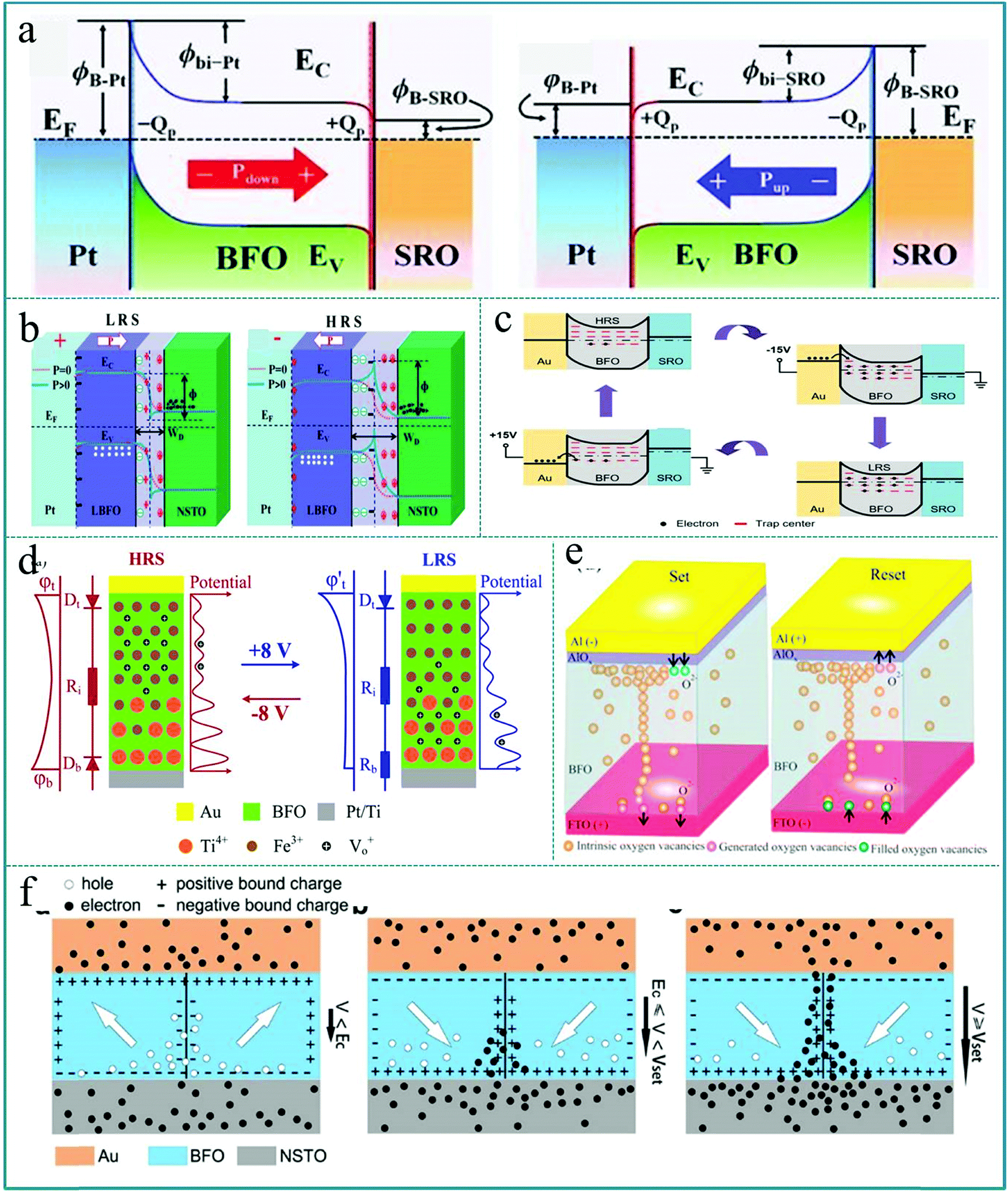 | ||
| Fig. 19 (a) Schematics of energy band diagrams of the Schottky-to-Ohmic interfacial contacts in Pt/BiFeO3/SrRuO3 modulated by polarization orientations. Reproduced with permission.71 Copyright 2013, Wiley-VCH. (b) Schematic of energy band diagrams of the Pt/La0.1Bi0.9FeO3/Nb-doped SrTiO3 heterostructure at LRS and HRS. Reproduced with permission.191 Copyright 2020, Royal Society of Chemistry. (c) Filling status of traps and the band diagram at the initial state of the device, negative voltage −15.0 V (applied), −15.0 V (removed), and +15.0 V (applied). Reproduced with permission.192 Copyright 2020 Elsevier. (d) Schematic representation of the distribution of mobile Vo+ (black circles) and fixed Ti4+ (orange circles) donors in the BiFeO3 thin film for HRS and LRS. Reproduced with permission.193 Copyright 2014, American Chemical Society. (e) Schematic of the AlOx assisted filament formation mechanism for set and reset states in Al/BiFeO3/FTO RRAM devices. Reproduced with permission.194 Copyright 2020, AIP Publishing. (f) Schematics showing the charged domain wall mediated RS mechanism of Au/BiFeO3/Nb-doped SrTiO3 heterojunctions. Reproduced with permission.195 Copyright 2020, Elsevier. | ||
Moreover, Tiangui You et al. established a modifiable Schottky barrier height model in a BiFeO3 memristor with abundant movable oxygen vacancies, and further clarified the physical mechanism of RS memory.193 As shown in Fig. 19d, the mechanism of the RS effect can be explained by adjusting the Schottky barrier of the BiFeO3/Pt interface, which means that the height of the Schottky barrier of the interface can be adjusted by applying an electric field to adjust the drift of the oxygen vacancies (Vo2+). Under the adjusted bias pulses, Vo2+ can act as a mobile donor and Ti4+ can act as a fixed donor in the BiFeO3 functional layer. Therefore, the RS behavior can be continuously configured by adjusting the amplitude and length of the applied bias pulse, which makes it possible to achieve multilevel memory logic and improve the switching speed. Chandni Kumari et al. used a low-cost process to fabricate a resistive random access memory (RRAM) device based on BiFeO3, and further studied the influence of the Al top electrode on the RS characteristic and reliability.194 The switching mechanism was clarified by the formation and fracture of oxygen vacancy conductive filaments and the participation of the AlOx thin layer on the Al/BiFeO3 interface, as shown in Fig. 19e. It should be known that the conductive filament mechanism is a very recognized mechanism of the RS effect. It is rarely limited to the type of functional material, and has a very close relationship with the type of electrode material. Finally, we should mention that M. J. Han fabricated a RS device based on high-density self-assembled BiFeO3 nano-islands grown on a Nb doped SrTiO3 (0.7 wt%) (NSTO) substrate.195 The RS property was induced by the formation and rupture of the conductive filament at the charged domain wall due to the change of charge carrier concentrations under the applied voltage. Fig. 19f shows a schematic diagram of the charge distribution in a charged domain wall under different applied voltages. In this device, the NSTO substrate is an n-type semiconductor, which makes the electrons here as carriers. In this way, a large number of electron carriers from the NSTO substrate will be effectively accumulated on the head-to-head charged domain wall. Therefore, this research provides us with a new way to improve the RS performance by adjusting the charged domain wall. In fact, because ferroelectric materials contain a large number of spontaneously polarized ferroelectric domains, the effect of the domain wall on nano-devices will stimulate new ideas in the construction of nanoscale electronic devices in future.
Anyway, the physical mechanism of the RS effect is currently inconclusive. In other words, there is no mechanism that can fully and profoundly explain all the observed RS behaviors.196–198 Certainly, the RS mechanism of ABO3 type multiferroic perovskite materials is still under extensive exploration. In the above discussion, we have only listed a few typical mechanisms. Therefore, in future research, the physical mechanism of the RS device is still a focus that needs to be further studied.199,200
4. ABO3 memristor-based synaptic device for neuromorphic computing
A synaptic device is an electrical device that can simulate the function of neurons for information transmission. According to the device structure, synaptic devices can be divided into synaptic transistors and synaptic memristors. Recently, the research of synaptic devices based on the memristive effect has received extensive attention. Neurons are the basic building blocks of the human brain, and synapse is the key part of transmitting information between neurons. Therefore, if we can develop electronic components with similar functions to biological synapses, it will be of great significance to realize artificial intelligence. Among all the known circuit elements, the memristor is a non-linear resistance device with information memory function, which has similar characteristics to the biological nerve synapse with nanometer size. Therefore, the memristive unit is one of the ideal electronic devices to realize synaptic function.201,202 In the study of synaptic devices based on memristors, Sören Boyn et al. reported a synapse device based on ferroelectric tunnel heterojunctions and observed the spike-timing-dependent plasticity (STDP).203 Among them, synaptic strength can be characterized through STDP based on the time and dependence of the electrical signals of neighboring neurons. Fig. 20a shows a memristive device with Pt/Co/BiFeO3/(Ca,Ce)MnO3/YAlO3 (Pt/Co/BFO/CCMO/YAO) multilayer structure, and the resistance of the device strongly depends on the relative fraction of ferroelectric domains. In order to construct a neural network using the as-prepared sandwich memristive unit, the simulated neural network was built using a crossbar array of 9 × 5 ferroelectric memristors (Fig. 20b). In a typical crossbar structure, each cross section represents a device unit. Using this method, neural networks can be constructed. Fig. 20c shows that the image recognition rate of the neural network increases with the increase of the number of image presentations, reaching almost 100% for low noise levels and nearly 80% for high noise levels. These experimental results lay the experimental foundation for the realization of low-power hardware for billions of reliable and predictable artificial synapses (such as deep neural networks) in artificial brain-based computers in the future,204,205 which can be effectively applied to the intelligent recognition of images and information.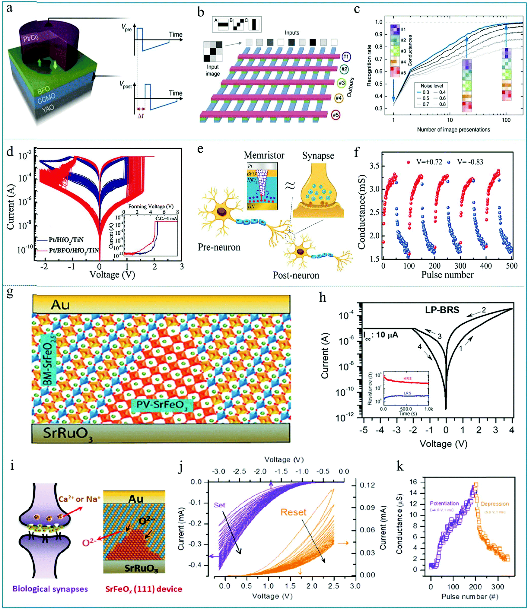 | ||
| Fig. 20 (a) Sketch of the ferroelectric memristor where a ferroelectric tunnel barrier of BiFeO3 (BFO) is sandwiched between the bottom electrode of (Ca,Ce)MnO3 (CCMO) and the top submicron pillar of Pt/Co, and YAO stands for YAlO3; (b) simulated spiking neural network comprising nine input neurons connected to five output neurons by an array of ferroelectric memristors, in which the inputs are noisy images of the patterns to be recognized: horizontal (A), diagonal (B) and vertical (C) bars in 3 × 3 pixel images; (c) recognition rate as a function of the number of presented images for different noise levels, in which the colored images are conductance maps of the memristors in each line and show their evolution for a noise level of 0.3 (blue line). Panels a–c reproduced with permission.203 Copyright 2016, Nature Publishing Group. (d) 100 continuous I–V curves for HfO2-based memristors with and without the BiFeO3 layer, and the inset shows the forming process. (e) Schematic diagram of the brain neural network and a Pt/BiFeO3/HfO2/TiN synaptic memristor; (f) the reproducible conductance modulation under repeated potentiation and depression pulses to mimic the change of synaptic weight in the biological synapse. Panels d–f reproduced with permission.206 Copyright 2020, Wiley-VCH. (g) Schematic representation of the Au/BM-SrFeO2.5 (111)/SrRuO3/SrTiO3 (111) device with the PV-SrFeO3 conductive path; (h) typical I–V curves of the device; (i) schematic representation of the bio-synapse and the conductive path formation. (j) I–V curves under consecutive negative voltage sweeps (blue lines) and positive voltage sweeps (orange lines, after the negative voltage sweeps). (k) Current in the synaptic device was gradually increased and decreased under the read voltage of 0.5 V. Panels g–k reproduced with permission.208 Copyright 2020, American Chemical Society. | ||
In recent research, Lei Liu et al. mimicked some biological synaptic functions based on a Pt/BiFeO3/HfO2/TiN memristor with an RS area of ∼1.0 × 1.0 μm2.206Fig. 20d shows a stable bipolar RS behavior of HfO2-based memristors with and without the BiFeO3 inserted layer. It is obvious that an enlarged resistance window can be achieved by adding the BiFeO3 inserted layer into the functional layer. Fig. 20e schematically illustrates the similar synapse structure and transmission characteristic of a memristor. Indeed, the biosynaptic weight reflects the connection strength of neurons, which can be represented by the conductance or resistance of the memristor.207 As shown in Fig. 20f, the conductance of the memristive device can be adjusted periodically by applying a voltage pulse, which is similar to the information transmission characteristic of a synapse. It is feasible to simulate the function of bio-synapse by adjusting the conductance of the memristor. This device can be applied to wearable systems and biomedical equipment. Therefore, this work proves that Pt/BiFeO3/HfO2/TiN memristors have potential applications in neuromorphic computing and artificial intelligence systems, opening up a new way for the integration of neural networks. Finally, it should be noted that Venkata Raveendra Nallagatla et al. studied the RS effect of the epitaxial brownmillerite SrFeO2.5 (BM-SrFeO2.5) thin film by systematically controlling the oxygen concentration to realize synaptic learning.208 This synaptic device exhibited either bipolar RS or complementary RS behaviors. Fig. 20g shows the synaptic device with Au/BM-SrFeO2.5 (111)/SrRuO3/SrTiO3 (111) structure which has out-of-plane-oriented oxygen-vacancy channels with the BM-SrFeO2.5 insulating layer. The typical I–V curves are shown in Fig. 20h, indicating a low-power bipolar RS property under a current compliance (CC) of 10 μA in the negative voltage region; the arrows in the figure indicate the direction of the applied voltage sweeps. The retention testing is shown in the inset of Fig. 20h, which presents a large switching window accompanied by a weak attenuation. This result implies that the RS device can be used in information processing and memory technology. Fig. 20i displays a schematic diagram of a bio-synapse, and the SrFeOx(111) RS device can be used to simulate the synaptic function. Fig. 20j shows the I–V curves under consecutive negative voltage sweeps (blue lines) and positive voltage sweeps (orange lines, after the negative voltage sweeps). Fig. 20k shows that the current of the RS device can be gradually increased by a consecutive potentiating electric pulse of −4.0 V ms−1 and decreased by a depressing electric pulse of 5.0 V ms−1 under a read voltage of 0.5 V, indicating that the RS device can be useful for synaptic operations in smart applications.
Therefore, it can be confirmed that the memristor unit is an effective component to realize artificial intelligence hardware.209 In the brain, the basic law of biological memory and learning is synaptic plasticity. Artificial synaptic devices are required to achieve synaptic weight adjustment with good stability and repeatability under appropriate excitability and pulse stimulation. The condition for simulating the plasticity of biological nerve synapses is that the conductance (or resistance) of the artificial synaptic device can be continuously adjusted. The resistance of the memristor can be changed with the amount of charge flowing through it, and the resistance can be maintained after power failure state, so the memristor is considered to be an ideal device to simulate nerve synapses.210,211 The synaptic devices reported so far are based on the principle of oxygen vacancy migration to realize the time-dependent synaptic plasticity (STDP) function of neuronal electrical pulse activity.212,213 Therefore, the effect of this sequence of synaptic activity on synaptic information transmission is considered to be directly related to brain learning and memory functions.
Actually, neuromorphic computing is a process that mimics the information processing at biological synapses. The neuromorphic computing can realize high-efficiency massive parallel computing to conquer the limitation of the Von Neumann bottleneck.214–219 The physical mechanism of neuromorphic computing is based on the ion transport at the device interface to achieve efficient transfer and computation of information at the same location,220 which is different from the logic circuit in digital systems.221 Besides, neuromorphic computing is characterized by distributed memory and computational elements.222 For the research and application of memristive devices, neuromorphic computing is a necessary step for memristors to be applied to artificial intelligence.223 Many recent studies have effectively proved that the use of memristors in neuromorphic computing has practical significance and research foundation.224
In previous reports, it has been proved that the BiFeO3 single-crystal orientation films can be successfully prepared using appropriate technical means.225–227 Haoyang Sun grew high-quality (111)-oriented BiFeO3 ferroelectric films on flexible mica substrates with SrRuO3/BaTiO3 double buffer layers, and a ferroelectric memristive behavior with continuously tunable resistance states was observed.228 The BaTiO3, SrRuO3, and BiFeO3 films have a quasi-hexagonal structure. As shown in Fig. 21a, with the pulse duration td = 10 μs, the memristor is set to the LRS by an applied voltage of +13.0 V or the HRS by an applied voltage of −16.0 V. Then, using the as-prepared memristor device, a two-layer perceptron with 784 input neurons, 100 hidden neurons, and 10 output neurons was simulated, as shown in Fig. 21b. Fig. 21c shows the deep neural network (DNN) with a flexible BiFeO3 memristor, which can reach a pattern recognition accuracy of ∼90% after 1500 training cycles. Therefore, this study shows that it is feasible to prepare high-quality multiferroic perovskite films on flexible substrates. It also confirms that the flexible ferroelectric memristive devices have obvious advantages in non-volatile information processing and neuromorphic computing in advanced artificial intelligence systems.229 Haoyang Sun et al. used an ultra-thin BiFeO3 ferroelectric barrier layer, a ZnO semiconductor layer and a SrRuO3 electrode to prepare a flexible ferroelectric tunnel junction (FTJ) memristor, and found that the FTJ memristor shows multistable memory behavior.230 In this study, a perceptron neural network (784 × 100 × 10) was constructed to recognize Modified National Institute of Standard and Technology (MNIST) handwritten digits, as shown in Fig. 21d. After 3000 training cycles, a high recognition accuracy of 92.8% can be achieved using this neural network (Fig. 21e). In addition to the two-layer artificial neural network that can be used to recognize handwritten digits, they further built a more complex three-layer perceptron neural network (784 × 1024 × 512 × 10) to recognize the Fashion-MNIST (F-MNIST) image dataset as shown in Fig. 21f. After 55![[thin space (1/6-em)]](https://www.rsc.org/images/entities/char_2009.gif) 000 cycles, the neural network can still achieve an image recognition accuracy of 86.2%, as shown in Fig. 21g. This research may provide a new path for the development of nonvolatile memory and neuromorphic computing systems based on flexible FTJ memristors.
000 cycles, the neural network can still achieve an image recognition accuracy of 86.2%, as shown in Fig. 21g. This research may provide a new path for the development of nonvolatile memory and neuromorphic computing systems based on flexible FTJ memristors.
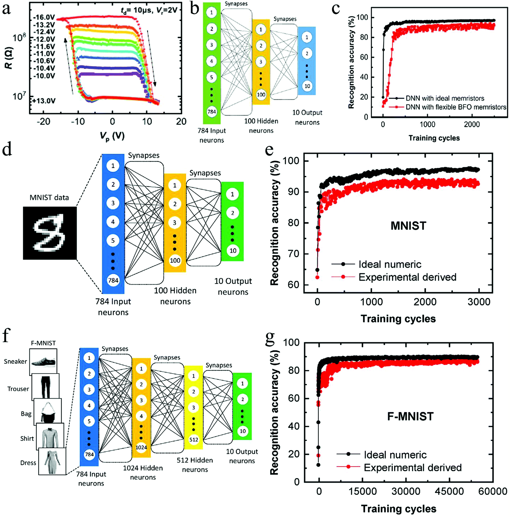 | ||
| Fig. 21 (a) Resistances as a function of Vp with td = 10 μs, in which the arrows indicate the sweeping directions of Vp; (b) schematic diagram of a two-layer perceptron neural network; (c) simulation results based on the realistic device behavioral model and ideal synaptic devices. Panels a–c reproduced with permission.228 Copyright 2020, American Chemical Society. (d) Schematic diagram of a two-layer perceptron neural network (784 × 100 × 10) trained to clarify the 28 × 28 MNIST pixel handwritten digits, and (e) the corresponding recognition accuracies for experimental and ideal synaptic devices; (f) schematic diagram of a three-layer neural network (784 × 1024 × 512 × 10) trained to clarify the 28 × 28 FMNIST pixel images, and (g) the corresponding recognition accuracies based on experimental and ideal synaptic devices. Panels d–g reproduced with permission.230 Copyright 2021, Elsevier. | ||
Furthermore, Yihao Yang et al. demonstrated a memristive ferroelectric tunnel junction (FTJ) synapse based on the multiferroic BaTiO3/CoFe2O4 composite.231Fig. 22a shows the schematic of the (La0.67, Sr0.33)MnO3 (LSMO)/BaTiO3 (BTO)/CoFe2O4 (CFO)/Nb:SrTiO3 (Nb:STO) FTJ device. Fig. 22b shows the schematic of the piezoresponse force microscopy (PFM) measurements, in which the arrows inside the BTO layer represent polarizations. Fig. 22c shows that one can implement the neuromorphic computing by constructing a cross-node neural network based on the spin filter LSMO/BTO/CFO/Nb:STO memristive FTJ as an artificial synaptic unit, thereby realizing the long-term plasticity of each node of the brain-inspired intelligent recognition. Therefore, the memristive FTJ device provides a new approach toward neuromorphic computing with energy-efficiency, which further expands the broad scope of applications. Moreover, Rao et al. used epitaxy to prepare a high crystallinity SrFeOx heterojunction and characterized the memristive properties of the Au/SrFeOx/SrRuO3 device.232Fig. 22d shows the schematic of a conductive filament induced RS device consisting of a brownmillerite SrFeO2.5 (BM-SFO) matrix and a perovskite SrFeO3 (PV-SFO) conductive filament, and Fig. 22e shows an interface effect induced RS device consisting of a PV-SFO matrix and a BM-SFO interfacial layer. The hysteresis-type I–V characteristics are shown in Fig. 22f and g, in which it can be found that the RS effect induced by the conductive filament has a more obvious SET and RESET process, and it is usually accompanied by a larger HRS/LRS resistance ratio. In this work, they found that the SrFeOx based memristive device exhibits an excellent synaptic function, which can be used to construct neuromorphic computing circuits.232Fig. 22h and i presents a simulation diagram of a three-layer neural network with a crossbar consisting of SrFeOx-based synaptic memristors, which can effectively recognize images with accuracies of ∼88%, indicating that SrFeOx-based synaptic memristors as building blocks have important potential applications in neuromorphic computing circuits.
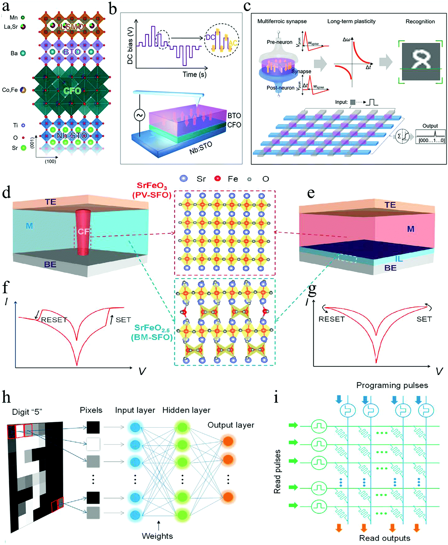 | ||
| Fig. 22 (a) Schematic of the LSMO/BTO/CFO/Nb:STO FTJ; (b) schematic of the PFM measurements, in which the arrows inside the BTO layer represent polarizations; (c) schematic of the neuron simulation from long-term plasticity of the LSMO/BTO/CFO/Nb:STO multiferroic synapses to the recognition functionality in a crossbar network. Panels a–c reproduced with permission.231 Copyright 2020, American Chemical Society. (d–g) Schematic of the different RS device structures and I–V characteristics; (h) schematic of a three layer neural network; (i) a crossbar consisting of SrFeOx-based synapses. Panels d–i reproduced with permission.232 Copyright 2021, Elsevier. | ||
5. Summary and outlook
Table 1 exhibits the comparison results of the typical ABO3-based memristive devices in terms of the switching function layer, electrode schedule, cycling endurance, retention time, HRS/LRS ratio, and energy consumption. Among these features, the cycling endurance exceeds 107 for the SrFeOx-based memristive device with ∼pJ energy consumption. Importantly, the oxygen-rich stoichiometry of ABO3 endows the memristor with a variety of RS behaviors to faithfully mimic the neuron networks. Electrode engineering as one of the most efficient methods to obtain the target RS behavior such as the binary, electron-type, and analog RS behavior was extensively investigated for application in T bits data storage and neuromorphic computing.233 Although great progress has been made in ABO3-based memristors in recent years, the sneak current issue has not been overcome because of the lack of an ideal ABO3 memristive cell. One possible solution is optimizing the preparation methods to develop a self-rectification ABO3-based memristor or integrate the stable ABO3-based memristor with back-to-back diodes to enlarge the memristor crossbar array.| Functional layer | Top electrode | Bottom electrode | Endurance (cycles) | Retention (s) | HRS/LRS ratio | Energy consumption | Ref. |
|---|---|---|---|---|---|---|---|
| BiFeO3 | Pt | SrRuO3 | — | 103 | 753 | — | 71 |
| BiFeO3 | SrRuO3 | Nb-Doped SrTiO3 | 15 | — | 593 | — | 72 |
| BiFeO3 | Pt | SrRuO3 | 24 | 6 × 10³ | 103 | — | 77 |
| Co-Doped BaTiO3 | Au | Pt | 1 × 10⁵ | 7 × 10⁴ | >104 | — | 106 |
| BaTiO3 | Au | La0.75Sr0.25MnO3 | — | — | ∼18 | — | 107 |
| BaTiO3 | Conductive cantilever of AFM | La0.7Sr0.3MnO3 | — | — | — | — | 119 |
| Nb-Doped SrTiO3 | Pt | Nb-Doped SrTiO3 | 36 | — | — | — | 137 |
| LaAlO3 | ITO | SrTiO3 | 2 × 10³ | 4 × 10⁴ | ∼102 | — | 138 |
| SrTiO3 | Pt | Pt | — | — | — | — | 139 |
| Fe-Doped SrTiO3 | Ag | Pt | 2.5 × 10³ | — | ∼105 | — | 140 |
| SrCoOx | Au | Nb-Doped SrTiO3 | 100 | 1 × 10⁴ | >103 | — | 149 |
| AlFeO3 | Pt | Nb-Doped SrTiO3 | 1 × 10⁴ | 1 × 10⁴ | ∼102 | — | 156 |
| LaMnO3 | Pt | Nb-Doped SrTiO3 | 50 | — | ∼18 | — | 165 |
| LaMnO3+δ | Conductive cantilever of AFM | Au | — | — | — | — | 166 |
| LaAlO3 | Pt | SrTiO3 | 2 × 10³ | 4.32 × 10⁴ | ∼102 | — | 172 |
| BiFeO3/LaAlO3 | Pt | SrTiO3 | — | — | ∼102 | — | 173 |
| BiFeO3/HfO2 | Pt | TiN | 100 | 1 × 10⁴ | ∼104 | 206 | |
| SrFeO2.5 | Au | SrRuO3 | 1 × 10³ | — | >10 | 208 | |
| SrFeOx | Au | SrRuO3 | 1 × 10⁷ | — | >10 | ∼0.24 pJ per spike | 232 |
The ABO3-based memristor array has shown high capability in operating the convolutional neural network (CNN), which has been extensively applied in image processing, language recognition, automatic driving, and so on.234–237 The ABO3-based memristor array has shown great potential application in neuromorphic computing,238–242 but the insufficient hashrate is also a bottleneck for complicated applications. One solution is constructing an analog-type ABO3-based memristor with high precision and developing ultrahigh scale integration technologies (i.e., nano imprint, directed self-assembly, DSA) to improve the capability of parallel computing.243–247Fig. 23 schematically demonstrates the ABO3-based materials including BiFeO3, BaTiO3, SrRuO3, LaMnO3, and AlFeO3 for the internal dynamic process to faithfully mimic our human brain. By constructing a large scale ABO3-based memristor array, the ABO3-based memristor array enables the high efficiency neuromorphic computing.
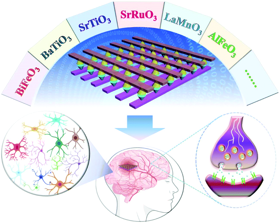 | ||
| Fig. 23 The development from ABO3-type multiferroic perovskite materials to artificial intelligence applications. | ||
In addition, multiferroic perovskite materials also have potential for application in spintronic devices.248–252 The interactive coupling of ferroelectric domains and magnetic domains makes electron spin more diversified. Besides, multiferroic heterojunctions with both ferroelectric and ferromagnetic properties can achieve voltage-regulated magnetic properties or magnetic field-regulated ferroelectric properties through magnetoelectric coupling effects, which provides the possibility to generate spin currents. Therefore, the research of multiferroic perovskite materials in neuromorphic technology is expected to produce new physical phenomena and advanced applications.
Finally, it should be noted that multiferroic perovskite materials can also be used in the field of catalysis.253–257 For example, multiferroic perovskite type Bi5CoTi3O15 exhibits high electrocatalytic efficiency due to the synergistic effect of electron spin and ferroelectric polarization.258 Thus, multiferroic perovskite materials have a wide range of potential applications in materials science, physics, chemistry, electronics, informatics, and computer science. And, the all-round research on this multifunctional perovskite material is expected to explore its powerful functions for better serving scientific and technological requirements in interdisciplinary fields.259,260
In summary, we have discussed in detail the research progress of ABO3 multiferroic perovskite materials in the preparation of memristive devices, the realization of synaptic devices, the construction of neural networks, and neuromorphic computing. Because the ABO3 multiferroic perovskite materials have unique electron spin, transfer, polarization, and coupling behaviors, they show a very potential application in multifunctional electronics when combining their advantages of multiferroic properties with the memristive effect. These devices have already laid a scientific foundation for the manufacture of spin-moment-based multistate memristive memory devices. This domain wall feature in multiferroic perovskite materials generally improves the mutual controllability of the memristive effect and the electron spin effect. Therefore, it is expected to play more important applications in computer science, electronics, biomedicine, etc.
Author contributions
B. Sun drafted this review and made detailed revisions. G. Zhou and L. Sun polished up English writing and grammar correction. H. Zhao, Y. Chen, F. Yang, and Y. Zhao made some discussions. Q. Song gave some useful suggestions and guidance. All authors gave their approval to the final version of the manuscript.Conflicts of interest
The authors declare no conflict of interest.Acknowledgements
The authors gratefully acknowledge financial support from the National Natural Science Foundation of China (Grant No. 11774293), the Sichuan Science and Technology Program (Grant No. 2020YJ0086), and the Fundamental Research Funds for the Central Universities (Grant No. 2682021CX076).References
- J. G. Simmons and R. R. Verderber, Proc. R. Soc. A, 1967, 301, 77–102 CAS.
- L. Chua, IEEE Trans. Circuit Theory, 1971, 18, 507–519 Search PubMed.
- D. B. Strukov, G. S. Snider, D. R. Stewart and R. S. Williams, Nature, 2008, 453, 80–83 CrossRef CAS PubMed.
- X. Chen, N. Wu, J. Strozier and A. Ignatiev, Appl. Phys. Lett., 2006, 89, 063507 CrossRef.
- J. Choi, S. Park, J. Lee, K. Hong, D.-H. Kim, C. W. Moon, G. D. Park, J. Suh, J. Hwang, S. Y. Kim, H. S. Jung, N.-G. Park, S. Han, K. T. Nam and H. W. Jang, Adv. Mater., 2016, 28, 6562–6567 CrossRef CAS PubMed.
- X. Zhu, J. Lee and W. D. Lu, Adv. Mater., 2017, 29, 1700527 CrossRef PubMed.
- Y. Wang, Z. Lv, Q. Liao, H. Shan, J. Chen, Y. Zhou, L. Zhou, X. Chen, V. A. L. Roy, Z. Wang, Z. Xu, Y.-J. Zeng and S.-T. Han, Adv. Mater., 2018, 30, 1800327 CrossRef PubMed.
- J. Choi, Q. V. Le, K. Hong, C. W. Moon, J. S. Han, K. C. Kwon, P.-R. Cha, Y. Kwon, S. Y. Kim and H. W. Jang, ACS Appl. Mater. Interfaces, 2017, 9, 30764–30771 CrossRef CAS PubMed.
- X. Guan, W. Hu, M. A. Haque, N. Wei, Z. Liu, A. Chen and T. Wu, Adv. Funct. Mater., 2018, 28, 1704665 CrossRef.
- L. Chua, Semicond. Sci. Technol., 2014, 29, 104001 CrossRef.
- G. Zhou, B. Sun, X. Hu, L. Sun, Z. Zou, B. Xiao, W. Qiu, B. Wu, J. Li, J. Han, L. Liao, C. Xu, G. Xiao, L. Xiao, J. Cheng, S. Zheng, L. Wang, Q. Song and S. Duan, Adv. Sci., 2021, 8, 2003765 CrossRef CAS.
- G. Zhou, Z. Ren, L. Wang, B. Sun, S. Duan and Q. Song, Mater. Horiz., 2019, 6, 1877–1882 RSC.
- B. Sun, Y. Chen, M. Xiao, G. Zhou, S. Ranjan, W. Hou, X. Zhu, Y. Zhao, S. A. T. Redfern and Y. N. Zhou, Nano Lett., 2019, 19, 6461–6465 CrossRef CAS PubMed.
- B. Sun, G. Zhou, T. Guo, Y. N. Zhou and Y. A. Wu, Nano Energy, 2020, 75, 104938 CrossRef CAS.
- S. Ranjan, B. Sun, G. Zhou, Y. A. Wu, L. Wei and Y. N. Zhou, ACS Appl. Nano Mater., 2020, 3, 5045–5052 CrossRef CAS.
- M. Hu, C. E. Graves, C. Li, Y. Li, N. Ge, E. Montgomery, N. Davila, H. Jiang, R. S. Williams, J. J. Yang, Q. Xia and J. P. Strachan, Adv. Mater., 2018, 30, 1705914 CrossRef PubMed.
- P. M. Sheridan, F. Cai, C. Du, W. Ma, Z. Zhang and W. D. Lu, Nat. Nanotechnol., 2017, 12, 784–789 CrossRef CAS PubMed.
- X. Yan, J. Zhao, S. Liu, Z. Zhou, Q. Liu, J. Chen and X. Y. Liu, Adv. Funct. Mater., 2018, 28, 1705320 CrossRef.
- Z. Wang, S. Joshi, S. E. Savel’ev, H. Jiang, R. Midya, P. Lin, M. Hu, N. Ge, J. P. Strachan, Z. Li, Q. Wu, M. Barnell, G.-L. Li, H. L. Xin, R. S. Williams, Q. Xia and J. J. Yang, Nat. Mater., 2017, 16, 101–108 CrossRef CAS PubMed.
- Y. Wang, Z. Zhang, M. Xu, Y. Yang, M. Ma, H. Li, J. Pei and L. Shi, ACS Appl. Mater. Interfaces, 2019, 11, 24230–24240 CrossRef CAS PubMed.
- I. Boybat, M. L. Gallo, S. R. Nandakumar, T. Moraitis, T. Parnell, T. Tuma, B. Rajendran, Y. Leblebici, A. Sebastian and E. Eleftheriou, Nat. Commun., 2018, 9, 2514 CrossRef PubMed.
- B. Sun, S. Ranjan, G. Zhou, T. Guo, Y. Xia, L. Wei, Y. N. Zhou and Y. A. Wu, Mater. Today Adv., 2021, 9, 100125 CrossRef.
- M. A. Zidan, J. P. Strachan and W. D. Lu, Nat. Electron., 2018, 1, 22–29 CrossRef.
- Y. van de Burgt, A. Melianas, S. T. Keene, G. Malliaras and A. Salleo, Nat. Electron., 2018, 1, 386–397 CrossRef.
- Z. Wang, L. Wang, M. Nagai, L. Xie, M. Yi and W. Huang, Adv. Electron. Mater., 2017, 3, 1600510 CrossRef.
- P. Yao, H. Wu, B. Gao, J. Tang, Q. Zhang, W. Zhang, J. J. Yang and H. Qian, Nature, 2020, 577, 641–646 CrossRef CAS PubMed.
- S. Choi, J. H. Shin, J. Lee, P. Sheridan and W. D. Lu, Nano Lett., 2017, 17, 3113–3118 CrossRef CAS PubMed.
- Q. Xia and J. J. Yang, Nat. Mater., 2019, 18, 309–323 CrossRef CAS PubMed.
- Z.-H. Tan, R. Yang, K. Terabe, X.-B. Yin, X.-D. Zhang and X. Guo, Adv. Mater., 2016, 28, 377–384 CrossRef CAS.
- P. Cheng, K. Sun and Y. H. Hu, Nano Lett., 2016, 16, 572–576 CrossRef CAS PubMed.
- B. Sun, T. Guo, G. Zhou, J. Wu, Y. Chen, Y. N. Zhou and Y. A. Wu, ACS Appl. Bio Mater., 2021, 4, 1976–1985 CrossRef CAS.
- J. H. Yoon, Z. Wang, K. M. Kim, H. Wu, V. Ravichandran, Q. Xia, C. S. Hwang and J. J. Yang, Nat. Commun., 2018, 9, 1–9 CrossRef PubMed.
- Z. Lv, Y. Wang, J. Chen, J. Wang, Y. Zhou and S.-T. Han, Chem. Rev., 2020, 120, 3941 CrossRef CAS PubMed.
- W. Yi, K. K. Tsang, S. K. Lam, X. Bai, J. A. Crowell and E. A. Flores, Nat. Commun., 2018, 9, 1–10 CrossRef CAS.
- X. Hu, W. Wang, B. Sun, Y. Wang, J. Li and G. Zhou, J. Phys. Chem. Lett., 2021, 12, 5377–5383 CrossRef CAS.
- B. Sun, G. Zhou, K. Xu, Q. Yu and S. Duan, ACS Mater. Lett., 2020, 2, 1669–1690 CrossRef CAS.
- M. K. Hota, M. K. Bera, B. Kundu, S. C. Kundu and C. K. Maiti, Adv. Funct. Mater., 2012, 22, 4493–4499 CrossRef CAS.
- G. Kook, S. Jeong, M. K. Kim, S. Lee, N. Choi and H. J. Lee, Adv. Mater. Technol., 2020, 5, 1900991 CrossRef CAS.
- C. Zhang, W. B. Ye, K. Zhou, H.-Y. Chen, J.-Q. Yang, G. Ding, X. Chen, Y. Zhou, L. Zhou, F. Li and S.-T. Han, Adv. Funct. Mater., 2019, 29, 1808783 CrossRef.
- X. He, J. Zhang, W. Wang, W. Xuan, X. Wang, Q. Zhang, C. G. Smith and J. Luo, ACS Appl. Mater. Interfaces, 2016, 8, 10954–10960 CrossRef CAS PubMed.
- W. Eerenstein, N. D. Mathur and J. F. Scott, Nature, 2006, 442, 759–765 CrossRef CAS PubMed.
- X. Yang, Z. Zhou, T. Nan, Y. Gao, G. M. Yang, M. Liu and N. X. Sun, J. Mater. Chem. C, 2016, 4, 234–243 RSC.
- N. A. Spaldin and R. Ramesh, Nat. Mater., 2019, 18, 203 CrossRef CAS PubMed.
- T. Kosub, M. Kopte, R. Hühne, P. Appel, B. Shields, P. Maletinsky, R. Hübner, M. O. Liedke, J. Fassbender, O. G. Schmidt and D. Makarov, Nat. Commun., 2017, 8, 13985 CrossRef CAS PubMed.
- L. W. Martin and R. Ramesh, Acta Mater., 2012, 60, 2449–2470 CrossRef CAS.
- C. A. F. Vaz, J. Hoffman, C. H. Ahn and R. Ramesh, Adv. Mater., 2010, 22, 2900–2918 CrossRef CAS PubMed.
- M. Bibes and A. Barthélémy, Nat. Mater., 2008, 7, 425–426 CrossRef CAS PubMed.
- X. Lu, Y. Kim, S. Goetze, X. Li, S. Dong, P. Werner, M. Alexe and D. Hesse, Nano Lett., 2011, 11, 3202–3206 CrossRef CAS PubMed.
- J.-H. Lee, P. Murugavel, H. Ryu, D. Lee, J. Y. Jo, J. W. Kim, H. J. Kim, K. H. Kim, Y. Jo, M.-H. Jung, Y. H. Oh, Y.-W. Kim, J.-G. Yoon, J.-S. Chung and T. W. Noh, Adv. Mater., 2006, 18, 3125–3129 CrossRef CAS.
- T.-J. Park, G. C. Papaefthymiou, A. J. Viescas, A. R. Moodenbaugh and S. S. Wong, Nano Lett., 2007, 7, 766–772 CrossRef CAS PubMed.
- J. Ma, J. Hu, Z. Li and C.-W. Nan, Adv. Mater., 2011, 23, 1062–1087 CrossRef CAS PubMed.
- Y.-H. Chu, L. W. Martin, M. B. Holcomb and R. Ramesh, Mater. Today, 2007, 10, 16–23 CrossRef CAS.
- Y. Wang, D. Gray, D. Berry, J. Gao, M. Li, J. Li and D. Viehland, Adv. Mater., 2011, 23, 4111–4114 CrossRef CAS PubMed.
- C. Israel, N. D. Mathur and J. F. Scott, Nat. Mater., 2008, 7, 93–94 CrossRef CAS PubMed.
- P. Zhao, Z. Zhao, D. Hunter, R. Suchoski, C. Gao, S. Mathews, M. Wuttig and I. Takeuchi, Appl. Phys. Lett., 2009, 94, 243507 CrossRef.
- H. Greve, E. Woltermann, R. Jahns, S. Marauska, B. Wagner, R. Knöchel, M. Wuttig and E. Quandt, Appl. Phys. Lett., 2010, 97, 152503 CrossRef.
- L. Zhang, C. M. Leung, S. W. Or and S. L. Ho, J. Appl. Phys., 2013, 114, 027016 CrossRef.
- A. Hirohata and K. Takanashi, J. Phys. D: Appl. Phys., 2014, 47, 193001 CrossRef.
- H. Yan, Z. Feng, P. Qin, X. Zhou, H. Guo, X. Wang, H. Chen, X. Zhang, H. Wu, C. Jiang and Z. Liu, Adv. Mater., 2020, 32, 1905603 CrossRef CAS.
- L. Guo, X. Gu, X. Zhu and X. Sun, Adv. Mater., 2019, 31, 1805355 CrossRef CAS.
- P. Zheng, B. Sun, Y. Chen, H. Elshekh, T. Yu, S. Mao, S. Zhu, H. Wang, Y. Zhao and Z. Yu, Appl. Mater. Today, 2019, 14, 21–28 CrossRef.
- M. Overby, A. Chernyshov, L. P. Rokhinson, X. Liu and J. K. Furdyna, Appl. Phys. Lett., 2008, 92, 192501 CrossRef.
- D. Kan, L. Pálová, V. Anbusathaiah, C. J. Cheng, S. Fujino, V. Nagarajan, K. M. Rabe and I. Takeuchi, Adv. Funct. Mater., 2010, 20, 1108–1115 CrossRef CAS.
- D. Mazumdar, V. Shelke, M. Iliev, S. Jesse, A. Kumar, S. V. Kalinin, A. P. Baddorf and A. Gupta, Nano Lett., 2010, 10, 2555–2561 CrossRef CAS PubMed.
- J.-G. Park, M. D. Le, J. Jeong and S. Lee, J. Phys.: Condens. Matter, 2014, 26, 433202 CrossRef PubMed.
- A. Sarkar, A. K. Singh, D. Sarkar, G. G. Khan and K. Mandal, ACS Sustainable Chem. Eng., 2015, 3, 2254–2263 CrossRef CAS.
- R. Moubah, O. Rousseau, D. Colson, A. Artemenko, M. Maglione and M. Viret, Adv. Funct. Mater., 2012, 22, 4814–4818 CrossRef CAS.
- M. Shang, C. Zhang, T. Zhang, L. Yuan, L. Ge, H. Yuan and S. Feng, Appl. Phys. Lett., 2013, 102, 062903 CrossRef.
- R. Nechache, C. V. Cojocaru, C. Harnagea, C. Nauenheim, M. Nicklaus, A. Ruediger, F. Rosei and A. Pignolet, Adv. Funct. Mater., 2011, 23, 1724–1729 CrossRef CAS PubMed.
- C. M. Fernández-Posada, A. Castro, J.-M. Kiat, F. Porcher, O. Peña, M. Algueró and H. Amorín, Nat. Commun., 2016, 7, 12772 CrossRef PubMed.
- S. Hong, T. Choi, J. H. Jeon, Y. Kim, H. Lee, H.-Y. Joo, I. Hwang, J.-S. Kim, S.-O. Kang, S. V. Kalinin and B. H. Park, Adv. Mater., 2013, 25, 2339–2343 CrossRef CAS PubMed.
- L. Zhao, Z. Lu, F. Zhang, G. Tian, X. Song, Z. Li, K. Huang, Z. Zhang, M. Qin1, S. Wu, X. Lu, M. Zeng, X. Gao, J. Dai and J.-M. Liu, Sci. Rep., 2015, 5, 9680 CrossRef CAS PubMed.
- J. B. Yi, H. Pan, J. Y. Lin, J. Ding, Y. P. Feng, S. Thongmee, T. Liu, H. Gong and L. Wang, Adv. Mater., 2008, 20, 1170–1174 CrossRef CAS.
- B. Chen, Q. Xu, X. Zhao, X. Zhu, M. Kong and G. Meng, Adv. Funct. Mater., 2010, 20, 3791–3796 CrossRef CAS.
- T. Shimizu, T. Xie, J. Nishikawa, S. Shingubara, S. Senz and U. Gösele, Adv. Mater., 2007, 19, 917–920 CrossRef CAS.
- Q. Wei, Y. Fu, G. Zhang, D. Yang, G. Meng and S. Sun, Nano Energy, 2019, 55, 234–259 CrossRef CAS.
- Z. Lu, Z. Fan, P. Li, H. Fan, G. Tian, X. Song, Z. Li, L. Zhao, K. Huang, F. Zhang, Z. Zhang, M. Zeng, X. Gao, J. Feng, J. Wan and J. Liu, ACS Appl. Mater. Interfaces, 2016, 8, 23963–23968 CrossRef CAS PubMed.
- L. Feng, S. Yang, Y. Lin, D. Zhang, W. Huang, W. Zhao, Y. Yin, S. Dong and X. Li, ACS Appl. Mater. Interfaces, 2015, 7, 26036–26042 CrossRef CAS PubMed.
- D. Meier, M. Maringer, T. Lottermoser, P. Becker, L. Bohatý and M. Fiebig, Phys. Rev. Lett., 2009, 102, 107202 CrossRef CAS.
- R. Allenspach, M. Stampanoni and A. Bischof, Phys. Rev. Lett., 1990, 65, 3344 CrossRef CAS.
- A. C. Whalley, M. L. Steigerwald, X. Guo and C. Nuckolls, J. Am. Chem. Soc., 2007, 129, 12590–12591 CrossRef CAS PubMed.
- H. Jeong, D. Kim, D. Xiang and T. Lee, ACS Nano, 2017, 11, 6511–6548 CrossRef CAS PubMed.
- J. Jiang, M. Kula, W. Lu and Y. Luo, Nano Lett., 2005, 5, 1551–1555 CrossRef CAS PubMed.
- W. Du, T. Wang, H.-S. Chu, L. Wu, R. Liu, S. Sun, W. K. Phua, L. Wang, N. Tomczak and C. A. Nijhuis, Nat. Photonics, 2016, 10, 274–280 CrossRef CAS.
- P. C. Mondal, U. M. Tefashe and R. L. McCreery, J. Am. Chem. Soc., 2018, 140, 7239–7247 CrossRef PubMed.
- K. Taniguchi, N. Abe, H. Sagayama, S. Ohtani, T. Takenobu, Y. Iwasa and T. Arima, Phys. Rev. B: Condens. Matter Mater. Phys., 2008, 77, 064408 CrossRef.
- C. G. Duan, W. N. Mei, W. G. Yin, J. Liu, J. R. Hardy, S. Ducharme and P. A. Dowben, Phys. Rev. B: Condens. Matter Mater. Phys., 2004, 69, 235106 CrossRef.
- C. Xin, Y. Sui, Y. Wang, Y. Wang, X. Wang, Z. Liu, B. Li and X. Liu, RSC Adv., 2015, 5, 43432–43439 RSC.
- L. Li, J. Britson, J. R. Jokisaari, Y. Zhang, C. Adamo, A. Melville, D. G. Schlom, L.-Q. Chen and X. Pan, Adv. Mater., 2016, 28, 6574–6580 CrossRef CAS PubMed.
- Z. Lu, P. Li, J.-G. Wan, Z. Huang, G. Tian, D. Pan, Z. Fan, X. Gao and J.-M. Liu, ACS Appl. Mater. Interfaces, 2017, 9, 27284–27289 CrossRef CAS PubMed.
- R. Zhao, N. Ma, J. Qi, Y. K. Mishra, R. Adelung and Y. Yang, Adv. Electron. Mater., 2019, 5, 1800791 CrossRef.
- Y. H. You, Z. Wu, L. Zhang, Y. Ying, Y. Liu, L. Fei, X. Chen, Y. Jia, Y. Wang, F. Wang, S. Ju, J. Qiao, C.-H. Lam and H. Huang, Angew. Chem., Int. Ed., 2019, 58, 11779–11784 CrossRef.
- J. Xie, C. Guo, P. Yang, X. Wang, D. Liu and C. M. Li, Nano Energy, 2017, 31, 28–36 CrossRef CAS.
- G. Liu, S. K. Karuturi, H. Chen, D. Wang, J. W. Ager, A. N. Simonov and A. Tricoli, Sol. Energy, 2020, 202, 198–203 CrossRef CAS.
- S. Irfan, Y. Shen, S. Rizwan, H. C. Wang, S. B. Khan and C. W. Nan, J. Am. Ceram. Soc., 2017, 100, 31–40 CrossRef CAS.
- R. V. K. Mangalam, M. Chakrabrati, D. Sanyal, A. Chakrabati and A. Sundaresan, J. Phys.: Condens. Matter, 2009, 21, 445902 CrossRef CAS PubMed.
- L. Bocher, A. Gloter, A. Crassous, V. Garcia, K. March, A. Zobelli, S. Valencia, S. Enouz-Vedrenne, X. Moya, N. D. Marthur, C. Deranlot, S. Fusil, K. Bouzehouane, M. Bibes, A. Barthélémy, C. Colliex and O. Stéphan, Nano Lett., 2012, 12, 376–382 CrossRef CAS PubMed.
- J. Y. Son, J.-H. Lee, S. Song, Y.-H. Shin and H. M. Jang, ACS Nano, 2013, 7, 5522–5529 CrossRef CAS PubMed.
- S. Banerjee, A. Datta, A. Bhaumik and D. Chakravorty, J. Appl. Phys., 2011, 110, 064316 CrossRef.
- N. Sharma, A. Gaur and U. K. Gaur, Ceram. Int., 2014, 40, 16441–16448 CrossRef CAS.
- Z. Shen, X. Wang, B. Luo and L. Li, J. Mater. Chem. A, 2015, 3, 18146–18153 RSC.
- M. Niederberger, N. Pinna, J. Polleux and M. Antonietti, Angew. Chem., Int. Ed., 2004, 43, 2270–2273 CrossRef CAS PubMed.
- C.-F. Chen, G. King, R. M. Dickerson, P. A. Papin, S. Gupta, W. R. Kellogg and G. Wu, Nano Energy, 2015, 13, 423–432 CrossRef CAS.
- L. A. Patil, D. N. Suryawanshi, I. G. Pathan and D. G. Patil, Sens. Actuators, B, 2014, 195, 643–650 CrossRef CAS.
- Z. Wang, J. Lin, R. Wang and K. Wei, Catal. Commun., 2013, 32, 11–14 CrossRef CAS.
- Z. Yan, Y. Guo, G. Zhang and J.-M. Liu, Adv. Mater., 2011, 23, 1351–1355 CrossRef CAS PubMed.
- N. Jedrecy, V. Jagtap, C. Hebert, L. Becerra, D. Hrabovsky, A. Barbier and X. Portier, Adv. Electron. Mater., 2021, 7, 2000723 CrossRef CAS.
- P. M. Shafi, N. Joseph, A. Thirumurugan and A. C. Bose, Chem. Eng. J., 2018, 338, 147–156 CrossRef CAS.
- M. Gibert, M. Viret, A. Torres-Pardo, C. Piamonteze, P. Zubko, N. Jaouen, J.-M. Tonnerre, A. Mougin, J. Fowlie, S. Catalano, A. Gloter, O. Stéphan and J.-M. Triscone, Nano Lett., 2015, 15, 7355–7736 CrossRef CAS PubMed.
- H. Xu, S. Wan, B. Chen, C. Ma, F. Jin, Z. Guo, D. Lan, F. Chen and W. Wu, Appl. Phys. Lett., 2017, 110, 082402 CrossRef.
- A. B. Shah, Q. M. Ramasse, X. Zhai, J. G. Wen, S. J. May, I. Petrov, A. Bhattacharya, P. Abbamonte, J. N. Eckstein and J.-M. Zuo, Adv. Mater., 2010, 22, 1156–1160 CrossRef CAS.
- J. Garcia-Barriocanal, J. C. Cezar, F. Y. Bruno, P. Thakur, N. B. Brookes, C. Utfeld, A. Rivera-Calzada, S. R. Giblin, J. W. Taylor, J. A. Duffy, S. B. Dugdale, T. Nakamura, K. Kodama, C. Leon, S. Okamoto and J. Santamaria, Nat. Commun., 2010, 1, 82 CrossRef CAS PubMed.
- J. Garcia-Barriocanal, F. Y. Bruno, A. Rivera-Calzada, Z. Sefrioui, N. M. Nemes, M. Garcia-Hernández, J. Rubio-Zuazo, G. R. Castro, M. Varela, S. J. Pennycook, C. Leon and J. Santamaria, Adv. Mater., 2010, 22, 627–632 CrossRef CAS PubMed.
- Q. Zhang and F. Saito, J. Alloys Compd., 2000, 297, 99–103 CrossRef CAS.
- S. L. Ye, W. H. Song, J. M. Dai, K. Y. Wang, S. G. Wang, C. L. Zhang, J. J. Du, Y. P. Sun and J. Fang, J. Magn. Magn. Mater., 2002, 248, 26–33 CrossRef CAS.
- Y. Wang and H. P. Cheng, J. Phys. Chem. C, 2013, 117, 2106–2112 CrossRef CAS.
- X. R. Wang, C. J. Li, W. M. Lü, T. R. Paudel, D. P. Leusink, M. Hoek, N. Poccia, A. Vailionis, T. Venkatesan, J. M. D. Coey, E. Y. Tsymbal, A. Ariando and H. Hilgenkamp, Science, 2015, 349, 716–719 CrossRef CAS PubMed.
- J. Zang, G. Zhou, Y. Bai, Z. Quan and X. Xu, Sci. Rep., 2017, 7, 10557 CrossRef PubMed.
- A. Gómez, J. M. Vila-Fungueiriño, R. Moalla, G. Saint-Girons, J. Gázquez, M. Varela, R. Bachelet, M. Gich, F. Rivadulla and A. Carretero-Genevrier, Small, 2017, 13, 1701614 CrossRef PubMed.
- X. Wang, Z. Wang, Q. Hu, C. Zhang, D. Wang and L. Li, Solid State Commun., 2019, 289, 22–26 CrossRef CAS.
- H. Ke, H. Zhang, J. Zhou, D. Jia and Y. Zhou, Ceram. Int., 2019, 45, 8238–8242 CrossRef CAS.
- M. Janousch, G. I. Meijer, U. Staub, B. Delley, S. F. Karg and B. P. Andreasson, Adv. Mater., 2007, 19, 2232–2235 CrossRef CAS.
- R. Muenstermann, T. Menke, R. Dittmann and R. Waser, Adv. Mater., 2010, 22, 4819–4822 CrossRef CAS PubMed.
- M. Kawasaki, K. Takahashi, T. Maeda, R. Tsuchiya, M. Shinohara, O. Ishiyama, T. Yonezawa, M. Yoshimoto and H. Koinuma, Science, 1994, 266, 1540–1542 CrossRef CAS PubMed.
- T. Riste, E. J. Samuelsen, K. T. Otnes and J. Feder, Solid State Commun., 1993, 88, 901–904 CrossRef.
- A. E. Paladino, J. Am. Ceram. Soc., 1965, 48, 476–478 CrossRef CAS.
- M. M. McGibbon, N. D. Browning, M. F. Chisholm, A. J. McGibbon, S. J. Pennycook, V. Ravikumar and V. P. Dravid, Science, 1994, 266, 102–104 CrossRef CAS PubMed.
- W. Menesklou, H. J. Schreiner, K. H. Härdtl and E. Ivers-Tiffée, Sens. Actuators, B, 1999, 59, 184–189 CrossRef CAS.
- A. Walkenhorst, C. Doughty, X. X. Xi, S. N. Mao, Q. Li, T. Venkatesan and R. Ramesh, Appl. Phys. Lett., 1992, 60, 1744–1746 CrossRef CAS.
- R. Konta, T. Ishii, H. Kato and A. Kudo, J. Phys. Chem. B, 2004, 108, 8992–8995 CrossRef CAS.
- M. O. Olagunju, X. Poole, P. Blackwelder, M. P. Thomas, B. S. Guiton, D. Shukla, J. L. Cohn, B. Surnar, S. Dhar, E. M. Zahran, L. G. Bachas and M. R. Knecht, ACS Appl. Nano Mater., 2020, 3, 4904–4912 CrossRef CAS.
- Y. Kim, M. Watanabe, J. Matsuda, J. T. Song, A. Takagaki, A. Staykov and T. Ishihara, Appl. Catal., B, 2020, 278, 119292 CrossRef CAS.
- C. W. Chang and C. Hu, Chem. Eng. J., 2020, 383, 123116 CrossRef CAS.
- H. Nili, S. Walia, S. Balendhran, D. B. Strukov, M. Bhaskaran and S. Sriram, Adv. Funct. Mater., 2014, 24, 6741–6750 CrossRef CAS.
- H. Nili, S. Walia, A. E. Kandjani, R. Ramanathan, P. Gutruf, T. Ahmed, S. Balendhran, V. Bansal, D. B. Strukov, O. Kavehei, M. Bhaskaran and S. Sriram, Adv. Funct. Mater., 2015, 25, 3172–3182 CrossRef CAS.
- Y. L. Chen, J. Wang, C. M. Xiong, R. F. Dou, J. Y. Yang and J. C. Nie, J. Appl. Phys., 2012, 112, 023703 CrossRef.
- H. Lee, H. Kim, T. N. Van, D.-W. Kim and J. Y. Park, ACS Appl. Mater. Interfaces, 2013, 5, 11668–11672 CrossRef CAS PubMed.
- S. Wu, L. Ren, J. Qing, F. Yu, K. Yang, M. Yang, Y. Wang, M. Meng, W. Zhou, X. Zhou and S. Li, ACS Appl. Mater. Interfaces, 2014, 6, 8575–8579 CrossRef CAS PubMed.
- D.-H. Kwon, S. Lee, C. S. Kang, Y. S. Choi, S. J. Kang, H. L. Cho, W. Sohn, J. Jo, S.-Y. Lee, K. H. Oh, T. W. Noh, R. A. D. Souza, M. Martin and M. Kim, Adv. Mater., 2019, 31, 1901322 CrossRef PubMed.
- X. Jiang, M. Wei, C. H. Chan, Y. Wang, R. Lai, J. Wang, J. Dai and X. Qiu, Appl. Phys. Lett., 2020, 116, 102101 CrossRef CAS.
- M. Kamran and M. Anis-ur-Rehman, J. Alloys Compd., 2020, 822, 153583 CrossRef CAS.
- X. Zhu, Y. Li, H. Zhang, L. Song, H. Zu, Y. Qin, L. Liu, Y. Li and F. Wang, J. Alloys Compd., 2020, 830, 154578 CrossRef CAS.
- J. Tian, H. Wu, Z. Fan, Y. Zhang, S. J. Pennycook, D. Zheng, Z. Tan, H. Guo, P. Yu, X. Lu, G. Zhou, X. Gao and J.-M. Liu, Adv. Mater., 2019, 31, 1903679 CrossRef CAS PubMed.
- H. Du, C.-L. Jia, A. Koehl, J. Barthel, R. Dittmann and R. Waser, J. Mayer, Chem. Mater., 2017, 29, 3164–3173 CrossRef CAS.
- L. Yao, S. Inkinen and S. van Dijken, Nat. Commun., 2017, 8, 14544 CrossRef CAS PubMed.
- B. Cui, P. Werner, T. Ma, X. Zhong, Z. Wang, J. M. Taylor, Y. Zhuang and S. S. P. Parkin, Nat. Commun., 2018, 9, 3055 CrossRef PubMed.
- M. S. Saleem, B. Cui, C. Song, Y. Sun, Y. Gu, R. Zhang, M. U. Fayaz, X. Zhou, P. Werner, S. S. P. Parkin and F. Pan, ACS Appl. Mater. Interfaces, 2019, 11, 6581–6588 CrossRef CAS PubMed.
- J. Zhang, D. Meng, H. Huang, H. Cai, Q. Huang, J. Wang, Y. Yang, X. Zhai, Z. Fu and Y. Lu, AIP Adv., 2018, 8, 025322 CrossRef.
- H.-Y. Lo, C.-Y. Yang, G.-M. Huang, C.-Y. Huang, J.-Y. Chen, C.-W. Huang, Y.-H. Chu and W.-W. Wu, Nano Energy, 2020, 72, 104683 CrossRef CAS.
- V. R. Nallagatla, J. Jo, S. K. Acharya, M. Kim and C. U. Jung, Sci. Rep., 2019, 9, 1188 CrossRef PubMed.
- M. Gich, I. Fina, A. Morelli, F. Sánchez, M. Alexe, J. Gázquez, J. Fontcuberta and A. Roig, Adv. Mater., 2014, 26, 4645–4652 CrossRef CAS PubMed.
- Y. Jiang, Q. Mao, T. Ma, X. Liu, Y. Li, S. Ren and J. Sun, Ceram. Int., 2021, 47, 13884–13894 CrossRef CAS.
- G. M. Santos, I. B. Catellani, I. A. Santos, R. Guo, A. S. Bhalla, J. E. Padilha and L. F. Cótica, Sci. Rep., 2018, 8, 6420 CrossRef PubMed.
- Y. Hamasaki, T. Shimizu, H. Taniguchi, T. Taniyama, S. Yasui and M. Itoh, Appl. Phys. Lett., 2014, 104, 082906 CrossRef.
- B. N. Rao, S. Yasui, T. Katayama, A. Taguchi, H. Moriwake, Y. Hamasaki and M. Itoh, J. Mater. Chem. C, 2020, 8, 706–714 RSC.
- B. N. Rao, S. Yasui, Y. Han, Y. Hamasaki, T. Katayama, T. Shiraishi, T. Kiguchi and M. Itoh, ACS Appl. Electron. Mater., 2020, 2, 1065–1073 CrossRef CAS.
- M. Kumar, H.-S. Kim, D. Y. Park, M. S. Jeong and J. Kim, ACS Appl. Mater. Interfaces, 2018, 10, 12768–12772 CrossRef CAS PubMed.
- A. A. Minnekhanov, A. V. Emelyanov, D. A. Lapkin, K. E. Nikiruy, B. S. Shvetsov, A. A. Nesmelov, V. V. Rylkov, V. A. Demin and V. V. Erokhin, Sci. Rep., 2019, 9, 10800 CrossRef PubMed.
- S. Ge, Y. Wang, Z. Xiang and Y. Cui, ACS Appl. Mater. Interfaces, 2018, 10, 24620–24626 CrossRef CAS PubMed.
- S. K. Hwang, J. M. Lee, S. Kim, J. S. Park, H. I. Park, C. W. Ahn, K. J. Lee, T. Lee and S. O. Kim, Nano Lett., 2012, 12, 2217–2221 CrossRef CAS PubMed.
- R.-A. Eichel, Phys. Chem. Chem. Phys., 2011, 13, 368–384 RSC.
- K. Shibuya, R. Dittmann, S. Mi and R. Waser, Adv. Mater., 2010, 22, 411–414 CrossRef CAS PubMed.
- J. J. Yang, M. D. Pickett, X. M. Li, D. A. A. Ohlberg, D. R. Stewart and R. S. Williams, Nat. Nanotechnol., 2008, 3, 429–433 CrossRef CAS PubMed.
- R. Waser, R. Dittmann, G. Staikov and K. Szot, Adv. Mater., 2009, 21, 2632–2663 CrossRef CAS.
- Z.-T. Xu, K.-J. Jin, L. Gu, Y.-L. Jin, C. Ge, C. Wang, H.-Z. Guo, H.-B. Lu, R.-Q. Zhao and G.-Z. Yang, Small, 2012, 8, 1279–1284 CrossRef CAS PubMed.
- B. Meunier, D. Pla, R. Rodriguez-Lamas, M. Boudard, O. Chaix-Pluchery, E. Martinez, N. Chevalier, C. Jiménez, M. Burriel and O. Renault, ACS Appl. Electron. Mater., 2019, 1, 675–683 CrossRef CAS.
- A. E. Lee, C. E. Platt, J. F. Burch, R. W. Simon, J. P. Goral and M. M. Al-Jassim, Appl. Phys. Lett., 1990, 57, 2019–2021 CrossRef CAS.
- A. Tebano, E. Fabbri, D. Pergolesi, G. Balestrino and E. Traversa, ACS Nano, 2012, 6, 1278–1283 CrossRef CAS PubMed.
- H. Chen, A. M. Kolpak and S. Ismail-Beigi, Adv. Mater., 2010, 22, 2881–2899 CrossRef CAS PubMed.
- C. M. Foster, Z. Li, M. Buckett, D. Miller, P. M. Baldo, L. E. Rehn, G. R. Bai, D. Guo, H. You and K. L. Merkle, J. Appl. Phys., 1995, 78, 2607–2622 CrossRef CAS.
- Z. Li, S. Zhang and W. E. Lee, J. Eur. Ceram. Soc., 2007, 27, 3201–3205 CrossRef CAS.
- S. Wu, X. Luo, S. Turner, H. Peng, W. Lin, J. Ding, A. David, B. Wang, G. V. Tendeloo, J. Wang and T. Wu, Phys. Rev. X, 2013, 3, 041027 CAS.
- Z. Gao, X. Huang, P. Li, L. Wang, L. Wei, W. Zhang and H. Guo, Adv. Mater. Interfaces, 2018, 5, 1701565 CrossRef.
- S. Gariglio, N. Reyren, A. D. Caviglia and J. M. Triscone, J. Phys.: Condensed Matter, 2009, 21, 164213 CrossRef CAS PubMed.
- C. W. Bark, D. A. Felker, Y. Wang, Y. Zhang, H. W. Jang, C. M. Folkman, J. W. Park, S. H. Baek, H. Zhou, D. D. Fong, X. Q. Pan, E. Y. Tsymbal, M. S. Rzchowski and C. B. Eom, Proc. Natl. Acad. Sci. U. S. A., 2011, 108, 4720–4724 CrossRef CAS.
- A. Joshua, J. Ruhman, S. Pecker, E. Altman and S. Ilani, Proc. Natl. Acad. Sci. U. S. A., 2013, 110, 9633–9638 CrossRef CAS PubMed.
- A. G. Swartz, S. Harashima, Y. Xie, D. Lu, B. Kim, C. Bell, Y. Hikita and H. Y. Hwang, Appl. Phys. Lett., 2014, 105, 032406 CrossRef.
- A. McCollam, S. Wenderich, M. K. Kruize, V. K. Guduru, H. J. A. Molegraaf, M. Huijben, G. Koster, D. H. A. Blank, G. Rijnders, A. Brinkman, H. Hilgenkamp, U. Zeitler and J. C. Maan, APL Mater., 2014, 2, 022102 CrossRef.
- T. R. Shrout and S. J. Zhang, J. Electroceram., 2007, 19, 113–126 CrossRef.
- K.-I. Park, J. H. Son, G.-T. Hwang, C. K. Jeong, J. Ryu, M. Koo, I. Choi, S. H. Lee, M. Byun, Z. L. Wang and K. J. Lee, Adv. Mater., 2014, 26, 2514–2520 CrossRef CAS PubMed.
- T. Furukawa, K. Ishida and E. Fukada, J. Appl. Phys., 1979, 50, 4904–4912 CrossRef CAS.
- Y. Qi, J. Kim, T. D. Nguyen, B. Lisko, P. K. Purohit and M. C. McAlpine, Nano Lett., 2011, 11, 1331–1336 CrossRef CAS PubMed.
- J. Fukushima, K. Kodaira and T. Matsushita, J. Mater. Sci., 1984, 19, 595–598 CrossRef CAS.
- Q.-L. Zhao, G.-P. He, J.-J. Di, W.-L. Song, Z.-L. Hou, P.-P. Tan, D.-W. Wang and M.-S. Cao, ACS Appl. Mater. Interfaces, 2017, 9, 24696–24703 CrossRef CAS PubMed.
- G.-T. Hwang, V. Annapureddy, J. H. Han, D. J. Joe, C. Baek, D. Y. Park, D. H. Kim, J. H. Park, C. K. Jeong, K.-I. Park, J.-J. Choi, D. K. Kim, J. Ryu and K. J. Lee, Adv. Energy Mater., 2016, 6, 1600237 CrossRef.
- N. Chamankar, R. Khajavi, A. A. Yousefi, A. Rashidi and F. Golestanifard, Ceram. Int., 2020, 46, 19669–19681 CrossRef CAS.
- G. Tan, K. Maruyama, Y. Kanamitsu, S. Nishioka, T. Ozaki, T. Umegaki, H. Hida and I. Kanno, Sci. Rep., 2019, 9, 1–6 Search PubMed.
- J. He, X. Guo, J. Yu, S. Qian, X. Hou, M. Cui, Y. Yang, J. Mu, W. Geng and X. Chou, Nanotechnol., 2020, 31, 155503 CrossRef CAS PubMed.
- D. Pantel, S. Goetze, D. Hesse and M. Alexe, ACS Nano, 2011, 5, 6032–6038 CrossRef CAS PubMed.
- C. Baeumer, S. P. Rogers, R. Xu, L. W. Martin and M. Shim, Nano Lett., 2013, 13, 1693–1698 CrossRef CAS PubMed.
- W. Dai, Y. Li, C. Jia, C. Kang, M. Li and W. Zhang, RSC Adv., 2020, 10, 18039–18043 RSC.
- L. Jin, H. Zhu, D. Chu, Y. Yang, C. Wang, N. Xie, Z. Huang and J. Liu, Microelectron. Reliab., 2020, 108, 113638 CrossRef CAS.
- T. You, N. Du, S. Slesazeck, T. Mikolajick, G. Li, D. Bürger, I. Skorupa, H. Stöcker, B. Abendroth, A. Beyer, K. Volz, O. G. Schmidt and H. Schmidt, ACS Appl. Mater. Interfaces, 2014, 6, 19758–19765 CrossRef CAS PubMed.
- C. Kumari, I. Varun, S. P. Tiwari and A. Dixit, AIP Adv., 2020, 10, 025110 CrossRef CAS.
- M. J. Han, Y. L. Tang, Y. J. Wang, Y. L. Zhua, J. Y. Ma, W. R. Geng, Y. P. Feng, M. J. Zou, N. B. Zhang and X. L. Ma, Acta Mater., 2020, 187, 12–18 CrossRef CAS.
- M. J. Sánchez, Appl. Phys. Lett., 2007, 91, 252101 CrossRef.
- T. Zhang, J. Yin, Y. Xia, W. Zhang and Z. Liu, J. Appl. Phys., 2013, 114, 134301 CrossRef.
- F. Zhuge, B. Hu, C. He, X. Zhou, Z. Liu and R.-W. Li, Carbon, 2011, 49, 3796–3802 CrossRef CAS.
- J. Jiang, Z. L. Bai, Z. H. Chen, L. He, D. W. Zhang, Q. H. Zhang, J. A. Shi, M. H. Park, J. F. Scott, C. S. Hwang and A. Q. Jiang, Nat. Mater., 2018, 17, 49–56 CrossRef CAS PubMed.
- S. H. Jo and W. Lu, Nano Lett., 2008, 8, 392–397 CrossRef CAS PubMed.
- X. Zhu and W. D. Lu, ACS Nano, 2018, 12, 1242–1249 CrossRef CAS PubMed.
- C. Du, W. Ma, T. Chang, P. Sheridan and W. D. Lu, Adv. Funct. Mater., 2015, 25, 4290–4299 CrossRef CAS.
- S. Boyn, J. Grollier, G. Lecerf, B. Xu, N. Locatelli, S. Fusil, S. Girod, C. Carrétéro, K. Garcia, S. Xavier, J. Tomas, L. Bellaiche, M. Bibes, A. Barthélémy, S. Saĭghi and V. Garcia, Nat. Commun., 2017, 8, 14736 CrossRef CAS PubMed.
- D. B. Strukov and R. S. Williams, Proc. Natl. Acad. Sci. U. S. A., 2009, 106, 20155–20158 CrossRef CAS PubMed.
- Y. LeCun, Y. Bengio and G. Hinton, Nature, 2015, 521, 436–444 CrossRef CAS PubMed.
- L. Liu, W. Xiong, Y. Liu, K. Chen, Z. Xu, Y. Zhou, J. Han, C. Ye, X. Chen, Z. Song and M. Zhu, Adv. Electron. Mater., 2020, 6, 1901012 CrossRef CAS.
- J. Zhou, N. Liu, L. Zhu, Y. Shi and Q. Wan, IEEE Electron. Dev. Lett., 2014, 36, 198–200 Search PubMed.
- V. R. Nallagatla, J. Kim, K. Lee, S. C. Chae, C. S. Hwang and C. U. Jung, ACS Appl. Mater. Interfaces, 2020, 12, 41740–41748 CrossRef CAS PubMed.
- L. Zhou, S. Yang, G. Ding, J. Q. Yang, Y. Ren, S. R. Zhang, J. Y. Mao, Y. Yang, Y. Zhou and S. T. Han, Nano Energy, 2019, 58, 293–303 CrossRef CAS.
- S. Kim, C. Du, P. Sheridan, W. Ma, S. Choi and W. D. Lu, Nano Lett., 2015, 15, 2203–2211 CrossRef CAS PubMed.
- J. Lee, J.-H. Ryu, B. Kim, F. Hussain, C. Mahata, E. Sim, M. Ismail, Y. Abbas, H. Abbas, D. K. Lee, M.-H. Kim, Y. Kim, C. Choi, B.-G. Park and S. Kim, ACS Appl. Mater. Interfaces, 2020, 12, 33908–33916 CrossRef CAS PubMed.
- J.-Q. Yang, R. Wang, Z.-P. Wang, Q.-Y. Ma, J.-Y. Mao, Y. Ren, X. Yang, Y. Zhou and S.-T. Han, Nano Energy, 2020, 74, 104828 CrossRef CAS.
- K. Wang, L. Li, R. Zhao, J. Zhao, Z. Zhou, J. Wang, H. Wang, B. Tang, C. Lu, J. Lou, J. Chen and X. Yan, Adv. Electron. Mater., 2020, 6, 1901342 CrossRef CAS.
- B. Sun, S. Ranjan, G. Zhou, T. Guo, C. Du, L. Wei, Y. N. Zhou and Y. A. Wu, ACS Appl. Electron. Mater., 2021, 3, 2380–2388 CrossRef CAS.
- J. Wang, F. Qian, S. Huang, Z. Lv, Y. Wang, X. Xing, M. Chen, S.-T. Han and Y. Zhou, Adv. Intell. Syst., 2021, 3, 2000180 CrossRef.
- G. Zhou, B. Sun, L. Wang, Z. Ren, C. Xu, B. Wu, P. Li, Y. Yao and S. Duan, Chem. Commun., 2019, 55, 9915–9918 RSC.
- W. Huang, X. Xia, C. Zhu, P. Steichen, W. Quan, W. Mao, J. Yang, L. Chu and X. Li, Nano-Micro Lett., 2021, 13, 85 CrossRef CAS PubMed.
- G. Zhou, Z. Ren, L. Wang, J. Wu, B. Sun, A. Zhou, G. Zhang, S. Zheng, S. Duan and Q. Song, Nano Energy, 2019, 63, 103793 CrossRef CAS.
- T. Guo, B. Sun, S. Ranjan, Y. Jiao, L. Wei, Y. N. Zhou and Y. A. Wu, ACS Appl. Mater. Interfaces, 2020, 12, 54243–54265 CrossRef CAS PubMed.
- G. Cao, P. Meng, J. Chen, H. Liu, R. Bian, C. Zhu, F. Liu and Z. Liu, Adv. Funct. Mater., 2020, 31, 2005443 CrossRef.
- M. Zhao, B. Gao, J. Tang, H. Qian and H. Wu, Appl. Phys. Rev., 2020, 7, 011301 CAS.
- J. Torrejon, M. Riou, F. A. Araujo, S. Tsunegi, G. Khalsa, D. Querlioz, P. Bortolotti, V. Cros, K. Yakushiji, A. Fukushima, H. Kubota, S. Yuasa, M. D. Stiles and J. Grollier, Nature, 2017, 547, 428 CrossRef CAS PubMed.
- E. Chicca, F. Stefanini, C. Bartolozzi and G. Indiveri, Proc. IEEE, 2014, 102, 1367–1388 Search PubMed.
- G. Indiveri and S. C. Liu, Proc. IEEE, 2015, 103, 1379–1397 CAS.
- W. Ratcliff II, D. Kan, W. Chen, S. Watson, S. Chi, R. Erwin, G. J. McIntyre, S. C. Capelli and I. Takeuchi, Adv. Funct. Mater., 2011, 21, 1567–1574 CrossRef.
- J. Wang, J. B. Neaton, H. Zheng, V. Nagarajan, S. B. Ogale, B. Liu, D. Viehland, V. Vaithyanathan, D. G. Schlom, U. V. Waghmare, N. A. Spaldin, K. M. Rabe, M. Wuttig and R. Ramesh, Science, 2003, 299, 1719–1722 CrossRef CAS PubMed.
- R. K. Vasudevan, Y.-C. Chen, H.-H. Tai, N. Balke, P. Wu, S. Bhattacharya, L. Q. Chen, Y.-H. Chu, I.-N. Lin, S. V. Kalinin and V. Nagarajan, ACS Nano, 2011, 5, 879–887 CrossRef CAS PubMed.
- H. Sun, Z. Luo, L. Zhao, C. Liu, C. Ma, Y. Lin, G. Gao, Z. Chen, Z. Bao, X. Jin, Y. Yin and X. Li, ACS Appl. Electron. Mater., 2020, 2, 1081–1089 CrossRef CAS.
- C. Li, D. Belkin, Y. Li, P. Yan, M. Hu, N. Ge, H. Jiang, E. Montgomery, P. Lin, Z. Wang, W. Song, J. P. Strachan, M. Barnell, Q. Wu, R. S. Williams, J. J. Yang and Q. Xia, Nat. Commun., 2018, 9, 2385 CrossRef PubMed.
- H. Sun, Z. Luo, C. Liu, C. Ma, Z. Wang, Y. Yin and X. Li, J. Materiomics, 2021 DOI:10.1016/j.jmat.2021.04.009.
- Y. Yang, Z. Xi, Y. Dong, C. Zheng, H. Hu, X. Li, Z. Jiang, W.-C. Lu, D. Wu and Z. Wen, ACS Appl. Mater. Interfaces, 2020, 12, 56300–56309 CrossRef CAS PubMed.
- J. Rao, Z. Fan, L. Hong, S. Cheng, Q. Huang, J. Zhao, X. Xiang, E.-J. Guo, H. Guo, Z. Hou, Y. Chen, X. Lu, G. Zhou, X. Gao and J.-M. Liu, Mater. Today Phys., 2021, 18, 100392 CrossRef CAS.
- B. Sun, T. Guo, G. Zhou, S. Ranjan, Y. Jiao, L. Wei, Y. N. Zhou and Y. A. Wu, Mater. Today Phys., 2021, 18, 100393 CrossRef CAS.
- Y. Zhai, Y. Zhou, X. Yang, F. Wang, W. Ye, X. Zhu, D. She, W. D. Lu and S.-T. Han, Nano Energy, 2020, 67, 104262 CrossRef CAS.
- D. Ielmini and S. Ambrogio, Nanotechnol., 2019, 31, 092001 CrossRef PubMed.
- E. J. Fuller, S. T. Keene, A. Melianas, Z. Wang, S. Agarwal, Y. Li, Y. Tuchman, C. D. James, M. J. Marinella, J. J. Yang, A. Salleo and A. A. Talin, Science, 2019, 364, 570–574 CrossRef CAS PubMed.
- C. Bartolozzi, Science, 2018, 360, 966–967 CrossRef CAS PubMed.
- P. A. Merolla, J. V. Arthur, B. E. Shi and K. A. Boahen, IEEE Trans. Circuits Syst., 2007, 54, 301–311 CrossRef.
- F. Walter, F. Röhrbein and A. Knoll, Neural Networks, 2015, 72, 152–167 CrossRef PubMed.
- P. Merolla, J. Arthur, R. Alvarez, J. M. Bussat and K. Boahen, IEEE Trans. Circuits Syst., 2013, 61, 820–833 Search PubMed.
- M. Kang, Y. Lee and M. Park, Electronics, 2020, 9, 1069 CrossRef.
- T. F. De Lima, B. J. Shastri, A. N. Tait, M. A. Nahmias and P. R. Prucnal, Nanophotonics, 2017, 6, 577–599 Search PubMed.
- B. Liu, Z. Liu, I.-S. Chiu, M. F. Di, Y. R. Wu, J.-C. Wang, T.-H. Hou and C.-S. Lai, ACS Appl. Mater. Interfaces, 2018, 10, 20237–20243 CrossRef CAS PubMed.
- B. C. Jang, S. Kim, S. Y. Yang, J. Park, J.-H. Cha, J. Oh, J. Choi, S. G. Im, V. P. Dravid and S.-Y. Choi, Nano Lett., 2019, 19, 839–849 CrossRef CAS PubMed.
- F. Zeng, Y. Guo, W. Hu, Y. Tan, X. Zhang, J. Feng and X. Tang, ACS Appl. Mater. Interfaces, 2020, 12, 23094–23101 CrossRef CAS PubMed.
- Y. Pei, Z. Zhou, A. P. Chen, J. Chen and X. Yan, Nanoscale, 2020, 12, 13531–13539 RSC.
- K. Lu, Y. Li, W.-F. He, J. Chen, Y.-X. Zhou, N. Duan, M.-M. Jin, W. Gu, K.-H. Xue, H.-J. Sun and X.-S. Miao, Appl. Phys. A: Mater. Sci. Process., 2018, 124, 438 CrossRef.
- T. Y. Cai, S. C. Liu, S. Ju, C. Y. Liu and G. Y. Guo, Phys. Rev. Appl., 2017, 8, 034034 CrossRef.
- S. Fusil, V. Garcia, A. Barthélémy and M. Bibes, Annu. Rev. Mater. Res., 2014, 44, 91–116 CrossRef CAS.
- R. Nechache, C. Harnagea and F. Rosei, Nanoscale, 2012, 4, 5588–5592 RSC.
- F. Shao, Z. Ren, C. Lu, Y. Yang, Q. Zhan, Z. Li, J. Chen, Y. Wu, K. Meng, X. Xu, J. Miao and Y. Jiang, ACS Appl. Nano Mater., 2020, 3, 7516–7523 CrossRef CAS.
- H. Taz, B. Prasad, Y.-L. Huang, Z. Chen, S.-L. Hsu, R. Xu, V. Thakare, T. S. Sakthivel, C. Liu, M. Hettick, R. Mukherjee, S. Seal, L. W. Martin, A. Javey, G. Duscher, R. Ramesh and R. Kalyanaraman, Sci. Rep., 2020, 10, 1–10 CrossRef PubMed.
- M. S. Sheikh, D. Ghosh, T. K. Bhowmik, A. Dutta, S. Bhattacharyya and T. P. Sinha, Mater. Chem. Phys., 2020, 244, 122685 CrossRef CAS.
- P. Jain, V. Ramachandran, R. J. Clark, H. D. Zhou, B. H. Toby, N. S. Dalal, H. W. Kroto and A. K. Cheetham, J. Am. Chem. Soc., 2009, 131, 13625–13627 CrossRef CAS PubMed.
- H. Singh and J. K. Rajput, J. Mater. Sci., 2018, 53, 3163–3188 CrossRef CAS.
- Q. Lin, J. Lin, X. Yang, Y. He, L. Wang and J. Dong, Ceram. Int., 2019, 45, 3333–3340 CrossRef CAS.
- G. He, X. Liu, R. Li, D. Zhai, Y. Liu, C. Xie, P. Hu, Q. Zhen, S. Bashir and J. Liu, ACS Appl. Mater. Interfaces, 2020, 12, 9421–9433 CrossRef CAS PubMed.
- X. Li, H. Liu, Z. Chen, Q. Wu, Z. Yu, M. Yang, X. Wang, Z. Cheng, Z. Fu and Y. Lu, Nat. Commun., 2019, 10, 1–10 CrossRef PubMed.
- R. Shen, J. Nie, K. Wang, Y. Xiang and B. Wang, J. Mater. Sci.: Mater. Electron., 2021, 32, 4196–4204 CrossRef CAS.
- J. Huang, H. Wang, Z. Qi, P. Lu, D. Zhang, B. Zhang, Z. He and H. Wang, Nano Lett., 2021, 21, 1032–1039 CrossRef CAS PubMed.
Footnote |
| † Authors equally contribute to this work. |
| This journal is © The Royal Society of Chemistry 2021 |