
Unveiling the dimension-dependence of femtosecond nonlinear optical properties of tellurium nanostructures†
Qi
Xiao
a,
Bo
Ma
a,
Xian
Fei
a,
Duan-Wu
Liu
a,
Xin-Ping
Zhai
a,
Xiang-Yang
Li
a,
Ming-Jun
Xiao
 a,
Yong
Peng
b,
Qiang
Wang
*a and
Hao-Li
Zhang
*ac
a,
Yong
Peng
b,
Qiang
Wang
*a and
Hao-Li
Zhang
*ac
aState Key Laboratory of Applied Organic Chemistry, Key Laboratory of Special Function Materials and Structure Design, College of Chemistry and Chemical Engineering, Lanzhou University, Lanzhou, 730000, P. R. China. E-mail: haoli.zhang@lzu.edu.cn; qiangwang@lzu.edu.cn
bKey Laboratory of Magnetism and Magnetic Materials of MOE, Lanzhou University, Lanzhou, 730000, P. R. China
cTianjin Key Laboratory of Molecular Optoelectronic Sciences, Department of Chemistry, Tianjin University, Collaborative Innovation Center of Chemical Science and Engineering (Tianjin), Tianjin 300072, P. R. China
First published on 26th August 2021
Abstract
Low dimensional tellurium is currently of great interest for potential electronic applications due to the experimentally observed Weyl fermions and the excellent carrier mobility, on/off ratios and current-carrying capacity in devices. However, the optical properties of Te nanostructures are not well explored, especially in the field of nonlinear optics. Here, we prepared a series of Te nanostructures by electrochemical exfoliation and liquid phase exfoliation methods, including one-dimensional (1D) Te nanowires (NWs), quasi-1D Te nanorods (NRs), zero-dimensional (0D) Te nanodots (NDs) and two-dimensional (2D) Te nanosheets (NSs). Femtosecond Z-scan measurements reveal unique dimension-dependent nonlinear optical (NLO) properties. 1D Te NWs and quasi-1D Te NRs exhibited higher saturable absorption behavior than 0D Te nanostructures, while the 2D Te NSs are a high performance optical limiting material. Ultrafast transient absorption spectroscopy revealed the dimension-dependent exciton dynamics. The reverse saturable absorption of 2D Te NSs is derived from faster exciton relaxation and stronger excited state absorption. This work paves the way for the design of saturable absorbers with high performance and broadens the application of 2D Te in the field of laser protection and other novel ultrafast photonics.
New conceptsHigh performance nonlinear optical (NLO) materials, such as saturable absorbers or optical limiters, are of great importance in a wide range of optical applications. In this work, we report a novel electrochemical exfoliation method to prepare various Te nanostructures with well-controlled size and dimensions, including one-dimensional (1D) Te nanowires (NWs), quasi-1D Te nanorods (NRs), zero-dimensional (0D) Te nanodots (NDs) and two-dimensional (2D) Te NSs. Our investigation demonstrates strong dimension-dependent femtosecond NLO properties of these Te nanostructures. For the first time, we show that the 2D Te nanosheet is a new type of high-performance optical limiter for an fs laser. Furthermore, we used ultrafast transient absorption spectroscopy to provide a comprehensive understanding of the dimension-dependent exciton dynamics. This work provides a clear guideline to control the NLO properties of Te nanostructures and new insights on the fundamental mechanism of the evolution of the optical properties with their dimensions. |
Introduction
Low dimensional materials play increasingly important roles in electronic and optical research.1 Elemental tellurium (Te) has attracted great research interest because of its many unique properties.2–4 Bulk trigonal tellurium has been predicted and experimentally verified to have multiple Weyl nodes near its Fermi level,5,6 opening new possibilities for topological devices. Recently, field-effect transistors based on solution-grown two-dimensional (2D) Te nanosheets (also known as tellurene) have shown excellent hole mobility up to ∼700 cm2 V−1 s−1.7 Meanwhile, high-performance wafer-scale p-type field-effect transistors based on evaporated Te thin films have also been reported.8 Besides, one-dimensional (1D) Te nanowires (NWs) down to few or single atomic chains were reported to exhibit high current density.9 These properties make Te nanomaterials promising candidates for high performance optoelectronic and optical devices.2Nonlinear optics plays an increasingly important role in a wide range of optical devices,10 such as pulsed lasers, optical switches, optical modulators, photodetectors, and optical memories.11,12 Many low dimensional materials have excellent NLO properties under a femtosecond (fs) laser, demonstrating their potential use in the field of ultrafast photonics.13 Recently, several Te nanostructures have been reported with interesting nonlinear optical (NLO) properties. For instance, 2D Te nanosheets (NSs) prepared by a liquid phase exfoliation (LPE) have shown Kerr nonlinearity with self-defocusing properties,14 as well as broadband nonlinear absorption properties under a nanosecond laser.15 In contrast, bacterially synthesized Te nanoparticles exhibited saturable absorption (SA) even stronger than graphene.16 It is noted that Te NSs and Te nanoparticles showed distinctly different NLO properties, suggesting that the NLO properties of Te nanostructures are strongly dependent on their dimensions. However, how the dimensions and morphology of Te nanostructures affect their NLO behaviors under an fs laser remains unclear.
Herein, we investigated the different NLO behaviors in 0D, 1D and 2D Te nanostructures and the underlying ultrafast exciton dynamics associated with their morphology. There are a few methods available for the preparation of Te nanostructures. Most of the existing methods are bottom-up methods, including thermal evaporation,17,18 solvothermal methods,19–22 and microwave-assisted synthesis.23 These bottom-up methods have met much success in various fields but most of them also suffer from some shortcomings, such as low yield, high defect density and low morphology tunability, which has limited their applications in nonlinear optics.
In contrast, we report herein a facile top-down electrochemical exfoliation method for fabricating different Te nanostructures by “peeling” off the Te crystals, maintaining the crystal structures in the nanostructures. By tuning the experimental conditions, Te nanodots (NDs), nanorods (NRs) and NWs were obtained in a well-controlled manner. Meanwhile, Te NSs were obtained by a modified LPE method. NLO properties of these Te nanostructures were investigated by an fs open-aperture Z-scan. We found that the critical dimension is the key factor that determines the NLO properties of Te nanostructures. Transient absorption (TA) analysis revealed strong dimension-dependent exciton dynamics and the 2D Te NSs exhibited faster exciton relaxation and stronger excited state absorption (ESA) compared with 0D and 1D Te nanostructures. The strong and tunable nonlinear responses endow Te nanostructures with great potential in the fabrication of nonlinear optical devices such as saturable absorbers and optical limiting filters.
Results and discussion
Bulk hexagonal Te possesses helical chain-like atomic structure,24 as shown in Scheme 1 and Fig. S1 (ESI†), while weak van der Waals (vdW) forces bind these unique chains. Taking advantage of this strong anisotropic structure, bulk Te can be exfoliated into nanostructures with different morphologies and dimensions. It is known that the electronic structures of nanomaterials are strongly dominated by their scales when they are shrunk into nanoscale in certain dimensions due to the quantum confinement effect. Herein, we refer the most important dimensions that dominate the quantum confinement effect of the Te nanomaterials as the critical dimension. For 2D Te nanostructures, thickness is the obvious critical dimension. For 1D Te nanostructures, both diameter and length are critical dimensions. Diameter is the only critical dimension for the 0D Te nanoparticles. According to the quantum confinement effect, when the critical dimension shrinks, the nanomaterials are expected to exhibit band gap widening and reduction of carrier density.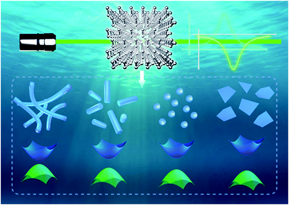 | ||
| Scheme 1 Schematic illustration of Te crystal structures and dimension-dependent nonlinear optical (NLO) properties. | ||
To investigate the impact of critical dimension shrinking, sophisticated material design is essential. In this study, we deliberately prepared the 1D and 0D Te nanomaterials with a constant diameter, so that the length of 1D Te nanomaterials becomes the only critical dimension. For the 2D Te nanosheets, their thickness was controlled to be smaller than the diameter of 1D and 0D nanomaterials, so that their critical dimension is further shrunk. As the critical dimensions were systematically reduced from 1D Te NWs, quasi 1D Te NRs and 0D Te NDs to 2D Te NSs, the electronic bandgaps were gradually widened, and the impact of critical dimension of Te nanomaterials on their NLO properties can be systematically investigated.
To prepare Te nanomaterials with well-controlled dimensions, we developed a cathodic electrochemical exfoliation method. Under cathodic electrochemical conditions, cation (such as H+) intercalation takes place in the space between these weakly bonded chains, which is driven by electrical fields. When electrons are received from the cathode, the subsequent H2 eruption could break the crystal and produce different nanoscale Te structures. Using this method, we successfully exfoliated bulk Te into uniform NWs, NRs and NDs, depending on the cation and pH values of the electrolyte as well as the applied bias voltages. The optimized experimental parameters and the corresponding production yields are summarized in the ESI.† Table S1 (ESI†) indicates that this novel cathodic electrochemical synthesis method gives very high productivity and excellent control over the morphology of Te nanomaterials. Meanwhile, Te NSs were obtained by a modified LPE process. The influence of different parameters such as the pretreatment process, types of solvents and sonication time on the efficiency of the exfoliation were also systematically studied and are summarized in Fig. S2–S4 (ESI†). We found that a ball-milling pretreatment followed by 3 h sonication in 2-butanol was the optimal condition to produce Te NSs. Under ultrasonication conditions, the exfoliation energy comes from the turbulence, shear forces, and cavitation bubbles within the Te suspension. When the energy is enough to overcome the vdW forces between the Te chains, Te NSs are formed as a result of the strong anisotropy of the bulk Te. These Te nanostructures with different critical dimensions were utilized in the following characterizations and NLO measurements.
Fig. 1a shows the high-angle annular dark-field (HAADF)-STEM image of Te NWs, and the bright field TEM image of Te NWs is shown in Fig. S5a (ESI†), revealing the ultralong 1D morphology with an average diameter of 9.4 ± 2.1 nm. Detailed diameter distributions are shown in Fig. S9a (ESI†). The corresponding elemental mappings in Fig. 1b and c show the uniformly dispersed Te element and negligible O element on the NWs. Energy dispersive spectroscopy (EDS) in Fig. S5b (ESI†) also shows that the NWs are predominantly composed of Te elements with a little content of oxygen. The above data confirm that the Te NWs are single crystals and the cathodic electrochemical exfoliation method can prevent Te from oxidation.
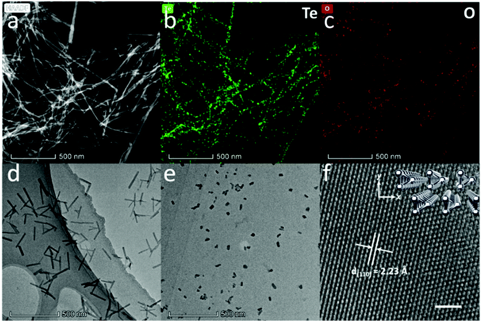 | ||
| Fig. 1 (a) High-angle annular dark-field (HAADF)-STEM image of Te NWs. (b and c) Elemental mapping of Te and O elements, respectively. (d) TEM image of Te NRs. (e) TEM image and (f) high-resolution TEM (HRTEM) image of Te NDs. Scale bar, 2 nm. Inset: the corresponding crystal structure. | ||
A representative TEM image of Te NRs is shown in Fig. 1d, while more TEM images are shown in Fig. S6a and b (ESI†). These quasi-1D Te nanostructures show uniform diameters of about 12.1 ± 2.8 nm (diameter distribution shown in Fig. S9b, ESI†) with length of about 200 nm. The SEM image and HAADF-STEM image of Te NRs are shown in Fig. S6c and d (ESI†). The elemental mapping in Fig. S6e and f (ESI†) indicates the majority of Te element with low oxygen content on the Te NR surface.
Fig. 1e shows the TEM image of Te NDs, while the additional TEM image and SEM image of Te NDs are shown in Fig. S7a and b (ESI†). These NDs exhibit typical 0D morphology with a uniform diameter of about 12.0 ± 3.0 nm (Fig. S9c, ESI†). High-resolution TEM (HRTEM) study in Fig. 1f reveals a clear atomic matrix with threefold-symmetry. The lattice spacing is measured to be 2.23 Å, corresponding to the (110) plane of trigonal Te. The inset of Fig. 1f shows the corresponding crystal structure, where each atomic triangle represents a single helical chain. Due to the weak vdW forces between the anisotropic chains, this kind of atomic arrangement can be hardly detected in other trigonal Te nanostructures.25–27 As shown above, we have obtained high quality Te NDs, NRs and NWs, and carefully controlled their diameter to be almost the same around 10 nm.
The TEM image of the Te NSs produced by the LPE method (Fig. 2a) shows the typical 2D morphology with sharp edges and corners, suggesting a good crystalline structure. These NSs are highly transparent to the electron beam, indicating the ultra-thin characteristic of the sample. The lateral size distributions are summarised in Fig. S9d (ESI†). Fig. 2b depicts the HRTEM of the Te NSs, showing the distinct rectangle-like atomic matrix, different from that of Te NDs shown in Fig. 1f. The lattice fringes are measured to be 1.98 Å, corresponding to the (003) plane of trigonal Te.26 As shown in the simulated crystal structure (inset of Fig. 2b), Te atomic chains are lying in the plane. Strong covalent bonds bind the neighboring two Te atoms forming the relatively stable (003) plane, making this crystal plane typical for trigonal Te. The selected area electron diffraction (SAED) pattern (Fig. 2c) displays a single set of diffraction spots, and the longitudinal (003) diffraction spot is consistent with the HRTEM results in Fig. 2b. SEM of the sample was also measured, and the results in Fig. S8 (ESI†) depict that these NSs were around 500 nm in lateral size with a smooth surface. Furthermore, the Te NS pieces were analyzed by atomic force microscopy (AFM) as shown in Fig. 2d. Several pieces of hundreds of nanometer scale NSs with similar surface contrast can be observed. From a typical height profile in the bottom of Fig. 2d, the NS thickness was measured to be 1.4–3.2 nm, corresponding to 3–7 layers – assuming the Te monolayer to be 0.45 nm.7 The thickness distributions can be found in Fig. S9e (ESI†). As a result, the 2D Te NSs were obtained with the critical dimension of 2.6 ± 0.6 nm, much lower than that of the Te NWs, NRs or NDs (about 10 nm).
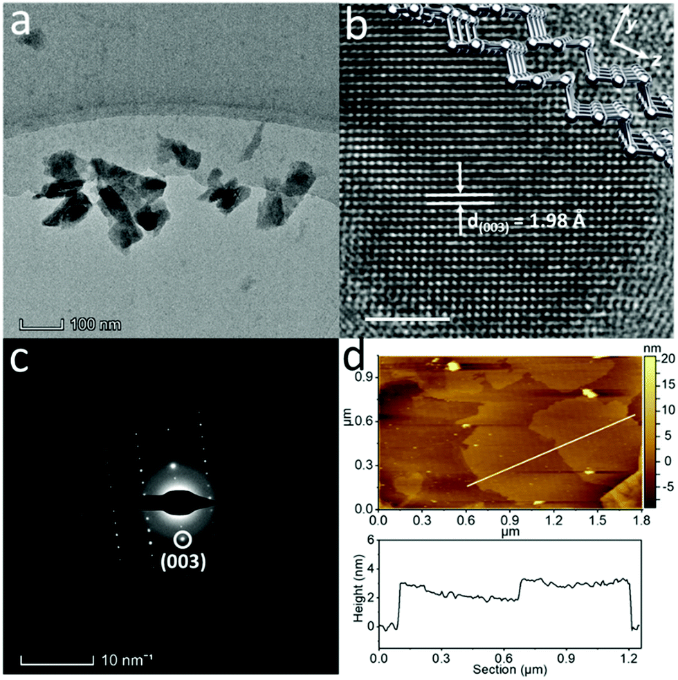 | ||
| Fig. 2 (a) TEM image and (b) HRTEM image of Te NSs. Inset: the simulated crystal structure. (c) The corresponding selected area electron diffraction (SAED) pattern. (d) Top: atomic force microscopy (AFM) image. Bottom: corresponding height profile of Te NSs. Scale bars, 2 nm (b); 10 nm−1 (c). | ||
The above microscopy results corroborated the systematic preparation of critical dimension-ranged Te nanostructures with structure integrity and single-crystallinity. Although these Te nanostructures were harvested under slightly different conditions, they were all composed of the unique Te atomic chains. The same atomic arrangement ensures that the evolution in physical or chemical properties should be mainly derived from the critical dimension effect.
Fig. 3a compares the absorption spectra of the four different Te nanostructures dispersed in NMP, which show broad absorption from 400 to 1000 nm. The broad absorption bands located at 695 nm, 622 nm and 573 nm for Te NWs, Te NRs and Te NDs, respectively, are attributed to the forbidden direction transitions.28 Such gradual blueshifts in the absorption from 695 nm for Te NWs to 573 nm for Te NDs indicate a bandgap evolution. The forbidden direction transition peak is hardly observed in Te NSs due to their very low thickness. Calculated from the Tauc plot in Fig. S10 (ESI†), the bandgap of Te nanostructures shows a steadily increasing trend from 1.12 eV for Te NWs, 1.28 eV for Te NRs and 1.39 eV for Te NDs to 2.0 eV for Te NSs, which is consistent with the literature.25,29,30 Previous works have suggested that the bandgap of 1D Te nanostructures would increase with the decrease of the aspect ratio.28 Here we controlled the diameter of the Te NWs, NRs and NDs to be the same value; therefore the gradual increase in the bandgap can be unambiguously attributed to the decrease in the length dimension. 2D Te NSs showed the highest bandgap of 2.0 eV, corresponding to the lowest critical dimension. That is to say, the lower critical dimension results in the wider bandgap of the Te nanostructures.
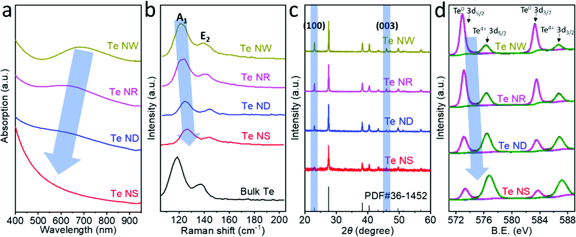 | ||
| Fig. 3 (a) Absorption spectra of the Te nanostructures in NMP. (b) Raman spectra of the Te nanostructures compared with that of bulk Te. (c) X-ray diffraction (XRD) patterns of the Te nanostructures and the standard PDF card. (d) X-ray photoelectron spectroscopy (XPS) spectra of the Te nanostructures. | ||
Fig. 3b compares the Raman characterizations of the Te nanostructures with that of the bulk Te. Bulk trigonal Te exhibits two characteristic Raman modes, A1 and E2, located at 119.4 cm−1 and 139.5 cm−1, corresponding to chain expansion and bond-stretching, respectively.9 The A1 modes were observed at 121.0, 122.7, 124.3 and 126.2 cm−1 for Te NWs, NRs, NDs and NSs, respectively, showing a gradual shift to higher wavenumbers. The higher Raman active modes result from the enhancement of covalent interactions within the chain and weakening of vdW forces between the chains, consistent with the decreases of the critical dimensions. Such Raman shifts have also been observed previously in few-chain Te9 and few-layer Te.7 In addition, the Raman shifts of A1 mode for Te NWs, NRs, NDs and NSs are 1.6, 3.3, 4.9 and 6.8 cm−1, respectively, which are higher than those of E2 mode (1.0, 2.0, 4.4 and 5.1 cm−1 for Te NWs, NRs, NDs and NSs, respectively). Previous studies showed that the long-range Coulombic interactions dominate the vibration mode of the individual Te atomic chains in the few-chain samples.9 The chain expansion may be more strongly affected by the long-range Coulombic interactions than by bond-stretching due to the high anisotropy, resulting in the more significant Raman shifts of A1 than E2 vibration mode. Similar differences in Raman shifts are also theoretically predicted and experimentally observed in the studies based on black phosphorus.31,32
Fig. 3c shows the X-ray diffraction (XRD) pattern evolution of the Te nanostructures and the standard PDF card. The (100) and (003) facets of trigonal Te are located at 23.1° and 45.9°, respectively, which are the typical peaks showing the crystal direction of Te nanomaterials. These two peaks exhibited a gradual increase for 0D Te NDs to 1D Te NRs and NWs, indicating the strong anisotropy of trigonal Te and the growth direction of 1D Te nanostructures mainly along the [100] and [001] zone axes. The 2D Te NSs exhibited the lowest (100) and (003) peaks, showing the successful exfoliation of the trigonal Te by the LPE process.33 Moreover, compared with Te NWs, NRs and NDs, the 2D Te NSs show negligible (003) facets. It can be deduced that the exfoliation occurred along the c-axis to form the 2D Te NSs and the critical dimension of 2D Te is mainly along the c-axis of the crystal.
High-resolution X-ray photoelectron spectroscopy (XPS) spectra of these four Te nanostructures are shown in Fig. 3d. The Te 3d5/2 and 3d3/2 peaks of Te nanostructures can be deconvoluted into two peaks,34 and the components of the binding energies obtained by fitting analysis are summarized in Table 1. Te NWs exhibited predominant Te0 content (79.90%) and slight oxide (TeO2) content (20.10%). The oxide (TeO2) content gradually increases to 30.48% for Te NRs, 57.80% for Te NDs and 73.93% for Te NSs. In addition, the peak position of Te4+ 3d5/2 shifts from 576.27 eV (Te NWs), 576.33 eV (Te NRs), and 576.41 eV (Te NDs) to 576.79 eV (Te NSs). Consistent peak position shifts are also observed for Te4+ 3d3/2, Te0 3d5/2 and Te0 3d3/2 peaks. Such binding energy shifts can also be attributed to the increased oxide (likely TeO2) content resulting in the reduced electron density, reducing the shielding effect. The main reasons for such an increase of surface oxidation with reduction of critical dimension can be attributed to two facts. First, as the critical dimensions decrease, that is from Te NWs, NRs and NDs to NSs, the ratio of the surface atoms increases significantly. Moreover, unlike the 1D Te nanomaterials fabricated by the cathodic exfoliation method that was under an essentially electrochemical reducing condition,34 the 2D Te nanosheets prepared by the LPE method were exposed to oxygen under ultrasonication, leading to more obvious surface oxidation, which is common for the fabrication of 2D materials by LPE.33,35–37
| Te0 3d5/2 | Te4+ 3d5/2 | Te0 3d3/2 | Te4+ 3d3/2 | |||||
|---|---|---|---|---|---|---|---|---|
| B.E. (eV) | Conc. (%) | B.E. (eV) | Conc. (%) | B.E. (eV) | Conc. (%) | B.E. (eV) | Conc. (%) | |
| Te NDs | 573.17 | 24.66 | 576.41 | 35.00 | 583.54 | 17.54 | 586.80 | 22.80 |
| Te NRs | 573.15 | 42.49 | 576.33 | 19.97 | 583.51 | 27.03 | 586.73 | 10.51 |
| Te NWs | 572.93 | 49.61 | 576.27 | 13.62 | 583.29 | 30.29 | 586.67 | 6.48 |
| Te NSs | 573.35 | 15.45 | 576.79 | 44.97 | 583.73 | 10.62 | 587.14 | 28.96 |
The NLO properties of these Te nanostructures were investigated through a femtosecond (fs) open-aperture Z-scan technique. NMP was utilized as the medium for the following NLO measurements, because it displays no NLO signal and the high boiling point nature minimizes the thermal effects from the ultrafast laser.38 The resulting Z-scan curves are normalized transmittance as a function of the sample position. The Z-scan data were fitted to the nonlinear transmission equation:
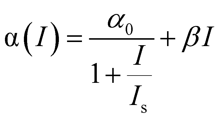 | (1) |
The fs Z-scan measurements of these Te nanostructures dispersed in NMP in 2 mm optical length quartz cells were conducted under the incident laser wavelength of 600 nm (Fig. 4), where these samples exhibited the broadband absorption. Pure NMP in the same quartz cells was measured and showed no NLO signals. Fig. 4a summarizes the NLO behavior of the Te NWs under increasing intensity. Significant SA behavior was detected under low laser energy of 280 nJ. However, when the laser intensity gradually increases to 1050 nJ and further to 1480 nJ, slightly reverse saturable absorption (RSA) around the focus (Z = 0 mm) gradually appears and then increases. Subtler Z-scan measurements under different laser intensities are also tested and collected in Fig. S11a (ESI†), showing strong intensity-dependent NLO properties transitioning from SA to RSA. Moreover, when the laser intensity finally changed back to 280 nJ, the SA signal (shown in Fig. S11b, ESI†) showed excellent resemblance to the results in Fig. 4a, indicating that the Te nanostructures can sustain the high intensity laser with no obvious damage. Similar intensity-dependent SA to RSA NLO properties have been previously reported in molybdenum sulfide (MoS2),39 black phosphorus (BP),40,41 antimony (Sb) NSs42,43 and other materials.44
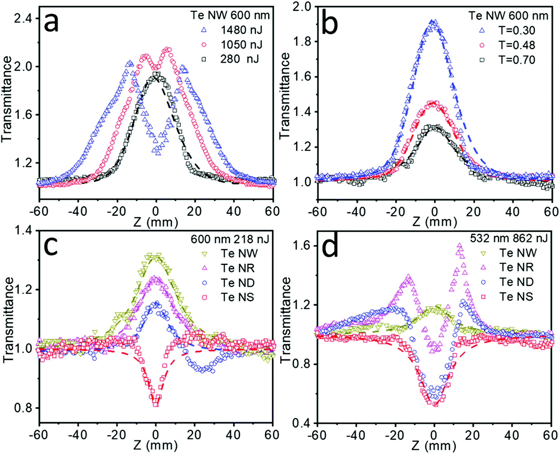 | ||
| Fig. 4 Femtosecond (fs) open-aperture Z-scan results of the Te nanostructures. (a) Experimental results of Te NWs under laser power of 280, 1050 and 1480 nJ (600 nm). (b) Experimental results of Te NWs with the sample transmittance of 0.70, 0.48 and 0.30. (c) Experimental results of dimension-ranged Te nanostructures for 600 nm. Dashed lines: fitted Z-scan curves. (d) Experimental results of dimension-ranged Te nanostructures for 532 nm. Dashed lines: fitted Z-scan curves. | ||
In general, Pauli blocking resulting from the narrow bandgap may lead to long exciton bleaching and SA behavior,45 while the RSA is usually explained as the two-photon absorption (TPA)40 or excited state absorption (ESA).44 Under our experimental conditions, the bandgap of Te nanostructures shows a steady increase from 1.12 eV for Te NWs, 1.28 eV for Te NRs, and 1.39 eV for Te NDs to 2.0 eV for Te NSs (Fig. S10, ESI†). As the band gaps of these Te nanostructures are lower than the used photon energy (2.07 eV), TPA can be excluded here. The intensity-dependent NLO properties of the Te nanostructures can be explained as the result of competition between exciton bleaching and ESA under the influence of laser intensity.46 Under low laser intensity, bleaching of the ground state absorption of these Te nanostructures was dominant, thus showing the SA signal. When the intensity rises, ESA becomes dominant and the RSA behavior appears and increases gradually.
Meanwhile, apart from intensity-dependent NLO properties, a strong transmittance-dependent NLO behavior is also observed form Fig. 4b. Te NWs were tested at a fixed laser intensity of 280 nJ with the transmittance decreasing from 0.70, to 0.48, to 0.30, resulting in a steady increase in SA behavior. Fitting these results by eqn (1), the increased nonlinear absorption coefficient β values (Table S2, ESI†) are also obtained as the transmittance decreased. The increased β values illustrate that the stronger SA behavior in the lower transmittance is not resulted from simple addition of the SA signals. For nanomaterials with high absorption cross sections and a small curvature radius, the laser-induced heating could lead to solvent evaporation and micro-bubble formation around the nanomaterial, further causing thermally induced nonlinear scattering with the appearance of RSA.38 Even though an fs laser and a high boiling point solvent could greatly weaken this thermal effect, it may still exist in liquid phase Z-scan tests. The higher the transmittance of the sample, the higher the solvent concentration, therefore leading to severe thermally induced RSA and a lower β value. This transmittance-dependent NLO behavior is also detected in Te NRs and ND materials, the results are shown in Fig. S12a and b (ESI†), respectively.
Importantly, it is found that the observed NLO properties exhibit strong dependence on the dimension of these Te nanostructures. As shown in Fig. 4c, the Te NWs exhibited a stronger SA behavior than Te NRs, while Te NDs showed SA accompanying RSA signals, and Te NSs exhibited strong RSA behavior under the same laser intensity and sample transmittance. The above results indicate that as the critical dimension decreases, the NLO properties gradually change from SA to RSA behavior. 0D Te nanoparticles have been previously proven to show superior optical nonlinearity to graphene.16 Here 1D Te NWs and quasi-1D Te NRs exhibited even higher SA behavior than the 0D Te nanostructure, indicating promising applications in the field of ultrafast nonlinear optics. Moreover, Table 2 summarizes the NLO parameters observed for the 1D Te NWs, quasi-1D Te NRs and 0D Te NDs in this work, and the typical nanomaterials with the SA behavior reported in the literature, including BP NDs,41 BP NSs,41,46–49 Sb NSs,42 molybdenum telluride (MoTe2) NSs44 and bismuth (Bi) NSs.32 The highest β values (even with a quite high transmittance of 0.70) of Te NWs, NRs and NDs obtained in this work indicate the superior SA behavior for our Te nanomaterials. Due to the superior SA properties, 1D Te nanomaterials can be utilized as a saturable absorber for ultrafast pulse laser generation. With the ultra-high β value, the energy loss of the laser transmitting through the materials may be reduced to a very low level, resulting in high peak intensity.
| Materials | T (%) | Laser | β (m W−1) | Ref. |
|---|---|---|---|---|
| BP NDs | 69.8 | 800 nm, 1 kHz, 60 fs | −7.78 ± 0.4 × 10⁻¹³ | 41 |
| BP NSs | 76.1 | 800 nm, 1 kHz, 60 fs | −2.88 ± 0.06 × 10⁻¹³ | 41 |
| BP NSs | 61.1 | 532 nm, 6 ns | −1.00 × 10⁻⁹ | 46 |
| BP NSs | 68 | 800 nm, 1 kHz, 100 fs | −7.21 ± 0.23 × 10⁻¹⁴ | 47 |
| BP NSs | 55.3 | 1972 nm, 50 kHz | −1.00 ± 0.028 × 10⁻¹² | 48 |
| BP NSs | 74.3 | 515 nm | −2.66 ± 0.29 × 10⁻¹³ | 49 |
| Sb NSs | 70.0 | 532 nm, 10 Hz, ∼4 ns | −4.5 × 10⁻¹⁰ | 42 |
| MoTe2 NSs | 85.1 | 800 nm, 1 kHz, 35 fs | −1.28 × 10⁻⁹ | 44 |
| Bi NSs | 70.0 | 1064 nm, 10 Hz, ∼4 ns | −3.9 × 10⁻¹⁰ | 32 |
| Te NWs | 70.0 | 600 nm, 1 kHz, <110 fs | −8.3 ± 3.6% × 10−9 | This work |
| Te NRs | 70.0 | 600 nm, 1 kHz, <110 fs | −6.7 ± 3.9% × 10−9 | This work |
| Te NDs | 70.0 | 600 nm, 1 kHz, <110 fs | −3.5 ± 2.2% × 10−9 | This work |
The NLO behavior of nanomaterials can be affected by several factors, such as particle size,38,42 defects,50 temperature,41 chemical composition51 and bandgaps.49 Under our experimental conditions, the Te NWs showed higher SA behavior than the other samples, which can be explained by the stronger Pauli blocking effects due to their smaller bandgap. More importantly, 2D Te NSs are demonstrated to be an optical limiting material in the fs timescale for the first time. The Z-scan experiments of dimension-ranged Te nanostructures were also conducted under a 532 nm laser pulse with the same laser intensity and sample transmittance (Fig. 4d), indicating similar dimension-dependent NLO properties transitioning from the SA to RSA behavior. The detailed parameters associated with NLO properties of Te NSs and other nanomaterials with RSA behavior, including BP NSs,41,46,52 Sb NSs,42,43 MoTe2 NSs,44 WS2 NDs,53 graphene (G) NSs,54 graphene oxide (GO) NSs55 and boron nitride (BN) NSs56 are also summarized in Table 3. The largest β values (even with a quite high transmittance of 0.70) of 2D Te NSs shows superior optical limiting properties compared with the literature-reported materials. In practical applications, the RSA property with high β value will result in strong capability to cut off laser power, while maintaining high linear transmittance at the same time in the laser protection areas.
| Materials | T (%) | Laser | β (m W−1) | Ref. |
|---|---|---|---|---|
| BP NDs | 77.5 | 1550 nm, 1kHz, 65fs | 4.39 ± 0.15 × 10⁻¹³ | 41 |
| BP NSs | 55.6 | 532 nm, 6 ns | 2.08 × 10⁻⁹ | 46 |
| BP NSs | 31.0 | 532 nm, 30 ps | 1.6 × 10⁻¹⁰ | 52 |
| Sb NSs | 70 | 532 nm, ∼4 ns | 1.05 × 10⁻¹⁰ | 42 |
| Sb NSs | 77.2 | 532 nm, 30 ps | 4.3 × 10⁻¹² | 43 |
| MoTe2 NSs | 85.1 | 800 nm, 1 kHz, 35 fs | 1.73 × 10⁻⁹ | 44 |
| WS2 NDs | 48 | 532 nm, 8 ns | 1.56 × 10⁻⁹ | 53 |
| G NSs | — | 532 nm, 40 ps | 4.6 × 10⁻¹² | 54 |
| GO NSs | 11 | 532 nm, 35 ps | 3.7 × 10⁻¹² | 55 |
| BN NSs | 7.65 | 532 nm, 30 ps | 7.9 × 10⁻¹³ | 56 |
| Te NSs | 70.0 | 532 nm, 1 kHz, <110 fs | 9.0 ± 4.3% × 10−9 | This work |
| Te NSs | 70.0 | 600 nm, 1 kHz, <110 fs | 3.1 ± 1.1% × 10−9 | This work |
Based on our investigation and previous literature, the morphology factors including the length and diameter will affect the NLO behavior. The sizes of nanomaterials will affect the bandgap due to the quantum confinement effect. Meanwhile, 1D Te NWs and 0D Te NDs with different lengths and diameters have different ratios of surface atoms, affecting the surface oxidation and defects. In this work, to avoid complication of data analysis and unveil the key factor affecting the NLO properties, we deliberately controlled the diameters of 1D Te NWs and 0D Te NDs to be the same. Under such conditions, our investigations revealed that the key factor influencing the NLO behavior of Te nanostructures is the critical dimension. Therefore, our work focuses on the dimension-dependence of the NLO properties.
It is known that some materials in the solid state will show different nonlinear properties compared with those in suspensions. One phenomenon is known as the solvent effect, especially in the solvents with low boiling points. When low boiling point solvents are used, nonlinear scattering formed by the laser-induced solvent bubbles will dominante the NLO properties, resulting in apparent optical limiting behavior.57–59 To avoid such solvent effects, we choose the high boiling point NMP as the dispersion solvent, which is known to have low bubble effect under our experimental conditions. To confirm the dimension-dependent NLO properties, the fs Z-scan measurements of polymethyl methacrylate (PMMA) thin film blended with Te NWs, NRs, NDs and NSs were conducted. Under laser intensities of 233 nJ and 467 nJ (results shown in Fig. S13a and b, ESI†), transition of the NLO properties from SA to RSA behavior was detected as the film samples were changed from Te NWs, NRs, and NDs to NSs. When the laser intensities increased to 644 nJ and 1040 nJ (Fig. S13c and d, ESI†), all the films exhibited RSA behavior. These dimension- and intensity-dependent NLO properties of Te/PMMA films are similar to those observed in their NMP dispersions, verifying the excellent intrinsic NLO properties of these Te nanomaterials and the potential applications as solid films in the field of ultrafast mode-lockers or laser protection.
The photo-induced NLO properties are tightly related to electron excited-state dynamics of the Te nanostructures; thus fs transient absorption (TA) spectra were obtained to investigate the ultrafast exciton dynamics. Fig. 5 displays the bird's eye plot (wavelength vs. time vs. intensity) of the TA spectra for the different Te nanostructures, showing two obvious signals in the spectral range of 450 nm to 800 nm. Pure NMP and tellurium oxide were also tested and showed no detectable signals. The ESA signal located between 600 nm and 800 nm is on the fs to several ps timescale, corresponding to the fast intraband thermalization,60,61 while the long exciton bleaching signal located between 450 nm and 650 nm indicates the slower electron–hole recombination process.32 These two signals reveal the possible relaxation channels of the photo-generated carriers.
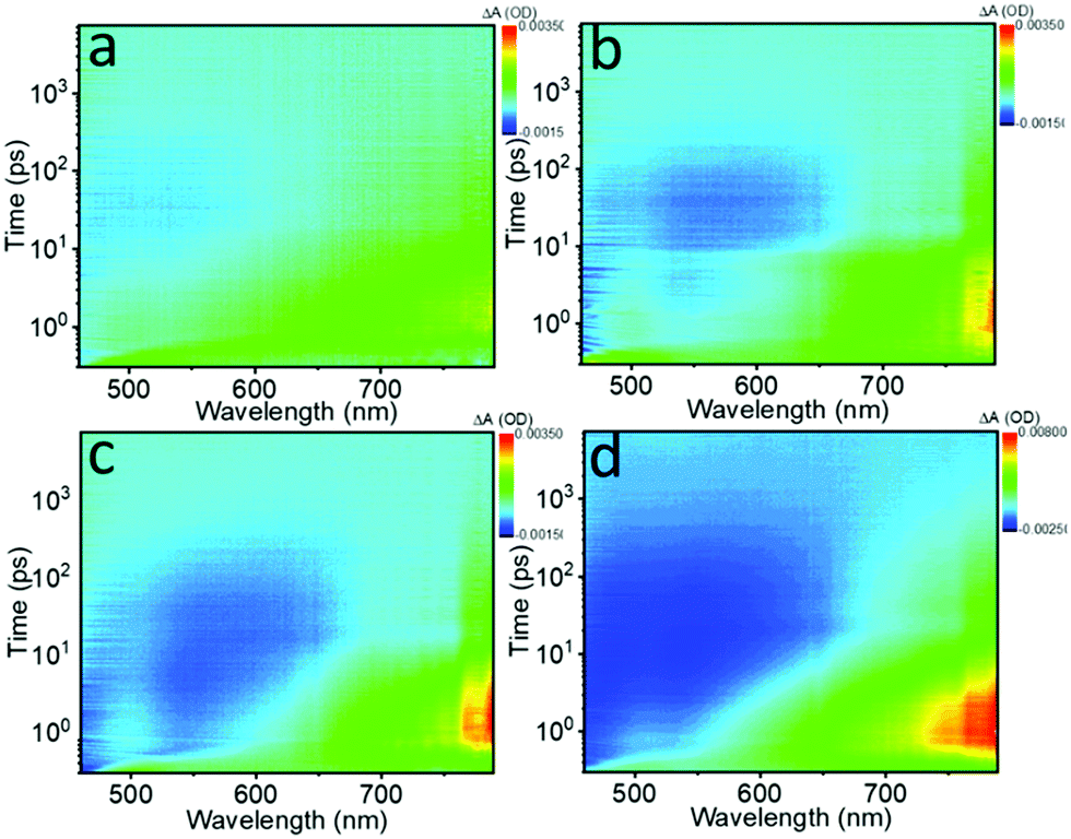 | ||
| Fig. 5 Bird's eye plots of fs transient absorption (TA) spectra of the (a) Te NWs, (b) Te NRs, (c) Te NDs and (d) Te NSs in NMP solvent pumped at 400 nm (1.0 μJ), respectively. | ||
To extract the detailed lifetime components, the decay curves recorded at ∼780 nm were fitted in Fig. S14 (ESI†) and the results are collected in Table 4. Three lifetime components can be extracted for all the samples. The first two lifetimes (τ1 and τ2) are in good agreement with the two signals shown in the bird's eye plots, which decrease gradually as the critical dimension decreases. Moreover, the fitting results here also exhibit a long ns component exceeding the 7 ns time window for the fs TA spectra in all of the samples, indicating the existence of a long exciton bleaching time up to the μs timescale. With the decrease of the critical dimensions, the ns component is decreased from 7.2%, 5.0%, and 4.1% to 0.9%, respectively.
| Wavelength (nm) | τ 1 (ps) | τ 2 (ps) | τ 3 > 7 ns | |
|---|---|---|---|---|
| Te NWs | 780 | 8.52 ± 0.91 (70.4%) | 389 ± 72.1 (22.5%) | −7.2% |
| Te NRs | 780 | 8.39 ± 0.89 (78.1%) | 291 ± 55.3 (17.0%) | −5.0% |
| Te NDs | 780 | 7.34 ± 0.66 (72.3%) | 261 ± 38.4 (23.5%) | −4.1% |
| Te NSs | 780 | 6.77 ± 0.41 (66.5%) | 242 ± 20.1 (33.5%) | −0.9% |
Based on the fs TA spectra and the fitting data, the carrier dynamic processes and the evolutions of the NLO behavior are summarized in Fig. 6. Upon photoexcitation, photogenerated excitons are formed on the fs scale. When the pump intensity is strong enough to generate abundant electrons and holes to fill the conduction band (CB) and valence band (VB) edges, respectively, further photo-absorption is prevented as a result of Pauli blocking, resulting in the observed SA behavior.48,60 In general, this Pauli blocking can be reflected by the long exciton bleaching in the TA spectra.32 Compared to the quasi-1D Te NRs (1.28 eV) and 0D Te NDs (1.39 eV), 1D Te NWs show the smallest bandgap of 1.12 eV. Thus, under the same pump laser irradiation, the photogenerated carriers can easily fill the CB and VB edges, as confirmed by the highest ns component (τ3) in the fitting results, further showing the strongest SA behavior. The 1D Te NWs exhibited the lowest oxygen content (Fig. 3d and Table 1), indicating that the ideal Te nanostructures with the highest critical dimension would show the strongest SA behavior. As the critical dimension decreases, the increasing bandgap makes Pauli blocking more difficult; consequently the quasi-1D Te NRs and 0D Te NDs show gradually decreasing ns components (τ3) and SA signals. Moreover, the decreased critical dimension also leads to the increase of the oxide content and trap states. These trap and edge states can act as a “springboard” to help the electrons transfer to higher levels, that is to say, inducing ESA signals.38,62 Such increased ESA signals, confirmed by the TA spectra range of 650 nm to 800 nm in Fig. 5a–c, gradually brought about the increasing RSA behavior (Fig. 4d).
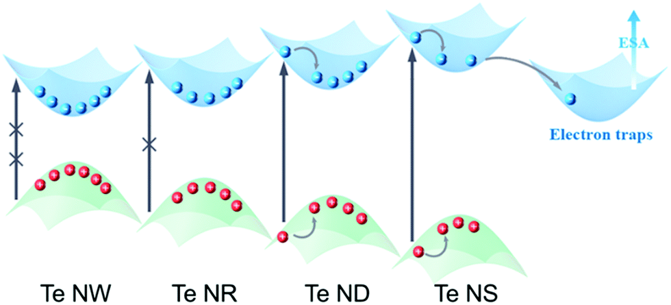 | ||
| Fig. 6 Schematic NLO mechanism of Te NWs, NRs, NDs and NSs, respectively. | ||
However, for 2D Te NSs, the lowest critical dimension and ultra large lateral sizes brought about relatively high oxide contents (Fig. 3d and Table 1), which further increased the trap states compared with 1D and 0D Te nanomaterials. These widely distributed trap levels can provide greater probability for ESA (evidenced by the fs TA spectra in Fig. 5d and the decay curves in Fig. S14, ESI†); thus strong RSA signal is observed. Recent studies have shown that the trap and edge states do significantly enhance the RSA behavior of MoS2,38 tungsten disulfide (WS2),53 BP47 and Sb NSs.42 As a result, Te nanostructures exhibited critical dimension-dependent faster exciton dynamics and stronger ESA, which were responsible for the RSA behavior of 2D Te NSs.
Conclusions
In conclusion, Te nanostructures with systematically reduced critical dimensions were harvested, including 1D Te NWs, quasi-1D Te NRs, 0D Te NDs and 2D Te NSs by cathodic exfoliation and LPE. The fs Z-scan measurements performed on these Te nanostructures revealed the strong power-, transmittance- and dimension-dependence of the NLO behavior. As the critical dimension reduces, the NLO properties showed a transition from strong SA to strong RSA behavior. 0D Te nanoparticles have been previously proven to show superior optical nonlinearity than graphene. Herein, we demonstrate that 1D Te NWs and quasi-1D Te NRs exhibited even higher SA behavior than 0D Te nanostructures, indicating promising applications in the field of ultrafast nonlinear optics. Moreover, the 2D Te NSs are demonstrated to be a high-performance optical limiting material, which further broadens the applications of 2D Te to laser protection and other novel ultrafast photonics. TA analysis revealed that the RSA behavior of 2D Te NSs is derived from faster exciton relaxation and stronger ESA behavior than other Te nanostructures. The results in this work provide clear guideline to control the NLO properties of Te nanostructures and bring a further understanding on the evolution of optical properties on their dimensions.Author contributions
H. L. Zhang, Q. Xiao conceived the idea for the manuscript and designed the experiments. Q. Xiao synthesized the materials and conducted the characterization experiments. Q. Xiao conducted the Z-scan measurements. Q. Xiao, B. Ma and X. P. Zhai carried out the fitting analysis of the Z-scan data. B. Ma obtained the fs TA spectra. Q. Xiao, X. Fei and B. Ma analyzed the TA results. D. W. Liu, X. Y. Li and M. J. Xiao discussed the characterization results. H. L. Zhang, Q. Wang and Y. Peng discussed the results and commented on the manuscript at all stages. H. L. Zhang led the project.Conflicts of interest
The authors declare no competing financial interest.Acknowledgements
This work was supported by the Ministry of Science and Technology of China (2017YFA0204903), the National Natural Science Foundation of China (51733004, 51525303, 22073038, and 61675129), the 111 Project, and the Fundamental Research Funds for the Central Universities. The authors wish to thank the Electron Microscopy Center of Lanzhou University for the microscopy and microanalysis of the specimens.Notes and references
- K. S. Novoselov, A. Mishchenko, A. Carvalho and A. H. Castro Neto, Science, 2016, 353, aac9439 CrossRef CAS PubMed.
- E. J. Reed, Nature, 2017, 552, 40 CrossRef CAS PubMed.
- Y. Liu, W. Wu and W. A. Goddard, 3rd, J. Am. Chem. Soc., 2018, 140, 550 CrossRef CAS PubMed.
- Z. Zhu, X. Cai, S. Yi, J. Chen, Y. Dai, C. Niu, Z. Guo, M. Xie, F. Liu, J. H. Cho, Y. Jia and Z. Zhang, Phys. Rev. Lett., 2017, 119, 106101 CrossRef PubMed.
- M. Hirayama, R. Okugawa, S. Ishibashi, S. Murakami and T. Miyake, Phys. Rev. Lett., 2015, 114, 206401 CrossRef PubMed.
- G. Qiu, C. Niu, Y. Wang, M. Si, Z. Zhang, W. Wu and P. D. Ye, Nat. Nanotechnol., 2020, 15, 585 CrossRef CAS PubMed.
- Y. Wang, G. Qiu, R. Wang, S. Huang, Q. Wang, Y. Liu, Y. Du, W. A. Goddard, M. J. Kim, X. Xu, P. D. Ye and W. Wu, Nat. Electron., 2018, 1, 228 CrossRef.
- C. Zhao, C. Tan, D. H. Lien, X. Song, M. Amani, M. Hettick, H. Y. Y. Nyein, Z. Yuan, L. Li, M. C. Scott and A. Javey, Nat. Nanotechnol., 2020, 15, 53 CrossRef CAS PubMed.
- J.-K. Qin, P.-Y. Liao, M. Si, S. Gao, G. Qiu, J. Jian, Q. Wang, S.-Q. Zhang, S. Huang, A. Charnas, Y. Wang, M. J. Kim, W. Wu, X. Xu, H.-Y. Wang, L. Yang, Y. Khin Yap and P. D. Ye, Nat. Electron., 2020, 3, 141 CrossRef CAS.
- D. Dini, M. J. F. Calvete and M. Hanack, Chem. Rev., 2016, 116, 13043 CrossRef CAS PubMed.
- U. Keller, Nature, 2003, 424, 831 CrossRef CAS PubMed.
- A. Autere, H. Jussila, Y. Dai, Y. Wang, H. Lipsanen and Z. Sun, Adv. Mater., 2018, 30, 1705963 CrossRef PubMed.
- X. P. Zhai, B. Ma, Q. Wang and H. L. Zhang, Phys. Chem. Chem. Phys., 2020, 22, 22140 RSC.
- L. Wu, W. Huang, Y. Wang, J. Zhao, D. Ma, Y. Xiang, J. Li, J. S. Ponraj, S. C. Dhanabalan and H. Zhang, Adv. Funct. Mater., 2019, 29, 1806346 CrossRef.
- F. Zhang, G. Liu, Z. Wang, T. Tang, X. Wang, C. Wang, S. Fu, F. Xing, K. Han and X. Xu, Nanoscale, 2019, 11, 17058 RSC.
- K. Wang, X. Zhang, I. M. Kislyakov, N. Dong, S. Zhang, G. Wang, J. Fan, X. Zou, J. Du, Y. Leng, Q. Zhao, K. Wu, J. Chen, S. M. Baesman, K.-S. Liao, S. Maharjan, H. Zhang, L. Zhang, S. A. Curran, R. S. Oremland, W. J. Blau and J. Wang, Nat. Commun., 2019, 10, 3985 CrossRef PubMed.
- P. Mohanty, T. Kang, B. Kim and J. Park, J. Phys. Chem. B, 2006, 110, 791 CrossRef CAS PubMed.
- C. J. Hawley, B. R. Beatty, G. Chen and J. E. Spanier, Cryst. Growth Des., 2012, 12, 2789 CrossRef CAS.
- Q. Lu, F. Gao and S. Komarneni, Adv. Mater., 2004, 16, 1629 CrossRef CAS.
- J. Yuan, H. Schmalz, Y. Xu, N. Miyajima, M. Drechsler, M. W. Möller, F. Schacher and A. H. E. Müller, Adv. Mater., 2008, 20, 947 CrossRef CAS.
- H. Yang, S. W. Finefrock, J. D. Albarracin Caballero and Y. Wu, J. Am. Chem. Soc., 2014, 136, 10242 CrossRef CAS PubMed.
- W. Huang, Y. Huang, Y. You, T. Nie and T. Chen, Adv. Funct. Mater., 2017, 27, 1701388 CrossRef.
- Y.-J. Zhu, W.-W. Wang, R.-J. Qi and X.-L. Hu, Angew. Chem., Int. Ed., 2004, 43, 1410 CrossRef CAS PubMed.
- J. R. Reitz, Phys. Rev., 1957, 105, 1233 CrossRef CAS.
- Z. Xie, C. Xing, W. Huang, T. Fan, Z. Li, J. Zhao, Y. Xiang, Z. Guo, J. Li, Z. Yang, B. Dong, J. Qu, D. Fan and H. Zhang, Adv. Funct. Mater., 2018, 28, 1705833 CrossRef.
- J. W. Liu, J. H. Zhu, C. L. Zhang, H. W. Liang and S. H. Yu, J. Am. Chem. Soc., 2010, 132, 8945 CrossRef CAS PubMed.
- J. Peng, Y. Pan, Z. Yu, J. Wu, J. Wu, Y. Zhou, Y. Guo, X. Wu, C. Wu and Y. Xie, Angew. Chem., Int. Ed., 2018, 57, 13533 CrossRef CAS PubMed.
- J.-W. Liu, J. Xu, W. Hu, J.-L. Yang and S.-H. Yu, ChemNanoMat, 2016, 2, 167 CrossRef CAS.
- W. Huang, Y. Zhang, Q. You, P. Huang, Y. Wang, Z. N. Huang, Y. Ge, L. Wu, Z. Dong, X. Dai, Y. Xiang, J. Li, X. Zhang and H. Zhang, Small, 2019, 15, 1900902 CrossRef PubMed.
- T. Yang, H. Ke, Q. Wang, Y. Tang, Y. Deng, H. Yang, X. Yang, P. Yang, D. Ling, C. Chen, Y. Zhao, H. Wu and H. Chen, ACS Nano, 2017, 11, 10012 CrossRef CAS PubMed.
- Y. Feng, J. Zhou, Y. Du, F. Miao, C. G. Duan, B. Wang and X. Wan, J. Phys.: Condens. Matter, 2015, 27, 185302 CrossRef PubMed.
- Q. Q. Yang, R. T. Liu, C. Huang, Y. F. Huang, L. F. Gao, B. Sun, Z. P. Huang, L. Zhang, C. X. Hu, Z. Q. Zhang, C. L. Sun, Q. Wang, Y. L. Tang and H. L. Zhang, Nanoscale, 2018, 10, 21106 RSC.
- X. Wang, J. He, B. Zhou, Y. Zhang, J. Wu, R. Hu, L. Liu, J. Song and J. Qu, Angew. Chem., Int. Ed., 2018, 57, 8668 CrossRef CAS PubMed.
- Q. Xiao, X. Y. Li, Z. Q. Zhang, C. X. Hu, G. H. Dun, B. Sun, Y. Peng, Q. Wang, Z. Zheng and H. L. Zhang, Adv. Electron. Mater., 2020, 6, 2000240 CrossRef CAS.
- J. Gu, Z. Du, C. Zhang, J. Ma, B. Li and S. Yang, Adv. Energy Mater., 2017, 7, 1700447 CrossRef.
- R. Gusmao, Z. Sofer, D. Bousa and M. Pumera, Angew. Chem., Int. Ed., 2017, 56, 14417 CrossRef CAS PubMed.
- C.-X. Hu, Q. Xiao, Y.-Y. Ren, M. Zhao, G.-H. Dun, H.-R. Wu, X.-Y. Li, Q.-Q. Yang, B. Sun, Y. Peng, F. Yan, Q. Wang and H.-L. Zhang, Adv. Funct. Mater., 2018, 28, 1805311 CrossRef.
- K. G. Zhou, M. Zhao, M. J. Chang, Q. Wang, X. Z. Wu, Y. Song and H. L. Zhang, Small, 2015, 11, 694 CrossRef CAS PubMed.
- Q. Ouyang, H. Yu, K. Zhang and Y. Chen, J. Mater. Chem. C, 2014, 2, 6319 RSC.
- X. Zheng, R. Chen, G. Shi, J. Zhang, Z. Xu, X. Cheng and T. Jiang, Opt. Lett., 2015, 40, 3480 CrossRef CAS PubMed.
- R. Chen, X. Zheng and T. Jiang, Opt. Express, 2017, 25, 7507 CrossRef CAS PubMed.
- L. Zhang, S. Fahad, H. R. Wu, T. T. Dong, Z. Z. Chen, Z. Q. Zhang, R. T. Liu, X. P. Zhai, X. Y. Li, X. Fei, Q. W. Song, Z. J. Wang, L. C. Chen, C. L. Sun, Y. Peng, Q. Wang and H. L. Zhang, Nanoscale Horiz., 2020, 5, 1420 RSC.
- F. Zhang, M. Wang, Z. Wang, K. Han, X. Liu and X. Xu, J. Mater. Chem. C, 2018, 6, 2848 RSC.
- C. Quan, M. He, C. He, Y. Huang, L. Zhu, Z. Yao, X. Xu, C. Lu and X. Xu, Appl. Surf. Sci., 2018, 457, 115 CrossRef CAS.
- H. Yu, H. Zhang, Y. Wang, C. Zhao, B. Wang, S. Wen, H. Zhang and J. Wang, Laser Photonics Rev., 2013, 7, L77 CrossRef CAS.
- K. Wang, N. Dong, Z. Liu, M. Shi, B. Zhang, J. Wang and Y. Chen, Polym. Chem., 2019, 10, 6003 RSC.
- Y. Xu, X.-F. Jiang, Y. Ge, Z. Guo, Z. Zeng, Q.-H. Xu, H. Zhang, X.-F. Yu and D. Fan, J. Mater. Chem. C, 2017, 5, 3007 RSC.
- K. Wang, B. M. Szydlowska, G. Wang, X. Zhang, J. J. Wang, J. J. Magan, L. Zhang, J. N. Coleman, J. Wang and W. J. Blau, ACS Nano, 2016, 10, 6923 CrossRef CAS PubMed.
- S. Zhang, X. Zhang, H. Wang, B. Chen, K. Wu, K. Wang, D. Hanlon, J. N. Coleman, J. Chen, L. Zhang and J. Wang, Opt. Mater. Express, 2016, 6, 3159 CrossRef CAS.
- X. Zhang, S. Zhang, Y. Xie, J. Huang, L. Wang, Y. Cui and J. Wang, Nanoscale, 2018, 10, 17924 RSC.
- Y. Zhang, D. Lu, H. Yu and H. Zhang, Adv. Opt. Mater., 2019, 7, 1800886 CrossRef.
- F. Zhang, Z. Wu, Z. Wang, D. Wang, S. Wang and X. Xu, RSC Adv., 2016, 6, 20027 RSC.
- H. Long, L. Tao, C. Y. Tang, B. Zhou, Y. Zhao, L. Zeng, S. F. Yu, S. P. Lau, Y. Chai and Y. H. Tsang, Nanoscale, 2015, 7, 17771 RSC.
- F. Zhang, Z. Wang, D. Wang, Z. Wu, S. Wang and X. Xu, RSC Adv., 2016, 6, 3526 RSC.
- X. L. Zhang, Z. B. Liu, X. C. Li, Q. Ma, X. D. Chen, J. G. Tian, Y. F. Xu and Y. S. Chen, Opt. Express, 2013, 21, 7511 CrossRef CAS PubMed.
- G. Zhao, F. Zhang, Y. Wu, X. Hao, Z. Wang and X. Xu, Adv. Opt. Mater., 2015, 4, 141 CrossRef.
- G.-K. Lim, Z.-L. Chen, J. Clark, R. G. S. Goh, W.-H. Ng, H.-W. Tan, R. H. Friend, P. K. H. Ho and L.-L. Chua, Nat. Photonics, 2011, 5, 554 CrossRef CAS.
- J. Wang, Y. Hernandez, M. Lotya, J. N. Coleman and W. J. Blau, Adv. Mater., 2009, 21, 2430 CrossRef CAS.
- K. Wang, J. Wang, J. Fan, M. Lotya, A. O'Neill, D. Fox, Y. Feng, X. Zhang, B. Jiang, Q. Zhao, H. Zhang, J. N. Coleman, L. Zhang and W. J. Blau, ACS Nano, 2013, 7, 9260 CrossRef CAS PubMed.
- Q. Bao, H. Zhang, Y. Wang, Z. Ni, Y. Yan, Z. X. Shen, K. P. Loh and D. Y. Tang, Adv. Funct. Mater., 2009, 19, 3077 CrossRef CAS.
- P. A. George, J. Strait, J. Dawlaty, S. Shivaraman, M. Chandrashekhar, F. Rana and M. G. Spencer, Nano Lett., 2008, 8, 4248 CrossRef CAS PubMed.
- X. Yin, Z. Ye, D. A. Chenet, Y. Ye, K. O'Brien, J. C. Hone and X. Zhang, Science, 2014, 344, 488 CrossRef CAS PubMed.
Footnote |
| † Electronic supplementary information (ESI) available. See DOI: 10.1039/d1nh00253h |
| This journal is © The Royal Society of Chemistry 2021 |