
Efficient photogeneration of nonacene on nanostructured graphene†
Cosme G.
Ayani‡
ab,
Michele
Pisarra‡
 bc,
José I.
Urgel
bd,
Juan Jesús
Navarro§
ab,
Cristina
Díaz¶
ce,
Hironobu
Hayashi
f,
Hiroko
Yamada
f,
Fabian
Calleja
b,
Rodolfo
Miranda
abe,
Roman
Fasel
dg,
Fernando
Martín
*ace and
Amadeo L.
Vázquez de Parga
*abe
bc,
José I.
Urgel
bd,
Juan Jesús
Navarro§
ab,
Cristina
Díaz¶
ce,
Hironobu
Hayashi
f,
Hiroko
Yamada
f,
Fabian
Calleja
b,
Rodolfo
Miranda
abe,
Roman
Fasel
dg,
Fernando
Martín
*ace and
Amadeo L.
Vázquez de Parga
*abe
aDep Física de la Materia Condensada, Universidad Autónoma de Madrid, Cantoblanco 28049, Madrid, Spain. E-mail: fernando.martin@uam.es; al.vazquezdeparga@uam.es
bIMDEA-Nanociencia, Calle Faraday 9, Cantoblanco 28049, Madrid, Spain
cDep. Química Módulo 13, Universidad Autónoma de Madrid, Cantoblanco, 28049 Madrid, Spain
dEmpa, Swiss Federal Laboratories for Material Science and Technology, 8600 Dübendorf, Switzerland
eCondensed Matter Physics Center (IFIMAC), Cantoblanco, 28049 Madrid, Spain
fGraduate School of Science and Technology, Nara Institute of Science and Technology (NAIST), 8916-5 Takayama-cho, Ikoma 630-0192, Japan
gDepartment of Chemistry and Biochemistry, University of Bern, Freiestrasse 3, 3012 Bern, Switzerland
First published on 17th June 2021
Abstract
The on-surface photogeneration of nonacene from α-bisdiketone precursors deposited on nanostructured epitaxial graphene grown on Ru(0001) has been studied by means of low temperature scanning tunneling microscopy and spectroscopy. The presence of an unoccupied surface state, spatially localized in the regions where the precursors are adsorbed, and energetically accessible in the region of the electromagnetic spectrum where n–π* transitions take place, allows for a 100% conversion of the precursors into nonacenes. With the help of state-of-the-art theoretical calculations, we show that such a high yield is due to the effective population of the surface state by the incoming light and the ensuing electron transfer to the unoccupied states of the precursors through an inelastic scattering mechanism. Our findings are the experimental confirmation that surface states can play a prominent role in the surface photochemistry of complex molecular systems, in accordance with early theoretical predictions made on small molecules.
New conceptsIn the 90's a theoretical study proposed the idea that the existence of surface localized photoelectrons can be relevant for on-surface photochemistry of diatomic molecules. In this work we show that the same idea is extensible to long chain molecules where the affinity levels of the molecules are more delocalized. We focus our study on long-chain acenes due to their interesting electronic properties. These molecules have been proposed for carbon-based spintronics or electronic applications for their semiconductor properties. In general, they are difficult to synthesize due to their low solubility and high reactivity. We have deposited α-bisdiketone precursors on graphene grown epitaxially on Ru(0001). The interaction between graphene and Ru(0001) creates a surface resonance that coincides in energy with the n–π* transition of the diketone group. The photoelectrons produced on the Ru(0001) substrate exposed to visible light populate the surface state and are easily transferred by inelastic scattering to the affinity levels of the precursors. The conversion yield is much higher than in other substrates that do not present an unoccupied surface state. These results allow the design of surfaces to improve the efficiency in photochemistry processes, opening the door to the efficient synthesis of complex molecules on surfaces. |
Introduction
Surface photochemistry is a very active field of research due to its great potential in photocatalysis. It also has an intrinsic scientific interest, since it addresses fundamental aspects of the mechanism of energy transfer from the incident light to the molecules deposited on a substrate. In general, photochemical reactions are initiated by the absorption of photons, which is followed by different relaxation mechanisms that lead to the different products.1,2 In surface photochemistry, the light can be directly absorbed by the adsorbate (“direct” mechanism) or the substrate (“indirect” or “substrate mediated” mechanism). For visible light, both processes imply electronic excitations of, respectively, the adsorbate or the substrate.In the indirect mechanism, the photoelectrons carry the absorbed energy through the substrate and induce chemical reactions at the surface after localization on the adsorbate or the adsorbate-substrate complex. It is generally accepted that only those photoelectrons with energies that are resonant with adsorbate states (electron affinity levels) or adsorbate-substrate bonds can induce photochemistry. This condition is easily met for most metallic substrates, as the photoelectron energy distribution between the Fermi and the vacuum levels is usually broad and rather smooth, so there are always electrons with the appropriate energy to resonantly interact with the adsorbate. However, electron transfer from the surface to the adsorbate could be much more efficient when the photoelectron energy distribution builds up at the specific energies at which the adsorbate can host additional electrons.3,4
The idea that surface localized photoelectrons can couple with molecular electronic states of the adsorbate first appeared in a theoretical study by Rous.5 This work showed that the presence of substrate image states with an energy coincident with that of the N2 affinity levels increases the yield of the photochemical process by an order of magnitude. A similar enhancement of photochemical reactivity by surface states has been reported for other diatomic and triatomic molecules,6,7 but there is no evidence that this should also be the case for large molecular systems, as those used, e.g., in organic synthesis at surfaces, due to the more delocalized nature of the molecule's affinity levels.
In this respect, a particularly interesting area of research is the synthesis of large acenes on surfaces. Acenes, a family of polycyclic aromatic hydrocarbons consisting of linearly fused benzene rings, exhibit intriguing optical and electronic properties associated with their π-bond topology. One of the most appealing aspects in this regard is their extraordinarily narrow HOMO–LUMO gap, which makes them promising candidates as novel semiconducting materials.8–11 Acenes can also be viewed as the narrowest members in the family of zig-zag graphene nanoribbons, which are predicted to host spin-polarized edge states12,13 and are postulated to be an important component in carbon-based spintronic devices. There is, however, a serious drawback to this ideal scenario: acenes longer than pentacene have low solubility and are highly reactive, which has prevented their synthesis and characterization in solution, with dimerization and photooxidation by molecular oxygen as typical degradation pathways.14–16 Several strategies have been designed to overcome these problems, most of them relying on the insertion of the longer acenes in matrices of different materials that support and isolate them from the environment17–19 or the functionalization with protecting groups.20–22 But the main problem of these approaches is that they can modify the properties of the acenes and make their practical application difficult.
Very recently, several strategies for the on-surface generation of large acenes have been introduced.23–29 Of particular interest is the visible-light induced photodecarbonylation of α-bisdiketone precursors on Au(111) in Ultra-High Vacuum (UHV).30 In that work, 80% of the precursors were converted into nonacenes and heptacenes after 3 hours irradiation by 470 nm light with a photon flux at the sample of 2.5 × 1018 cm-2 s−1. Now, Au(111) does not have surface states that actively participate in the acene formation, so the question that immediately arises is, would it be possible to reach even higher light-conversion yields for long-acene formation if substrates containing resonant surface states were used instead?
In this work, we have investigated the visible-light induced photodecarbonylation of α-bisdiketone precursors on graphene epitaxially grown on Ru(0001) (hereafter called for short gr/Ru). The chosen substrate has unique electronic properties that makes it ideal to answer the posed question, since gr/Ru has an unoccupied electronic state at +2.85 eV above the Fermi level, which originates from the mixture of a Ru(0001) surface resonance and a graphene image state31,32 and coincides in energy with the n–π* transition of the diketone group.30 We have found that when the original α-bisdiketone precursors are deposited on gr/Ru and exposed to the same flux of visible light with the same wavelength of 470 nm for only 90 minutes a 100% yield is obtained, i.e. no precursors are observed on the surface. This represents a gain in light-conversion yield of more than a factor of two with respect to the Au(111) substrate, thus showing that the presence of resonant surface states is indeed a desirable feature to facilitate photochemical reactions of large organic molecules on solid substrates. The combination of low-temperature scanning tunneling microscopy (LT-STM) and spectroscopy (LT-STS) measurements and state-of-the-art density functional theory (DFT) calculations allows us to conclude that the higher yield observed for gr/Ru is due to (i) an efficient substrate light-adsorption due to the “d” bands of Ru, and (ii) an enhancement of the indirect mechanism by which photoelectrons mainly populate previously empty surface states in the low areas of the gr/Ru moiré before they move over the unoccupied states of the precursors located there via an inelastic scattering process.
Results and discussion
The difference in lattice parameter between graphene and Ru(0001) leads to a highly corrugated moiré pattern with a (12 × 12) surface periodicity.33,34 Consequently, the graphene carbon atoms are electronically inequivalent, which manifests in the X-ray C 1s photoelectron spectrum as two distinct C peaks.35Fig. 1a shows an STM image with atomic resolution of the surface of a gr/Ru sample. The image shows two periodicities: the shortest one corresponds to the graphene atomic lattice, while the largest one, with a period of almost 3 nm, corresponds to the moiré unit cell (12 × 12) (white rhombus). The bright protrusions in the image correspond to the areas where all carbon atoms are located above threefold hollow sites of the Ru surface. These are called Atop areas and are characterized by a weak van der Waals interaction between graphene and the substrate. Conversely, in the low areas (darker regions in Fig. 1) three C atoms are placed on top of the Ru surface atoms providing a strong covalent interaction with the substrate, whereas the remaining three C atoms are placed above threefold hollow sites. Within the low areas of the moiré pattern it is possible to distinguish two different zones according to the stacking of the carbon atoms located in threefold hollow sites with respect to the second Ru layer, denoted accordingly FCC-Top (blue circle) and HCP-Top (green circle). The presence of the moiré pattern locally modifies the electronic structure of the graphene overlayer.34,36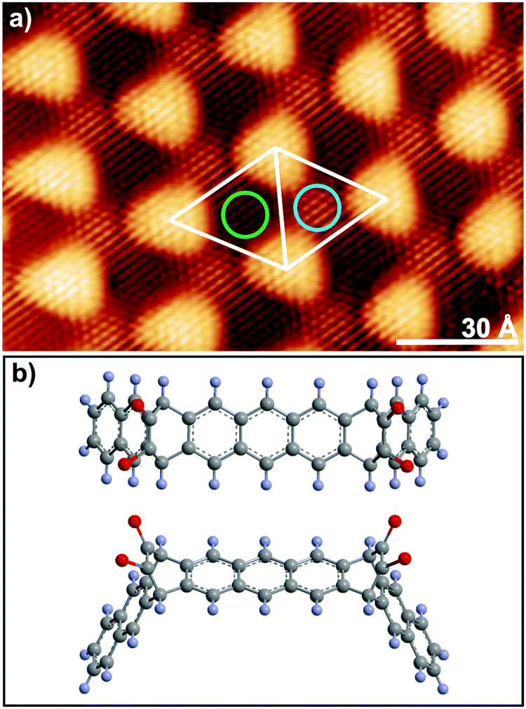 | ||
| Fig. 1 (a) Topographic STM image (13 nm × 8 nm), (Vb = −5 mV, It = 100 pA) of gr/Ru(0001) surface containing several moiré unit cells (white rhombus). The green and blue circles indicate the so-called FCC-Top and HCP-Top areas of the moiré unit cell, respectively. The names indicate the registry with the ruthenium second layer of the three carbon atoms located at threefold hollow sites on the low areas of the moiré.34 (b) Top and perspective views of the structure of the α-bisdiketone nonacene precursors. Carbon and hydrogen atoms are represented in grey and blue, respectively, while the oxygens of each ketone group are represented in red. | ||
A submonolayer coverage of α-bisdiketone nonacene precursors, Fig. 1b, was sublimated under dark conditions on a gr/Ru substrate held at room temperature. The inset in Fig. 2a shows a constant-current STM image of an isolated precursor, exhibiting a rod-like appearance with two bright protrusions of similar apparent height, which we assign to the bridged α-diketone groups pointing upwards. At higher coverages, the intact α-bisdiketone nonacene precursors cover preferentially the low areas of the moiré pattern before populating the upper parts, as shown in Fig. 2a. After deposition of the nonacene precursors, the sample was kept at room temperature and exposed to visible light (λ = 470 nm, φphoton = 2.5 × 1018 cm−2 s−1) for 90 minutes. Upon irradiation, the photodecarbonylation of α-bisdiketone nonacene precursors is achieved which gives rise to the formation of nonacenes. After light exposure the surface is covered with rod-like structures that are randomly distributed over the low areas of the moiré pattern of gr/Ru(0001) and are isolated from each other. Fig. 2b shows an STM image of one of these rod-like structures that is uniform in apparent height. Our DFT calculations (see Materials and methods) confirm that nonacenes are physisorbed on the low areas of the gr/Ru(0001) moiré pattern (see Fig. 2c). The DFT simulated STM image (right panel in Fig. 2b) reproduces the intramolecular resolution in the experimental STM image (left panel in Fig. 2b) and resembles the expected intramolecular resolution of the Lowest Unoccupied Molecular Orbital (LUMO) for a gas phase nonacene (see the ESI†). This indicates that the molecule is electronically decoupled from the substrate.
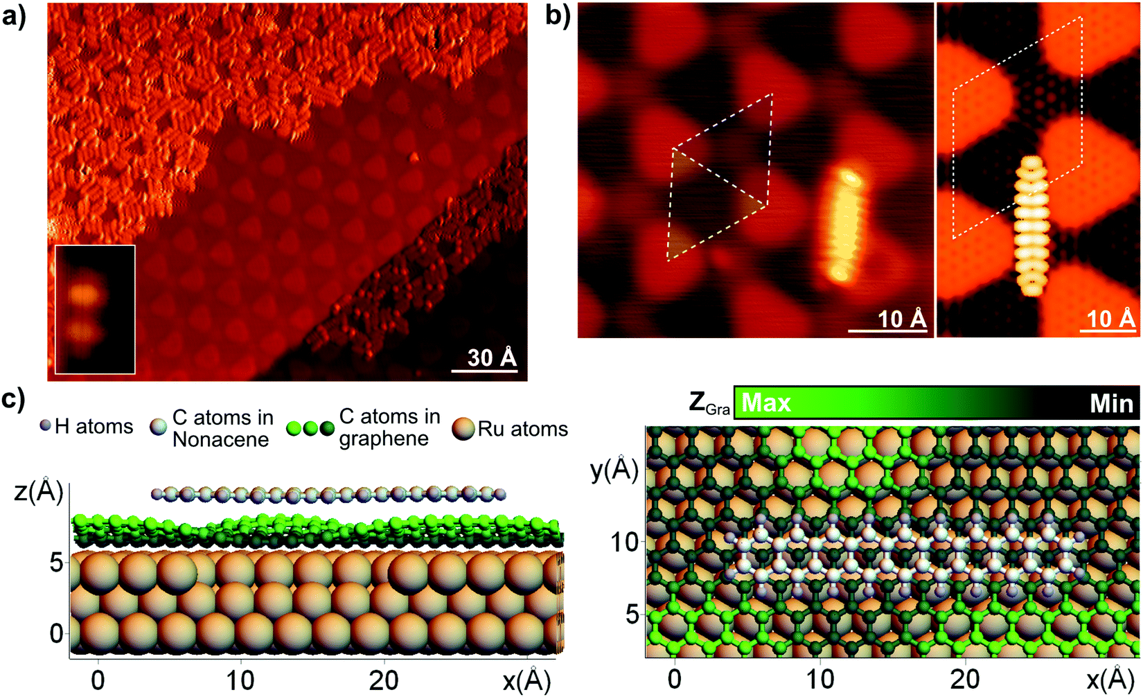 | ||
| Fig. 2 (a) STM topography (Vb = 1.5 V, It = 50 pA) image of α-bisdiketone nonacene precursors on gr/Ru(0001) after room temperature deposition, recorded at 4.6K. The α-bisdiketone nonacene precursors self-assemble by avoiding the ripples of the moiré pattern. Inset shows a topographic image of a single α-bisdiketone nonacene precursor. The two bright protrusions are assigned to the α-diketone groups pointing upwards.30 (b) Left panel: STM image (Vb = 1.7 V, It = 100 pA) of a nonacene molecule adsorbed on the gr/Ru(0001) surface after being exposed to visible light (λ = 470 nm) for 90 minutes. The right panel shows the simulated STM image. (c) DFT calculated geometry showing the most stable physisorbed configuration of a nonacene molecule on gr/Ru(0001). The left panel shows the lateral view and the right panel the top view. Color coding as indicated in the figure legend. | ||
In order to determine the yield of the photogeneration process, we acquired STM images from different areas of the sample after exposure to light. In all the measured images, only nonacenes and no intact precursors were found (see Section II in the ESI† for more details). From these data, we can conclude that a 100% conversion yield was achieved after 90 minutes of exposure to 470 nm light In Table 1, we compare our results with those previously reported on Au(111).30 As can be seen, the on-surface photogeneration of nonacenes is significantly more efficient on gr/Ru(0001) despite the fact that photon fluence and wavelength are the same as in ref. 30, and the latter was carefully chosen to match the n–π* transition of the diketone group and the first optical interband transition of gold37 in order to promote Au(111) electrons into unoccupied orbitals of the precursors via inelastic scattering processes.38,39
| Au(111) | Gr/Ru(0001) | |
|---|---|---|
| Light wavelength | 470 nm | 470 nm |
| Illumination time | 3 hours | 1.5 hours |
| Conversion yield | 80% | 100% |
The crucial factor for the high yield in the conversion is the presence of unoccupied surface states at the gr/Ru(0001) surface, which can host the hot electrons generated by the light adsorption process and facilitate their coupling with the molecular states. The presence of the graphene overlayer induces new states in the projected band gaps of Ru(0001), the so-called image states.40,41 In free-standing graphene, due to the bidimensional nature of the material, image states appear on both sides of the graphene plane.42 When the graphene layer approaches the Ru(0001) surface, the symmetry is broken thus leading to the disappearance of one set of image states. The energy position and the properties of the remaining states depend strongly on the distance between the graphene layer and the ruthenium surface.31 According to state-of-the-art DFT calculations, this distance varies periodically along the moiré pattern, from around 3.4 Å on the ripples (Atop areas in Fig. 1) to 2.2 Å on the lower areas of the moiré (HCP-Top and FCC-Top areas in Fig. 1a).41
Fig. 3a shows an STM image recorded on the gr/Ru sample; for the selected bias voltage, the ripples of the moiré superstructure appear as an ordered triangular array of protrusions. Fig. 3b shows the dZ/dV curves measured on the ripples (blue curve) and the lower areas (red curve) of the moiré. In the curves measured on the ripples, where the distance between graphene and the metallic substrate is large, the first field emission resonance appears around +4.4 eV, close to the average work function measured on this surface.31 The curves measured on the lower areas of the moiré, where the distance between graphene and ruthenium is small, exhibit two peaks in the energy range explored. The peak at +2.85 eV is particularly interesting, because it is due to a surface localized one-electron state: it results from the interaction between the Ru(0001) surface resonance and the lowest image state of graphene.31,44,45 In Fig. 3c we show a dI/dV map measured at +2.85 V, demonstrating that this surface state is uniformly distributed in the low areas of the moiré. Hence, the wave function of this surface state is localized precisely in the region where the nonacene precursors adsorb upon deposition at room temperature. This is a key factor for the on-surface photogeneration of nonacenes on gr/Ru(0001). The energy of this unoccupied surface state matches the energy of the n–π* transition of the diketone group of the α-bisdiketone nonacene precursor, and both the α-bisdiketone nonacene precursors and the surface image state are spatially localized in the low areas of the moiré pattern (see Fig. 2a and 3c). Our results are thus the experimental realization of the scenario theoretically described by Rous,5i.e. a system where the molecular resonance coincides in energy and space with an image state of the substrate.
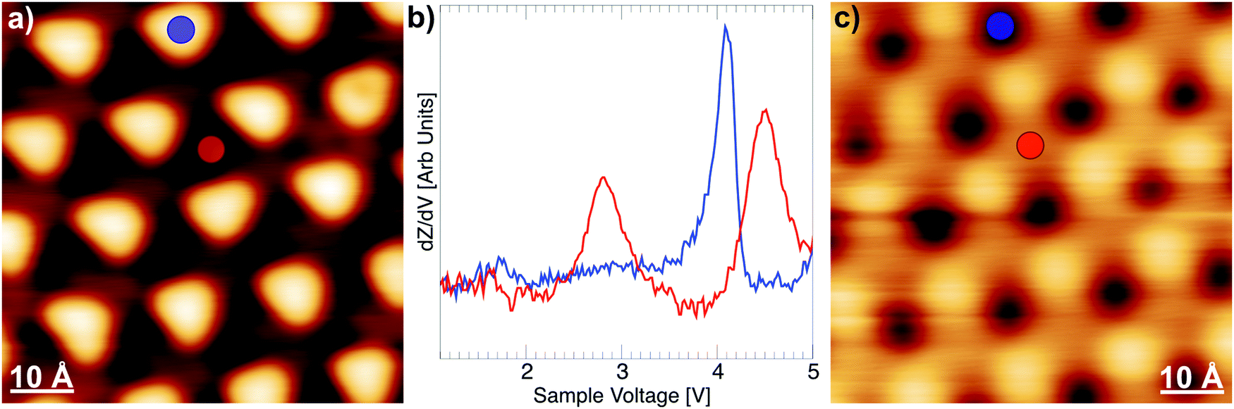 | ||
| Fig. 3 (a) STM topographic image (9 × 9 nm2, Vb = −0,5 V, It = 100 pA) measured at 4.6 K. (b) dZ/dV curves measured on the moiré superstructure reflecting the energy position of the corresponding field emission resonances. The blue curve was acquired on the ripples of the moiré (blue dot in panel a). The red curve was acquired on the low areas of the moiré (red dot in panel a). (c) dZ/dV map measured simultaneously with the image shown in panel a, showing the spatial distribution of the spectral feature appearing in the red spectrum at +2.85 V in the low areas of the moiré. The coloured dots mark the same positions as in panel (a). | ||
Finally, the high conversion efficiency observed in the experiment requires that the gr/Ru(0001) can efficiently absorb photons, thus ensuring the population of the surface states with hot electrons. In order to verify this, we performed Linear Response TD-DFT calculations to retrieve the absorption properties of different materials and surfaces. In Fig. 4 we present the imaginary part of the dielectric function per unit volume of a Ru(0001) surface, freestanding graphene and a Au(111) surface. The low-energy ends of the three spectra are dominated by the so-called Drude peak, which appears due to the conducting nature of the materials. The graphene spectrum, whose intensity is roughly one order of magnitude lower than those of the two metals, is also characterized by a peak at 4 eV, which is the (q → 0) one-body counterpart of the so called π-plasmon (see ESI† for more details), which is typical of graphene and graphitic materials.46–48 The Au(111) spectrum presents a plateau starting at 2 eV, which corresponds to the onset of inter-band transitions from the d bands; we notice that the 470 nm wavelength falls within this plateau. Finally, the Ru(0001) absorption spectrum presents a high absolute value for the 470 nm wavelength and more features than Au(111) due to the presence of empty d bands just above the Fermi level (see also ESI†). The above analysis thus shows that the observed high photogeneration yield on gr/Ru(0001) results from the combination of (i) the high photon absorption on Ru(0001) and (ii) the appearance of a spatially localized surface state at the right energy due to the presence of the graphene adlayer.
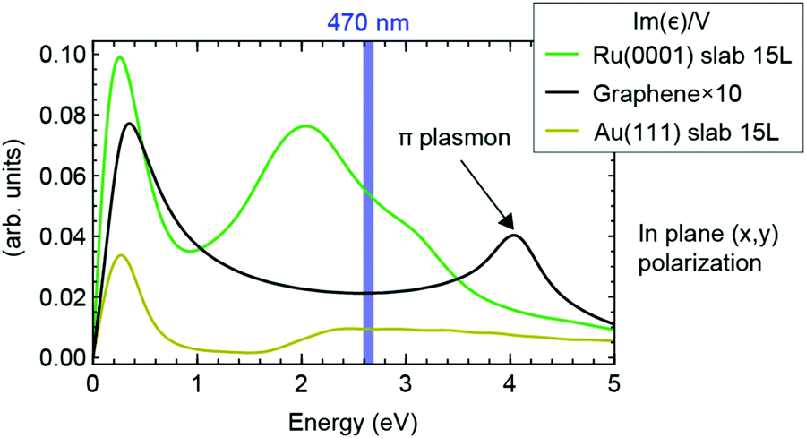 | ||
| Fig. 4 Imaginary part of the dielectric function, ε2(ω) = Im[ε(ω)], per unit volume, representing the optical properties of the three analyzed materials, as obtained in a Linear Response TD-DFT calculation. The graphene results are multiplied by 10 to visualize them on the same scale as those of Au and Ru. The vertical blue gridline marks the energy position of the light used in the experiments. | ||
In summary, we have shown that nonacene formation on gr/Ru(0001) can reach a 100% yield by exposing the corresponding α-bisdiketone precursors to visible light of 470 nm. This represents a gain in light-conversion yield of more than a factor of two with respect to a Au(111) substrate under the same experimental conditions. This higher yield is the consequence of the efficient photon absorption by the ruthenium substrate, the appearance of an unoccupied surface state resonantly coupled to the π* affinity levels of the precursors adsorbed on the low areas of the gr/Ru moiré pattern, and the spatial localization of this surface state in the same moiré regions. These results suggest that surface states can play a prominent role in the surface photochemistry of complex molecular systems by an appropriate selection of a substrate that fulfills the above criteria.
Materials and methods
Sample preparation
The Ru(0001) crystal was Ar+ sputtered, heated in oxygen and flash annealed in vacuum until a (1 × 1) LEED pattern and no traces of contaminants were observed. The graphene samples on Ruthenium were prepared keeping the Ru crystal at 1150 K in UHV and exposed to ethylene at pressures of 2 × 10⁻⁷ mbar for 3 min (48 L, 1 L = 1.33 × 10⁻⁶ mbar s). The temperature was held at 1150K for a further 2 min after removing the C2H4 gas from the chamber. The synthesis of the molecular precursors is described in ref. 30. Molecular precursors were thermally deposited onto a clean gr/Ru(0001) surface held at room temperature. The deposition rate was 0.4 Å min−1 for a sublimation temperature of 610 K. After precursor deposition, the sample was exposed to visible light (Blue (470 nm) LUXEON Rebel LED, mounted on a 40 mm round base with seven LEDs, 490 lm @ 700 mA). During the exposure to light, the sample was kept at room temperature. Subsequently, the sample was introduced in the STM and cooled down to 4.8 K or 1.2 K for inspection. The light source was located outside the STM chamber at approximately 20 cm from the sample and in front of the surface. The estimated photon flux at the sample is 2.5 × 1018 cm−2 s−1.STM experiments
All experiments were performed in a UHV chamber with a base pressure of 5 × 10⁻¹¹ mbar equipped with an LT-STM and facilities for tip and sample preparation. The clean W tips were prepared by Ar+ sputtering (2.5 keV) in UHV for 45 min and then heated up by resistive heating. All the STM/STS data were measured with both tip and sample at 4.8 K or 1.2 K.DFT and TD-DFT calculations
DFT based calculations have been carried out using the PAW method47 (400 eV PW cut-off), as implemented in the VASP package,49–52 using the PBE53 exchange–correlation functional plus the Tkatchenko-Sheffler54 correction, to take into account weak dispersion forces. The graphene ruthenium surface was modelled by a three-layer thick Ru slab oriented in the (0001) direction with a graphene layer adsorbed on one side. To simulate the adsorption of nonacene, we adopted a (22 × 11)graphene/(20 × 10)Ru supercell to minimize the molecule-molecule interactions in the periodic replicas using at least a 20 Å vacuum region in the out of plane direction; notice that the (11 × 11)graphene/(10 × 10)Ru supercell, is capable of reproducing all the physical properties of the graphene ruthenium moiré.43 A full relaxation of the nonacene atoms and of the graphene atoms was carried out until the residual forces on the active atoms were less than 0.01 eV Å−1, limiting the Brillouin Zone integration to the Γ point. The simulated STM images were calculated by the Tersoff Hamann method.55 The images are obtained calculating the isosurfaces of the electron density integrated in the energy window going from the Fermi level to the bias energy, Eb = eVb, where Vb is the bias voltage and e = 1.6 × 10⁻¹⁹C is the elementary charge. The isovalue (Isov) in Å−3 is obtained by the equation Isov = 2 × 10⁻⁴√It in which the tunnelling current (It) value is expressed in nA.The Linear Response TD-DFT calculations were carried out using the PAW based implementation available within the VASP package.56 The ruthenium and gold surfaces were modeled by 15 layer thick slabs (30 Å vacuum region) oriented in the (0001) and (111) directions, respectively, relaxing the coordinates of the outermost layers. The light absorption is calculated as the imaginary part of the dielectric function, ε2(q, ω), normalized to the total volume, in the long wavelength limit (q → 0), and neglecting local field effects. The TD-DFT runs were carried out using unshifted 36 × 36 × 1 k-point mesh (60 × 60 × 1 for graphene). We enforced a very strict 10−8 eV energy tolerance, to ensure precise convergence of the Kohn Sham wave functions, including in the calculation a total of 256, 180, and 60 bands, for the Ru(0001), Au(111), and graphene, respectively, sampling the energy region up to 20 eV above the Fermi level.
Conflicts of interest
There are no conflicts to declare.Acknowledgements
Work partially supported by the Ministerio de Ciencia, Innovación y Universidades projects PGC2018-093291-B-I00, CTQ2017-83531-R, PID2019-105458RB-I00 and PID2019-106732GB-I00 and Comunidad de Madrid projects NMAT2D-CM P20128/NMT-4511 and NanoMagCost. IMDEA Nanoscience acknowledges support from the “Severo Ochoa” Programme for Centres of Excellence in R&D (MINECO, grant SEV-2016-0686). IFIMAC acknowledges support from the “María de Maeztu” Programme for Units of Excellence in R&D (MINECO, grant MDM-2014-0377). Empa acknowledges support by the Swiss National Science Foundation under Grant No. 200020-182015. We acknowledge the allocation of computer time by the Red Española de Supercomputación and the Centro de Computación Científica at the Universidad Autónoma de Madrid (CCC-UAM). NAIST acknowledges support by CREST (JPMJCR15F1) and Grants-in-Aid for Scientific Research (JP20H02816).References
- F. M. Zimmermann and W. Ho, Vibrational excitation dynamics in photodesortption, Surf. Sci. Rep., 1995, 22, 127 CrossRef CAS.
- J. C. Tully, Chemical dynamics at metal surfaces, Annu. Rev. Phys. Chem., 2000, 51, 153 CrossRef CAS.
- C. Frischkorn and M. Wolf, Femtochemistry at metal surfaces: Nonadiabatic reaction dynamics, Chem. Rev., 2006, 106, 4207 CrossRef CAS PubMed.
- C. D. Lindstrom and X.-Y. Zhu, Photoinduced electron transfer at molecule-metal interfaces, Chem. Rev., 2006, 106, 4281–4300 CrossRef CAS PubMed.
- P. J. Rous, Negative ion formation in adsorbed molecules: the role of surface states, Phys. Rev. Lett., 1995, 74, 1835–1838 CrossRef CAS PubMed.
- K. B. K. Tang, P. J. Rous and R. E. Palmer, Energy lifetime of the σ resonance of oriented O2 physisorbed on Ag(110), Phys. Rev. B: Condens. Matter Mater. Phys., 1995, 52, 12395 CrossRef CAS PubMed.
- E. T. Jensen, Charge-transfer photodissociation of adsorbed molecules via electron image states, J. Chem. Phys., 2008, 128, 044301 CrossRef CAS.
- J. E. Anthony, The larger acenes: versatile organic semiconductors, Angew. Chem., Int. Ed., 2008, 47, 452–483 CrossRef CAS PubMed.
- J. E. Anthony, Functionalized acenes and heteroacenes for organic electronics, Chem. Rev., 2006, 106, 5028–5048 CrossRef CAS PubMed.
- Z. Sun, Q. Ye, C. Chi and J. Wu, Low band gap polycyclic hydrocarbons: from closed-shell near infrared dyes and semiconductors to open-shell radicals, Chem. Soc. Rev., 2012, 41, 7857–7889 RSC.
- M. Watanabe, et al., The synthesis, crystal structure and chargetransport properties of hexacene, Nat. Chem., 2012, 4, 574–578 CrossRef CAS PubMed.
- M. Fujita, K. Wakabayashi, K. Nakada and K. Kusakabe, Peculiar localized state at zigzag graphite edge, J. Phys. Soc. Jpn., 1996, 65, 1920–1923 CrossRef CAS.
- P. Ruffieux, et al., On-surface synthesis of graphene nanoribbons with zigzag edge topology, Nature, 2016, 531, 489–492 CrossRef CAS PubMed.
- D. Biermann and W. Schmidt, Diels-Alder reactivity of polycyclic aromatic hydrocarbons. Acenes and benzologs, J. Am. Chem. Soc., 1980, 102, 3163–3173 CrossRef CAS.
- A. R. Reddy, G. Fridman-Marueli and M. Bendikov, Kinetic and thermodynamic stability of acenes: theoretical study of nucleophilic and electrophilic addition, J. Org. Chem., 2007, 72, 51–61 CrossRef CAS PubMed.
- P. von Schleyer, R. Manoharan, H. Jiao and F. Stahl, The acenes: is there a relationship between aromatic stabilization and reactivity?, Org. Lett., 2001, 3, 3643–3646 CrossRef PubMed.
- R. Mondal, R. M. Adhikari, B. K. Shah and D. C. Neckers, Revisiting the stability of hexacenes, Org. Lett., 2007, 9, 2505–2508 CrossRef CAS PubMed.
- R. Mondal, B. Shah and D. C. Neckers, Photogeneration of heptacene in a polymer matrix, J. Am. Chem. Soc., 2006, 128, 9612–9613 CrossRef CAS PubMed.
- C. Tönshoff and H. F. Bettinger, Photogeneration of octacene and nonacene, Angew. Chem., Int. Ed., 2010, 49, 4125–4128 CrossRef PubMed.
- R. Dorel and A. M. Echavarren, Strategies for the synthesis of higher acenes, Eur. J. Org. Chem., 2017, 14–24 CrossRef CAS PubMed.
- H. F. Bettinger and C. Tönshoff, The longest acenes, Chem. Rec., 2015, 15, 364–369 CrossRef CAS PubMed.
- M. Watanabe, et al., The synthesis, crystal structure and charge-transport properties of hexacene, Nat. Chem., 2021, 4, 574–578 CrossRef PubMed.
- J. I. Urgel, et al., On-surface synthesis of heptacene organometallic complexes, J. Am. Chem. Soc., 2017, 139, 11658–11661 CrossRef CAS PubMed.
- M. Zugermeier, et al., On-surface synthesis of heptacene and its interaction with a metal surface, Nanoscale, 2017, 9, 12461 RSC.
- R. Zuzak, et al., Nonacene generated by on-surface dehydrogenation, ACS Nano, 2017, 11, 9321–9329 CrossRef CAS PubMed.
- L. Colazzo, et al., On-surface synthesis of heptacene on Ag (001) from brominated and non-brominated tetrahydroheptacene precursors, Chem. Commun., 2018, 54, 10260–10263 RSC.
- R. Zuzak, et al., Higher Acenes by On-Surface Dehydrogenation: From Heptacene to Undecacene, Angew. Chem., Int. Ed., 2018, 57, 10500–10505 CrossRef CAS PubMed.
- J. Krüger, et al., Decacene: On-Surface Generation, Angew. Chem., 2017, 129, 12107–12110 CrossRef.
- F. Eisenhut, et al., Dodecacene generated on surface: reopening of the energy gap, ACS Nano, 2019, 14, 1011–1017 CrossRef PubMed.
- J. I. Urgel, et al., On-surface light-induced generation of higher acenes and elucidation of their open-shell character, Nat. Commun., 2019, 10, 861 CrossRef PubMed.
- B. Borca, S. Barja, M. Garnica, D. Sánchez-Portal, V. M. Silkin, E. V. Chulkov, C. F. Hermanns, J. J. Hinarejos, A. L. Vázquez de Parga, A. Arnau, P. M. Echenique and R. Miranda, Potential Energy Landscape for Hot Electrons in Periodically Nanostructured Graphene, Phys. Rev. Lett., 2010, 105, 036804 CrossRef CAS.
- N. Ambrust, J. Güdde. P. Jakob, U. Höfer, Time resolved two photon photoemission of unoccupied electronic states of periodically rippled graphene on Ru(0001), Phys. Rev. Lett., 2012, 108, 056801 CrossRef PubMed.
- S. Marchini, S. Günther and J. Wintterlin, Scanning tunneling microscopy of graphene on Ru(0001), Phys. Rev. B: Condens. Matter Mater. Phys., 2007, 76, 075429 CrossRef.
- A. L. Vázquez de Parga, F. Calleja, B. Borca, M. C. G. Passeggi Jr., J. J. Hinarejos, F. Guinea and R. Miranda, Periodically rippled graphene: Growth and spatially resolved electronic structure, Phys. Rev. Lett., 2008, 100, 056807 CrossRef PubMed.
- A. B. Preobrajenski, M. L. Ng, S. Vinogradov and N. Martensson, Controlling Graphene corrugation on lattice-mismatched substrates, Phys. Rev. B: Condens. Matter Mater. Phys., 2008, 78, 073401 CrossRef.
- B. Borca, S. Barja, M. Garnica, M. Minniti, A. Politano, J. M. Rodriguez-García, J. J. Hinarejos, D. Farías, A. L. Vázquez de Parga and R. Miranda, Electronic and geometric corrugation of periodically rippled, self-nanostructured graphene epitaxially grown on Ru(0001), New J. Phys., 2010, 12, 093018 CrossRef.
- P. B. Johnson and R. W. Christy, Optical constants of the noble metals, Phys. Rev. B: Solid State, 1972, 6, 4370–4379 CrossRef CAS.
- C. Frischkorn and M. Wolf, Femtochemistry at metal surfaces: Nonadiabatic reaction dynamics, Chem. Rev., 2006, 106, 4207 CrossRef CAS PubMed.
- C. D. Lindstrom and X.-Y. Zhu, Photoinduced electron transfer at molecule-metal interfaces, Chem. Rev., 2006, 106, 4281–4300 CrossRef CAS PubMed.
- P. M. Echenique and J. B. Pendry, The existence and detection of Rydberg states at surfaces, J. Phys. C: Solid State Phys., 1978, 11, 2065 CrossRef CAS.
- F. J. Himpsel, K. Christman, P. Heimann, D. E. Eastman and P. J. Feibelman, Adsorbate band dispersion for C on Ru(001), Surf. Sci., 1982, 115, L159 CrossRef CAS.
- V. M. Silkin, J. Zhao, F. Guinea, E. V. Chulkov, P. M. Echenique and H. Petek, Image potential states in graphene, Phys. Rev. B: Condens. Matter Mater. Phys., 2009, 80, 121408R CrossRef.
- D. Stradi, S. Barja, C. Díaz, M. Garnica, B. Borca, J. J. Hinarejos, D. Sánchez-Portal, M. Alcamí, A. Arnau, A. L. Vázquez de Parga, R. Miranda and F. Martín, Role of the dipersion forces in the structure of graphene monolayers on Ru surfaces, Phys. Rev. Lett., 2011, 106, 186102 CrossRef CAS PubMed.
- N. Ambrust, J. Güdde, P. Jakob and U. Höfer, Time-resolved two-photon photoemission of unoccupied electronic states of periodically rippled graphene on Ru(0001), Phys. Rev. Lett., 2021, 108, 056801 CrossRef PubMed.
- V. del Campo, J. D. Correa, J. Correa-Puerta, D. Kroeger and P. Häberle, Unoccupied electronic states of Ru(0002), Surf. Sci., 2016, 653, 163 CrossRef CAS.
- V. Despoja, D. Novko, K. Dekanić, M. Šunjić and L. Marušić, Two-dimensional and pi-plasmon spectra in pristine and doped graphene, Phys. Rev. B: Condens. Matter Mater. Phys., 2013, 87, 075447 CrossRef.
- M. Pisarra, A. Sindona, M. Gravina, V. M. Silkin and J. M. Pitarke, Dielectric screening and plasmon resonances in bilayer graphene, Phys. Rev. B, 2016, 93, 035440 CrossRef.
- C. Vacacela Gomez, M. Pisarra, M. Gravina, P. Riccardi and A. Sindona, Plasmon properties and hybridization effects in silicene, Phys. Rev. B, 2017, 95, 085419 CrossRef.
- P. E. Blochl, Projector Augmented-Wave Method, Phys. Rev. B: Condens. Matter Mater. Phys., 1994, 50, 17953 CrossRef PubMed.
- G. Kresse and D. Joubert, From ultrasoft pseudopotentials to the projector augmented-wave method, Phys. Rev. B: Condens. Matter Mater. Phys., 1999, 59, 1758 CrossRef CAS.
- G. Kresse and J. Furthmuller, Efficiency of ab-initio total energy calculations for metals and semiconductors using a plane-wave basis set, Comput. Mater. Sci., 1996, 6, 15 CrossRef CAS.
- G. Kresse and J. Furthmuller, Efficient iterative schemes for ab initio total-energy calculations using a plane-wave basis set, Phys. Rev. B: Condens. Matter Mater. Phys., 1996, 54, 11169 CrossRef CAS PubMed.
- J. P. Perdew, K. Burke and M. Ernzerhof, Generalized Gradient Approximation Made Simple, Phys. Rev. Lett., 1996, 77, 3865 CrossRef CAS PubMed.
- A. Tkatchenko and M. Scheffler, Accurate Molecular van der Waals Interactions from Ground-State Electron Density and Free-Atom Reference Data, Phys. Rev. Lett., 2009, 102, 073005 CrossRef PubMed.
- J. Tersoff and D. R. Hamman, Theory and application for the scanning tunneling microscope, Phys. Rev. Lett., 1983, 50, 1998–2001 CrossRef CAS.
- M. Gajdos, K. Hummer, G. Kresse, J. Furthmuller and F. Bechstedt, Linear optical properties in the projector-augmented wave method, Phys. Rev. B: Condens. Matter Mater. Phys., 2006, 73, 045112 CrossRef.
Footnotes |
| † Electronic supplementary information (ESI) available. See DOI: 10.1039/d1nh00184a |
| ‡ Authors contribute equally to this work. |
| § Present address: Department of Interface Science, Fritz-Haber Institute of the Max-Planck Society, 14195 Berlin, Germany. |
| ¶ Present address: Departamento de Química Física, Facultad de C.C. Químicas, Universidad complutense de Madrid, 28040 Madrid, Spain. |
| This journal is © The Royal Society of Chemistry 2021 |