
Understanding the role of facets and twin defects in the optical performance of GaAs nanowires for laser applications†
Zahra
Azimi
 *a,
Nikita
Gagrani
a,
Jiangtao
Qu
b,
Olivier L. C.
Lem
c,
Sudha
Mokkapati
d,
Julie M.
Cairney
b,
Rongkun
Zheng
e,
Hark Hoe
Tan
af,
Chennupati
Jagadish
af and
Jennifer
Wong-Leung
*a
*a,
Nikita
Gagrani
a,
Jiangtao
Qu
b,
Olivier L. C.
Lem
c,
Sudha
Mokkapati
d,
Julie M.
Cairney
b,
Rongkun
Zheng
e,
Hark Hoe
Tan
af,
Chennupati
Jagadish
af and
Jennifer
Wong-Leung
*a
aDepartment of Electronic Materials Engineering, Research School of Physics, The Australian National University, Canberra, Australia. E-mail: zahra.azimi@anu.edu.au; jenny.wongleung@anu.edu.au
bAerospace, Mechanical and Mechatronic Engineering, The University of Sydney, Sydney, NSW 2006, Australia
cAustralian National Fabrication Facility ACT Node, Research School of Physics, The Australian National University, Canberra, ACT 2601, Australia
dDepartment of Materials Science and Engineering, Faculty of Engineering, Monash University, Clayton, VIC 3800, Australia
eThe School of Physics, The University of Sydney, Sydney, NSW 2006, Australia
fAustralian Research Council Centre of Excellence for Transformative Meta-Optical Systems, Research School of Physics, The Australian National University, Canberra, ACT 2601, Australia
First published on 6th May 2021
Abstract
GaAs nanowires are regarded as promising building blocks of future optoelectronic devices. Despite progress, the growth of high optical quality GaAs nanowires is a standing challenge. Understanding the role of twin defects and nanowire facets on the optical emission and minority carrier lifetime of GaAs nanowires is key for the engineering of their optoelectronic properties. Here, we present new insights into the microstructural parameters controlling the optical properties of GaAs nanowires, grown via selective-area metal–organic vapor-phase epitaxy. We observe that these GaAs nanowires have a twinned zinc blende crystal structure with taper-free {110} side facets that result in an ultra-low surface recombination velocity of 3.5 × 104 cm s−1. This is an order of magnitude lower than that reported for defect-free GaAs nanowires grown by the vapor–liquid–solid technique. Using time-resolved photoluminescence and cathodoluminescence measurements, we untangle the local correlation between structural and optical properties demonstrating the superior role of the side facets in determining recombination rates over that played by twin defects. The low surface recombination velocity of these taper-free {110} side facets enable us to demonstrate, for the first time, low-temperature lasing from bare (unpassivated) GaAs nanowires, and also efficient room-temperature lasing after passivation with an AlGaAs shell.
New conceptsIn this work, we elucidate a new concept of engineering high optical quality in GaAs nanowires by facet engineering. GaAs nanowires have promising applications for optoelectronic array devices but the growth of defect-free GaAs nanowires by selected area metal organic vapour phase epitaxy is a longstanding challenge. We report on the optical properties of high quality zinc blende GaAs nanowires grown by this technique. By correlating the local concentration of defects to the optical emission efficiency along the nanowire, we conclusively show that catalyst-free GaAs nanowires with {110} side facets have the lowest surface recombination velocity reported for GaAs nanowires, despite the presence of twin defects. We demonstrate the first low-temperature lasing of unpassivated GaAs nanowires, achievable because of their superior optical properties. By passivating these nanowires with an AlGaAs shell, we further achieve efficient room temperature lasing. These insights provide new directions for the scalable fabrication and integration of GaAs nanowires in efficient optoelectronic devices with applications ranging from light-harvesting to telecommunication and light-emitting devices. |
Introduction
The possibility of designing complex GaAs nanowire crystal structures, not feasible in the bulk material has attracted significant interest for engineering future optoelectronic devices.1–3 Formation of crystal imperfections such as stacking faults, twin defects and wurtzite/zinc blende (WZ/ZB) heterostructures within a single nanowire is common during nanowire growth.4–7 These imperfections modify the band structure and form some mini-bands or type II band alignment that largely determine the optoelectronic properties of the nanowire.5,6,8 For example, the formation of periodic twins along the growth axis of the InP nanowire has been used as superlattice structures,4 resulting in a shift of the emission peaks, due to the confinement of the carriers at the twin planes.9 In contrast, the presence of randomly spaced twin planes and WZ/ZB heterostructures along the nanowire has been reported to adversely affect coherent electron transport.1,10,11 The lower carrier mobility, lifetime and quantum efficiency of these imperfect nanowire crystal structures limit their optoelectronic performance and potential use in devices.10,11Perfect ZB and WZ GaAs nanowire structures and superlattice structures have been obtained using Au nanoparticles as a catalyst in vapor–liquid–solid (VLS) growth.7,12,13 However, GaAs nanowires grown via the VLS method have some limitations, namely defect formation in large diameter nanowires,1 tapering as a result of the simultaneous radial growth, incorporation of carbon impurities on the sidewalls14 and Au incorporation inside the nanowires.15 These problems have deleterious effects on the nanowire optoelectronic properties and can be virtually eliminated in nanowires grown in metal catalyst-free conditions, where taper-free nanowires are formed with uniform side facets16–19 and no foreign impurities. The ability to form nanowire arrays via selective-area epitaxy (SAE) makes them ideal for applications requiring a specific arrangement of nanowires like transistors,20 solar cells,21 and photonic and plasmonic devices.22,23 Therefore, catalyst-free SAE grown nanowires are ideal for optoelectronic devices. However, controlling the crystal structure and achieving perfect crystal quality GaAs nanowires with this method is still a challenge.18,19,24 Usually, catalyst free growth of GaAs nanowires leads to the formation of predominantly ZB crystal structures with some small fractions of WZ defects.18,19 The WZ structure is not energetically favourable in bulk III-As and III-P semiconductors, due to relatively low electronegativity difference between the group III and (P, As) elements.25 The WZ structure has a lower surface energy than ZB and thus it is increasingly favorable in nanowires with smaller diameters.26,27 However, GaAs has amongst the lowest ionic characteristic of III-As and III-P semiconductors.
Apart from the microstructural challenge, GaAs has a high surface recombination velocity of ∼106 cm s−1.28–30 This is especially detrimental in nanowires because of their high surface area-to-volume ratio. For GaAs nanowires with diameters below 500 nm and low doping concentrations (<1016 cm−3), this high surface recombination velocity may result in a complete carrier depletion.24 Passivation of the GaAs nanowire sidewalls can be achieved by growing an optimized AlGaAs shell to minimize surface recombination.31,32 The passivated GaAs nanowires exhibit increased minority-carrier lifetime (τmc) and electron mobilities.32–34 With an AlGaAs passivation shell, several groups35–37 have reported optically pumped lasing in GaAs/AlGaAs core/shell nanowires. Room temperature lasing has been also demonstrated in defect-free passivated nanowires.35
Here, we demonstrate that GaAs nanowires, grown by selective-area metal–organic vapour-phase epitaxy (SA-MOVPE), have superior optical properties with an ultra-low surface recombination velocity of 3.5 × 104 cm s−1 compared to GaAs nanowires grown by VLS.28,31,38 We show a direct correlation between the local crystal structure and optical properties by comparing the transmission electron microscopy (TEM) analysis with time-resolved photoluminescence (TRPL) and cathodoluminescence (CL) along the nanowire. Notably, we demonstrate the first reported low-temperature lasing in GaAs nanowires without the need of surface passivation because of the ultra-low surface recombination velocity of their taper-free {110} surfaces. We also demonstrate room-temperature lasing with a very low lasing threshold upon surface passivation.
Results and discussion
Fig. 1a and b show SEM images of the GaAs nanowires grown under the optimized conditions (see Section 1 of the ESI†). Uniform GaAs nanowires were grown vertically with an average length of 7 μm and a diameter of 460 nm (Fig. 1a and b). The top view SEM image shows a uniform hexagonal nanowire cross-section with {110} side facets, while the nanowire tips have a variety of morphologies. About 55% of the nanowires have a flat tip with a pure (111)B facet (Fig. 1a, red circle), while 37% have tips made of three inclined {110} facets intersecting the (111)B top facet (Fig. 1a, blue circle). The remaining nanowires have irregular tips, composed of a combination of inclined facets in addition to the (111)B and {110} facets (Fig. 1a, yellow circle). The nanowire tip morphology provides an insight into the nanowire growth and twin defect formation mechanism.19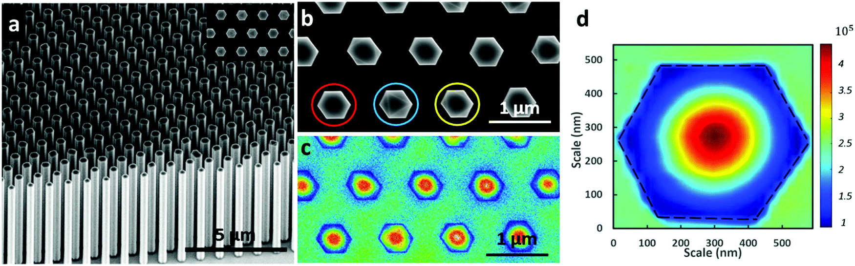 | ||
| Fig. 1 (a) 45° tilt view SEM image of the GaAs nanowires grown under the optimised growth conditions. Inset shows the corresponding top view SEM from the middle of the array. (b) Top view SEM and (c) corresponding panchromatic CL images of the nanowire array. (d) Panchromatic CL image extracted from the spectral map of the nanowire highlighted by the red circle in (b). | ||
The optical properties of the nanowire tips were investigated by cathodoluminescence (CL) measurements at room temperature. Regardless of the tip morphology, a sharp emission peak at 870 nm was observed for all nanowires (Fig. 1c). Fig. 1d shows a top view CL intensity map (CL mapping step size is 20 nm) of a nanowire with a pure (111)B tip facet. A strong luminescence intensity, peaking in the middle of the nanowire is observed with radially decreasing intensity towards the nanowire edges. This is attributed to surface recombination at the nanowire surface. The spontaneous oxidation of the nanowire surface generates surface states that act as non-radiative recombination centres for free carriers,31 resulting in a high surface recombination velocity of 5.4 × 105 cm s−1 for GaAs nanowires grown by VLS,28 which may result in a complete carrier depletion for nanowires with diameters below 500 nm.24 However, the panchromatic CL intensity map in Fig. 1d shows that the depletion region within the nanowire is a cylindrical shell, with the CL intensity 4 to 5 times smaller at the edge of the nanowire compared to the centre.
To assess the nanowire optical properties and crystal structure, CL and TEM were carried out along the length of the GaAs nanowire. TEM analysis reveals a series of twin ZB segments along the length of the nanowire (Fig. 2). Fig. 2c shows a representative selected area diffraction pattern of a nanowire section. The diffraction spots can be separated into two sets of reflections attributed to the two individual ZB twin variants. The ZB twins have a (111) twin boundary and 180° rotation around the 〈111〉 axis perpendicular to the twin boundary. For ease of understanding, the diffraction spots associated with each ZB twin are labelled as red and blue. Fig. 2b shows a montage of individual dark field TEM images obtained along the length of the nanowire using the  twin reflection highlighted in Fig. 2b to form the image. Specifically, only one twin variant is selected for the dark field and consequently appears bright such that the individual ZB twins appear as alternate dark and light regions. Similarly, the individual twin variants are clearly visible in the high-resolution aberration-corrected transmission electron microscopy (AC-TEM) images. Fig. 2e and f are typical high resolution TEM images taken within 0.5 μm from the base and the top of a nanowire, respectively. Since the nanowires were physically broken off the substrate with a glass needle, the bottom ends were not flat (Fig. S5, ESI†). The boundaries between individual twins are twin planes/defects and an atomic model of the twin boundary is illustrated in Fig. 2d. Notably, Fig. 2b shows that the twin plane density is not uniform along the nanowire longitudinal axis. The base of the GaAs nanowire has a significantly higher twin defect density compared to regions closer to its tip. In particular, the twin defect density, ntdd decreases from 110 μm−1 near the base to 13 μm−1 near the top.
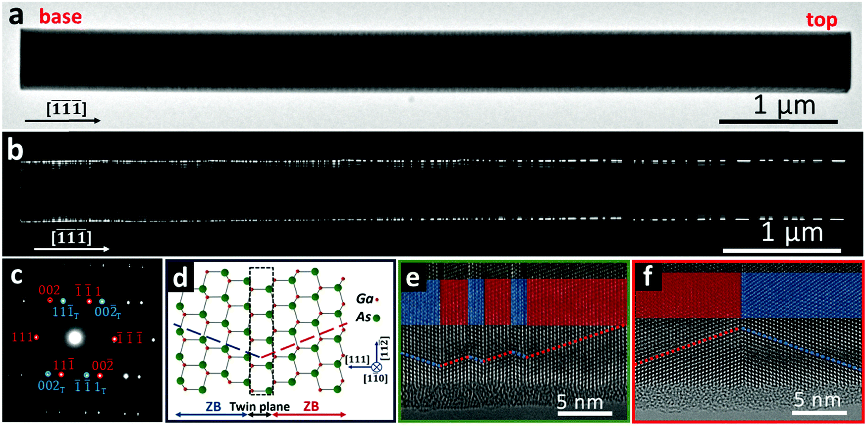 | ||
Fig. 2 TEM results of a GaAs nanowire. (a) Bright-field TEM image of the nanowire, (b) dark-field TEM image of the same nanowire, and (c) selected area diffraction pattern of the nanowire. The different colours are assigned to the two twin variants of the zinc blende structure. (d) Illustration of the atomic structure of a twin defect. (e) Typical high-resolution AC-TEM images from (e) the bottom and (f) the top region of the nanowire. All TEM images and diffraction patterns were taken along the [1![[1 with combining macron]](https://www.rsc.org/images/entities/char_0031_0304.gif) 0] zone axis. 0] zone axis. | ||
In order to evaluate the uniformity of the nanowire optical properties, CL emission was collected along the length of the nanowire at room temperature. Fig. 3a shows the CL intensity map and the profile along the nanowire, together with an SEM image of the nanowire. The CL intensity increases by over an order of magnitude from the base to the top of the nanowire, while the CL peak position (Fig. 3b) is blue-shifted from the base (897 nm) to the top (886 nm). Axial variation of the GaAs nanowire luminescence emission has been attributed to various factors such as variation in diameter,31 doping concentrations,38,39 and structural polytype phases.40–43 Variations in the diameter and composition can be excluded given the uniform diameter of the GaAs nanowires along their length. In order to understand the variation in the CL emission along the nanowire and local twin defect density, correlated TEM and CL were carried out on six nanowires and the results were consistent. We observed a red shift in the CL peak position and a reduction in CL intensity with increasing twin defect density. A red shift in the PL emission has been observed in mixed phase GaAs nanowires with increasing proportion of wurtzite (WZ) segments.6,10 Yet our nanowire structure has only unit layers of wurtzite (isolated twin defects), with decreasing density from the bottom to the top of the nanowire.
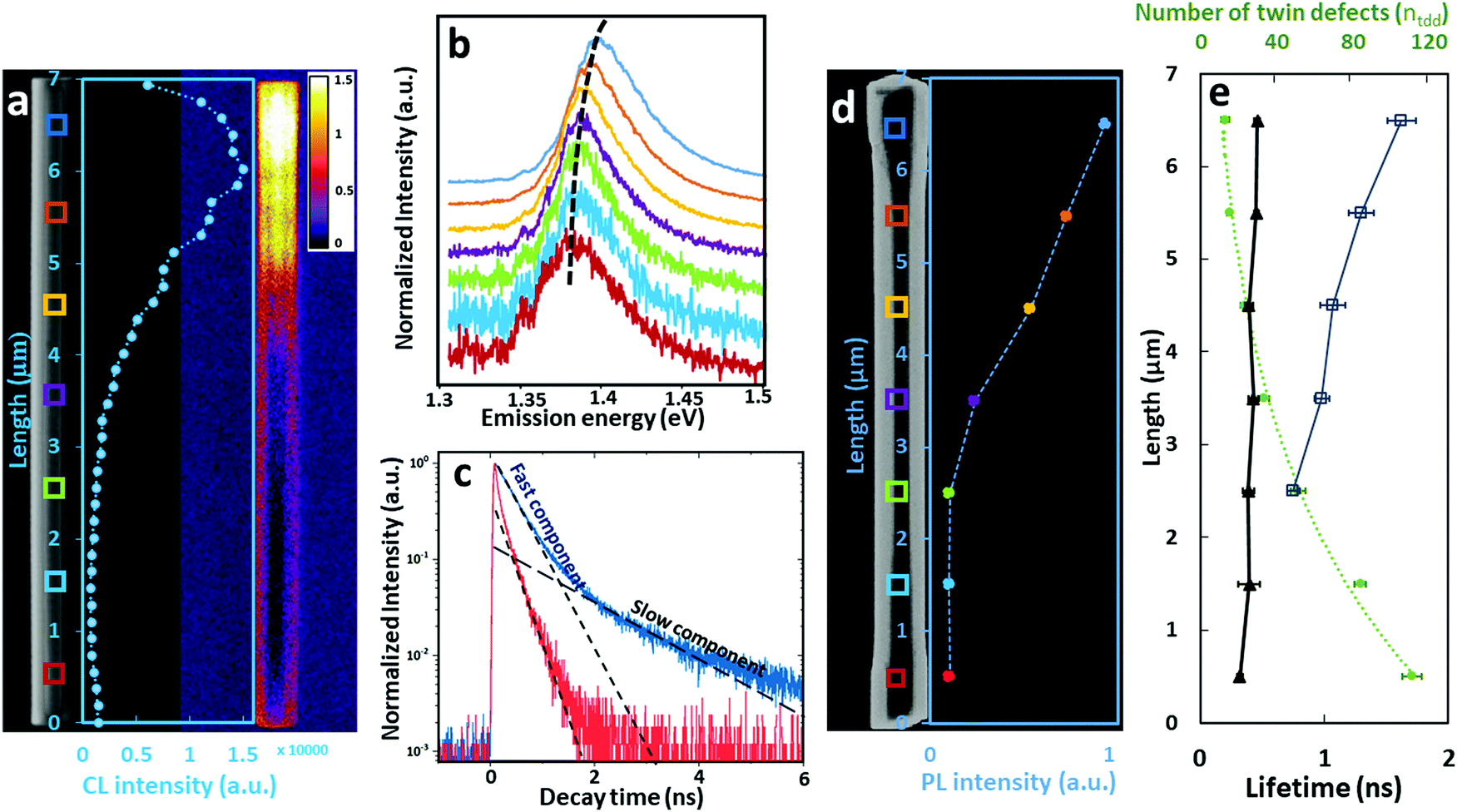 | ||
| Fig. 3 Room temperature CL and PL results from GaAs and GaAs/AlGaAs core/shell nanowires, respectively. (a) SEM and CL intensities along a GaAs nanowire, and panchromatic CL image of the same nanowire. (b) CL spectra from the 7 coloured boxes in (a). (c) Time-resolved PL from the base (red) and top (blue) of the GaAs/AlGaAs core/shell nanowire. (d) SEM of a GaAs/AlGaAs core/shell nanowire and relative PL intensities in different regions of the nanowire as indicated by coloured boxes. (e) Plot showing the variation in the primary (black triangles) and secondary (black opened squares) carrier lifetimes, and twin defect density (green) along the length of the GaAs/AlGaAs nanowire. | ||
To understand the mechanisms driving the observed red shift and the change of CL intensity, low temperature (80 K) CL was performed along the nanowire length1 (see Section 3.1 of the ESI†). We observed that the CL intensity decreases with increasing twin defect density (ntdd), moving toward the nanowire base. This suggests that twin defects act as non-radiative recombination sites, trapping the charge carriers. Furthermore, with increasing twin defect density from the top to the base (Fig. 2b), the CL emission is red shifted by 10 meV (Fig. S6, ESI†). This red shift can be assigned to more recombination of electron–holes at twin plane sites. This suggests that twin defects act as type II band alignment sites with radiative recombination at a lower energy than the main exciton energy level as well as non-radiative recombination. Low temperature (8 K) power-dependent PL measurement further supports the formation of type II band alignment at twin defects (Section 3.2 of the ESI†).
In order to understand their optical properties further, both micro-PL and TRPL were collected from the middle of the nanowires. Irrespective of the nanowire diameter, their TRPL time decay curves reveal a single exponential decay. The minority carrier lifetimes were extracted by fitting the data. By comparing the TRPL results for nanowires with different diameters, a surface recombination velocity (SRV) of 3.5 × 104 cm s−1 was calculated for our SAE GaAs nanowires (see Section 4.4 of the ESI†). This is an order of magnitude lower than the SRV reported for ZB GaAs grown by VLS with both Au and Ga catalysts28,31 and two orders of magnitude lower compared to Zn+ doped GaAs nanowires.38
The sidewalls of GaAs nanowires grown by Au catalysts consist of a mixture of {112}A and {112}B planes,44 while the sidewalls of Zn+ doped GaAs nanowires consist of {111}A and {111}B planes.7 We attribute the low surface recombination of these catalyst-free SAE-grown GaAs nanowires to their taper-free {110} facets, which have also been proposed to have lower surface recombination velocity.45 The strong luminescence intensity, peaking in the middle of the cross section (Fig. 1d), and the low SRV (3.5 × 104 cm s−1) of our catalyst-free SAE-grown nanowires are a direct result of the low surface recombination of the taper-free {110} side facets.
We also investigated our GaAs nanowires which were passivated with an AlGaAs shell to further minimize surface recombination. A GaAs cap layer was then grown after the AlGaAs shell to prevent oxidation. By analyzing the micro-PL and TRPL spectra at different spots on single passivated nanowires, we are able to gain insight into the local variation of the optical properties along the length of the nanowire. The intensity of the micro-PL peak at 7 different spots along the nanowire is plotted in Fig. 3d. Position dependent optical emissions were also observed in SAE-grown GaAs/AlGaAs core/shell nanowires by Chang et al. and attributed to a decrease in the thickness of the AlGaAs shell towards the base of the nanowire.24 Here, given the uniformity of the AlGaAs shell, the local variations are related to the GaAs core. The variation in the PL peak intensity (Fig. 3d) is consistent with the variation in the CL intensity (Fig. 3a), described earlier, with the highest PL intensity observed at the top of the nanowire, where the twin defect density is the lowest. Fig. 3e (green line) shows the average local twin plane density (ntdd), extracted from Fig. 2b for 1 μm sections along the length of the nanowire. The TRPL data collected at different spots along the nanowire show a direct correlation with the twin defect density. Within the first 2 μm from the base of the nanowire, the twin defect density is greater than 60 μm−1 and the TRPL data showed a single exponential decay with a carrier lifetime of 0.36 ± 0.05 ns (Fig. 3c, red curve). However, within the rest of the nanowire, the TRPL data show two exponential decays, a fast and slow component (Fig. 3c, blue curve). Thus, a primary and secondary carrier lifetime can be extracted from fitting the fast and slow decay components, respectively. Chang et al. also reported a bi-exponential decay with two lifetimes of 0.2 and 1.3 ns in SAE-grown GaAs/AlGaAs core/shell nanowires.24 However, these two lifetimes were not associated with specific recombination mechanisms. Fig. 3e correlates the primary and secondary carrier lifetimes with the twin density at different positions along the nanowire. The primary carrier lifetime (Fig. 3e, black triangles) is fairly constant along the nanowire with an average value of 0.43 ± 0.026 ns, whereas the secondary carrier lifetime (Fig. 3e, opened grey squares) increases from 0.75 to 1.62 ns towards the top of the nanowire. The primary carrier lifetime is well above the response of the optical system, which is around 80 ps.38 The presence of these two time-decays indicates the contribution of at least two deep level defect types.46 These two defect types are the recombination sites at the GaAs/AlGaAs interface and twin defects.47,48 The constant primary lifetime is attributed to recombination at the GaAs/AlGaAs interface (τS) as this component should not vary significantly along the nanowire, considering its uniform diameter and sidewalls (Fig. 3a and d). We note that the primary lifetime trends down slightly at the base of the nanowire. This is tentatively attributed to the higher twin defect density at the base of the nanowire, which can result in zigzag nanofacets on the {110} sidewalls (Fig. 2e).
The secondary lifetime is attributed to recombination at twin defect sites (τTDS). For twin defect densities below 60 μm−1, there is an inverse power law relationship between the secondary carrier lifetime component (shown with opened squares) and the twin defect density (green) as shown in Fig. 3e. More information about the carrier lifetime and the relationship between τTDS and ntdd can be found in Section 4 of the ESI.† The longer twin-free ZB segments lead to longer recombination lifetimes, due to the lower density of recombination sites. For twin defect densities above 60 μm−1, the secondary carrier lifetime becomes comparable to the constant primary carrier lifetime, thus explaining the single exponential decay observed at the base of the nanowire. The detrimental effect of twins on SRV has been demonstrated previously.49 Here we discern the individual contribution of facets and twin defect density on the resulting surface recombination velocity. Our key finding is that the GaAs nanowires grown under optimized growth conditions with taper-free {110} facets resulted in an ultralow recombination velocity despite the presence of the twin defects.
We estimate an SRV of ∼1.65 × 104 cm s−1 for the passivated GaAs (see ESI†, SRV at GaAs/AlGaAs interface). It should be mentioned that the AlGaAs shell thickness and quality were not optimized in our GaAs/AlGaAs core/shell, and thus the SRV could be further improved. Previous reports have shown that two orders of magnitude reduction in surface recombination velocity of GaAs nanowires can be achieved by optimizing the AlGaAs passivation shell.31,32
The quantum efficiency (QE) of the nanowires represents their optical quality and can be estimated by ηi = τnr/(τnr + τr), where τnr and τr are the non-radiative and radiative lifetimes, respectively.45 At room temperature and with a low pump fluence of 1 μJ cm−2 per pulse, the non-radiative lifetime of 0.23 ± 0.01 ns in GaAs and 0.32 ± 0.044 ns in our AlGaAs passivated GaAs nanowire correspond to a quantum efficiency of ∼0.37% and ∼0.64%, respectively (see Section 4.5 of the ESI†). This improvement in the quantum efficiency from bare GaAs nanowires to the AlGaAs passivated GaAs nanowires is smaller than the previously reported improvement in quantum efficiency from 0.03% to 0.4% by AlGaAs passivation (computed at a carrier density of 1017 cm−3).35 We attribute the higher quantum efficiency of our bare SAE-grown GaAs nanowires to the taper-free aspect of the nanowires and the low surface recombination at the {110} nanowire sidewalls.
We investigated the lasing performance of our bare and passivated GaAs nanowires. Although lasing was observed from bare GaAs at low temperature (8 K), surface passivation was required to achieve lasing at room temperature. Lasing from bare GaAs at 8 K is tentatively attributed to the slightly longer carrier lifetime of 0.36 ± 0.03 ns, observed just below the lasing threshold (see Section 4.6 of the ESI†) and the low surface recombination velocity of the {110} sidewalls. At room temperature, the carrier lifetime decreases to 0.23 ± 0.01 ns. Lasing only at low temperature50 and/or increasing the lasing threshold with temperature were previously reported in the literature for passivated GaAs nanowires.31,32 The temperature dependency of the lasing threshold was attributed to the thermally induced changes of the refractive index, band gap and carrier density required to reach a specific gain.35,36,50
Fig. 4 gives an overview of the low temperature (8 K) lasing behavior of a bare GaAs nanowire. The evolution in the emission spectrum of the nanowire at different excitation powers close to the lasing threshold (Fig. 4a) shows a sudden jump in the emission peak intensity from a pump fluence of 113 to 120 μJ cm−2 per pulse. At the pump fluence of 120 μJ cm−2 per pulse, the emission peak can be deconvoluted into two sharp peaks located at 848 nm (FWHM ∼ 5 nm) and 852 nm (FWHM ∼ 4.5 nm). With increasing pump fluence, the intensities of these two peaks grow rapidly, while the relative intensity of these two peaks varies with different excitation powers.
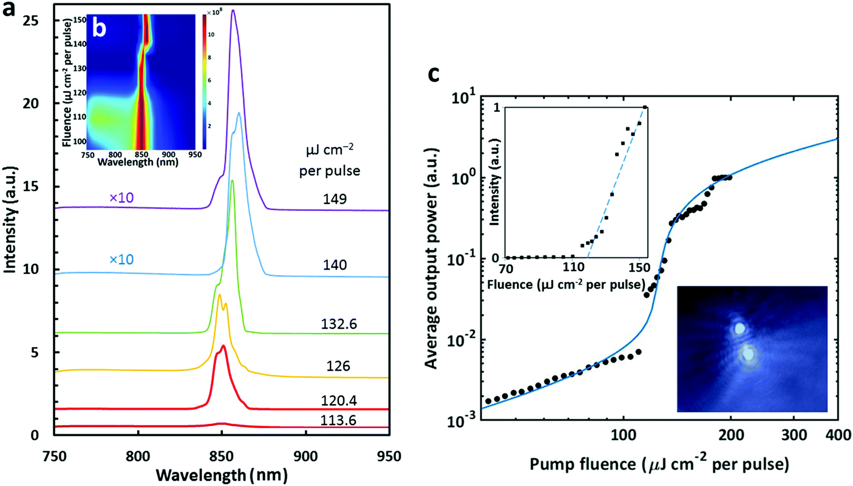 | ||
| Fig. 4 Low temperature lasing of a bare GaAs nanowire. (a) Nanowire emission spectra as a function of pump fluence around the lasing threshold. The emission intensities at 140 and 149 μJ cm−2 per pulse are decreased by factor 10 in the figure. (b) 2D pseudo-colour plot of the normalised emission spectra at different pump fluences, showing a broad emission below the threshold (<120 μJ cm−2 per pulse) and a narrow lasing peak above the threshold (>120 μJ cm−2 per pulse). (c) Logarithmic plot of integrated emission intensity as a function of pump fluence. The extracted S curves from the logarithmic L–L plot are a lasing indication. The top left inset shows the threshold knee behaviour of the linear L–L plot. The bottom right inset shows the optical image of the interference fringes above the threshold. | ||
This is best illustrated in the two-dimensional pseudo-color plot of the normalized emission spectra as a function of excitation power shown in Fig. 4b. At a low pump fluence of 100 μJ cm−2 per pulse, the spectrum has a low intensity peak centered at 850 nm (FWHM ∼ 33 nm) with a broad tail towards shorter wavelengths, which is characteristic of spontaneous emission. The emission appears at longer wavelengths than the PL emission of (bandgap free exciton) ZB GaAs.51 This is attributed to thermal effects due to poor thermal conductivity of the SiO2 substrate and local heating at high pump fluences.
At a pump fluence of 116 μJ cm−2 per pulse, two cavity modes located at 848 and 852 nm start to appear. Above a pump fluence of 120 μJ cm−2 per pulse, the emission intensities increase dramatically and, by deconvolution, the FWHM of each individual peak is estimated to be around 5 nm. With increasing pump fluence to 140 μJ cm−2 per pulse, the two lasing peak positions shift towards longer wavelengths of 858 nm (FWHM ∼ 5 nm) and ∼862 nm (FWHM ∼ 4 nm). For pump fluences higher than 140 μJ cm−2 per pulse, there is a blue shift in the lasing peaks. We attribute the wavelength shifts to an interplay between local heating and gain peak shifts with increasing carrier densities in the nanowire.
Fig. 4c shows the light input–light output plot (L–L curve) of the nanowire laser. The logarithmic L–L plot can be fitted with an S curve using the standard rate equation model (see Section 5.2 of ESI†). The mismatch between the experimental data and analytical fit might be attributed to mode hopping. Mode hopping is manifested as a kink in the linear L–L curve52 (Fig. 4c, top left inset) and a red shift in the lasing peaks53 (Fig. 4b). The bottom right inset image in Fig. 4c shows a representative optical image of the nanowire pumped above the lasing threshold. The spatial interference pattern is characteristic of the axial Fabry–Perot-type cavity. More information about the guided modes supported by our optically pumped GaAs nanowire laser can be found in Section 5.1 of the ESI.†
We note that doping (e.g. with zinc38) has been successfully utilized to enhance the optical properties of VLS grown GaAs nanowires, achieving optically pumped lasing without the need of surface passivation.38,54 To confirm the key role of the side facets in the enhancement of our nanowire optical properties and rule out the possibility of other contributing factors such as doping, the composition of these GaAs nanowires was investigated along the axial and radial directions by atom probe tomography (APT). The APT and also electron dispersive X-ray (EDX) analysis revealed a pure Ga and As composition with no detectable traces of any other elements like silicon or carbon (see Section 6 of the ESI†).
Furthermore, doping relies on a different optical enhancement mechanism than that observed in our nanowires. Doping increases the radiative recombination efficiency, resulting in an increase in PL intensity and quantum efficiency.38,54 However, it does not affect the non-radiative lifetime.38 Our findings reveal that the taper-free {110} GaAs facet nanowires grown via SAE have significantly lower surface recombination and these nanowires display longer non-radiative recombination time.
Room temperature laser operation is desirable for practical devices. We achieved room temperature lasing with GaAs/AlGaAs core/shell nanowires. The optical image obtained at a pump fluence of 105 μJ cm−2 (Fig. 5b) shows strong emission and an interference pattern due to coherent laser emission at the two ends of the nanowire. Fig. 5a shows the evolution in the emission spectrum of a GaAs/AlGaAs nanowire at different pump fluences. The two-dimensional (2D) pseudo-color map of the normalized spectra around the lasing threshold is shown in Fig. 5c. At low pump fluences, the emission peak of the nanowire is broad with a FWHM of ∼42 nm. At a higher pump fluence of 85 μJ cm−2 per pulse, there is a further broadening of the spontaneous emission peak with an FWHM of ∼70 nm. At the pump fluence of 88 μJ cm−2 per pulse, two narrow lasing peaks located at 877 (FWHM ∼ 2 nm) and 880 nm (FWHM ∼ 1.5 nm) appear. At pump fluences above 98 μJ cm−2 per pulse, a rapid increase in the intensities of the lasing peaks is observed with a narrowing of the lasing peaks with FWHMs of less than 3 nm.
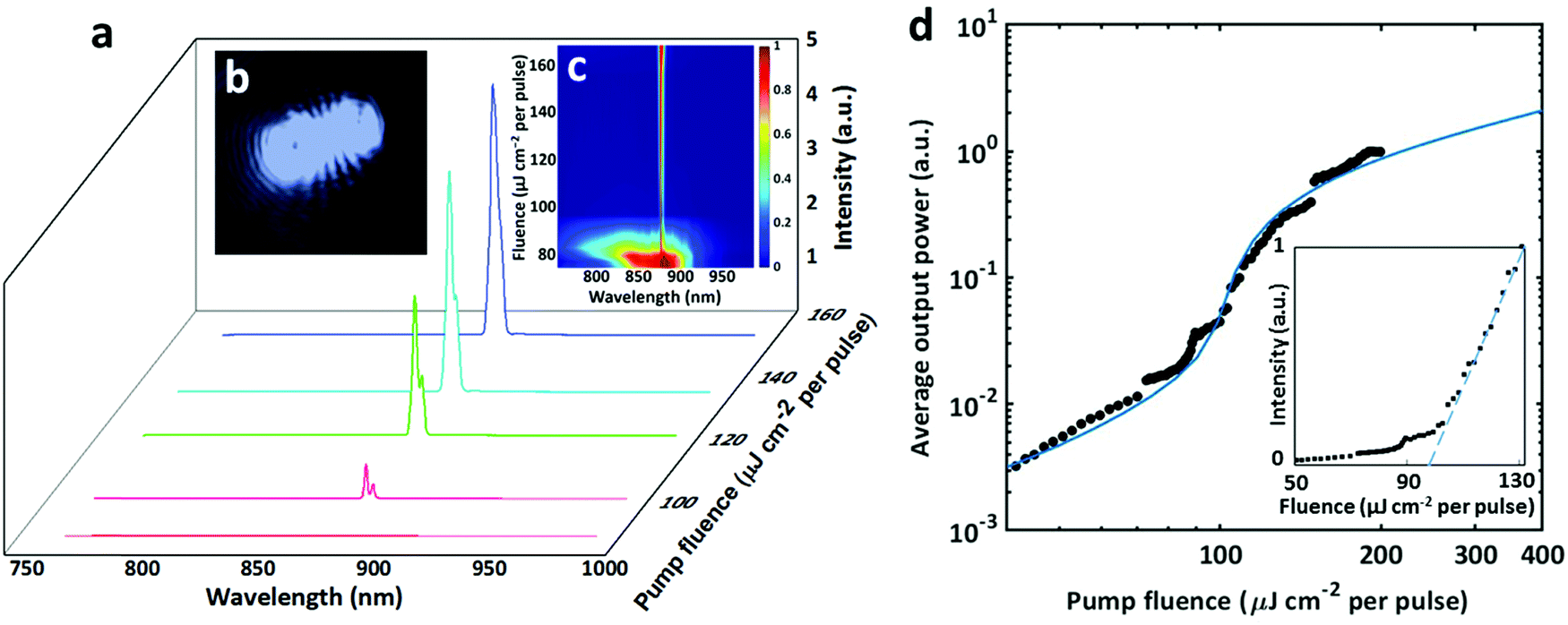 | ||
| Fig. 5 Room temperature lasing of a GaAs/AlGaAs core/shell (passivated GaAs) nanowire. (a) Nanowire emission spectra as a function of pump fluence around the lasing threshold. (b) The left inset shows the optical image of the nanowire at 105 μJ cm−2 per pulse (above the threshold). (c) Normalised spectral map as a function of pump fluence. Note the broad emission below the threshold (<98 μJ cm−2 per pulse) and narrow lasing peak above the threshold (>98 μJ cm−2 per pulse). (d) Logarithmic plot of integrated emission intensity as a function of pump fluence. The S-like shape of this curve is an indication of the nanowire lasing. The inset is the linear plot of (d) showing the threshold knee behaviour. | ||
Fig. 5d shows the experimental light input–light output plot (L–L curve) for the laser. The logarithmic L–L plot shows a non-linear behavior, which can be fitted with an S-curve using the standard rate equation model (Section 5.4 of the ESI†). A knee threshold of 98 μJ cm−2 per pulse is extracted from the linear plot in the linear L–L plot (the inset of Fig. 5d). This is a lower lasing threshold than previously reported for defect-free GaAs/AlGaAs nanowire lasers,35 and Zn+ doped GaAs.38 These studies were from nanowires with similar dimensions under similar excitation conditions. However, it should be noted that the end-facets in these studies are different, and thus can contribute to some variations in lasing.35,38 Above the lasing threshold, there is a blue shift in the lasing peaks with increasing pump fluence. This blue shift is attributed to increased carrier density during stimulated emission.35 Based on the simulation of our GaAs/AlGaAs core/shell nanowires, the TM01 mode has the lowest gain threshold of 273 cm−1 (Fig. S18, ESI†).
The low temperature (8 K) lasing of these bare GaAs nanowires is a testimony to their high optical quality despite the presence of twin defects, noting that lasing has not been reported in defect-free, unpassivated GaAs nanowires grown by VLS. We attribute this superior optoelectronic performance to the low SRV of 3.5 × 104 cm s−1, which is about an order of magnitude lower than previously reported for bare GaAs nanowires with tapered {110}31 and {112} facets44 and two orders of magnitude lower than previously reported for Zn+ doped GaAs nanowires with {111} facets.7,38 The SRV is further reduced to 1.65 × 104 cm s−1 by depositing an AlGaAs passivation layer followed by a GaAs cap. Our GaAs/AlGaAs nanowires lase at room temperature with a low lasing threshold of 98 μJ cm−2 per pulse.
Conclusions
We present a systematic study of the optical and microstructural properties of taper-free GaAs nanowires with {11 0} side facets grown via selective-area metal–organic vapor-phase epitaxy. We demonstrate that the taper-free {110} side facets of these GaAs nanowires result in a very low surface recombination velocity of 3.5 × 104 cm s−1, which is about one order of magnitude smaller than that reported for phase-perfect VLS-grown GaAs nanowires and doped GaAs twinned superlattices. We provide quantitative insights into the contributions of twin defects and side facets on the optical emissions and non-radiative recombination rate in GaAs nanowires, demonstrating the major role of the facets in the optical quality of these nanowires. As a result, despite the presence of twin defects, we demonstrate, for the first time, optically pumped lasing of GaAs nanowires at low temperature (8 K) without surface passivation. We also demonstrate that passivation of these highly performing GaAs nanowires with an AlGaAs shell further reduces the surface recombination velocity to 1.65 × 104 cm s−1, enabling room-temperature lasing with a very low threshold of 98 μJ cm−2 per pulse. We believe that these new insights into the microstructural parameters affecting the performance of GaAs nanowires provide directions for the engineering of efficient optoelectronic components with application in nanoscale lasing and light-emitting devices.Materials and methods
Prior to GaAs nanowire growth, GaAs (111)B substrates were prepared by first depositing 30 nm thick SiO2, followed by array patterning using electron beam lithography and chemical etching of the SiO2 using buffered HF. The prepared substrates were placed in a close coupled showerhead metal organic vapor phase epitaxial reactor with trimethylgallium (TMGa) and arsine (AsH3) used as the precursors of gallium and arsenic, respectively.Nanowires were grown at a temperature of 765 °C and a V/III (AsH3/TMGa) ratio of 20 for 20 min (see growth optimization in the ESI†). The morphology of GaAs nanowires was studied using an FEI-Verios 460 field emission scanning electron microscopy instrument. Their structures were also determined using a JEOL 2100F field emission gun transmission electron microscope. The aberration corrected STEM images were acquired from the FEI Themis Z Advanced Probe Aberration Corrected Analytical TEM/STEM microscope equipped with the Super-X detector system of four silicon drift detectors and a total solid angle of 0.9 srad. The optical properties of the GaAs nanowires were characterized using CL and a home built micro-PL platform. For CL characterization, nanowires were transferred onto a Si substrate with recognizable scribe marks for easy location of individual nanowires. CL mapping and spectroscopic studies were performed at room temperature using a Gatan MonoCL4 Elite CL system attached to a FEI Verios 460 SEM instrument. CL mapping was collected using a current of 1.6 nA and an electron excitation voltage of 5 kV at room temperature and a current of 0.8 nA and an electron excitation voltage of 5 kV at 80 K. For PL measurements, single nanowires were excited through an objective lens (100×) using a 522 nm solid state pulsed laser. Additionally, time-correlated single photon counting was used for carrying out TRPL measurements on the nanowires. The nanowires were photoexcited with a pump fluence of 0.3–15 μJ cm−2 per pulse within a 0.5 μm focal spot of the 100×/0.9 NA objective lens for TRPL measurements. A liquid helium-cooled cryostat adjusted to the micro-PL platform was used for low temperature PL experiments. We investigated the lasing performance of our bare and passivated GaAs nanowires upon transferring them onto a low-index SiO2/Si substrate. The nanowires were optically pumped with a 522 nm pulsed laser, pulse length of 400 fs and repetition rate of 20.8 MHz, with an excitation beam larger than the length of the nanowire (spot size of 13.5 μm).
APT measurement was conducted on a CAMECA LEAP 4000XSi assisted with a 355 nm UV laser pulse system. A detailed specimen preparation can be found in the ESI.† The data were collected at 5 pJ laser energy, 200 kHz laser pulse frequency, 0.5% detection rate and 40 K temperature on the consideration of best signal to noise ratio and longer specimen survival period. The data analysis was carried out in a commercially available software AP suited based on the voltage reconstruction protocol.
Conflicts of interest
There are no conflicts to declare.Acknowledgements
The authors would like to acknowledge the Australian Research Council for financial support. Access to the epitaxial growth, SEM and fabrication facilities were made possible through the Australian National Fabrication Facility, ACT Node. The authors acknowledge the technical and scientific support of the Microscopy Australia node at the University of Sydney (Sydney Microscopy & Microanalysis). We acknowledge Microscopy Australia for access to the TEM at the Centre for Advanced Microscopy at The Australian National University, and thank Mr Wei Wong for scientific discussion and help in the simulation part.References
- P. Caroff, J. Bolinsson and J. Johansson, IEEE J. Sel. Top. Quantum Electron., 2011, 17, 829–846 CAS.
- K. Tomioka, K. Ikejiri, T. Tanaka, J. Motohisa, S. Hara, K. Hiruma and T. Fukui, J. Mater. Res., 2011, 26, 2127–2141 CrossRef CAS.
- K. Hiruma, K. Tomioka, P. Mohan, L. Yang, J. Noborisaka, B. Hua, A. Hayashida, S. Fujisawa, S. Hara, J. Motohisa and T. Fukui, J. Nanotechnol., 2012, 2012(169284), 1–29 Search PubMed.
- R. E. Algra, M. A. Verheijen, M. T. Borgström, L. F. Feiner, G. Immink, W. J. P. Van Enckevort, E. Vlieg and E. P. A. M. Bakkers, Nature, 2008, 456, 369–372 CrossRef CAS PubMed.
- I. Geijselaers, S. Lehmann, K. A. Dick and M. Pistol, Nano Futures, 2018, 2, 035002 CrossRef.
- M. Heiss, S. Conesa-Boj, J. Ren, H. H. Tseng, A. Gali, A. Rudolph, E. Uccelli, F. Peiró, J. R. Morante, D. Schuh, E. Reiger, E. Kaxiras, J. Arbiol and A. Fontcuberta I Morral, Phys. Rev. B: Condens. Matter Mater. Phys., 2011, 83, 1–10 CrossRef.
- T. Burgess, S. Breuer, P. Caroff, J. Wong-Leung, Q. Gao, H. Hoe Tan and C. Jagadish, ACS Nano, 2013, 7, 8105–8114 CrossRef CAS PubMed.
- Z. Ikonic, G. P. Srivastava and J. C. Inkson, Phys. Rev. B: Condens. Matter Mater. Phys., 1995, 52, 14078–14085 CrossRef CAS PubMed.
- J. Bao, D. C. Bell, F. Capasso, J. B. Wagner, T. Mårtensson, J. Trägårdh and L. Samuelson, Nano Lett., 2008, 8, 836–841 CrossRef CAS PubMed.
- D. Spirkoska, J. Arbiol, A. Gustafsson, S. Conesa-Boj, F. Glas, I. Zardo, M. Heigoldt, M. H. Gass, A. L. Bleloch, S. Estrade, M. Kaniber, J. Rossler, F. Peiro, J. R. Morante, G. Abstreiter, L. Samuelson and A. Fontcuberta I Morral, Phys. Rev. B: Condens. Matter Mater. Phys., 2009, 80, 1–9 CrossRef.
- P. Parkinson, H. J. Joyce, Q. Gao, H. H. Tan, X. Zhang, J. Zou, C. Jagadish, L. M. Herz and M. B. Johnston, Nano Lett., 2009, 9, 3349–3353 CrossRef CAS PubMed.
- H. J. Joyce, J. Wong-Leung, Q. Gao, H. Hoe Tan and C. Jagadish, Nano Lett., 2010, 10, 908–915 CrossRef CAS PubMed.
- P. Caroff, K. A. Dick, J. Johansson, M. E. Messing, K. Deppert and L. Samuelson, Nat. Nanotechnol., 2009, 4, 50–55 CrossRef CAS PubMed.
- H. J. Joyce, Q. Gao, H. H. Tan, C. Jagadish, Y. Kim, M. A. Fickenscher, S. Perera, T. B. Hoang, L. M. Smith, H. E. Jackson, J. M. Yarrison-Rice, X. Zhang and J. Zou, Nano Lett., 2009, 9, 695–701 CrossRef CAS PubMed.
- M. Bar-Sadan, J. Barthel, H. Shtrikman and L. Houben, Nano Lett., 2012, 12, 2352–2356 CrossRef CAS PubMed.
- K. Ikejiri, T. Sato, H. Yoshida, K. Hiruma, J. Motohisa, S. Hara and T. Fukui, Nanotechnology, 2008, 19(26), 265604 CrossRef PubMed.
- K. Ikejiri, J. Noborisaka, S. Hara, J. Motohisa and T. Fukui, J. Cryst. Growth, 2007, 298, 616–619 CrossRef CAS.
- H. Yoshida, K. Ikejiri, T. Sato, S. Hara, K. Hiruma, J. Motohisa and T. Fukui, J. Cryst. Growth, 2009, 312, 52–57 CrossRef CAS.
- M. Yao, C. Sheng, M. Ge, C. Y. Chi, S. Cong, A. Nakano, P. D. Dapkus and C. Zhou, ACS Nano, 2016, 10, 2424–2435 CrossRef CAS PubMed.
- K. Tomioka, M. Yoshimura and T. Fukui, Nature, 2012, 488, 189–192 CrossRef CAS PubMed.
- G. Mariani, A. C. Scofield, C. H. Hung and D. L. Huffaker, Nat. Commun., 2013, 4, 1–7 Search PubMed.
- H. Kim, W. J. Lee, T. Y. Chang and D. L. Huffaker, Phys. Status Solidi RRL, 2019, 13, 1–6 Search PubMed.
- P. Senanayake, C. H. Hung, J. Shapiro, A. Lin, B. Liang, B. S. Williams and D. L. Huffaker, Nano Lett., 2011, 11, 5279–5283 CrossRef CAS PubMed.
- C. C. Chang, C. Y. Chi, M. Yao, N. Huang, C. C. Chen, J. Theiss, A. W. Bushmaker, S. Lalumondiere, T. W. Yeh, M. L. Povinelli, C. Zhou, P. D. Dapkus and S. B. Cronin, Nano Lett., 2012, 12, 4484–4489 CrossRef CAS PubMed.
- B. P. Singh, V. S. Baghel and K. S. Baghel, Indian J. Pure Appl. Phys., 2009, 47, 793–803 CAS.
- M. Galicka, M. Bukała, R. Buczko and P. Kacman, J. Phys.: Condens. Matter, 2008, 20(45), 454226 CrossRef.
- Q. Gao, D. Saxena, F. Wang, L. Fu, S. Mokkapati, Y. Guo, L. Li, J. Wong-Leung, P. Caroff, H. H. Tan and C. Jagadish, Nano Lett., 2014, 14, 5206–5211 CrossRef CAS PubMed.
- H. J. Joyce, C. J. Docherty, Q. Gao, H. H. Tan, C. Jagadish, J. Lloyd-Hughes, L. M. Herz and M. B. Johnston, Nanotechnology, 2013, 24, 214006 CrossRef PubMed.
- J. Lloyd-Hughes, S. K. E. Merchant, L. Fu, H. H. Tan, C. Jagadish, E. Castro-Camus and M. B. Johnston, Appl. Phys. Lett., 2006, 89, 232102 CrossRef.
- D. E. Aspnes, Surf. Sci., 1983, 132, 406–421 CrossRef CAS.
- O. Demichel, M. Heiss, J. Bleuse, H. Mariette and A. Fontcuberta i Morral, Appl. Phys. Lett., 2010, 97, 1–4 CrossRef.
- N. Jiang, P. Parkinson, Q. Gao, S. Breuer, H. H. Tan, J. Wong-Leung and C. Jagadish, Appl. Phys. Lett., 2012, 101, 023111 CrossRef.
- H. J. Joyce, P. Parkinson, N. Jiang, C. J. Docherty, Q. Gao, H. H. Tan, C. Jagadish, L. M. Herz and M. B. Johnston, Nano Lett., 2014, 14, 5989–5994 CrossRef CAS PubMed.
- J. Noborisaka, J. Motohisa, S. Hara and T. Fukui, Appl. Phys. Lett., 2005, 87, 093109 CrossRef.
- D. Saxena, S. Mokkapati, P. Parkinson, N. Jiang, Q. Gao, H. H. Tan and C. Jagadish, Nat. Photonics, 2013, 7, 963–968 CrossRef CAS.
- B. Mayer, D. Rudolph, J. Schnell, S. Morkötter, J. Winnerl, J. Treu, K. Müller, G. Bracher, G. Abstreiter, G. Koblmüller and J. J. Finley, Nat. Commun., 2013, 4, 1–7 Search PubMed.
- B. Mayer, L. Janker, B. Loitsch, J. Treu, T. Kostenbader, S. Lichtmannecker, T. Reichert, S. Morkötter, M. Kaniber, G. Abstreiter, C. Gies, G. Koblmüller and J. J. Finley, Nano Lett., 2016, 16, 152–156 CrossRef CAS PubMed.
- T. Burgess, D. Saxena, S. Mokkapati, Z. Li, C. R. Hall, J. A. Davis, Y. Wang, L. M. Smith, L. Fu, P. Caroff, H. H. Tan and C. Jagadish, Nat. Commun., 2016, 7, 1–7 Search PubMed.
- S. Thunich, L. Prechtel, D. Spirkoska, G. Abstreiter, A. Fontcuberta I Morral and A. W. Holleitner, Appl. Phys. Lett., 2009, 95, 26–29 CrossRef.
- X. Yuan, L. Li, Z. Li, F. Wang, N. Wang, L. Fu, J. He, H. H. Tan and C. Jagadish, Nanoscale, 2019, 11, 9207–9215 RSC.
- L. Ahtapodov, H. Kauko, A. M. Munshi, B. O. Fimland, A. T. J. van Helvoort and H. Weman, J. Appl. Phys., 2017, 122, 245102 CrossRef.
- N. Vainorius, D. Jacobsson, S. Lehmann, A. Gustafsson, K. A. Dick, L. Samuelson and M. E. Pistol, Phys. Rev. B: Condens. Matter Mater. Phys., 2014, 89, 1–8 CrossRef.
- J. Bolinsson, M. Ek, J. Trägårdh, K. Mergenthaler, D. Jacobsson, M. E. Pistol, L. Samuelson and A. Gustafsson, Nano Res., 2014, 7, 1–18 CrossRef.
- N. Jiang, J. Wong-Leung, H. J. Joyce, Q. Gao, H. H. Tan and C. Jagadish, Nano Lett., 2014, 14, 5865–5872 CrossRef CAS PubMed.
- E. A. Miller and G. L. Richmond, J. Phys. Chem. B, 1997, 101, 2669–2677 CrossRef CAS.
- R. K. Ahrenkiel, Solid State Electron., 1992, 35, 239–250 CrossRef CAS.
- S. L. Chen, W. M. Chen, F. Ishikawa and I. A. Buyanova, Sci. Rep., 2015, 5, 1–9 CAS.
- D. Rudolph, L. Schweickert, S. Morkötter, L. Hanschke, S. Hertenberger, M. Bichler, G. Koblmüller, G. Abstreiter and J. J. Finley, New J. Phys., 2013, 15, 113032 CrossRef.
- P. Parkinson, H. J. Joyce, Q. Gao, H. H. Tan, X. Zhang, J. Zou, C. Jagadish, L. M. Herz and M. B. Johnston, Nano Lett., 2009, 9, 3349–3353 CrossRef CAS PubMed.
- B. Hua, J. Motohisa, Y. Kobayashi, S. Hara and T. Fukui, Nano Lett., 2009, 9, 112–116 CrossRef CAS PubMed.
- E. H. Bogardus and H. B. Bebb, Phys. Rev., 1968, 176, 993–1002 CrossRef CAS.
- M. Ohtsu and Y. Teramachi, IEEE J. Quantum Electron., 1989, 25, 31–38 CAS.
- X. Tang, J. P. Van Der Ziel, B. Chang, R. Johnson and J. A. Tatum, IEEE J. Quantum Electron., 1997, 33, 927–932 CrossRef CAS.
- J. A. Alanis, M. Lysevych, T. Burgess, D. Saxena, S. Mokkapati, S. Skalsky, X. Tang, P. Mitchell, A. S. Walton, H. H. Tan, C. Jagadish and P. Parkinson, Nano Lett., 2019, 19, 362–368 CrossRef CAS PubMed.
Footnote |
| † Electronic supplementary information (ESI) available. See DOI: 10.1039/d1nh00079a |
| This journal is © The Royal Society of Chemistry 2021 |