
Origin of layer-dependent SERS tunability in 2D transition metal dichalcogenides†
Mingze
Li
 ,
Yimeng
Gao
,
Xingce
Fan
,
Yunjia
Wei
,
Qi
Hao
and
Teng
Qiu
*
,
Yimeng
Gao
,
Xingce
Fan
,
Yunjia
Wei
,
Qi
Hao
and
Teng
Qiu
*
School of Physics, Southeast University, Nanjing 211189, P. R. China. E-mail: tqiu@seu.edu.cn
First published on 5th January 2021
Abstract
Two-dimensional (2D) semiconductors are expected to replace noble metals to become the matrix materials of the next generation of commercial surface-enhanced Raman scattering (SERS) chips. Herein, we systematically studied the influence of the interlayer interaction on the SERS activity of 2D semiconductors from a brand-new perspective and comprehensively analyzed the physicochemical process of 2D semiconductor interlayer modulated SERS. Taking transition metal dichalcogenides as examples, we chose PtSe2 with strong interlayer interactions and ReS2 with weak interlayer interactions to analyze the physicochemical process of 2D semiconductor interlayer modulated SERS by first-principles calculations. PtSe2 and ReS2 samples with various thicknesses were prepared respectively, and the results of comparative experiments proved that the layer-dependent SERS tunability of 2D semiconductors is directly related to the interlayer interaction. This work provided a novel method for further improving the SERS detection limit of 2D semiconductors and a possible strategy for the industrial upgrading of commercial SERS chips.
New conceptsTwo-dimensional (2D) semiconductors are expected to become the matrix materials of the next generation of commercial surface enhanced Raman scattering (SERS) chips because of their atomic-level flatness and excellent photoelectric properties. Limited by the unsatisfactory SERS detection limit of 2D semiconductors, the development of simple technology and performance that is not inferior to noble metals has become an important issue for the innovation of commercial 2D semiconductor SERS chips. As one of the important factors affecting the properties of 2D materials, interlayer interaction has not been studied in depth in the field of SERS. Herein, we explored the influence of interlayer interaction on SERS performance by using 2D PtSe2 and ReS2 with different numbers of layers as the research objects. The results of density functional theory calculations and comparative experiments proved that the layer-dependent SERS tunability of 2D semiconductors is directly related to the interlayer interaction. This work not only explained the influences of interlayer interaction on SERS, but also deepened our understanding of the origin of 2D semiconductor layer-dependent SERS tunability, providing a novel insight for further improving the SERS detection limit of 2D semiconductors. |
As an important field of surface science, surface-enhanced Raman scattering (SERS) has been extensively applied in various areas such as the in situ monitoring of nano-catalysis reactions,1–3 single molecule detection4–7 and viable cell detection.8–10 Correspondingly, SERS active substrates have always been one of the research focuses.11 In recent years, the discovery of low dimensional semiconductor SERS substrates with noble-metal-comparable SERS performance has opened a new chapter for SERS research.12 The SERS of low dimensional semiconductors is hardly explained by the pre-existing surface concepts due to the diverse enhancement mechanisms. For example, by introducing defects such as replaced atoms,13 grain boundaries,14 and vacancies,15,16 we can adjust the photo-induced charge transfer (PICT) process between the materials and adsorbent molecules with the help of the corresponding defect energy, thus enhancing the Raman scattering of adsorbent molecules on the low dimensional materials.17 Beyond that, another strategy is changing the interface interaction to realize the regulation of the energy bands and the surface charge doping of the semiconductors, aiming at realizing Raman enhancement.18
Due to the inherent drawbacks of the zero-dimensional and one-dimensional materials, including the difficulty in synthesis, hard planarization and inhomogeneous SERS activity, there is a long way to go before commercialization. In contrast, the two-dimensional (2D) materials exhibit evident superiority. On the one hand, the flat crystal of 2D semiconductors allows uniform chemisorbed molecules for obtaining stable and repeatable Raman signals,19 which is essential to the practical applications. On the other hand, 2D semiconductors are easy to prepare and modulate. Using this, we can combine the specific functions of different materials freely, therefore constructing commercial SERS substrates.20,21 Relevant technologies such as alloy doping,22 defect regulation23 and surface engineering14 have been successfully employed in the 2D semiconductor SERS substrates. In the previous work, we found that 2D semiconductor materials with different layers make a sharp distinction in the SERS enhancement factor.24–26 But unfortunately, to the best of our knowledge, there has not been systematic research to explain the cause of this phenomenon.
The interlayer interaction of 2D semiconductors is mainly dominated by the van der Waals (vdw) forces, which originate from the coherent electronic waves between molecules.27 Though weaker than the electrostatic interaction or hydrogen bonds, vdw force, as a kind of long-range interaction generally existing in molecular systems, plays an important role in the noncovalent bonding.28 We speculated that the layer-dependent SERS tunability of 2D semiconductor substrates mainly comes from the interlayer interaction. Taking the 2D transition metal dichalcogenides (TMDs) as an example, the interlayer interaction of PtSe2 is strong and that of ReS2 is relatively weak. As for the low dimensional semiconductors, research on the PICT mechanism usually takes the energy band structure as the starting point and analyzes the process based on the charge transfer model proposed by Professor Lombardi.17 Hence, we further surmised that the layer-dependent SERS tunability of the PtSe2 and ReS2 films would present a bigger difference due to their different degrees of interlayer interaction.
PtSe2, a rising member of the group-10 transition metal dichalcogenides family, has been demonstrated to have a strong interlayer interaction.29,30 It possesses many intriguing properties and good environmental stability, indicating the enormous potential in SERS application.31 Besides, one of the typical materials with weak interlayer interactions is 2D ReS2.32 As a direct gap semiconductor, the valence band and conduction band edges of ReS2 are composed of d-orbitals of Re atoms and p-orbitals of S atoms, respectively. Due to the charge decoupling of an extra valence electron from Re-atoms, ReS2 crystallizes in a distorted 1T diamond-chain structure. This distortion in crystal structure would weaken the coupling between layers. Consequently, the overlapping of electron wavefunctions from adjacent layers is so weak that a modulation of the interlayer distance cannot renormalize the band structure, implying that ReS2 is electronically decoupled.33
Derived from the interaction between atoms from different layers, interlayer interaction could directly cause the charge redistribution, which further affects the coupling of the material surface and molecules for the 2D TMD SERS substrates. Fig. 1a displays the interlayer differential charge density of bilayer PtSe2 calculated by density functional theory (DFT). From the results, we found that a lot of electrons are bound between layers and distributed around Pt atoms, indicating strong interlayer interaction. Such strong interlayer interaction is a result of the hybridization of the pz orbital of interlayer Se atoms in PtSe2.29 Moreover, DFT calculations were also used to study the coupling of analytes and PtSe2 with different thicknesses (Fig. 1c and e). Methylene blue (MeB) is one of the typical probe molecules used to detect the SERS performance of different substrates; therefore, the binding energy of MeB with different systems was simulated as an example. Greater binding energy signified a stronger interface dipole between the material and molecules, which played a positive role in the SERS process. The binding energy of MeB with monolayer (1L) PtSe2 was calculated to be 3.76 eV, much larger than that of MeB with bilayer (2L) PtSe2 (3.15 eV), suggesting stronger coupling between MeB and the PtSe2 films with fewer layers. The detailed calculation results are shown in Table S1 (ESI†). As for bilayer ReS2, the interlayer differential charge density is shown in Fig. 1b. Wherein, little change appears in the distribution of electrons between layers compared with the monolayer one, which indicates that the binding energies of surface molecules absorbed on 1L ReS2 and 2L ReS2 are approximately equal (1.95 eV for MeB-1L ReS2 and 1.86 eV for MeB-2L ReS2, see Fig. 1d and f). In other words, due to the weak interlayer interaction, the binding energy of 2D ReS2 hardly changes when the number of layers increases, in sharp contrast to PtSe2.
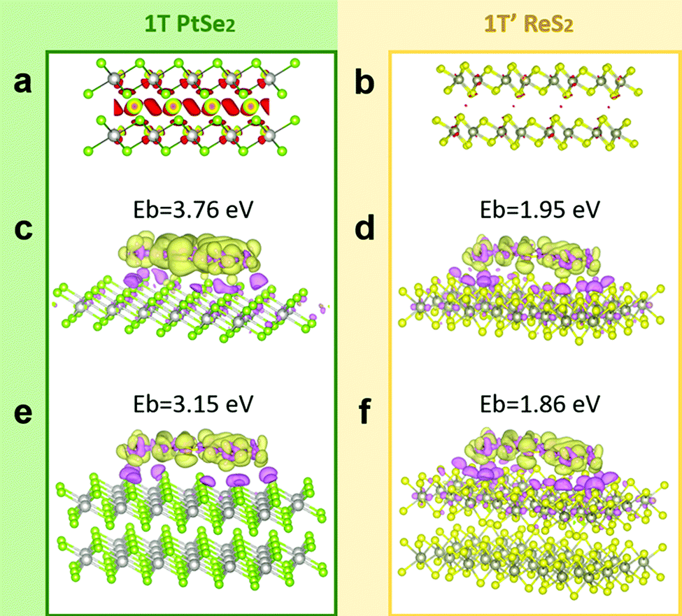 | ||
| Fig. 1 The interlayer differential charge density of bilayer PtSe2 (a) and bilayer ReS2 (b) calculated by DFT. Side views of the electron density difference isosurface (0.00036 electron bohr−3) for MeB molecules absorbed on 1L PtSe2 (c), 2L PtSe2 (e), 1L ReS2 (d), and 2L ReS2 (f). The binding energy of these systems was calculated respectively. | ||
Based on the above simulation analysis, we suggest that the interlayer interaction has a great modulation effect on SERS of 2D materials, especially TMDs. In order to show the enhanced mechanism more clearly, we calculated the band structure of PtSe2 and ReS2 with different layers by first-principles calculations. We find that when increasing the layers of TMDs, the influence of interlayer reaction is gradually highlighted, especially in the band structure. For PtSe2 with strong interlayer interactions, the band gap shrinks obviously with an increase in layer number. For example, the band gaps for 1L, 2L, three-layer (3L) and bulk PtSe2 are 1.35 eV, 0.89 eV, 0.76 eV and 0 eV, respectively (Fig. 2a and c). Similar phenomena were found in other semiconductor phase TMD materials. For example, when the number of WS2 layers increases, its exciton energy also decreases significantly. However, as the interlayer interaction of WS2 is weaker than that of PtSe2, its exciton energy decreases less with the increase of layers.34 While for ReS2 with weak interlayer interactions, there is almost no change in the band structure with the variation of the layer number. As Fig. 2b and d show, the energy gaps at the highly symmetric point Γ for 1L, 2L, 3L and bulk ReS2 are 1.44 eV, 1.40 eV, 1.35 eV and 1.32 eV respectively, which leads to an inconspicuous decline in the exciton resonance intensity.
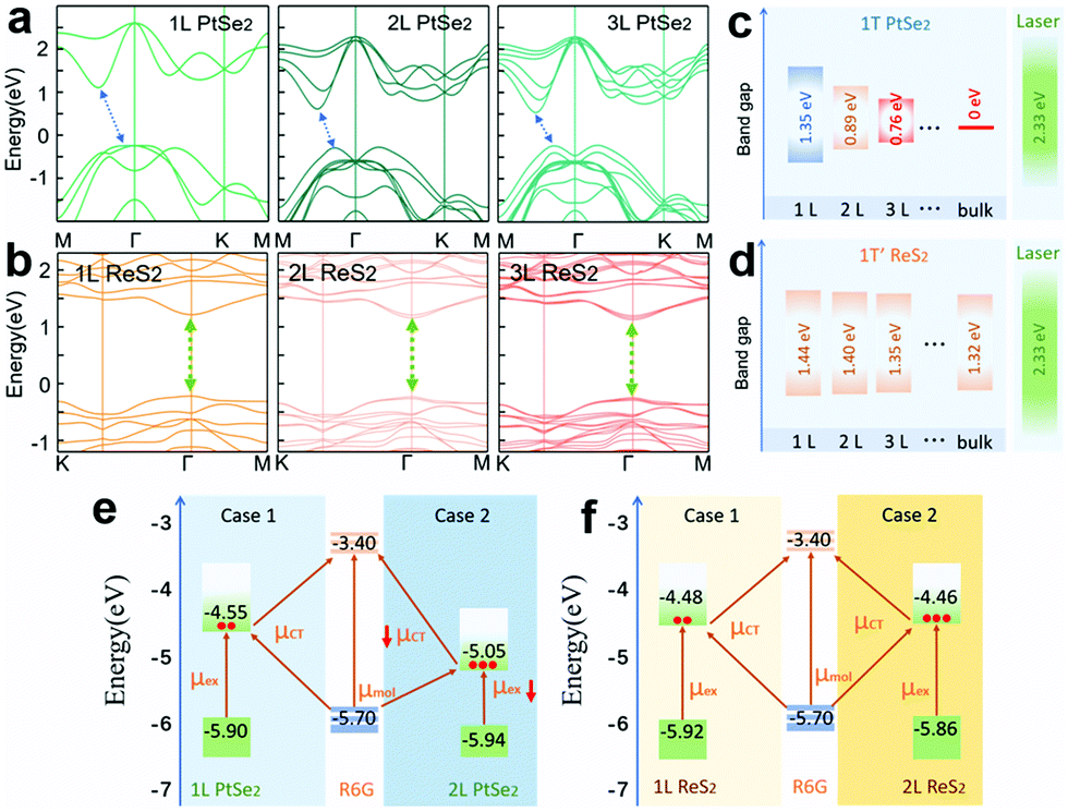 | ||
| Fig. 2 The calculated band structure of 1L, 2L, 3L PtSe2 (a) and 1L, 2L, 3L ReS2 (b). The energy gap at point Γ of PtSe2 (c) and ReS2 (d) from 1L to bulk. (e and f) Schematic illustration of the PICT process of the PtSe2-R6G system and ReS2-R6G system while the number of layers increased. | ||
According to the chemically enhanced mechanism of SERS, the most intense SERS enhancement occurs for transitions terminating at the band edge. The intensity of the Raman spectra is proportional to the polarizability tensor and the polarization tensor is generally expressed as α = A + B + C, where A is relevant to the molecular resonance, and B and C represent the contribution of charge-transfer between the molecules and semiconductor, including a PICT process.17 Since the most crucial charge transfer process can borrow intensity from molecular resonances (μmol) or exciton resonances (μex), the PICT process would be simultaneously weakened while μex was dropped off, leading to a decrease in SERS signal strength.
In order to illustrate the above SERS procedure, we analyzed the PICT process based on the relative position of the energy bands in the typical probe Rhodamine 6G (R6G) molecule to the materials. In terms of PtSe2, the indirect energy gap turns from 1.35 eV to 0.89 eV when adding an extra layer to the monolayer material (see Fig. 2e). With a distinct mismatch between the gap and the exciting light at 532 nm, the μex in 2L PtSe2 is attenuated sharply, consequently weakening the corresponding PICT process. Different from PtSe2, the gap of 2L ReS2 alters very little compared with 1L ReS2 (Fig. 2f). Hence the PICT between molecules and 2L ReS2 is merely abated slightly. The results are similar when MeB was treated as an example (Fig. S1, ESI†).
The above theoretical results indicate that the SERS tunability in 2D TMDs probably originates from the interlayer interaction and the stronger the interaction is, the larger the degree of regulation that can be attained. The analysis made us firmly believe that the interlayer interaction is important to SERS of 2D materials, especially TMDs, and on this theoretical prediction, we designed a comparative experiment to verify our assumption. At first, a series of high-quality samples were prepared and characterized (Fig. S2, ESI†). The schematic illustration of the measurement procedure and the photograph of the PtSe2 films is presented in Fig. 3a and b. As illustrated by Fig. 3b, the 2D PtSe2 films were synthesized on a sapphire substrate, wherein the dark blue region represents 2D PtSe2 and the light blue region refers to the sapphire substrate. In addition, it showed that the film fits well with the substrate and has a uniform surface. To measure the binding energy of 2D PtSe2 films, we observed X-ray photoelectron spectroscopy (XPS), illustrated in Fig. 3c. As a result, the fitted peak positions are 72.96 eV, 76.28 eV for Pt 4f and 54.31 eV, 55.16 eV for Se 3d, respectively, which are consistent with previous reports.35 Hardly any oxides, unreacted Pt metal and Se substance were evidenced by the Pt 4f and Se 3d core levels, indicating the good quality of the 2D PtSe2 films. Fig. 3d displays the Raman spectrum of 2D PtSe2 films with laser excitation at 532 nm, in which the two prominent peaks at ∼178 and ∼210 cm−1 correspond to Eg (in plane) and A1g (out of plane) vibrations of Se atoms respectively and the peak at ∼230 cm−1 can be attributed to a longitudinal optical (LO) mode.36 Besides, the peaks marked by light blue (414 cm−1, 576 cm−1 and 749 cm−1) are supposed to be the characteristic peaks of Al2O3. In addition, using R6G and MeB as SERS probe molecules, we found that the grown 2D PtSe2 films had obvious SERS performance (Fig. 3e and Fig. S3, ESI†), which was convenient for us to make subsequent comparison. By regulating the growth time, we have prepared four types of PtSe2 films with different thicknesses, named as S1, S2, S3 and S4. The thicknesses of these PtSe2 films are in the range of 1 to 5 nm measured by atomic force microscopy (AFM), as shown in Fig. 3f. The bandgaps of S1 to S4 are estimated to be 1.22 eV, 0.72 eV, 0.65 eV and 0.49 eV, respectively, by the Tauc plots of the layer-dependent PtSe2 (Fig. S4, ESI†). Additionally, we can apply the SERS theory for semiconductors to analyze the 2D 1T PtSe2 films because of their semiconductor nature.
 | ||
| Fig. 3 (a) Schematic illustration of the measurement procedure and prepared samples including 1L PtSe2 and 2L PtSe2. (b) Photograph of the PtSe2 film grown on the sapphire substrate and the optical microscope image of typical PtSe2 flakes. (c) XPS spectra for Pt 4f and Se 3d of 2D PtSe2 film. (d) Raman spectrum of the 2D PtSe2 on the sapphire substrate. (e) Typical Raman spectra of 10−5 M R6G absorbed on the 2D PtSe2 and the sapphire substrate. (f) The AFM topographic image of PtSe2 with different thicknesses, named as S1, S2, S3 and S4. The inset supplements the thickness of each sample. | ||
Fig. 4a schematically illustrates the Raman measurement of 1L ReS2 and 2L ReS2. As shown in Fig. 4b, a continuous ReS2 film was grown on the sapphire substrate, according to the observation under a microscope. The low crystal symmetry of the distorted 1T phase of ReS2 results in the emergence of more than 5 strong Raman peaks in the range of 100–450 cm−1. Wherein, Raman peaks at 150, 161, 211, 232, and 306 cm−1 belong to in plane Eg-like mode, and the peak at 139 cm−1 is attributed to an out-of-plane A1g-like mode. Other Raman modes located beyond 300 cm−1 are mostly contributed by the vibrations of S atoms37 (Fig. 4c). The XPS spectrum of Re 4f indicates the good quality of ReS2 films (Fig. S5, ESI†). Similar to PtSe2, we also fabricated these types of ReS2 films with the thickness ranging from 0.7 to 3 nm, named as W1, W2 and W3 (Fig. 4d). Fig. 4e displays that random samples demonstrated excellent SERS performance.
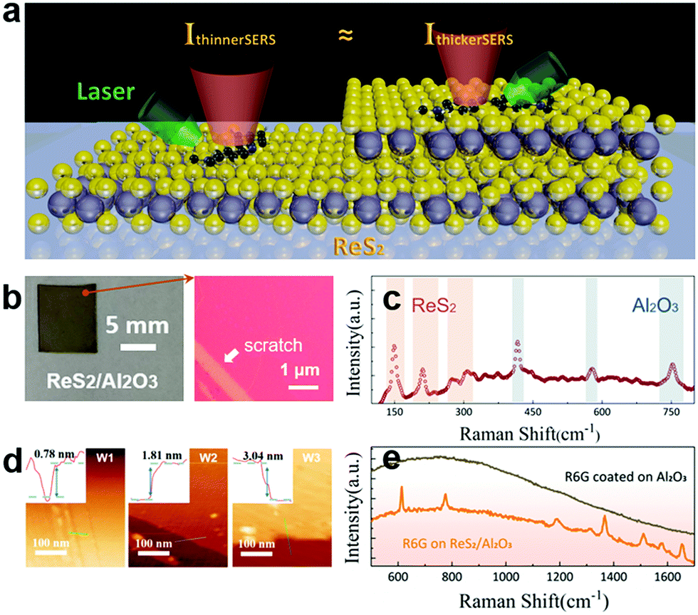 | ||
| Fig. 4 (a) Schematic illustration of the measurement procedure and prepared samples including 1L ReS2 and 2L ReS2. (b) Photograph of the ReS2 film grown on the sapphire substrate and the optical microscope image of typical ReS2 flakes. (c) Raman spectrum of the 2D ReS2 on the sapphire substrate. (d) The AFM topographic image of ReS2 with different thicknesses, named as W1, W2 and W3. The inset supplements the thickness of each sample. (e) Typical Raman spectra of 10−5 M R6G absorbed on the 2D ReS2 and the sapphire substrate. | ||
In the process of characterizing different samples we found that in the Raman spectra of PtSe2, the A1g peak is significantly enhanced as the layers added, indicating the strengthened out-of-plane vibration mode due to the strong interlayer interaction30 (Fig. 5a). All the Raman peaks of ReS2 films, including the A1g peak, almost exhibited no response to the changes of thickness (Fig. 5b). This is because the weak interlayer interaction of ReS2 renders all the vibration modes nearly invariable with the layer number altered, in agreement with previous reports. Using R6G as probe molecules, we measured the Raman spectra on all the PtSe2 and ReS2 samples under identical conditions. We randomly selected 20 points for each type of substrates and averaged the signals to get the SERS spectra of R6G on different substrates (Fig. 5c and d). It can be proven by UV-Vis absorption spectra that the Raman enhancement is attributed to a chemical mechanism, and a detailed explain has been shown in Fig. S6 (ESI†). Meanwhile, in order to show the trend of signal changes more intuitively, we extracted the average signal intensities integrated at 612 cm−1, 773 cm−1 and 1365 cm−1 for each type of substrates separately and collected them in Fig. 5e and f. The results are similar when MeB was used as the probe molecule (Fig. S7, ESI†). The experiment results reveal that both PtSe2 and ReS2 possess layer-dependent SERS tunability with a decrease in SERS ability as the layers added. What's more, directly related to the interlayer interaction, the descent extent becomes larger when the interaction is strong, which completely coincides with the theoretical calculations. With the increase of the layer numbers, the amplitude of each change caused by the interlayer interaction gradually decreased, and the amplitude of SERS tunability also decreased gradually.
 | ||
| Fig. 5 Characteristic Raman spectra of (a) PtSe2 films (S1 to S4) and (b) ReS2 films (W1 to W3). Enhanced Raman spectra of 10−5 M R6G on the (c) PtSe2 films (S1 to S4) and (d) ReS2 films (W1 to W3). The extracted average signal intensities integrated at 612 cm−1, 773 cm−1 and 1365 cm−1 for S1 to S4 (e) and W1 to W3 (f). | ||
Conclusions
In summary, we explored the influence of interlayer interaction on the SERS performance by using 2D PtSe2 and ReS2 with different numbers of layers as the research objects. Both experimental and DFT simulated results unveil that the layer-dependent SERS effects of 2D TMDs mainly depend on the interlayer coupling of TMD substrates. For the ones exhibiting weak interlayer interactions, such as ReS2, increasing the number of layers has little effect on its surface properties and the electronic band structure. As a result, the intensity of the SERS signals is almost unchanged on different ReS2 films with nanoscale thickness variation. For TMDs with strong interlayer interactions, take PtSe2 as an example. On the one hand, the properties of the multilayer structure are significantly altered by the interlayer interaction when the layers are added, which includes the contraction of the electronic band gap and the decrease of the exciton energy, working together to impede the exciton resonance process. On the other hand, the interlayer interaction changes the charge distribution inside the TMDs, making the coupling between the surface and molecules become weak with the increase of layers. All of the above changes caused by the interlayer interaction contribute to the layer-dependent SERS tunability of 2D TMDs. This work not only explained the influences of interlayer interaction on SERS, but also deepened our understanding of the origin of 2D TMDs layer-dependent SERS tunability, providing a reference and new ideas for the property modulation of other related materials.Conflicts of interest
There are no conflicts to declare.Acknowledgements
This work was supported by the National Natural Science Foundation of China (Grant No. 11874108) and the National Key R&D Program of China (Grant No. 2017YFA0403600).References
- X. Huang, C. Tang, J. Li, L. C. Chen, J. Zheng, P. Zhang, J. Le, R. Li, X. Li and J. Liu, Sci. Adv., 2019, 5, eaaw3072 CrossRef CAS.
- E. Cortés, W. Xie, J. Cambiasso, A. S. Jermyn, R. Sundararaman, P. Narang, S. Schlücker and S. A. Maier, Nat. Commun., 2017, 8, 1–10 CrossRef.
- H. Zhang, S. Duan, P. M. Radjenovic, Z. Q. Tian and J. F. Li, Acc. Chem. Res., 2020, 53, 729–739 CrossRef CAS.
- K. Kneipp, Y. Wang, H. Kneipp, L. T. Perelman, I. Itzkan, R. R. Dasari and M. S. Feld, Phys. Rev. Lett., 1997, 78, 1667 CrossRef CAS.
- D. K. Lim, K.-S. Jeon, H. M. Kim, J.-M. Nam and Y. D. Suh, Nat. Mater., 2010, 9, 60–67 CrossRef CAS.
- C. Y. Li, S. Duan, J. Yi, C. Wang, P. M. Radjenovic, Z. Q. Tian and J. F. Li, Sci. Adv., 2020, 6, eaba6012 CrossRef CAS.
- D. J. Liu, T. T. Wu, Q. Zhang, X. M. Wang, X. Y. Guo, Y. K. Su, Y. Zhu, M. H. Shao, H. J. Chen, Y. Luo and D. Y. Lei, ACS Nano, 2019, 13(7), 7644–7654 CrossRef CAS.
- L. F. Tadesse, C.-S. Ho, D.-H. Chen, H. Arami, N. Banaei, S. S. Gambhir, S. S. Jeffrey, A. A. Saleh and J. A. Dionne, Nano Lett., 2020, 20, 7655–7661 CrossRef CAS.
- J.-H. Choi, T.-H. Kim, W. A. El-Said, J.-H. Lee, L. Yang, B. Conley, J.-W. Choi and K.-B. Lee, Nano Lett., 2020, 20, 7670–7679 CrossRef CAS.
- A. F. Chrimes, K. Khoshmanesh, S.-Y. Tang, B. R. Wood, P. R. Stoddart, S. S. E. Collins, A. Mitchell and K. Kalantar-zadeh, Biosens. Bioelectron., 2013, 49, 536–541 CrossRef CAS.
- P. L. Stiles, J. A. Dieringer, N. C. Shah and R. P. Van Duyne, Annu. Rev. Anal. Chem., 2008, 1, 601–626 CrossRef CAS.
- S. Cong, Y. Yuan, Z. Chen, J. Hou, M. Yang, Y. Su, Y. Zhang, L. Li, Q. Li and F. Geng, Nat. Commun., 2015, 6, 7800 CrossRef CAS.
- Z. Zheng, S. Cong, W. Gong, J. Xuan, G. Li, W. Lu, F. Geng and Z. Zhao, Nat. Commun., 2017, 8, 1–10 CrossRef CAS.
- R. Rani, A. Yoshimura, S. Das, M. R. Sahoo, A. Kundu, K. K. Sahu, V. Meunier, S. K. Nayak, N. Koratkar and K. S. Hazra, ACS Nano, 2020, 14, 6258–6268 CrossRef CAS.
- C. Muehlethaler, C. R. Considine, V. Menon, W.-C. Lin, Y.-H. Lee and J. R. Lombardi, ACS Photonics, 2016, 3, 1164–1169 CrossRef CAS.
- H. T. Chen, S. J. Xiong, X. L. Wu, J. Zhu, J. C. Shen and P. K. Chu, Nano Lett., 2009, 9, 1926–1931 CrossRef CAS.
- J. R. Lombardi and R. L. Birke, J. Phys. Chem. C, 2014, 118, 11120–11130 CrossRef CAS.
- Z. Hu, Z. Wu, C. Han, J. He, Z. Ni and W. Chen, Chem. Soc. Rev., 2018, 47, 3100–3128 RSC.
- Q. Ding, J. Wang, X. Chen, H. Liu, Q. Li, Y. Wang and S. Yang, Nano Lett., 2020, 20, 7304–7312 CrossRef CAS.
- Y. Tan, L. Ma, Z. Gao, M. Chen and F. Chen, Nano Lett., 2017, 17, 2621–2626 CrossRef CAS.
- M. Li, X. Fan, Y. Gao and T. Qiu, J. Phys. Chem. Lett., 2019, 10, 4038–4044 CrossRef CAS.
- X. Hou, X. Zhang, Q. Ma, X. Tang, Q. Hao, Y. Cheng and T. Qiu, Adv. Funct. Mater., 2020, 30, 1910171 CrossRef CAS.
- J. Seo, J. Lee, Y. Kim, D. Koo, G. Lee and H. Park, Nano Lett., 2020, 20, 1620–1630 CrossRef CAS.
- X. Song, Y. Wang, F. Zhao, Q. Li, H. Q. Ta, M. H. Rümmeli, C. G. Tully, Z. Li, W.-J. Yin and L. Yang, ACS Nano, 2019, 13, 8312–8319 CrossRef CAS.
- L. Tao, K. Chen, Z. Chen, C. Cong, C. Qiu, J. Chen, X. Wang, H. Chen, T. Yu and W. Xie, J. Am. Chem. Soc., 2018, 140, 8696–8704 CrossRef CAS.
- C. Weng, Y. Luo, B. Wang, J. Shi, L. Gao, Z. Cao and G. Duan, J. Mater. Chem. C, 2020, 8, 14138–14145 RSC.
- P. Ajayan, P. Kim and K. Banerjee, Phys. Today, 2016, 69, 38 CrossRef CAS.
- K. S. Novoselov, O. A. Mishchenko, O. A. Carvalho and A. C. Neto, Science, 2016, 353, 6298 CrossRef.
- Y. Zhao, J. Qiao, P. Yu, Z. Hu, Z. Lin, S. P. Lau, Z. Liu, W. Ji and Y. Chai, Adv. Mater., 2016, 28, 2399–2407 CrossRef CAS.
- X. Chen, S. Zhang, L. Wang, Y.-F. Huang, H. Liu, J. Huang, N. Dong, W. Liu, I. M. Kislyakov and J. M. Nunzi, Photonics Res., 2019, 7, 1416–1424 CrossRef CAS.
- Y. Zhao, J. Qiao, Z. Yu, P. Yu, K. Xu, S. P. Lau, W. Zhou, Z. Liu, X. Wang and W. Ji, Adv. Mater., 2017, 29, 1604230 CrossRef.
- M. Rahman, S. Qiao and K. Davey, Adv. Funct. Mater., 2017, 27, 1606129 CrossRef.
- S. Tongay, H. Sahin, C. Ko, A. Luce, W. Fan, K. Liu, J. Zhou, Y.-S. Huang, C.-H. Ho and J. Yan, Nat. Commun., 2014, 5, 1–6 Search PubMed.
- C. T. Yip, T. W. Lo, S. C. Zhu, G. Y. Jia, H. R. Sun, C. H. Lam and D. Y. Lei, Tight-binding modeling of excitonic response in van der Waals stacked 2D semiconductors, Nanoscale Horiz., 2019, 4, 969 RSC.
- Y. Wang, L. Li, W. Yao, S. Song, J. T. Sun, J. Pan, X. Ren, C. Li, E. Okunishi and Y.-Q. Wang, Nano Lett., 2015, 15, 4013–4018 CrossRef CAS.
- L. Wang, S. Zhang, N. McEvoy, Y. Sun, J. Huang, Y. Xie, N. Dong, X. Zhang, I. M. Kislyakov and J.-M. Nunzi, Laser Photonics Rev., 2019, 13, 1900052 CrossRef.
- M. Hafeez, L. Gan, H. Li, Y. Ma and T. Zhai, Adv. Funct. Mater., 2016, 26, 4551–4560 CrossRef CAS.
Footnote |
| † Electronic supplementary information (ESI) available: The methods of samples synthesis, Raman measurements and DFT calculations; the detailed binding energy of different systems; schematic illustration of the PICT process of the PtSe2-MeB system and ReS2-MeB system; basic character of 1T PtSe2 and 1T’ ReS2; the enhanced Raman spectra of Methyl blue (MB) and MeB on S1; the Tauc plots of PtSe2 with different thicknesses; the XPS spectrum for Re of ReS2 film; the UV-Vis absorption of PtSe2 with different thicknesses; enhanced Raman spectra of MeB on the PtSe2 films (S1 to S4) and ReS2 films (W1 to W3). See DOI: 10.1039/d0nh00625d |
| This journal is © The Royal Society of Chemistry 2021 |