
Intrinsic spin–valley-coupled Dirac state in Janus functionalized β-BiAs monolayer†
Zhifeng
Liu
 *a,
Lingjun
Li
a,
Leyuan
Cui
a,
Yongting
Shi
a,
Tielei
Song
a,
Jiangtao
Cai
b,
Xin
Cui
a,
Xue
Jiang
c and
Jijun
Zhao
*c
*a,
Lingjun
Li
a,
Leyuan
Cui
a,
Yongting
Shi
a,
Tielei
Song
a,
Jiangtao
Cai
b,
Xin
Cui
a,
Xue
Jiang
c and
Jijun
Zhao
*c
aSchool of Physical Science and Technology, Inner Mongolia University, Hohhot 010021, China. E-mail: zfliu@imu.edu.cn
bDepartment of Physics, Shaanxi University of Science & Technology, Xi’an 710021, China
cKey Laboratory of Materials Modification by Laser, Ion and Electron Beams (Dalian University of Technology), Ministry of Education, Dalian 116024, China. E-mail: zhaojj@dlut.edu.cn
First published on 22nd January 2021
Abstract
Recently, a new class of 2D Dirac materials, spin–valley-coupled Dirac semimetals (svc-DSMs), was proposed in strained SbAsX2 monolayers (MLs) and transition metal dichalcogenide-supported graphene. Owing to the superb properties, including Dirac spin–valley Hall effect and dissipationless transport, svc-DSMs provide an ideal platform for exploring the integration of Dirac physics, spintronics and valleytronics. However, the predicted candidate materials are all extrinsic, requiring tensile strain or proximity effect. Using first-principles calculations, herein we identify that strain-free BrBiAsCl ML is an intrinsic svc-DSM that is located at the boundary between 2D trivial insulators and topological insulators owing to the balance between spin–orbit coupling (SOC) and the built-in polarized vertical electric field. Under inversion asymmetry, the strong SOC in BrBiAsCl ML induces giant spin-splittings in both the uppermost valence band and the lowermost conduction band, rendering a nearly closed bulk gap and the formation of a spin–valley-dependent Dirac cone. Remarkably, such an svc-DSM state can be well preserved in BrBiAsCl ML when supported on a proper substrate, which is indispensable for the application of svc-DSMs in devices.
New conceptsFor realizing the pursued integration of Dirac physics, spintronics and valleytronics, it is essential to have an intrinsic spin–valley-coupled Dirac semimetal (svc-DSM) hosting both spin and valley polarized massless fermions without external modulation. In this communication, we proposed to design an intrinsic svc-DSM by Janus functionalization, which can greatly expand the possible strength of the built-in polarized vertical electric field (VEF) to reach a balance between spin–orbit coupling and VEF. Following this guidance, we predicted the first candidate 2D material of intrinsic svc-DSM, namely, Janus BrBiAsCl monolayer, which has inversion asymmetry and satisfactory stability. Our finding opens a new route for the design, synthesis, and spintronic device applications of svc-DSM. |
1. Introduction
As exemplified by graphene with massless Dirac fermions,1 novel 2D Dirac materials (DMs) hold great promise for superfast and ultra-low-power electronic and spintronic devices.2–8 According to the influence of spin–orbit coupling (SOC), the reported 2D DMs with time-reversal symmetry can be divided into three classes. The typical class is graphene-like DMs (e.g., silicene,3 graphynes4 and phagraphene5), whose linear Dirac crossings will be gapped by SOC; therefore, they are in essence 2D topological insulators, in which the bulk gap harbors a gapless edge state. Another class is spin–orbit DMs such as 2D HfGeTe,9 in which the Dirac points cannot be gapped by SOC owing to the nonsymmorphic space group symmetry.10 Recently, a new class of 2D DMs, namely, spin–valley-coupled Dirac semimetals (svc-DSMs), has been proposed.11 In the absence of SOC, svc-DSMs are semiconductors with a modest bandgap. When SOC is considered, however, distinct Dirac states are formed owing to the giant spin-splittings induced by strong SOC and inverse asymmetry. Since the spin moment and Berry curvature are opposite in inequivalent valleys, there is a Dirac spin–valley Hall effect in svc-DSMs, giving rise to a constant spin Hall conductivity along with massless and dissipationless charge carrier transport. Based on first-principles calculations, a series of functionalized V–V binary 2D materials, SbAsX2 (X = H, F, Cl, Br, I) monolayers (MLs),11 have been identified as the candidates for svc-DSMs. However, the svc-DSM state in SbAsX2 MLs is not intrinsic, and biaxial strains of 2.3% to 9.2% tensile are required.It is worth noting that the svc-DSM state can also be found in transition metal dichalcogenide (TMD)-supported graphene.12–15 Owing to the proximity effect, the SOC of graphene is enhanced, and its inversion symmetry is broken. Although the enhanced SOC endows graphene with a ∼1 meV bulk bandgap,16 it is negligible at temperatures higher than 12 K. Thus, the linear dispersion bands (Dirac cones) of graphene are approximately preserved.12,16,17 Since the enhanced SOC and breaking of inversion symmetry can remove the spin degeneracy of the linear bands, the Dirac cones in graphene indeed belong to the svc-DSM state. However, such a state is not intrinsic because the proximity effect is indispensable. Moreover, the spin-splitting of the Dirac cones in graphene/TMD (around 1 meV16) is much smaller than that in the reported 2.3-SbAsH2 (up to 421 meV11). As a matter of fact, strong SOC-induced giant spin-splitting is highly desirable to extend the spin relaxation lifetimes, which is beneficial for the transmission and manipulation of spin information. In this context, it is imperative to attain the svc-DSM state in intrinsic 2D materials, holding both linear dispersion bands and giant spin-splitting.
In recent years, 2D V–V binary materials have received substantial attention18 because the combination between different group VA elements can provide many desirable properties, such as favorable bandgap,18–20 high carrier mobility,19,20 excellent thermoelectric properties,21,22 giant Rashba spin-splitting23 and topological state.24,25 Importantly, this compounding approach has been proven to be manageable experimentally.26–30 For the functionalized V–V binary material SbAsX2, there are two crucial factors determining the formation of the svc-DSM state.11 The first one is the strength of the SOC, which is responsible for the amplitude of spin-splitting. The second one is the electronegativity of functional group X, which affects the built-in polarized vertical electric field (VEF) of the basal plane.
On the basis of these facts, herein we propose designing intrinsic svc-DSM by Janus functionalization (an experimentally feasible approach for 2D materials31,32), which can greatly expand the possible strength of VEF by helping to balance between SOC and VEF. Following this guideline, we carried out first-principles computational screening for intrinsic svc-DSMs in the 2D V–V binary materials of β-BiAs and β-BiSb Janus decorated by various functional groups (i.e., F, Cl, Br and I) with different electronegativities. A Janus structure of BrBiAsCl ML stands out from 24 possible 2D structures of XBiAsY and XBiSbY (X/Y = F, Cl, Br, and I, X ≠ Y) MLs (see Fig. S1 and S2, ESI†). Its primary characteristics of svc-DSM were confirmed by the calculations of spin, Berry curvature, and topological properties. Moreover, the BrBiAsCl ML possesses some striking features: (i) SOC-induced giant spin-splitting up to 1.272 eV, (ii) large Dirac fermion velocity of 5.4 × 10⁵ m s−1, and (iii) uncontaminated svc-DSM state in the substrate-supported system. As the first identified intrinsic svc-DSM, BrBiAsCl ML provides a promising platform for exploring the fascinating properties of svc-DSM experimentally, as well as the integration of Dirac physics, spintronics and valleytronics.
2. Methods
First-principles calculations were carried out using the Vienna ab initio Simulation Package (VASP).33 With a kinetic energy cutoff of 500 eV, the projector augmented-wave (PAW) method34 was used for the plane-wave basis. The exchange–correlation interactions were described by the Perdew–Burke–Ernzerhof (PBE) functional within the generalized gradient approximation (GGA).35 During structural optimizations, the lattice constants and atomic positions were fully relaxed until the total energy and atomic force were less than 10−6 eV and 10−3 eV Å−1, respectively. Monkhorst–Pack k-point meshes36 with a uniform density of 2π × 0.01 Å−1 were generated to sample the Brillouin zone. To avoid interaction between periodic replicas, a vacuum layer of 20 Å was applied along the perpendicular direction of the investigated 2D materials. The phonon spectrum was calculated by the density-functional perturbation theory implemented in the Phonopy code.37 Using the equilibrium structure from PBE optimizations, we also recalculated the electronic bands of BrBiAsCl ML using the state-of-the-art hybrid functional HSE06.38 For the analysis of topological properties, the maximally localized Wannier functions (MLWF) were constructed using the Wannier90 code.39 The edge states were computed by the iterative Green's function method embedded in the WannierTools package.403. Results and discussion
3.1 Structures and stability
Fig. 1 presents the equilibrium atomic structure of BrBiAsCl ML, which adopts a quasi-planar honeycomb lattice with a slight buckling of 0.014 Å, much smaller than that of the pristine β-BiAs ML (1.55 Å22,41). Such a notable change of buckling could be ascribed to the fact that the alternately absorbed halogen atoms (Br and Cl) impose in-plane tensile strain on the pristine β-BiAs ML. As a consequence, the lattice constant of BrBiAsCl ML expands to a = b = 5.02 Å (4.00 Å in β-BiAs19,41), and the Bi–As bond length enlarges to 2.92 Å (2.79 Å in β-BiAs19). Nonetheless, BrBiAsCl and β-BiAs MLs share the same space group (P3m1, no. 156) with inversion asymmetry and threefold rotational symmetry.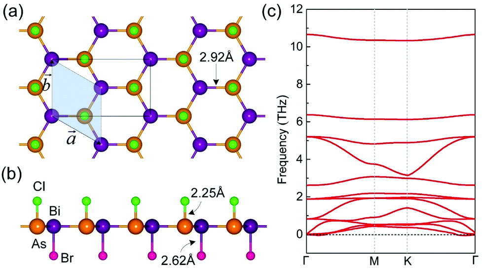 | ||
| Fig. 1 (a) Top and (b) side views for the atomic structure of BrBiAsCl ML. The shaded area with Bravais lattice vectors, a and b, represents its primitive cell. (c) Phonon dispersion curves of BrBiAsCl ML. | ||
Although the pristine β-BiAs ML has been confirmed to be a stable structure,19,22,41 it is indispensable to examine the feasibility of its Janus functionalization. Firstly, we calculate the formation energy of BrBiAsCl ML, defined as: Ef = (Et − Eβ-BiAs − μBr − μCl)/4. Here Et and Eβ-BiAs are the total energies of BrBiAsCl and β-BiAs MLs, respectively; μCl and μBr are the chemical potentials of Cl and Br atoms determined using the binding energy of gaseous Cl2 and Br2 molecules, respectively. The calculated Ef is −0.45 eV per atom, implying that the Janus functionalization of β-BiAs ML is an exothermal process. Therefore, BrBiAsCl ML should be superior to the pristine β-BiAs ML in terms of thermodynamic stability. The absence of imaginary frequency in the phonon dispersion (Fig. 1c) further indicates that BrBiAsCl is dynamically stable.
Inspired by the experimental advances in 2D V–V binary materials26–30 and Janus functionalized 2D materials,31,32 we speculate that the BrBiSbCl ML could be synthesized by two steps. First, one can directly produce β-BiAs monolayer using bottom-up approaches (e.g., chemical vapor deposition, wet chemical synthesis and molecular beam epitaxy), which have been employed to fabricate other V–V binary compounds, such as α-AsP and β-BiSb MLs,18 or indirectly obtain β-BiAs ML by mechanically exfoliating from the layered BiAs bulk crystals grown using the bottom-up approaches (the feasibility of mechanical exfoliation is shown in Fig. S3, ESI†). Then, one can further fabricate BrBiAsCl ML by the photohalogenation method, like in the case of Janus halogenated graphene.31
3.2 Intrinsic svc-DSM state
In the absence of SOC, the pristine β-BiAs ML is a non-magnetic semiconductor with a direct bandgap of 1.057 eV at the Γ point (see Fig. S4, ESI†). While the Janus functionalized β-BiAs ML is still a non-magnetic direct bandgap semiconductor (Fig. 2a), its bandgap is reduced to 0.772 eV and the location of the bandgap shifts from the Γ point to the K point. These changes can be explained by the strong coupling between the absorbed halogen atoms and the pz orbitals of Bi/As, which results in the pz orbitals being removed from the vicinity of the Fermi level, then the opposite hole and electron pockets with a smaller gap are formed at the K point, and a larger local gap is induced at the Γ point (see Fig. S4 for details, ESI†).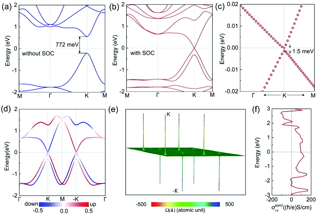 | ||
Fig. 2 The svc-DSM properties of BrBiAsCl ML: electronic band structures (a) without SOC and (b) with SOC. (c) Zoom plot for the linear dispersion bands in the vicinity of the Fermi level and the K point. (d) The four SOC bands in the vicinity of the Fermi level, together with the colour map of the Sz spin-texture. In the colour scale, blue represents spin-down states while red represents spin-up states. (e) Berry curvatures of BrBiAsCl ML in the kxy plane. (f) Intrinsic spin Hall conductivity  as a function of Fermi energy for BrBiAsCl ML. as a function of Fermi energy for BrBiAsCl ML. | ||
Interestingly, after the SOC effect is taken into account, the bulk bandgap at the K point is almost closed at the Fermi level with a tiny bandgap of 1.5 meV (see Fig. 2b and c), which is comparable with the proximity-induced bandgap (around 1 meV) of graphene placed on 2D MoS2.16 At temperatures higher than 17 K, such a tiny bandgap can be ignored. From the electronic band structure in Fig. 2b, one can see that the linear Dirac states (results from HSE06 calculations are given in Fig. S5, ESI†) are formed due to the giant spin-splitting resulting from the strong SOC interaction in heavy elements like Bi, As and Br and the breaking of inversion symmetry. The spin-splittings of the uppermost valence band (UVB, Δh) and the lowermost conduction band (LCB, Δe) are 0.306 eV and 1.272 eV, respectively, which are markedly larger than the values reported for SbAsH2 ML11 (Δh = 0.267 and Δe = 0.475 eV). For spintronic applications, such giant spin-splittings are beneficial to avoid spin-flip scattering.42,43 Moreover, the spin relaxation lifetime in BrBiAsCl is expected to be very long. It should be pointed out that although the current state of BrBiAsCl ML is conventionally referred to as Dirac state, the linear bands are spin non-degenerate, different from the case of the graphene-like Dirac state. In this regard, the low-energy fermions of BrBiAsCl ML are indeed Weyl fermions. To examine the transport behaviour of these Weyl fermions, their Fermi velocities vF are computed from a linear fitting: ℏvF ≈ dE(k)/dk. Along the K → M direction, the Fermi velocities of the hole and electron carriers are 5.44 × 10⁵ m s−1 and 5.31 × 10⁵ m s−1, respectively. While these velocities are smaller than that of graphene (9.42 × 10⁵ m s−1![[thin space (1/6-em)]](https://www.rsc.org/images/entities/char_2009.gif) 44), they are comparable to that of silicene (5.3 × 10⁵ m s−145).
44), they are comparable to that of silicene (5.3 × 10⁵ m s−145).
To examine whether the Dirac state of BrBiAsCl ML has the essential features of svc-DSM, we calculated its out-of-plane spin-texture and Berry curvature. As shown in Fig. 2d, the spin-texture of the Dirac bands along the k-path of Γ → K → M → (−K) → Γ for BrBiAsCl ML is presented with the projection of spin component Sz. The Dirac bands at the K and −K points have opposite out-of-plane spin moments, consistent with that of svc-DSM.11 On the basis of the construction of maximally localized Wannier functions, the Berry curvatures [Ωz(k)] of BrBiAsCl at the kz = 0 plane are calculated by the Kubo formula46–48 and presented in Fig. 2e. Owing to the breaking of inversion symmetry, the Berry curvatures of BrBiAsCl at K and −K exhibit prominent peaks but hold different signs, like the case of 2.3-SbAsH2 ML as a svc-DSM.11 Therefore, the low-energy massless fermions with the same energy can be distinguished or separated by their opposite out-of-plane spin moments as well as their opposite Berry curvatures. This is the precondition for the Dirac spin–valley Hall effect11 induced by an external in-plane electric field. To quantitatively examine the transverse anomalous motion, we calculate the intrinsic spin Hall conductivity (SHC) using the Wannier interpolation method.39,49 From Fig. 2f, one can see sizable spin Hall conductivity in a relatively large energy range. Particularly, from 0 to 0.6 eV relative to the Fermi level, the spin Hall conductivity remains almost constant [about 100 (ℏ/e) S cm−1] owing to the existence of spin–valley coupled linear bands, similar to the case of 2.3-SbAsH2.11
Because of the breaking of inversion symmetry, the Janus BrBiAsCl ML should have the Rashba effect, which combined with the spin–valley coupling (i.e., valley Zeeman interaction12) can produce a significant impact on the spin dynamics.12 To examine the Rashba effect, we calculated the in-plane spin-texture of BrBiAsCl ML. Fig. 3 presents the spin projected constant energy contour plots of the spin textures calculated in the kx–ky plane centered at the K point. Evidently, one can see the following typical characteristics of the Rashba SOC effect: (i) the pair of spin-splitting bands (i.e., the highest valence band corresponding to the large ring and the second highest valence band corresponding to the small ring) have opposite spin orientation for both Sx and Sy spin components. (ii) The in-plane spin moments (vector composition of Sx and Sy) at the two rings have opposite chirality – clockwise for the large ring and anticlockwise for the small ring, implying the existence of spin-momentum locking (i.e., the spin orientation perpendicular to the electron momentum).
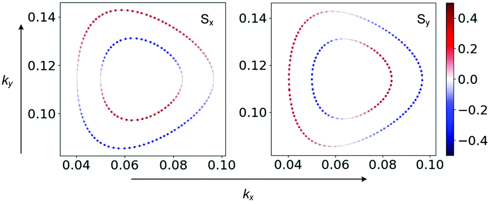 | ||
| Fig. 3 In-plane spin textures (Sx and Sy) calculated at the iso-energy surface of 0.6 eV below the Fermi level for BrBiAsCl ML. | ||
Another important characteristic of the svc-DSM state is that it locates at the phase boundary between 2D trivial and topological insulators.11 To this end, we further investigated the electronic and topological properties of BrBiAsCl ML under external strains. Fig. 4a displays the bulk bandgap as a function of biaxial tensile strain. With the strain increasing from −4% to 4%, the bandgap is reduced from 95 to 1.5 meV and then increases from 1.5 to 72 meV. Actually, the bandgap closing and reopening associated with the band inversion (see Fig. S6, ESI†) are reminiscent of a topological phase transition.50,51 Since the structure of BrBiAsCl ML is inversion-asymmetric, we calculated the Z2 topological invariant by tracing the evolution of 1D hybrid Wannier charge centers (WCCs).52,53Fig. 4b and c show the WCCs of −4% and 4% strained BrBiAsCl MLs, respectively. For an arbitrary horizontal reference line (e.g., WCC = 0.75), it crosses the evolution of WCC twice for the −4% strained BrBiAsCl ML and once for the 4% strained system. In other words, the compressively strained BrBiAsCl ML is a trivial insulator with Z2 = 0, while under tensile strain it transforms to a topological insulator with Z2 = 1. Further evidence can be seen from the edge states. For the trivial insulator under compressive strain (see Fig. 4d), the edge states of BrBiAsCl ML do not cross the Fermi level; they start from the valence band and then re-enter the valence band. In contrast, for the topological insulator under tensile strain (Fig. 4e), a pair of gapless non-trivial edge states traverse across the bulk gap, connecting the conduction and valence bands.
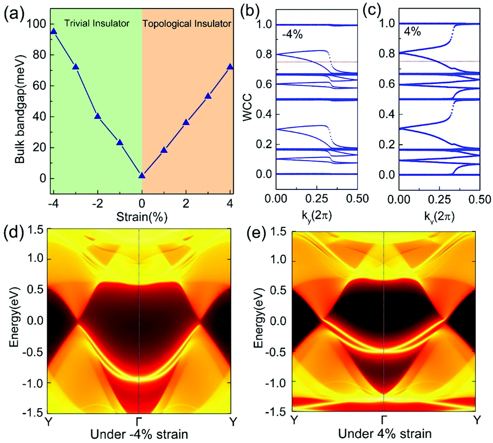 | ||
| Fig. 4 (a) The bulk bandgap of BrBiAsCl ML as a function of biaxial tensile strain under SOC. The evolution of Wannier charge centers (WCCs) along ky for (b) −4% and (c) 4% strained BrBiAsCl. The edge states of semi-infinite BrBiAsCl under (d) −4% and (e) 4% tensile strain. | ||
In the strain-free state, the bandgap is almost closed, which convincingly confirms that BrBiAsCl ML is a desirable intrinsic svc-DSM. The occurrence of the svc-DSM state could be attributed to a balance between the strength of the SOC and the built-in polarized electric field (EF) in the vertical direction of BrBiAsCl ML. Indeed, this corresponds to the topological phase transition between a 2D topological insulator and a trivial insulating state induced by the combination of a perpendicular EF (Δz) and intrinsic SOC (ΔSO), as previously found in buckled silicene.54 For Δz < ΔSO, the 2D structure is a topological insulator, while it becomes a band insulator when Δz > ΔSO. At the phase boundary, namely Δz = ΔSO (or Δz ≈ ΔSO), a linear Dirac state is formed with either a zero bandgap or a small bandgap of less than 25 meV (which is ignorable at room temperature; thus the linear band dispersion can be considered to be preserved) at the K or −K points. Therefore, to obtain the intrinsic svc-DSM, the following two conditions should be met: (i) the structure is inversion-asymmetric, which ensures that the Dirac cones will be spin non-degenerate under the SOC effect. (ii) In the perpendicular direction there exists built-in polarized EF, whose amplitude is appropriate so as to reach a balance with SOC (i.e., Δz = ΔSO or Δz ≈ ΔSO). In this work, the Janus structures XBiAsY (X/Y = F, Cl, Br and I, X ≠ Y) provide a basic model, which has both inversion asymmetry and built-in polarized EF. Based on such a Janus model, high-throughput computational searching with element substitution may be a powerful way to discover new svc-DSM in the future.
3.3 The svc-DSM state in substrate-supported BrBiAsCl ML
For device applications, it is desired to have the intrinsic svc-DSM state of BrBiAsCl ML preserved on a substrate. To address this, we consider insulating h-BN monolayer as the substrate, which has been commonly used for supporting various 2D materials.55,56 The possible BrBiAsCl@h-BN heterostructures are built by a 2 × 2 × 1 supercell of h-BN (a = b = 5.028 Å) and a primitive cell of BrBiAsCl (a = b = 5.057 Å), which match with each other very well with only 0.58% mismatch. Upon optimization with the inclusion of van der Waals (vdW) corrections within the DFT-D3 scheme,57 the structure with As–Cl bonds on the top of N atoms is confirmed as the most stable one, as illustrated in Fig. 5a and b. The interlayer distance between BrBiAsCl and the h-BN substrate is 3.15 Å, which is slightly smaller than that in the vdW heterostructure graphene@h-BN (3.22 Å).55 Hence, the interaction between BrBiAsCl ML and the h-BN substrate is a weak vdW interaction, which is further signified by the small interlayer binding energy of 0.075 eV per atom.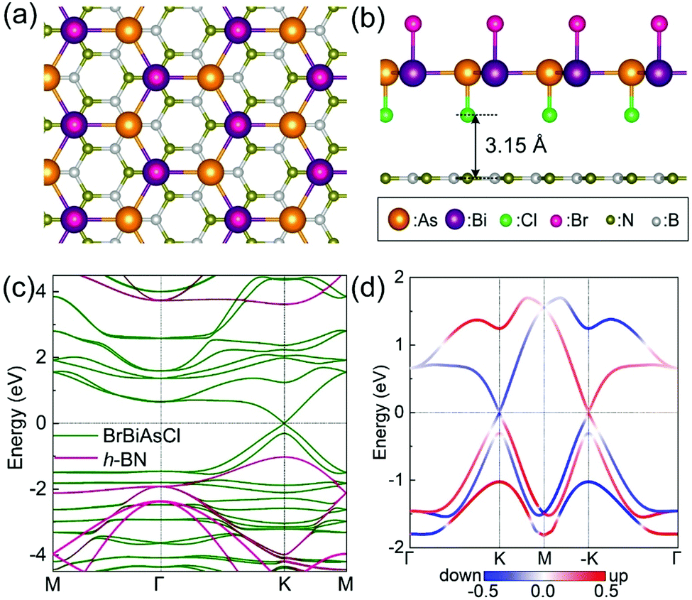 | ||
| Fig. 5 (a) Top and (b) side views of optimized BrBiAsCl@h-BN heterostructure with As–Cl bonds on the top of N atoms. (c) Band structures projected to h-BN and BrBiAsCl ML in the presence of SOC. (d) The bands of BrBiAsCl@h-BN in the vicinity of the Fermi level, together with the colour map of the Sz spin-texture. In the colour scale, blue represents spin-down states while red represents spin-up states. | ||
Benefiting from the vdW interaction, the svc-DSM state of BrBiAsCl ML is well preserved in the heterostructure. Fig. 5c shows the band structure of BrBiAsCl@h-BN with SOC. It can be found that the Dirac bands contributed by BrBiAsCl ML are almost identical to those of the free-standing BrBiAsCl ML. Remarkably, the sizable bandgap of 4.580 eV in the h-BN substrate guarantees that the spin-split Dirac bands of BrBiAsCl ML are very clear without being contaminated by the substrate states. Moreover, the essential feature of Dirac states at the K and −K points having opposite out-of-plane spin moments and in-plane spin-momentum locking (Fig. S7, ESI†) is also found in the BrBiAsCl@h-BN heterostructure (Fig. 5d). One can therefore conclude that h-BN ML is an ideal substrate for device implementation of intrinsic svc-DSM BrBiAsCl ML.
4. Conclusions
In summary, our first-principles computational screening of 24 possible ML structures of XBiAsY (X/Y = F, Cl, Br and I, X ≠ Y) unveiled the first intrinsic svc-DSM material, i.e., BrBiAsCl ML, which has Janus structure and satisfactory stability. After SOC is turned on, the bulk gap of 0.772 eV in BrBiAsCl ML is almost closed, forming a spin–valley-dependent Dirac state owing to the giant spin-splittings in UVB (0.306 eV) and LCB (1.272 eV). Our topological analysis showed that BrBiAsCl ML locates at the boundary between 2D trivial and topological insulators. Moreover, the intrinsic svc-DSM state of BrBiAsCl ML can be well preserved on the h-BN substrate. In view of the recent experimental progress with 2D group V–V binary materials and Janus functionalized 2D materials, the present theoretical findings will promote experimental studies of intrinsic svc-DSMs and exploit their fascinating properties in spintronics device applications.Conflicts of interest
There are no conflicts to declare.Acknowledgements
This work was supported by the National Natural Science Foundation of China (11964023, 11874097) and the 2020 Institutional Support Program for Youth Science and Technology Talents in Inner Mongolia Autonomous Region (NJYT-20-B02). The authors acknowledge the Cloud Computing Center of Lvliang “Tianhe-2” and the Super-computing Center of Dalian University of Technology for providing computational resources.References
- K. S. Novoselov, A. K. Geim, S. V. Morozov, D. Jiang, Y. Zhang, S. V. Dubonos, I. V. Grigorieva and A. A. Firsov, Science, 2004, 306, 666–669 CrossRef CAS.
- J. Wang, S. Deng, Z. Liu and Z. Liu, Natl. Sci. Rev., 2015, 2, 22–39 CrossRef CAS.
- S. Cahangirov, M. Topsakal, E. Akturk, H. Sahin and S. Ciraci, Phys. Rev. Lett., 2009, 102, 236804 CrossRef CAS.
- D. Malko, C. Neiss, F. Vines and A. Gorling, Phys. Rev. Lett., 2012, 108, 086804 CrossRef.
- Z. Wang, X. F. Zhou, X. Zhang, Q. Zhu, H. Dong, M. Zhao and A. R. Oganov, Nano Lett., 2015, 15, 6182–6186 CrossRef CAS.
- X. Wang, T. Li, Z. Cheng, X.-L. Wang and H. Chen, Appl. Phys. Rev., 2018, 5, 041103 Search PubMed.
- X.-F. Zhou, X. Dong, A. R. Oganov, Q. Zhu, Y. Tian and H.-T. Wang, Phys. Rev. Lett., 2014, 112, 085502 CrossRef.
- B. Feng, J. Zhang, S. Ito, M. Arita, C. Cheng, L. Chen, K. Wu, F. Komori, O. Sugino, K. Miyamoto, T. Okuda, S. Meng and I. Matsuda, Adv. Mater., 2018, 30, 1704025 CrossRef.
- S. Guan, Y. Liu, Z.-M. Yu, S.-S. Wang, Y. Yao and S. A. Yang, Phys. Rev. Mater., 2017, 1, 054003 CrossRef.
- S. M. Young and C. L. Kane, Phys. Rev. Lett., 2015, 115, 126803 CrossRef.
- Z. F. Liu, W. X. Feng, H. L. Xin, Y. L. Gao, P. F. Liu, Y. G. Yao, H. M. Weng and J. J. Zhao, Mater. Horiz., 2019, 6, 781–787 RSC.
- W. Savero Torres, J. F. Sierra, L. A. Benítez, F. Bonell, J. H. García, S. Roche and S. O. Valenzuela, MRS Bull., 2020, 45, 357–365 CrossRef.
- J. H. Garcia, M. Vila, A. W. Cummings and S. Roche, Chem. Soc. Rev., 2018, 47, 3359–3379 RSC.
- L. A. Benitez, W. Savero Torres, J. F. Sierra, M. Timmermans, J. H. Garcia, S. Roche, M. V. Costache and S. O. Valenzuela, Nat. Mater., 2020, 19, 170–175 CrossRef CAS.
- C. K. Safeer, J. Ingla-Aynes, F. Herling, J. H. Garcia, M. Vila, N. Ontoso, M. R. Calvo, S. Roche, L. E. Hueso and F. Casanova, Nano Lett., 2019, 19, 1074–1082 CrossRef CAS.
- M. Gmitra, D. Kochan, P. Högl and J. Fabian, Phys. Rev. B, 2016, 93, 155104 CrossRef.
- M. Gmitra and J. Fabian, Phys. Rev. B: Condens. Matter Mater. Phys., 2015, 92, 155403 CrossRef.
- S. Guo, Y. Zhang, Y. Ge, S. Zhang, H. Zeng and H. Zhang, Adv. Mater., 2019, 31, e1902352 CrossRef.
- H. Zhang and M. Chen, J. Mater. Chem. C, 2018, 6, 11694–11700 RSC.
- M. Xie, S. Zhang, B. Cai, Y. Huang, Y. Zou, B. Guo, Y. Gu and H. Zeng, Nano Energy, 2016, 28, 433–439 CrossRef CAS.
- J. Yuan, Y. Cai, L. Shen, Y. Xiao, J.-C. Ren, A. Wang, Y. P. Feng and X. Yan, Nano Energy, 2018, 52, 163–170 CrossRef CAS.
- C. Y. Wu, L. Sun, J. C. Han and H. R. Gong, J. Mater. Chem. C, 2020, 8, 581–590 RSC.
- S. Singh and A. H. Romero, Phys. Rev. B, 2017, 95, 165444 CrossRef.
- S. S. Li, W. X. Ji, P. Li, S. J. Hu, T. Zhou, C. W. Zhang and S. S. Yan, Sci. Rep., 2017, 7, 6126 CrossRef.
- Y. Nie, M. Rahman, D. Wang, C. Wang and G. Guo, Sci. Rep., 2015, 5, 17980 CrossRef CAS.
- E. P. Young, J. Park, T. Bai, C. Choi, R. H. DeBlock, M. Lange, S. Poust, J. Tice, C. Cheung, B. S. Dunn, M. S. Goorsky, V. Ozolinš, D. C. Streit and V. Gambin, ACS Appl. Nano Mater., 2018, 1, 4737–4745 CrossRef CAS.
- Y. Ueda, N. H. Duy Khang, K. Yao and P. N. Hai, Appl. Phys. Lett., 2017, 110, 062401 CrossRef.
- H. Gao, J. Niu, C. Zhang, Z. Peng and Z. Zhang, ACS Nano, 2018, 12, 3568–3577 CrossRef CAS.
- D. P. Shoemaker, T. C. Chasapis, D. Do, M. C. Francisco, D. Y. Chung, S. D. Mahanti, A. Llobet and M. G. Kanatzidis, Phys. Rev. B: Condens. Matter Mater. Phys., 2013, 87, 094201 CrossRef.
- B. Liu, M. Kopf, A. N. Abbas, X. Wang, Q. Guo, Y. Jia, F. Xia, R. Weihrich, F. Bachhuber, F. Pielnhofer, H. Wang, R. Dhall, S. B. Cronin, M. Ge, X. Fang, T. Nilges and C. Zhou, Adv. Mater., 2015, 27, 4423–4429 CrossRef CAS.
- L. Zhang, J. Yu, M. Yang, Q. Xie, H. Peng and Z. Liu, Nat. Commun., 2013, 4, 1443 CrossRef.
- S.-W. Ng, N. Noor and Z. Zheng, NPG Asia Mater., 2018, 10, 217–237 CrossRef CAS.
- G. Kresse and J. Furthmüller, Phys. Rev. B: Condens. Matter Mater. Phys., 1996, 54, 11169–11186 CrossRef CAS.
- G. Kresse and D. Joubert, Phys. Rev. B: Condens. Matter Mater. Phys., 1999, 59, 1758–1775 CrossRef CAS.
- J. P. Perdew, K. Burke and M. Ernzerhof, Phys. Rev. Lett., 1996, 77, 3865–3868 CrossRef CAS.
- H. J. Monkhorst and J. D. Pack, Phys. Rev. B: Solid State, 1976, 13, 5188–5192 CrossRef.
- A. Togo and I. Tanaka, Scr. Mater., 2015, 108, 1–5 CrossRef CAS.
- J. Heyd, G. E. Scuseria and M. Ernzerhof, J. Chem. Phys., 2003, 118, 8207–8215 CrossRef CAS.
- I. Souza, N. Marzari and D. Vanderbilt, Phys. Rev. B: Condens. Matter Mater. Phys., 2001, 65, 035109 CrossRef.
- Q. Wu, S. Zhang, H.-F. Song, M. Troyer and A. A. Soluyanov, Comput. Phys. Commun., 2018, 224, 405–416 CrossRef CAS.
- W.-Z. Xiao, G. Xiao, Q.-Y. Rong and L.-L. Wang, Mater. Res. Express, 2018, 5, 035903 CrossRef.
- S. Bandyopadhyay and M. Cahay, Appl. Phys. Lett., 2004, 85, 1433–1435 CrossRef CAS.
- Z. Y. Zhu, Y. C. Cheng and U. Schwingenschlögl, Phys. Rev. B: Condens. Matter Mater. Phys., 2011, 84, 153402 CrossRef.
- X. Zhang, A. Wang and M. Zhao, Carbon, 2015, 84, 1–8 CrossRef CAS.
- N. D. Drummond, V. Zólyomi and V. I. Fal'ko, Phys. Rev. B: Condens. Matter Mater. Phys., 2012, 85, 075423 CrossRef.
- D. J. Thouless, M. Kohmoto, M. P. Nightingale and M. den Nijs, Phys. Rev. Lett., 1982, 49, 405–408 CrossRef CAS.
- Y. Yao, L. Kleinman, A. H. MacDonald, J. Sinova, T. Jungwirth, D.-S. Wang, E. Wang and Q. Niu, Phys. Rev. Lett., 2004, 92, 037204 CrossRef.
- W. Feng, Y. Yao, W. Zhu, J. Zhou, W. Yao and D. Xiao, Phys. Rev. B: Condens. Matter Mater. Phys., 2012, 86, 165108 CrossRef.
- J. Qiao, J. Zhou, Z. Yuan and W. Zhao, Phys. Rev. B, 2018, 98, 214402 CrossRef CAS.
- S. Zhang, M. Xie, B. Cai, H. Zhang, Y. Ma, Z. Chen, Z. Zhu, Z. Hu and H. Zeng, Phys. Rev. B, 2016, 93, 245303 CrossRef.
- Y. Xu, B. Yan, H. J. Zhang, J. Wang, G. Xu, P. Tang, W. Duan and S. C. Zhang, Phys. Rev. Lett., 2013, 111, 136804 CrossRef.
- A. A. Soluyanov and D. Vanderbilt, Phys. Rev. B: Condens. Matter Mater. Phys., 2011, 83, 235401 CrossRef.
- A. A. Soluyanov and D. Vanderbilt, Phys. Rev. B: Condens. Matter Mater. Phys., 2011, 83, 035108 CrossRef.
- M. Tahir, A. Manchon, K. Sabeeh and U. Schwingenschlögl, Appl. Phys. Lett., 2013, 102, 162412 CrossRef.
- G. Giovannetti, P. A. Khomyakov, G. Brocks, P. J. Kelly and J. van den Brink, Phys. Rev. B: Condens. Matter Mater. Phys., 2007, 76, 073103 CrossRef.
- H. Liu, J. Gao and J. Zhao, J. Phys. Chem. C, 2013, 117, 10353–10359 CrossRef CAS.
- S. Grimme, J. Antony, S. Ehrlich and H. Krieg, J. Chem. Phys., 2010, 132, 154104 CrossRef.
Footnote |
| † Electronic supplementary information (ESI) available. See DOI: 10.1039/d0nh00466a |
| This journal is © The Royal Society of Chemistry 2021 |