
Long-lived charged states of single porphyrin-tape junctions under ambient conditions†
Edmund
Leary
 *abc,
Georg
Kastlunger
de,
Bart
Limburg
f,
Laura
Rincón-García
g,
Juan
Hurtado-Gallego
g,
M. Teresa
González
c,
Gabino Rubio
Bollinger
gh,
Nicolás
Agrait
cgh,
Simon J.
Higgins
a,
Harry L.
Anderson
*f,
Robert
Stadler
*i and
Richard J.
Nichols
*ab
*abc,
Georg
Kastlunger
de,
Bart
Limburg
f,
Laura
Rincón-García
g,
Juan
Hurtado-Gallego
g,
M. Teresa
González
c,
Gabino Rubio
Bollinger
gh,
Nicolás
Agrait
cgh,
Simon J.
Higgins
a,
Harry L.
Anderson
*f,
Robert
Stadler
*i and
Richard J.
Nichols
*ab
aDepartment of Chemistry, Donnan and Robert Robinson Laboratories, University of Liverpool, Liverpool L69 7ZD, UK. E-mail: R.J.Nichols@liverpool.ac.uk
bSurface Science Research Centre and Department of Chemistry, University of Liverpool, Oxford Street, Liverpool L69 3BX, UK
cFundación IMDEA Nanociencia, Calle Faraday 9, Campus Universitario de Cantoblanco, 28049 Madrid, Spain. E-mail: edmund.leary@imdea.org
dSchool of Engineering, Brown University, 02912 Providence (RI), USA
eDepartment of Physics, Technical University of Denmark (DTU), Fysikvej, 2800 Lyngby, Denmark
fDepartment of Chemistry, Chemistry Research Laboratory, Oxford University, Oxford OX1 3TA, UK. E-mail: harry.anderson@chem.oc.ac.uk
gDepartamento de Física de la Materia Condensada, Universidad Autónoma de Madrid, E-28049, Madrid, Spain
hIFIMAC and Instituto “Nicolás Cabrera”, Universidad Autónoma de Madrid, Madrid, E-28049, Spain
iInstitute for Theoretical Physics, TU Wien—Vienna University of Technology, Wiedner Hauptstrasse 8-10, A-1040 Vienna, Austria. E-mail: robert.stadler@tuwien.ac.at
First published on 19th October 2020
Abstract
The ability to control the charge state of individual molecules wired in two-terminal single-molecule junctions is a key challenge in molecular electronics, particularly in relation to the development of molecular memory and other computational componentry. Here we demonstrate that single porphyrin molecular junctions can be reversibly charged and discharged at elevated biases under ambient conditions due to the presence of a localised molecular eigenstate close to the Fermi edge of the electrodes. In particular, we can observe long-lived charge-states with lifetimes upwards of 1–10 seconds after returning to low bias and large changes in conductance, in excess of 100-fold at low bias. Our theoretical analysis finds charge-state lifetimes within the same time range as the experiments. The ambient operation demonstrates that special conditions such as low temperatures or ultra-high vacuum are not essential to observe hysteresis and stable charged molecular junctions.
New conceptsCharge transport in sub-5 nm 2-terminal molecular junctions nearly always operates in the coherent regime, where electrons traverse the molecular bridge in a single step. A few examples have shown fleeting charge localisation on the molecule when performed under ultra-high vacuum (UHV) conditions. There is a need, therefore, to understand whether charge localisation can be stabilised for longer timescales, and whether special conditions are required to form charged junctions such as UHV. Here, we answer both these questions. We have discovered charged single molecular junctions that are not only stable under ambient conditions, but survive on a record timescale of seconds. This represents a paradigm shift in the understanding of charge transport across redox-active molecules, since these previously unrecognised charged states greatly boost the junction conductance. We have discovered, using porphyrin-tapes, which can be considered as analogues of graphene nanoribbons, that charge-states can be stabilised for several seconds, reaching 10 s in certain cases. This has important implications for nanoscale science and molecular electronics since such long-lived charge states might offer future inspiration for memristor architectures or redox based molecular memories. |
Introduction
Porphyrins and their oligomers represent one of the most studied classes of molecular wires in single-molecule electronics. In such studies (oligo)-porphyrins are trapped between a pair of electrode contacts, typically gold, and their electrical properties are recorded by monitoring current flow through the junction at fixed bias voltage or by sweeping the bias to record I–V traces. For these measurements anchoring groups are required at each end, such as thiol1–3 or pyridyl4 moieties, although a broad series of other contacting groups have also been explored.5 Techniques typically used to wire individual molecules are the STM break junction method (STM-BJ),6 mechanically controllable break junctions (MCBJ)7,8 or a non-contact variant of the STM-BJ method called the I(s) technique.9,10 All techniques are capable of forming junctions down to the single molecule level and all require that large datasets are recorded and statistically analysed. In addition, longer polymeric porphyrin strands and bundles have been analysed within micro/nano fabricated devices.11,12Single-molecule electrical studies of (oligo)-porphyrin molecular wires have revealed their rich and attractive electrical properties. For example, they have been shown as efficient conduits of electrical charge at both shorter and longer lengths, and are found to conduct by phase-coherent tunnelling up to lengths of at least 5 nm at low and moderate bias voltages.4,13–15 Low conductance-attenuation with length (represented by the so called β-value) has been observed in both the butadiyne-linked1 and ethyne-linked13 series of monomer, dimer and trimer porphyrin wires. More recently, the bias voltage dependence of such β-values has been analysed in detail.14 For the butadiyne-linked compounds, the low-bias β-value of 2 nm−1 reduced to less than 1 nm−1 at 0.9 V. Furthermore, in the same study it was found that β can become negative at higher bias for the fused oligomers, even within a phase coherent tunnelling regime. In other words, molecular wires can exhibit increasing conductance with length, a feature that contrasts with both metallic chains and ohmic conductors and has not been previously observed for other single-molecular bridges. Porphyrin monomers and oligomers have featured in a host of other single-molecule electrical studies. This includes studies of the influence of inter-ring connectivity on the conductance of oligo-porphyrins,16 the effect of pendant anchoring group positioning with respect to a porphyrin monomer,17,18 mechanically induced atropisomerisation,19 the influence of binding geometry,19–21 two-state switching arising from conformational changes,22 the effect of changing the coordinating metal,23 bias-modulated hybridisation (depending on the backbone)24 and highly conductive junctions through coordination at the axial metal centres.25
Oligo-porphyrins have rich and tuneable electronic and redox properties,26 which have been exploited in molecular dyads,27,28 with potential applications including dye-sensitised solar cells and photocatalysis.29 Extensive investigations have been undertaken for the photochemical/photophysical properties of porphyrin-containing dyads. These have shown, for example, enhancements of the photocurrent generation using longer porphyrin oligomers and the ability to form long-lived charge-separated states with high quantum yields.30,31 On the other hand, the redox properties and charging of porphyrin wires have barely been exploited in direct single-molecule electrical platforms. An exception here is the study of porphyrin/fullerene single-molecule wires by the Lindsay group, where photo-induced redox-charging of a porphyrin following intra-molecular charge transfer to a fullerene acceptor was implicated in the appearance of high-conductance and long-lived excited states observed in STM-BJs.32 Given the status of oligo-porphyrins as archetypical single-molecule wires and their documented redox properties they are good candidates for fundamental investigations of the influence of charging phenomena on molecular conductance.
Although switching between redox states of molecular wires can be achieved under electrochemical potential control,8,33 or in solid-state gated 3-terminal molecular junctions,34–37 it is also recognised that charging can be induced by the bias voltage in 2-terminal molecular junctions. In this latter case charging phenomena can lead to pronounced nonlinear current-bias voltage characteristics accompanied by marked hysteresis.38 Examples of such behaviour have been found in several organometallic compounds39–42 and 1,3-azulene derivatives.38,43 Such studies were performed at low temperatures (50 K) under ultra-high vacuum (UHV) in MCBJ configurations with gold electrodes. Bias voltage sweeping led to voltage-induced charging of localised molecular orbitals (MOs) which are weakly coupled to the enclosing electrodes. This creates a charge-hopping channel (so called “slow channel”) alongside a “fast” coherent one which is usually associated with a fully delocalised frontier molecular orbital. The slow channel is only activated at appropriately high bias voltages and has the ability to alter the alignment between the strongly coupled molecular states and the Fermi level in the electrodes. This dual channel mechanism accounts for both the conductance boost and switching, as well as hysteresis in the forward and reverse I–V curves. The appearance and relative longevity of the hysteresis during bias voltage sweeps is explained by the weak coupling of the particular MOs. A first theoretical model for the described mechanism was proposed by Migliore and Nitzan, who applied a combination of Marcus and Landauer–Büttiker theory, describing electron transfer rates in the slow channel and resonant tunnelling in the fast channel, respectively.39 Charging was also discussed as a factor in the conductance of oligo(thiophene 1,1-dioxide)s when subjected to a high bias voltage leading here to negative differential resistance (NDR).44
Despite the fact that bias-voltage charging phenomena have been characterised in two-terminal single-molecule junctions at ultra-low temperatures in UHV, it remains far from clear whether such charging could be achieved with sufficient longevity in single-molecule junctions under ambient conditions. Demonstrating and exploiting this hysteresis in two-terminal single-molecule junctions will have important implications for molecular electronics. First, future devices operating under ambient conditions would have greater potential applications than low temperatures ones. Second, two-terminal molecular devices would be more achievable than gated 3-terminal ones. Third, hysteretic I–V behaviour and long-lived charged junction states might offer future inspiration for memristor architectures or redox based molecular memories.45,46 Nevertheless, although such future devices seem distant, STM break junction studies provide a strong platform for fundamental investigations of room-temperature conduction mechanisms in oligo-porphyrins and the impact of bias voltage-induced charging phenomena. From the perspective of obtaining charged states, fused-porphyrin tapes represent ideal candidates thanks to their ultra-low HOMO–LUMO gaps and the fact they can be synthesised with groups that provide weak to moderate coupling, as is the case with the phenylacetylene units used here. This forms the basis for this study in which we will show that edge-fused porphyrins can be made to switch between a low (uncharged) and high (charged) conductance state and remain in this high state for seconds at room temperature. Our theoretical treatment finds similarly long-lived charge states which last on average for 4–6 seconds.
Results and discussion
Fig. 1 shows the structures of compounds P1 (monomer), fP2 and fP3 (fused porphyrin dimer and trimer, respectively) which were synthesised as described previously.14 Such compounds have obvious parallels with graphene nanoribbons (GNR).47 The electrochemical and optical HOMO–LUMO gap decreases substantially along the series (reaching less than 1 eV for the trimer). The thiophenylacetylene linker groups provide a relatively weak coupling of the central porphyrin unit to the electrodes while the presence of bulky side groups prevents significant aggregation and supresses potential Au–π interactions. In this work, we focus primarily on the fused trimer fP3, which has the lowest HOMO–LUMO gap of the three, and also the P1 which primarily serves as a comparison/control. The results for fP2 are given in the ESI.† | ||
Fig. 1 Structures of the compounds investigated. P1 (monomer), fP2 (fused-porphyrin dimer) and fP3 (fused-porphyrin trimer). R1![[double bond, length as m-dash]](https://www.rsc.org/images/entities/char_e001.gif) OC8H17, R2Si(C6H13)3. OC8H17, R2Si(C6H13)3. | ||
The voltage-dependent transport behaviour of single porphyrin junctions was studied using a home-built scanning tunnelling microscope (STM), employing the break-junction (BJ) technique operating under ambient conditions. Full details of the procedure can be found in the ESI,† Section S1. Briefly, the STM tip is driven in and out of contact with the surface, during which time the current is recorded as a function of z-piezo movement. When a molecule becomes trapped, producing characteristic current-distance plateaus (see ESI,† Section S1.4 for examples), we pause the piezo motion at regular intervals and carry out bias sweeps to record current–voltage (I–V) traces, which are plotted as log(G/G0) − V, where G = I/V and G0 = 77.5 μS. The voltage is first ramped to the maximum positive value, from where we perform an ‘out and back’ bias sweep during each piezo pause, starting and ending the ramp at the maximum positive voltage (+V to −V, coloured black and −V to +V, coloured red; for examples see ESI,† Section S1.4). After each out and back sweep, the piezo is moved to the next position, and the process repeated until the junction breaks down. Between I–V measurements the current is recorded at a bias of 0.2 V in order to obtain full information about the junction during the stretching and construct a complete G–z trace. Stretching the junction allows us to explore different coupling strengths of the molecule to the electrodes, which is important as the charge-state lifetime is dependent on this parameter.
Charging the molecule
In the following we will show that increasing the upper limit of the bias voltage sweep changes the average shape of the G–V curves. Fig. 2a shows the mean log(G/G0) − V curves for fP3 measured by either ramping the voltage between ±0.8 V (black line), ±1.0 V (red line) or ±1.2 V (blue line). The speed of retraction in this series of experiments was 2.6 nm s−1 and the voltage ramp was performed at a rate of 0.7 V s−1. When the voltage is restricted to ±0.8 V, the average shape of the log(G/G0) − V curves generally resembles an ‘open-U’. Increasing the voltage window does not, however, simply extend the same mean log(G/G0) − V curve further. Instead, opening the bias range to ±1.0 V results in a change to the mean curve, which now appears more ‘V-shaped’, particularly at low bias (see Fig. S1c (ESI†) for individual examples). The mean shape changes further still when extending the range to ±1.2 V, becoming more of an ‘open-V’ (see Fig. S1d for individual examples, ESI†). For some junctions, the mean G–V curve is a good representation of the shape of the individual traces, such as in Fig. 2b and c, where the black line is the mean log(G/G0) − V curve for all the individual traces recorded on a single junction, which is superimposed on the 2D histogram of all traces. On the other hand, in some junctions, the shape of individual traces can vary significantly. Fig. 2d shows such an example in which both ‘U’-shaped and much flatter traces are present. In this case, the mean trace is not a good representation of any of the individual traces. In other examples, traces can display a steep rise followed by a levelling-off above a certain voltage (see Fig. S1b, ESI†). When this happens, it indicates that one of the molecular levels has become aligned with the Fermi level.48,49 Others show only a steep rise (Fig. S1a, ESI†). Further examples of the individual generic shapes we find are shown in Fig. S1 (ESI†).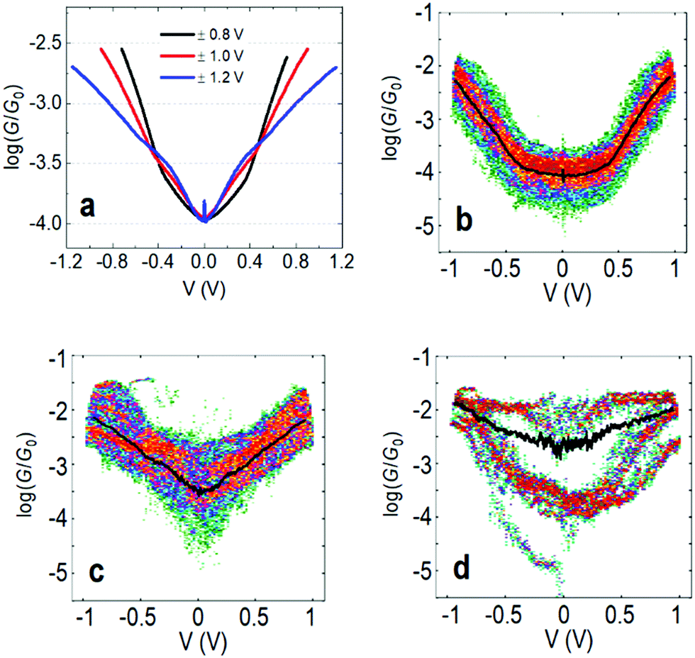 | ||
| Fig. 2 (a) Mean log(G/G0) − V traces for fP3 using different bias voltage windows. (b–d) 2D histograms of the log(G/G0) − V behavior for individual junctions for the bias range ±1.0 V. All G–V curves recorded in each junction are represented by the 2D histograms. The solid black lines are the mean conductance curves. Corresponding G–z traces are shown in Fig. S13 (ESI†). Panel (b) shows mean log(G/G0) − V traces with a characteristic ‘U’-shape, while (c) shows mean traces with a ‘V’-shape. (d) A junction which switches between ‘U’-shaped and much flatter traces, indicative of molecular charging. | ||
The change in the average curve suggests a change in transport mechanism at higher bias voltage. It is clear, however, from Fig. 2d that looking at averaged traces hides important information about junction behaviour. The average trace here (black line) is not truly representative of any of the individual traces in this junction (represented by the 2D-plot of the data).
To understand this behaviour in more detail we carried out an unsupervised k-means clustering subdivision of the G–V traces (for details please see ref. 50). Such methodologies have been applied recently in single molecule conductance studies to separate G–z traces.50–52A priori, it is unclear how many blind subdivisions to request. From the mean G–V traces shown in Fig. 2a it seems clear that as the bias voltage window is increased the percentage of ‘U’-shaped traces diminishes. As such, we can divide the traces into two groups, those with predominantly ‘U’-shape and those with other shapes. A visual inspection of the data, however, shows that the absolute shape of individual traces can vary significantly. To carry out the division, therefore, we initially divided traces into as many groups as necessary such that the general shape in each group is similar. We then combined all groups of predominantly ‘U’-shape into a single group, and combined the rest into a further group (Fig. S15, ESI†). The percentage of each group for each voltage window are represented in Fig. 3 using a bar chart. Here we see that the ratio of ‘U’-shaped traces to other shapes is initially high when the bias voltage window is ±0.8 V, but steadily decreases as the window is expanded. At ±1.2 V, there are virtually no clearly ‘U’-shaped traces. A visual inspection of the individual traces at ±1.2 V shows that there are a handful of ‘U’-shaped traces, but not enough to result in a distinct group during the clustering process.
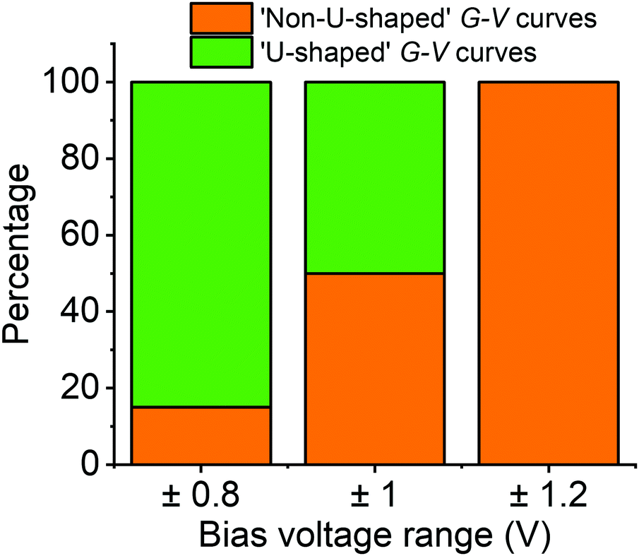 | ||
Fig. 3 Percentage of G–V traces with ‘U’ and non-‘U’ shapes within the various voltage ranges studied for fP3. There is an uncertainty of a few percent for each range. ‘U’-shaped traces are associated with the neutral state of the molecule. Non-‘U’-shaped traces are associated with the molecular charging. The total number of G–V traces recorded at each voltage were: 12![[thin space (1/6-em)]](https://www.rsc.org/images/entities/char_2009.gif) 673 (±0.8 V), 7084 (±1.0 V) and 6567 (±1.2 V). 673 (±0.8 V), 7084 (±1.0 V) and 6567 (±1.2 V). | ||
We carried out the same clustering analysis for the monomer P1 which showed far fewer non-‘U’-shaped curves when exploring the same ±1.2 V range. To be precise, out of over 6000 G–V curves recorded on P1, we found only about 1% could be described as non-‘U’-shaped (see Fig. S22, ESI†). In general, the G–V traces are much flatter than for fP3, tending not to level-off at high voltage, and the vast majority do not show any hysteresis (see Fig. S2–S5 for examples, ESI†). The behaviour described for fP3 is therefore very different in comparison to P1.
The behaviour of the mean G–V traces for fP3 combined with the clustering analysis suggests that the Fermi level alignment of the molecular tunnelling channels might be significantly altered when exploring higher bias voltages for this molecule. To gain further insight, we now focus on the behaviour of individual junctions which exemplify the G–V behaviour. Fig. 4a shows a single molecule junction of fP3 in which G–V curves were recorded between ±1.0 V along its entire stretching length as the tip is moved away from the substrate. Initially, the G–V curves can be described as ‘U’-shaped but with some levelling at high bias, and fully reversible (Fig. 4b, recorded at a distance as shown by the orange highlighted region in the inset to Fig. 4a corresponding to a real electrode gap of 1.3–1.4 nm allowing for the initial jump-out-of-contact or “snapback”). This shape is indicative of off-resonant transport at low-bias. A sudden change is seen, however, in the subsequent curves (Fig. 4c) obtained at slightly larger z-extension in the red highlighted region in the inset of Fig. 4a. The reversible behaviour is lost, and the traces start to behave differently. As seen in Fig. 4c, when the bias is swept from 0 V to −1 V (black trace), the conductance initially increases in a manner similar to before, but jumps to a higher level at about −0.6 V, continuing to rise only slightly thereafter. In the return (red) trace, the conductance initially follows the previous (black) trace, but rather than decreasing to below log(G/G0) = −4, it remains above log(G/G0) = −3 for the entire return sweep. In the following bias sweeps (Fig. 4d) the conductance switches back and forth between the high and low states. The junction continues with this switching behaviour as it is stretched further (G–V curves not shown here) until rupture at circa 2.2 nm in Fig. 4a (2.6–2.8 nm real electrode separation, which is about 1 nm less than the full molecular length). In this particular junction, the longest time the molecule remained in the high conductance state was 0.7 s from panel (c) to (d), with a high:low conductance ratio of about a factor 50 around zero-bias. This behaviour is consistent with that described by Schwarz et al.41,43 in which a localised MO on the molecule becomes charged resulting in closer alignment between the HOMO/LUMO and the Fermi level. We therefore ascribe the sudden jump observed in the black trace of Fig. 4c to the spontaneous charging of the junction, with subsequent jumps corresponding to either charging (jump up) or discharging (jump down).
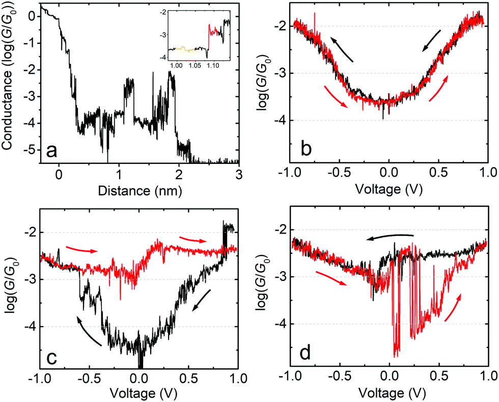 | ||
| Fig. 4 Example of the charging and discharging of a single fP3 molecule junction. (a) Full conductance plateau. The inset shows a zoom of the region where the junction first becomes charged. (b) G–V curves recorded before charging occurs (recorded during the orange highlighted section in the inset to (a)). The black trace (starting at +1.0 V) precedes the red trace. Arrows indicate the corresponding voltage-sweep direction. (c and d) G–V curves recorded during the red highlighted section in the inset of (a). The maximum time the molecule remains in the high conductance charged state is 0.7 s between (c) and (d). The zero-bias high-low conductance ratio is about a factor 50. | ||
For fP2 we have measured the bias-voltage dependence for the ranges ±0.8 and ±1.0 V, and the clustering analysis for these is shown in Fig. S19–S21 (ESI†). For the ±0.8 V window all G–V curves could be classed as ‘U’-shaped and thus showing no evidence of charging. For a window of ±1.0 V, however, 8% were classed as non-‘U’-shaped and associated with charging behaviour. This demonstrates that for the same bias voltage window, fP2 can be charged as can fP3, but with a lower probability.
Measuring long-lifetime charged junctions
In order to measure the charged state lifetime more accurately, we designed a further set of experiments based on a pump–probe methodology. The idea was to begin at low bias and quickly ramp the voltage up to a high value and then back again and record the current as a function of time. We decided to maintain a slow speed of electrode separation between bias sweeps, however, as at room temperature it is difficult to control the intrinsic drift suffered by the microscope (which is approximately 0.05–0.1 nm s−1 in the XY plane). Retracting the tip at 0.26 nm s−1 avoids the possibility that the drift will cause the junction to close, potentially sandwiching the molecule, and does not significantly limit the level of accuracy achievable under these conditions. We began the ramp at low bias (−0.1 V) and ramped the voltage to +1.0 V and back. Fig. 5a shows representative behaviour for junctions showing charging phenomena. In the first example (G–z trace shown in Fig. 5a and the corresponding G–V curves in Fig. 5b) we find the junction initially in the low conductance state between log(G/G0) = −4 and −5. At a distance of 1 nm (1.4 nm actual separation) the voltage was ramped to 1.0 V (black trace in Fig. 5b) and we observed a pronounced jump up in conductance between 0.6 V and 0.7 V. Upon returning to low bias (red trace) the conductance remains close to log(G/G0) = −2, which persists during the slow retraction as seen in Fig. 5a. Another G–V curve (blue curve, Fig. 5b) confirmed that after several seconds the junction still remained in the charged state, closely resembling the previous trace. Further retraction caused the conductance to decay and ultimately for the junction to rupture at a separation of about 2.5 nm (ca. 3 nm absolute separation, which is close to the maximum theoretical junction length of 4 nm). In this junction we determine that the molecule remained in the high-conductance charged state for 6–8 s. Potentially this time could be greater, but it is possibly limited by the movement of the tip and we speculate that the high conductance state could have survived even longer if all motion had been eliminated, which is very difficult under ambient conditions. To the best of our knowledge, we do not know of any other example of such a long-lived transient charged-state under these conditions.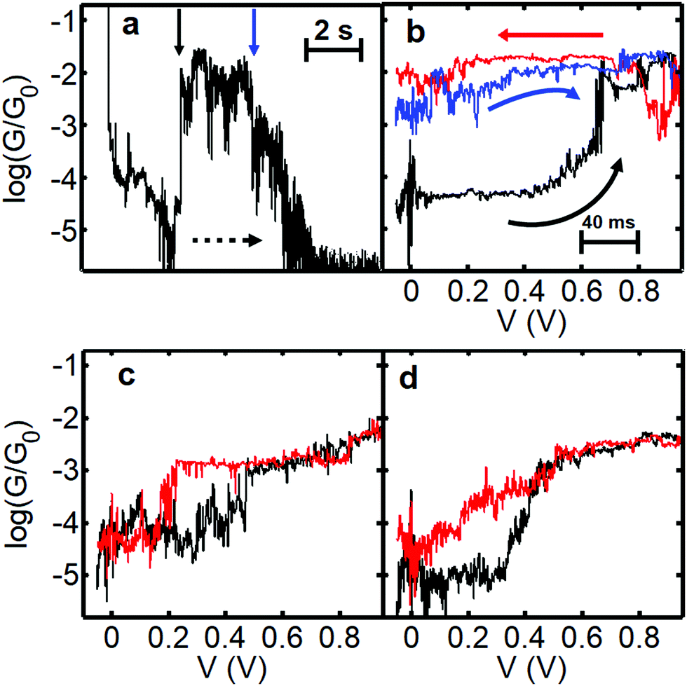 | ||
| Fig. 5 Data illustrating charging and hysteretic G–V behaviour for fP3. Panel (a) shows a slow retraction trace displaying log(G/G0) versus displacement and time (rate = 0.26 nm s−1, bias voltage = 0.2 V). The dashed arrow indicates the direction of junction evolution. To obtain the total charge-state time, the time spent performing the G–V curve must be added. The respective bias sweeps are shown in panel (b). The bias is swept from −0.1 V to 1.0 V and back. The initial (black) and return (red) trace in (b) was recorded at a distance marked by the vertical black arrow (the actual displacement is 1.4–1.6 nm considering the initial snapback). The blue trace in (b) was recorded at the position of the blue arrow (2.3 nm tip-surface separation). Panels (c) and (d) show examples of G–V traces where the junction charges and discharges during the course of the bias sweep. In (c) the charging appears discreet whereas in (d) it is a more gradual process. The corresponding full G–z traces are shown in Fig. S14 (ESI†). | ||
When hysteresis is seen, the most common outcome is for the junction to return to the low conductance state before the end of the bias sweep (i.e. the molecule charges and discharges during the same voltage sweep). The example shown in Fig. 5c shows a relatively abrupt jump up in conductance at 0.5 V (black trace) and down again at 0.2 V (red trace) within the same out and back sweep. Here the time in the high conductance (charged) state is about 1 s. In Fig. 5d a more gradual conductance increase is seen in the black ramp before the trace ultimately levels off. In the return (red) trace the conductance drops to almost the original value of log(G/G0) = −5 at zero bias, but clearly follows a different trajectory, with the trace more like an open-‘V’. Here it was not possible to discern a clear point at which the molecule discharges. Instead, it is possible that many sequential charging and discharging events took place during the sweep, leading to an average curve between neutral and charged states (it is known that the charging rate depends strongly on the coupling to the electrodes41). If so, this implies that in cases such as this the charging/discharging takes place on timescales smaller than the time interval between points in the voltage sweep (which is about 2 ms). The red trace in Fig. 5d is typical of the general shape found when applying a bias window of ±1.2 V in the previous experiments (see Fig. S17, ESI†). This could indicate that the typical lifetime under these conditions is relatively low, and the longer-lived states are thus less common.
Other studies, using different methods, have found evidence that charge states can persist for similar timescales as found in this work. Long-lived charge-separated states of a photo-illuminated porphyrin-fullerene dyad were observed in single-molecule junctions formed between gold and ITO electrodes.53 We also note that long-lived charged states, with lifetimes on the order of seconds, have been observed in plasmon-excited molecular tunnel junctions as determined by Surface Enhanced Raman Spectroscopy (SERS).54
Conductance switching during the stretching of a single molecule junction is found to some degree in virtually all junctions, regardless of the compound being studied. This is normally attributed to changes in the binding between the anchor groups and the electrodes, where the absolute conductance depends on the coupling strength and produces no correlation with the shape of the G–V trace. Whilst we fully expect such processes to occur here, leading to conductance jumps, these events cannot explain the hysteretic G–V behaviour observed in tandem with a conductance jump. As a way of showing this, in the single level model (SLM) of electron transport, the degree of curvature of a G–V curve can be shown to depend primarily on the relative position of the frontier orbitals and the Fermi level.55 If only the coupling was changing, then a higher conductance across the entire voltage range should be seen. In Fig. S28 (ESI†) we show the results of a SLM analysis which shows that changing the coupling by changing Γ (the single level broadening term) shifts the calculated G–V traces along the vertical (conductance) axis and does not significantly change their shape. Such behaviour is not what we observe in the examples of Fig. 4 and 5 in which all the out-and-back traces have essentially the same conductance at high bias, differing only at low bias. On the other hand, if the frontier orbital-Fermi level difference changes (represented by ε0 in the SLM) this produces an effect consistent with the described behaviour (see Fig. S29, ESI†). Such a realignment is expected when the molecular charge state changes.
Assuming that transport takes place via coherent tunnelling within the HOMO–LUMO gap for ‘U’-shaped curves, we can determine the level alignment by differentiating the I–V curves and determining the peak in the dI/dV. We have done this for the traces recorded on the junction shown in Fig. 4b (by averaging several traces, see Fig. S15 (ESI†) for the final dI/dV curve) finding the peak lies at close to ±0.8 V. For a molecular junction wired to two electrodes, then assuming symmetric couplings, the position of the level is given by half the voltage (at positive or negative bias) at which the peak is found (Vpeak/2). This, therefore, gives an energy offset of 0.4 eV between EF and the frontier molecular orbital. In the following section we will show that charging of the molecule reasonably explains the observed behaviour, which causes a frontier orbital to align closely with the Fermi level. This can logically account for the hysteresis in which the forward and reverse G–V curves have a similar conductance at high bias, but a different conductance at low bias.
Theory section
In order to obtain the transmission functions and the spatial localisation patterns as well as eigenenergies of the relevant MOs close to the Fermi level for P1, fP2 and fP3 we have performed NEGF-DFT calculations. In the following section we will focus on fP3, while the detailed results for the P1 and fP2 junctions are given in the ESI.† As shown in Fig. 6, we find that the conductance of fP3 is determined by the frontier orbitals, which result in broad peaks, while the HOMO−1 is rather decoupled from the electrodes with almost no localisation on the anchor groups. We note that the HOMO−1 is derived from the a1u orbitals of the porphyrin monomers, having nodes at the meso positions and as such does not couple to the anchor groups. The HOMO is derived from the a2u orbitals which have large coefficients at the meso positions and thus couples strongly to the electrodes. Thus, the resulting peak derived from the HOMO−1 in the transmission function can only be made visible when the energy scale is highly enlarged. Such a decoupled MO close to the Fermi level allows for a charged state on the molecule with measurable lifetimes as the probability of a charge to move on to the next electrode is quadratically proportional to the coupling. We also assessed the potential role of the Zn ion in the hopping process by looking at the density of states projected onto the Zn. The results (shown in Section S2.5 of the ESI†) reveal that the Zn states are located far away in energy from the Fermi level and thus do not play any role in the transport.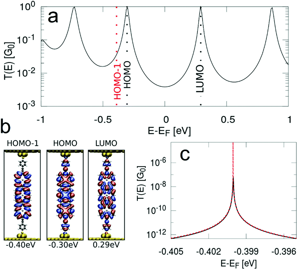 | ||
| Fig. 6 (a) Transmission function, (b) spatial localisation of the frontier MOs and (c) the transmission peak of the HOMO−1 on an enlarged energy scale as calculated for the junction with molecule fP3 from NEGF-DFT. | ||
For such cases, a two-channel model has been proposed,39,41 in which the conductance is defined by a “fast” coherent tunnelling channel through delocalised MOs and a “slow” hopping channel through a localised MO, which leads to conductance switching (and hysteresis) between a neutral and a charged state. We simulate G–V curves incorporating conductance switching by using this stochastic two-channel model39,41 which combines NEGF-DFT to describe the coherent tunnelling for the “fast” channel and DFT-based hopping rates according to Marcus theory14 for the “slow” channel for molecule fP3 (Fig. 7). The hopping path leads to a transient charging of the compound which results from a competition between the redox process and the experimental sweeping rate.38,39,41–43
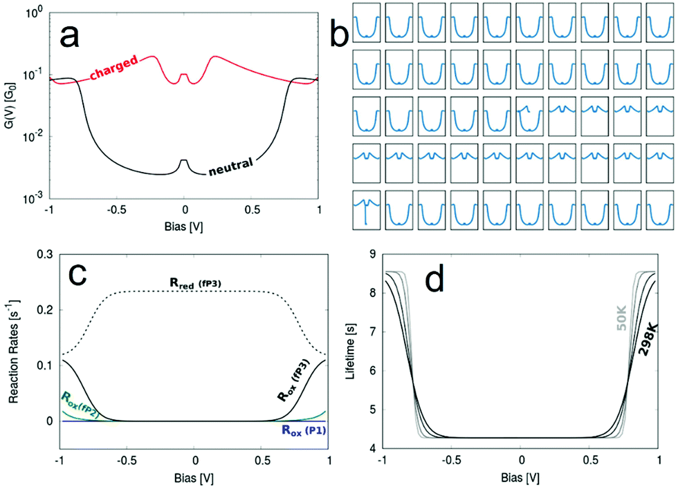 | ||
| Fig. 7 (a) Bias dependent G curves for the neutral and charged state. (b) A representative run simulating the switching of G between the two states. The x-axes represent voltage and the y-axes conductance. (c) Calculated reaction rates for the oxidation and reduction via filling/emptying of the molecular HOMO−1. (d) The charged state lifetime and its temperature dependence (bottom right) for the fP3 junction. The parameters used are εHOMO−1 = −0.40 eV − EF, Γ = 3.5 × 10⁻⁹ eV, λ = 0.01 eV and their source is described in the ESI.† | ||
Pronounced switching between the uncharged and charged state of the molecule can be seen in Fig. 7b, where Fig. 7a shows the two “pure” G–V curves for the two states. The charged G–V curve is derived from a transmission function obtained from a DFT calculation where a positive charge has been localised on the molecular bridge using the Delta SCF technique.56 The relevant quantities determined from fitting a Lorentzian distribution to the weak coupling transmission peak of the HOMO−1 are given in Table 1 with further details described in the ESI.†
| P1 | fP2 | fP3 | |
|---|---|---|---|
| ε HOMO−1 − Ef [eV] | −0.96 | −0.49 | −0.40 |
| Coupling strength Γ [eV] | 6.5 × 10⁻⁹ | 1.3 × 10⁻⁸ | 3.5 × 10⁻⁹ |
The switching does not happen in every simulated run, but in 7 out of the 16 runs. The lifetime varies significantly between different runs, which is a consequence of the stochastic model used for the simulation, described in more detail elsewhere42 and the ESI.† However, in general the lifetime of the switching is remarkably long. In one of our simulation runs the switching was stable for about 9 s. This is, however, an extreme example and on average the switching is stable for about 4–6 s.
In Fig. 7c we show the oxidation rate Rox for molecules P1, fP2 and fP3, which defines the rate for the corresponding junction to be charged depending on the bias. Only for fP3 does this rate becomes significantly high within the experimentally swept bias window of ±1.0 V because only for this molecule is the HOMO−1 close enough to the Fermi level. This explains why charging is observed for fP3 in a significant proportion of the measurements. For fP2 charging is still possible, but much less likely, hence the lower occurrence experimentally of non-‘U’-shaped G–V curves (Fig. S21, ESI†).
For a more rigorous way of defining the mean lifetime of the charged state the actual rate of the electron-transfer reactions inducing the switching can be used. These reaction rates are calculated from DFT40 and the mean value of the lifetime can be estimated as τ = Rred−1(V). The reduction rate Rred is chosen since it corresponds to the rate of discharging the charged state again. Since Rred is a function of the applied bias, so too is τ, as can be seen in Fig. 7d where the temperature dependence of τ(V) is also illustrated. We determine τ = 4.28 s at low applied biases, while at high biases close to 1 V the lifetime increases to 8.56 s. Between the two extremes (as defined by magnitude of the electronic coupling) the lifetime varies smoothly and the shape of τ(V) is a function of both the temperature and the reorganisation energy.
The clustering analysis of the G–V curves into ‘U’ and non-‘U’ shaped sets allows us to set limits to the average location of the frontier molecular orbitals. Given that we find the percentage of non-‘U’-shaped traces (associated with charging) increases from about 15% within a bias window of ±0.8 V to close to 100% within a bias window of ±1.2 V (Fig. 3), we can confidently place the charging level closer than 0.6 eV from EF (taking the bias voltage on average to drop linearly to 50% at the centre of the molecular junction). Bearing in mind that the electrochemically measured HOMO–LUMO gap of fP3 is 0.78 eV and the optical gap is 0.89 eV, then in the limiting case that there is no significant change in the gap upon binding to gold, and that the Fermi level sits close to the centre of the gap, the frontier orbital-EF difference should be between 0.40–0.45 eV (n.b. it could be smaller than this due to image charge effects57 or if there is a shift in EF). The position of the frontier molecular orbital found from the data in Fig. 4b was 0.4 eV (determined from the peak of the dI/dV curve, Fig. S15, ESI†), and is representative of the average position. Thus, the energy difference as determined from the dI/dV curve agrees well with the spectroscopic gap. This therefore allows us to determine the energy difference between the frontier MO (the HOMO in the case of fP3 according to our theory) and the charging orbital (the HOMO−1) which is thus no more than 0.2 eV (i.e. 0.6 eV–0.4 eV). This energy difference is consistent with our theory shown in Fig. 6 which shows the difference between the HOMO and HOMO−1 is about 0.1 eV, although we note that a direct quantitative comparison is tricky here because the dI/dV peaks in the experiments correspond to many-body states while the MOs in the theoretical simulations are single particle Kohn–Sham states.
Clearly, looking at the 2D histogram in Fig. S16 (ESI†) from the experiments performed with a bias window of ±1.2 V, the most common shape of a G–V trace is that of a ‘V’ shape, similar to the red curve in Fig. 5d. Because this is the shape with possibly the lowest charge-state lifetimes in our experiments, its frequent appearance suggests that the average charge-state lifetime may be much lower than a few seconds, on the order of milliseconds or less. Clear stochastic charging events (as seen in Fig. 5b and d) can only be seen when the coupling to the molecule is sufficiently low and the charge-state lifetime sufficiently high so that it brings the charging/discharging rates down to the level of the sweeping rate in the experiments, thus making the phenomenon observable.41 It is unsurprising that we do not see the stochastic events all the time as during the break-junction experiment we do not control the orientation of the molecule in the junction. Porphyrins can slide along the electrodes during stretching,19 which will increase the coupling of the porphyrin backbone to the gold. It is, therefore, difficult at present to quote a meaningful average charge-state lifetime from the experiments as this would require the molecule to have fixed defined orientation, preferably fully stretched. The fact, however, that theory and experiment both find charge-state lifetimes on the order of seconds shows it is possible for the experiment to produce a situation similar to the theoretical case. Finally, another uncontrolled factor during the experiment is the environment. This may play a role in determining the lifetime of charge states by affecting, for example, the reorganisation energy. It remains to be seen how modifications to the environment may affect the behaviour of the molecules in relation to their switching ability, and this will be the focus of future studies.
Conclusions
We have demonstrated the reversible charging of 2-terminal fully-electrically wired single porphyrin-tape molecules, at room temperature under ambient conditions. We identified the occurrence of charging via a change in the average G–V profile upon increasing the size of the bias window and the appearance of hysteresis in many forward/return traces. For the trimer, this occurred predominantly when the bias voltage was ramped to 1.2 V. In contrast, a porphyrin monomer showed almost no evidence of charging under identical conditions which is attributed to its wider HOMO–LUMO gap. Numerous examples showed that the charged state could survive on the order of seconds, 6–8 s in one example. The average experimental lifetime is less, which is likely in part due to the lack of control of the molecule-electrode coupling and the environment. Our theoretical analysis of the trimer gave a mean lifetime of 4–6 s, and a maximum of 9 s in one example, agreeing well with the longer events observed experimentally. Additionally, it explains the virtual absence of switching in the monomer as a consequence of a larger HOMO–LUMO gap, where the localised state, which nonetheless exists in this molecule, becomes inaccessible for the hopping process. This study provides a strong basis for the logical improvement of charge-state lifetimes in single-molecule junctions. It also provides a potential means by which a single, charged, molecule could be probed using an external input such as light or magnetic field in situ in a two-terminal device, without the need for a gate electrode. Furthermore, this work shows how to obtain (near) resonant transport at low-bias, a phenomenon which has proven elusive in molecular electronics. This may pave the way for high-efficiency molecular thermoelectric devices which depend on the proximity of frontier molecular levels to the electrode Fermi level.Statement of contributions
E. L., R. J. N, H. L. A and S. J. H conceived the work. E. L. performed the break-junction experiments and analysed the data. B. L. and H. L. A synthesised compounds fP2 and fP3 and characterised their electrochemistry. G. K. and R. S. performed the DFT calculations and compiled the theory contribution. L. R.-G, G. R.-B and N. A. helped devise the I–V measurements. M. T. G. contributed to the break-junction experiment and analysis procedure. J. H. G. implemented the clustering procedure. The manuscript was principally written by E. L., G. K., R. S. and R. J. N., with comments and inputs from all authors.Conflicts of interest
The authors declare no competing financial interest.Acknowledgements
R. J. N., S. H., E. L., and A. H. acknowledge the UK Engineering and Physical Sciences Research Council (EPSRC) for the funding of this research under grant numbers EP/M014169/1, P/M029522/1, and EP/M005046/1. E. L. thanks the Comunidad de Madrid grant Atracción de Talento 2019-T1/IND-16384. H. L. A. thanks the EPSRC (grants EP/N017188/1, EP/D076552/1 and EP/M016110/1), UK National Mass Spectrometry Facility at Swansea University, for recording mass spectra. N. A. and G. R. B. acknowledge the Spanish Ministry of Science and Innovation through grant MAT2017-88693-R and through the ‘María de Maeztu’ Programme for Units of Excellence in R&D (CEX2018-000805-M). N. A. has received funding from the European Union's Horizon 2020 Research and Innovation Programme under grant agreement No. 767187. IMDEA Nanociencia acknowledges support from the ‘Severo Ochoa’ Programme for Centres of Excellence in R&D (MINECO, Grant SEV-2016-0686). N. A. and L. R.-G. acknowledge funding from the Education and Research Council of the Comunidad de Madrid and the European Social Fund (Ref. PEJD-2019-POST/IND-16353). We also acknowledge the Comunidad de Madrid (NanoMagCOST-CM, S2018/NMT-4321). G. K. acknowledges the Center of Computation and Visualization (CCV) at Brown University, where the DFT calculations were performed. R. S. is funded by the Austrian Science Fund FWF through project P 31631.Notes and references
- G. Sedghi, K. Sawada, L. J. Esdaile, M. Hoffmann, H. L. Anderson, D. Bethell, W. Haiss, S. J. Higgins and R. J. Nichols, J. Am. Chem. Soc., 2008, 130, 8582–8583 CrossRef CAS.
- B. K. Kang, N. Aratani, J. K. Lim, D. Kim, A. Osuka and K.-H. Yoo, Mater. Sci. Eng., C, 2006, 26, 1023–1027 CrossRef CAS.
- M. Noori, A. C. Aragonès, G. Di Palma, N. Darwish, S. W. D. Bailey, Q. Al-Galiby, I. Grace, D. B. Amabilino, A. González-Campo, I. Díez-Pérez and C. J. Lambert, Sci. Rep., 2016, 6, 37352 CrossRef CAS.
- G. Sedghi, V. M. García-Suárez, L. J. Esdaile, H. L. Anderson, C. J. Lambert, S. Martín, D. Bethell, S. J. Higgins, M. Elliott, N. Bennett, J. E. Macdonald and R. J. Nichols, Nat. Nanotechnol., 2011, 6, 517–523 CrossRef CAS.
- Z. Li, M. Smeu, M. A. Ratner and E. Borguet, J. Phys. Chem. C, 2013, 117, 14890–14898 CrossRef CAS.
- B. Xu and N. J. Tao, Science, 2003, 301, 1221 CrossRef CAS.
- D. Xiang, H. Jeong, T. Lee and D. Mayer, Adv. Mater., 2013, 25, 4845–4867 CrossRef CAS.
- C. Huang, A. V. Rudnev, W. Hong and T. Wandlowski, Chem. Soc. Rev., 2015, 44, 889–901 RSC.
- R. J. Nichols, W. Haiss, S. J. Higgins, E. Leary, S. Martin and D. Bethell, Phys. Chem. Chem. Phys., 2010, 12, 2801–2815 RSC.
- W. Haiss, H. van Zalinge, S. J. Higgins, D. Bethell, H. Höbenreich, D. J. Schiffrin and R. J. Nichols, J. Am. Chem. Soc., 2003, 125, 15294–15295 CrossRef CAS.
- R. C. G. Creasey, A. B. Mostert, T. A. H. Nguyen, B. Virdis, S. Freguia and B. Laycock, Acta Biomater., 2018, 69, 1–30 CrossRef CAS.
- F. Wang, Y. Gu, J. P. O’Brien, S. M. Yi, S. E. Yalcin, V. Srikanth, C. Shen, D. Vu, N. L. Ing, A. I. Hochbaum, E. H. Egelman and N. S. Malvankar, Cell, 2019, 177, 361–369.e10 CrossRef CAS.
- Z. Li, T.-H. Park, J. Rawson, M. J. Therien and E. Borguet, Nano Lett., 2012, 12, 2722–2727 CrossRef CAS.
- E. Leary, B. Limburg, A. Alanazy, S. Sangtarash, I. Grace, K. Swada, L. J. Esdaile, M. Noori, M. T. González, G. Rubio-Bollinger, H. Sadeghi, A. Hodgson, N. Agraït, S. J. Higgins, C. J. Lambert, H. L. Anderson and R. J. Nichols, J. Am. Chem. Soc., 2018, 140, 12877–12883 CrossRef CAS.
- Q. Ferreira, A. M. Bragança, L. Alcácer and J. Morgado, J. Phys. Chem. C, 2014, 118, 7229–7234 CrossRef CAS.
- G. Sedghi, L. J. Esdaile, H. L. Anderson, S. Martin, D. Bethell, S. J. Higgins and R. J. Nichols, Adv. Mater., 2012, 24, 653–657 CrossRef CAS.
- M. Kiguchi, T. Takahashi, M. Kanehara, T. Teranishi and K. Murakoshi, J. Phys. Chem. C, 2009, 113, 9014–9017 CrossRef CAS.
- Z. Li and E. Borguet, J. Am. Chem. Soc., 2012, 134, 63–66 CrossRef CAS.
- E. Leary, C. Roche, H.-W. Jiang, I. Grace, M. T. González, G. Rubio-Bollinger, C. Romero-Muñiz, Y. Xiong, Q. Al-Galiby, M. Noori, M. A. Lebedeva, K. Porfyrakis, N. Agrait, A. Hodgson, S. J. Higgins, C. J. Lambert, H. L. Anderson and R. J. Nichols, J. Am. Chem. Soc., 2018, 140, 710–718 CrossRef CAS.
- M. L. Perrin, F. Prins, C. A. Martin, A. J. Shaikh, R. Eelkema, J. H. van Esch, T. Briza, R. Kaplanek, V. Kral, J. M. van Ruitenbeek, H. S. J. van der Zant and D. Dulić, Angew. Chem., Int. Ed., 2011, 50, 11223–11226 CrossRef CAS.
- T. Tamaki, T. Ohto, R. Yamada, H. Tada and T. Ogawa, ChemistrySelect, 2017, 2, 7484–7488 CrossRef CAS.
- G. Qian, S. Saha and K. M. Lewis, Appl. Phys. Lett., 2010, 96, 243107 CrossRef.
- Z.-F. Liu, S. Wei, H. Yoon, O. Adak, I. Ponce, Y. Jiang, W.-D. Jang, L. M. Campos, L. Venkataraman and J. B. Neaton, Nano Lett., 2014, 14, 5365–5370 CrossRef CAS.
- G. Kuang, S. Z. Chen, L. Yan, K. Q. Chen, X. Shang, P. N. Liu and N. Lin, J. Am. Chem. Soc., 2018, 140, 570–573 CrossRef CAS.
- A. C. Aragonès, N. Darwish, W. J. Saletra, L. Pérez-García, F. Sanz, J. Puigmartí-Luis, D. B. Amabilino and I. Díez-Pérez, Nano Lett., 2014, 14, 4751–4756 CrossRef.
- T. Tanaka and A. Osuka, Chem. Soc. Rev., 2015, 44, 943–969 RSC.
- G. E. Zervaki, M. S. Roy, M. K. Panda, P. A. Angaridis, E. Chrissos, G. D. Sharma and A. G. Coutsolelos, Inorg. Chem., 2013, 52, 9813–9825 CrossRef CAS.
- S. H. Lee, A. J. Matula, G. Hu, J. L. Troiano, C. J. Karpovich, R. H. Crabtree, V. S. Batista and G. W. Brudvig, ACS Appl. Mater. Interfaces, 2019, 11, 8000–8008 CrossRef CAS.
- S. Mathew, N. A. Astani, B. F. E. Curchod, J. H. Delcamp, M. Marszalek, J. Frey, U. Rothlisberger, M. K. Nazeeruddin and M. Grätzel, J. Mater. Chem. A, 2016, 4, 2332–2339 RSC.
- T. Hasobe, H. Imahori, T. Sato, K. Ohkubo and S. Fukuzumi, Nano Lett., 2003, 3, 409–412 CrossRef CAS.
- H. Imahori, Y. Sekiguchi, Y. Kashiwagi, T. Sato, Y. Araki, O. Ito, H. Yamada and S. Fukuzumi, Chem. – Eur. J., 2004, 10, 3184–3196 CrossRef CAS.
- T. Morita and S. Lindsay, J. Phys. Chem. B, 2008, 112, 10563–10572 CrossRef CAS.
- N. J. Kay, S. J. Higgins, J. O. Jeppesen, E. Leary, J. Lycoops, J. Ulstrup and R. J. Nichols, J. Am. Chem. Soc., 2012, 134, 16817–16826 CrossRef CAS.
- J. O. Thomas, B. Limburg, J. K. Sowa, K. Willick, J. Baugh, G. A. D. Briggs, E. M. Gauger, H. L. Anderson and J. A. Mol, Nat. Commun., 2019, 10, 4628 CrossRef.
- M. L. Perrin, E. Burzurí and H. S. J. van der Zant, Chem. Soc. Rev., 2015, 44, 902–919 RSC.
- M. Koole, J. M. Thijssen, H. Valkenier, J. C. Hummelen and H. S. J. van der Zant, Nano Lett., 2015, 15, 5569–5573 CrossRef CAS.
- B. Limburg, J. O. Thomas, J. K. Sowa, K. Willick, J. Baugh, E. M. Gauger, G. A. D. Briggs, J. A. Mol and H. L. Anderson, Nanoscale, 2019, 11, 14820–14827 RSC.
- A. Migliore and A. Nitzan, J. Am. Chem. Soc., 2013, 135, 9420–9432 CrossRef CAS.
- A. Migliore and A. Nitzan, ACS Nano, 2011, 5, 6669–6685 CrossRef CAS.
- G. Kastlunger and R. Stadler, Phys. Rev. B: Condens. Matter Mater. Phys., 2015, 91, 125410 CrossRef.
- F. Schwarz, G. Kastlunger, F. Lissel, C. Egler-Lucas, S. N. Semenov, K. Venkatesan, H. Berke, R. Stadler and E. Lörtscher, Nat. Nanotechnol., 2016, 11, 170–176 CrossRef CAS.
- G. Kastlunger and R. Stadler, Monatsh. Chem., 2016, 147, 1675–1686 CrossRef CAS.
- F. Schwarz, M. Koch, G. Kastlunger, H. Berke, R. Stadler, K. Venkatesan and E. Lörtscher, Angew. Chem., Int. Ed., 2016, 55, 11781–11786 CrossRef CAS.
- E.-D. Fung, D. Gelbwaser, J. Taylor, J. Low, J. Xia, I. Davydenko, L. M. Campos, S. Marder, U. Peskin and L. Venkataraman, Nano Lett., 2019, 19, 2555–2561 CrossRef.
- L. O. Chua, Proc. IEEE, 2003, 91, 1830–1859 CrossRef CAS.
- H. B. Li, B. E. Tebikachew, C. Wiberg, K. Moth-Poulsen and J. Hihath, Angew. Chem., Int. Ed., 2020, 59, 11641–11646 CrossRef CAS.
- N. Richter, Z. Chen, A. Tries, T. Prechtl, A. Narita, K. Müllen, K. Asadi, M. Bonn and M. Kläui, Sci. Rep., 2020, 10, 1988 CrossRef CAS.
- Y. Zang, S. Ray, E.-D. Fung, A. Borges, M. H. Garner, M. L. Steigerwald, G. C. Solomon, S. Patil and L. Venkataraman, J. Am. Chem. Soc., 2018, 140, 13167–13170 CrossRef CAS.
- R. Frisenda and H. S. J. van der Zant, Phys. Rev. Lett., 2016, 117, 126804 CrossRef CAS.
- L. A. Zotti, B. Bednarz, J. Hurtado-Gallego, D. Cabosart, G. Rubio-Bollinger, N. Agrait and H. S. van der Zant, Biomolecules, 2019, 9, 580 CrossRef CAS.
- D. Cabosart, M. El Abbassi, D. Stefani, R. Frisenda, M. Calame, H. S. J. van der Zant and M. L. Perrin, Appl. Phys. Lett., 2019, 114, 143102 CrossRef.
- F. Huang, R. Li, G. Wang, J. Zheng, Y. Tang, J. Liu, Y. Yang, Y. Yao, J. Shi and W. Hong, Phys. Chem. Chem. Phys., 2020, 22, 1674–1681 RSC.
- S. Battacharyya, A. Kibel, G. Kodis, P. A. Liddell, M. Gervaldo, D. Gust and S. Lindsay, Nano Lett., 2011, 11, 2709–2714 CrossRef CAS.
- B. de Nijs, F. Benz, S. J. Barrow, D. O. Sigle, R. Chikkaraddy, A. Palma, C. Carnegie, M. Kamp, R. Sundararaman, P. Narang, O. A. Scherman and J. J. Baumberg, Nat. Commun., 2017, 8, 994 CrossRef.
- E. Scheer and J. C. Cuevas, Molecular electronics: an introduction to theory and experiment, World Scientific, 2017, vol. 15 Search PubMed.
- G. Kastlunger and R. Stadler, Phys. Rev. B: Condens. Matter Mater. Phys., 2013, 88, 035418 CrossRef.
- M. L. Perrin, C. J. O. Verzijl, C. A. Martin, A. J. Shaikh, R. Eelkema, J. H. van Esch, J. M. van Ruitenbeek, J. M. Thijssen, H. S. J. van der Zant and D. Dulić, Nat. Nanotechnol., 2013, 8, 282–287 CrossRef CAS.
Footnote |
| † Electronic supplementary information (ESI) available: Full details of the methods used can be found in the ESI Section 1 labelled Break junction experiments. The methodology used in the theoretical treatment can be found in ESI Section 2. See DOI: 10.1039/d0nh00415d |
| This journal is © The Royal Society of Chemistry 2021 |