
 Open Access Article
 This Open Access Article is licensed under a Creative Commons Attribution-Non Commercial 3.0 Unported Licence
Enhancing photoelectrochemical water splitting with plasmonic Au nanoparticles
Cheon Woo
Moon†
 a,
Min-Ju
Choi†
b,
Jerome Kartham
Hyun
*a and
Ho Won
Jang
*bc
a,
Min-Ju
Choi†
b,
Jerome Kartham
Hyun
*a and
Ho Won
Jang
*bc
aDepartment of Chemistry and Nanoscience, Ewha Womans University, 52 Ewhayeodae-gil, Seodaemun-gu, Seoul 03760, Republic of Korea. E-mail: kadam.hyun@ewha.ac.kr
bDepartment of Materials Science and Engineering, Research Institute of Advanced Materials, Seoul National University, Seoul 08826, Republic of Korea. E-mail: hwjang@snu.ac.kr
cAdvanced Institute of Convergence Technology, Seoul National University, Suwon 16229, Republic of Korea
First published on 25th August 2021
Abstract
The water-based renewable chemical energy cycle has attracted interest due to its role in replacing existing non-renewable resources and alleviating environmental issues. Utilizing the semi-infinite solar energy source is the most appropriate way to sustain such a water-based energy cycle by producing and feeding hydrogen and oxygen. For production, an efficient photoelectrode is required to effectively perform the photoelectrochemical water splitting reaction. For this purpose, appropriately engineered nanostructures can be introduced into the photoelectrode to enhance light–matter interactions for efficient generation and transport of charges and activation of surface chemical reactions. Plasmon enhanced photoelectrochemical water splitting, whose performance can potentially exceed classical efficiency limits, is of great importance in this respect. Plasmonic gold nanoparticles are widely accepted nanomaterials for such applications because they possess high chemical stability, efficiently absorb visible light unlike many inorganic oxides, and enhance light–matter interactions with localized plasmon relaxation processes. However, our understanding of the physical phenomena behind these particles is still not complete. This review paper focuses on understanding the interfacial phenomena between gold nanoparticles and semiconductors and provides a summary and perspective of recent studies on plasmon enhanced photoelectrochemical water splitting using gold nanoparticles.
1. Introduction
Our continuing reliance on fossil fuels over the past two centuries has adversely impacted the global environment and society. Many problems such as the acceleration of global warming due to increased carbon dioxide generation, and the rise of air, land and water pollution comprising sulfur and nitrogen impurities arise from fossil fuel combustion. Although the use of nuclear fuel could alleviate these problems, issues with radioactive nuclear waste storage have challenged its widespread implementation. Moreover, fossil and nuclear fuels are limited, non-renewable resources that cannot be recovered once used. To this end, a sustainable energy system relying on renewable fuels is desired. The hydrogen cycle, involving the use of sunlight, may allow humanity to harness energy in a way akin to the photosynthesis cycle in plants. This can be applied to solve the energy problem on Earth and also be extended to sustain space exploration, considering that sunlight is an inexhaustible energy source.Paradoxically, hydrogen for ‘clean energy’ is made from cracking hydrocarbons because of the low cost. This process involves carbon dioxide emission into the environment, which defeats the benefits associated with using a clean fuel.1,2 Alternatively, hydrogen production from water electrolysis is a clean and economical method. Here, an external power source is required for the water splitting reaction, which can be achieved by using light to drive a photovoltage inside the active material.3 If photoactive semiconductors are adopted as photoelectrodes, water splitting can potentially be autonomous with sunlight providing an infinite supply of energy. When light is absorbed into the photoactive semiconductor, the absorbed light generates electron–hole pairs. The charged pairs are then separated due to the internal electric field from the space charge region at the electrode–electrolyte interface. Charges transferred to the surface of the electrode may participate in splitting water.4 As a result, the two following reactions occur, one on the surface of the photoanode (oxygen evolution reaction; OER) and the other on the photocathode (hydrogen evolution reaction; HER). Half-cell reaction equations in water splitting and their potential with respect to the reversible hydrogen electrode (RHE) at pH 0 are presented below. Overall reactions theoretically require a voltage of 1.23 V. In practice, a driving voltage of 1.6 V or more is required due to the overpotential and thermalization loss.3,5
| 4H+ + 4e− → 2H2, (HER, 0 V vs. RHE) | (1) |
| 2H2O + 4h+ → O2 + 4H+, (OER, 1.23 V vs. RHE) | (2) |
Many strategies have been introduced to enhance the water splitting performance, such as strain engineering,6 catalyst decoration,7 doping,8 interfacial dipole polarization,9etc. To further achieve an efficient photoelectrochemical water splitting reaction at the photoelectrode, it is critical to understand and exploit the interactions of light with matter.
The light–matter interactions at the interface between a dielectric and metal are critical to understanding the performance of the photoelectrode immersed in solution. The vast sea of electrons at the metal interface can be excited into a resonance by an oscillating electric field under the appropriate conditions determined by the type of metal, the geometrical configuration of the metal and the refractive index contrast between the dielectric and the metal. A rule of thumb is that the metal must have a negative permittivity within the considered wavelength range, and its magnitude must be larger than that of the dielectric. Common metals that satisfy this condition in the visible range include Ag, Au and Al. The corresponding resonance is called a surface plasmon.10 The surface plasmon can propagate along the surface of a metal film, in which case it is known as a surface plasmon polariton. But for an isolated nanostructure, the surface plasmon is locally bounded, in which case it is known as a localized surface plasmon.11,12 Extraordinary optical effects result from the excitation of the surface plasmon resonance including strengthened near-field intensities at the boundary of the nanostructure, enhanced scattering and absorption efficiencies, and extreme spatial compression of the electric field.
It has been reported that the combination of plasmonic nanostructures with other photoactive platforms can also lead to interesting optical phenomena such as mode hybridization and filtering.13,14 In particular, the combination of nanostructured photoactive semiconductors and plasmonic nanostructures has been known to benefit the performance of photoelectrochemical water splitting. Plasmon-enhanced photoelectrochemical water splitting was first experimentally proposed in 1996 by Yoko et al.15 A localized surface plasmon resonance (LSPR) occurs in a nanostructure at a wavelength dictated by the geometry, metal type and dielectric environment. Such a phenomenon is absent in the bulk state of the metal, highlighting the benefits of using nanostructured metal. Through a handful of mechanisms described further in this review, the plasmonic nanostructure can significantly enhance the photocatalytic activity. In fact, recent theoretical studies showed that the maximum classical theoretical water splitting efficiency could be overcome with the aid of plasmons.16
To optimize the water splitting performance, it is necessary to understand the LSPR phenomenon and its role at the metal–semiconductor interface. Several metals such as Cu, Ag, Au and Al,17 and several types of geometry can be used. But, this paper will focus on the use of gold nanoparticles (Au NPs) as they are the most commonly used performance enhancing plasmonic agents. Au NPs are stable against corrosive environments compared to other metals and can be readily synthesized with fine control over their sizes, providing a clear incentive for their widespread study and use.
When a Au NP is incorporated onto the photoactive semiconductor, several optical and electronic effects can take place at the interface, as described in Fig. 1. These effects generally depend on the morphology of the NP including the dimension, shape and size of the NP. Other structural factors of the NP also play an important role including the presence of ligands, type of facet in contact with the semiconductor, and geometry of contact. These structural considerations influence the optical properties of the LSPR such as the resonance frequency and spectral overlap with the interband transitions of the semiconductor. More importantly, the LSPR induces several useful effects such as hot carrier generation and near-field enhancement that can help enhance charge generation and transfer. The structural factors can also affect the electronic band structure at the interface through the formation of a Schottky junction that bends the electronic bands in the semiconductor. The extent of band bending is a complex function of contact geometry, density of free carriers in the semiconductor and static dielectric constant.
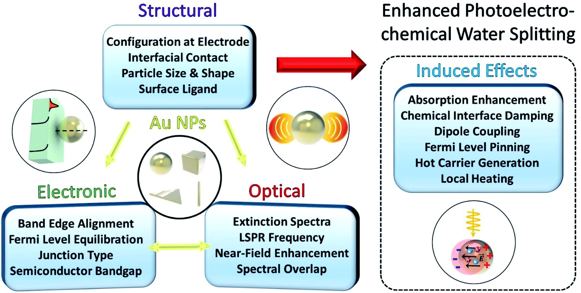 | ||
| Fig. 1 Relations between structural, electronic, and optical properties and processes in Au nanoparticles attached to a semiconductor, which generate various effects contributing to plasmon enhanced photoelectrochemical water splitting. | ||
Fig. 2 shows the various pathways taken by light and charge at the interface in response to a LSPR excitation alongside a brief timeline of their discovery and proposal. Note that, though the schematic illustrates a photoanode, its concepts can be similarly applied to a photocathode. When incident light at the resonance frequency meets the Au NPs, LSPRs are induced in the nanostructure (①). The excitation and relaxation of the LSP induces several effects in the semiconductor (②–⑦) that help generate and transfer charges. Details related to the near-field phenomena (②–⑥) will be described in later sections.
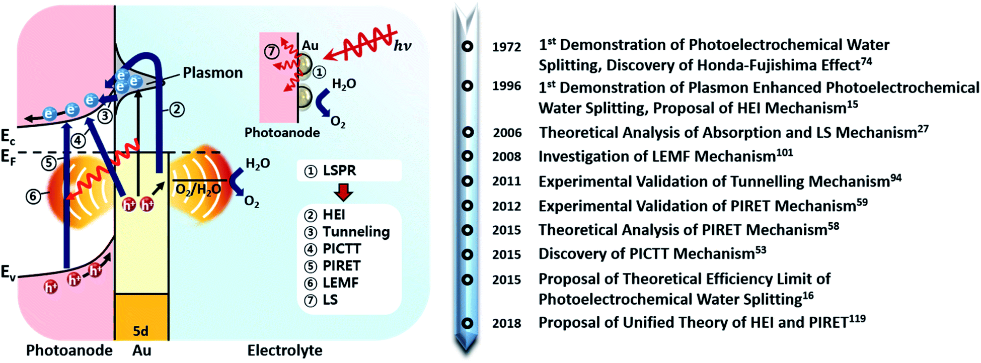 | ||
| Fig. 2 (Left) Possible localized surface plasmon energy transfer mechanism from Au nanoparticles to the photoanode. Abbreviations: hot electron injection (HEI), plasmon induced metal-to-semiconductor interfacial charge transfer transition (PICTT), plasmon induced resonant energy transfer (PIRET), local electromagnetic field enhancement (LEMF), light scattering (LS). (Right) Timeline of key developments in the field of plasmon enhanced photoelectrochemical water splitting. | ||
Herein, we will provide a detailed review of plasmon enhanced photoelectrochemical water splitting with a specific system, that is, Au NPs on a semiconductor. To provide a comprehensive overview, we will review the origin of the plasmonic resonance and optical loss in Au NPs, the various plasmon-induced charge transfer pathways, the formation of Au NPs on semiconductor surfaces and demonstrations of the system in photoelectrochemical water splitting showing enhanced performance relative to the bare semiconductor. Based on these details, strategies to maximize efficiency will be outlined, supported by the latest research results. We finish our review with a brief perspective on practical challenges in the field.
2. Plasmon resonance of Au nanoparticles
2.1 Localized surface plasmon resonance
As discussed earlier, localized surface plasmon resonances (LSPRs) occur in metal nanostructures or nanoparticles in a dielectric environment (Fig. 3a) as a consequence of the coupling of light and electron charges bound to the metal–dielectric interface.18 In the electrostatic limit, the coherent displacement of the electron cloud about the origin in response to the oscillating electric field is of a dipolar nature.19 For a solid spherical particle, this disturbance of the electron cloud due to an applied external electric field can be represented as the polarizability (α).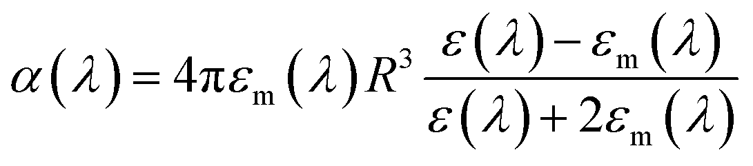 | (3) |
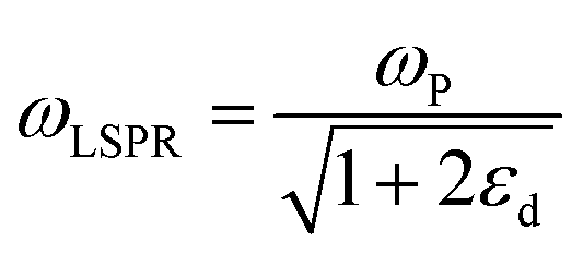 | (4) |
where n is the number density of electrons, ε0 is the permittivity of a vacuum and m is the effective electron mass.22 We note that while the LSPR frequency in eqn (4) represents that of a dipole,23 higher order multipoles can also be excited with increasing ratio of particle size to wavelength.24 At resonance, the absorption and scattering cross-sections of the NPs and electromagnetic fields near the surfaces of NPs experience a dramatic enhancement.25

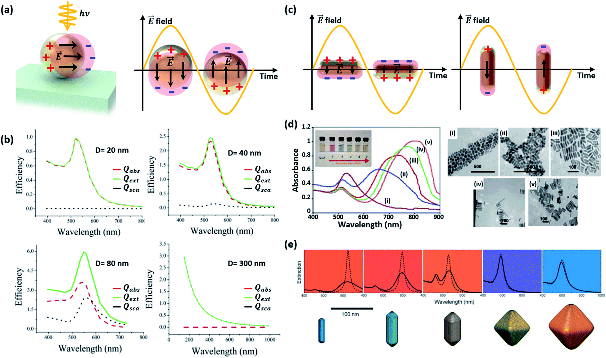 | ||
| Fig. 3 (a) Schematic diagram of a localized surface plasmon resonance (LSPR) excited from a Au nanosphere. (b) Calculated efficiency spectra of extinction Qext, absorption Qabs, and scattering Qsca for Au nanospheres with various sizes (D = 20, 40 and 80 nm). Results for a polystyrene nanosphere (D = 300 nm) are also shown. Reprinted from ref. 27, copyright 2006, with permission from the American Chemical Society. (c) Schematic diagram of LSPR from a Au nanorod. (d) Absorbance spectra (left) and photographs (inset) of aqueous solutions, and TEM images of Au nanorods with various aspect ratios: (i) 1.35 ± 0.32, (ii) 1.95 ± 0.34, (iii) 3.06 ± 0.28, (iv) 3.50 ± 0.29, and (v) 4.42 ± 0.24. Reprinted from ref. 32, copyright 2014, with permission from Elsevier. (e) The colours and extinction spectra of Au NPs with different shapes. Reprinted from ref. 33, copyright 2008, with permission from the Royal Society of Chemistry. | ||
Since the surface plasmon depends sensitively on the surface charge density and distribution on the NP, one can selectively control its resonance by controlling the shape, size, and dimension of the Au NPs. Even before the advent of nanophotonics, the relation between the resonance and size of a Au NP was known from the work of Gustav Mie, which presented analytical solutions to the electromagnetic scattering problem of a spherical particle.26 Recent advances in computational power, nanofabrication and characterization tools over the past two decades have led to a renewal of interest and studies on plasmonic Au NPs.
The LSPR of a spherical Au NP lies in the visible wavelength range, and is generally characterized through the absorption spectrum. As the NP size increases, the scattering and absorption properties undergo marked changes. Fig. 3b exhibits the calculated spectra of extinction, absorption, and scattering efficiency for Au NPs with various diameters (D = 20, 40 and 80 nm).27 For comparison, results of a 300 nm-diameter polystyrene sphere are also shown. The extinction efficiency (Qext) is the sum of the scattering (Qsca) and absorption (Qabs) efficiencies. Below a Au NP size of 10 nm, the absorption and scattering are both weak. When the Au NP size is 20 nm, the scattering is still weak and dipolar (i.e., Rayleigh scattering) while a rising absorption dominates the optical behavior. The resultant color of Au NPs in solution is red. One can see that the extinction efficiency for the Au NP at D = 80 nm is larger than that for a much larger polystyrene sphere with D = 300 nm due to the large LSPR band near ∼530 nm. Although not shown in Fig. 3b, further increases in size lead to a rise and redshift in the scattering spectrum, leading to the appearance of a blue color at a size of around 150 nm. While the spherical model provides good guidelines for predicting the scattering and absorption behavior of a non-spherical Au NP, the accuracy increasingly deviates with increasing NP size. This is due to the emergence of higher order multipolar contributions for larger NPs that are sensitive to the actual shape of the NP.
This size-dependent behavior can influence the light–matter interactions at the interface between the metal and dielectric. Wei and co-workers reported the size-dependent photocatalytic activity of Au NPs on octahedral anatase particles.28 They showed that an increase in the size of Au NPs from 5 to 30 nm led to a gradual increase in photocatalytic performance due to enhanced absorption.
Changes in the Au NP shape rather than the size have a stronger impact on the resonance.29 Elongating the NP into a rod-like shape can drastically alter the behavior of the resonance. As shown in Fig. 3c, two resonances appear from the two distinct dimensions along the longitudinal and transverse axes of the rod. As the longitudinal dimension offers much less confinement than that of the transverse axis, the longitudinal resonance is significantly lower in energy compared to that of the transverse axis.30 Murphy and co-workers synthesized Au nanorods with various aspect ratios and observed the optical properties.31 As shown in Fig. 3d, two different peaks, originating from the longitudinal and transverse plasmon modes, can be easily observed.32 When two Au nanorods are placed nearby without being brought into contact with each other, coupling of plasmon resonances can produce distinct plasmon modes. Fig. 3e shows the extinction spectra of Au NPs with different shapes. The spectrum of the symmetric octahedral Au NPs exhibits a single dominant peak while the spectrum of the rods shows two distinct peaks from the different confinement dimensions.33 In a similar manner, flattening the Au NP along the light incidence direction also blueshifts the resonance because of increased confinement in the compressed dimension.34 The plasmon resonances of other more complex nanostructures featuring shells can be predicted by using the plasmon hybridization model.35 Sharp vertices and edges of Au NPs lead to a field-concentrated dipolar region yielding enhanced electric fields.36 This can help improve the sensitivity of the plasmonic NP to the surrounding refractive index.37 Jeon et al. investigated this effect using Au nanocubes.38 A single Au nanocube with sharp vertices and edges was found to show a higher sensitivity to the refractive index than a Au nanosphere due to enhanced fields at the sharp sites. Furthermore, coupled Au nanorods can support higher responsivities and larger electric field enhancements than solitary Au nanorods due to field confinement between nanorods.
2.2 Plasmon relaxation process
The lifetime of the surface plasmon (SP) is given as39 | (5) |
| Γtot = Γrad + Γnrad | (6) |
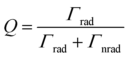 | (7) |
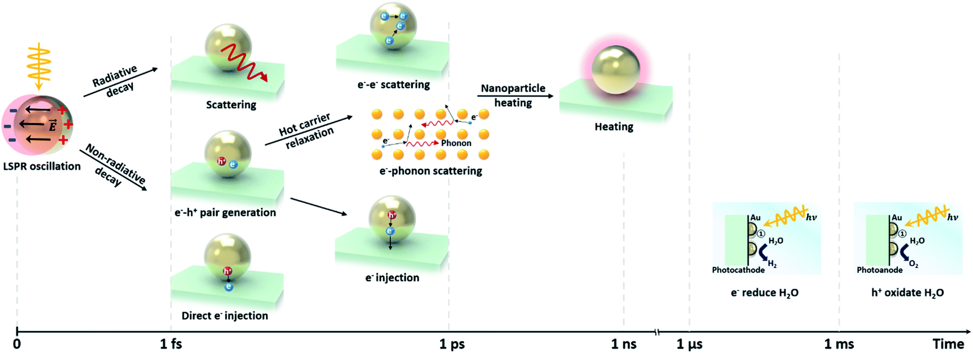 | ||
| Fig. 4 Schematic of the time scale of different plasmon decay processes induced by LSPR-excitation in a plasmonic NP/semiconductor system. | ||
The non-radiative decay is referred to as Landau damping, whose timescale is 1–100 fs.43–46 When a plasmonic NP absorbs light, electron–hole pairs are generated. These hot carriers experience electron–electron scattering (τel ≈ 100 fs to 1 ps) and are in thermal equilibrium with the electron–phonon-heated lattice (τph ≈ 1–10 ps).47–49 The heated plasmonic NP cools down via energy exchange with its surroundings. The cooling time, which depends on the material and size of the plasmonic NP, and the thermal conductivity of the surrounding medium, takes about 100 ps to 10 ns.50,51 Alternatively, if the NP is attached to a semiconductor, the hot carriers from the NP can be injected into it. In order for this process to be more competitive than the electron–electron and electron–phonon scattering processes, the transfer must occur within 1 ps after the LSP generation.52 This process is called indirect electron injection. In contrast, direct electron injection is also possible, which describes the generation of a hot charge carrier from the conduction band of an n-type semiconductor or valence band of a p-type semiconductor in contact with a metallic NP. This process occurs within 20 to 50 fs, which is much faster than indirect injection.53–56 Since the direct and the indirect carrier injection both lead to the generation of additional charge carriers in the semiconductor using sub-bandgap light, application of plasmonic nanoparticles in photoelectrochemical cells is an attractive method for expanding the usable bandwidth of light in photoelectrochemical water splitting.
Another non-radiative decay mechanism is plasmon-induced resonant energy transfer (PIRET), i.e., energy transfer by dipole–dipole coupling. PIRET is a modified form of Förster resonance energy transfer (FRET), which transfers energy from a donor to an acceptor through dipole–dipole coupling.57 The timescale of PIRET is 10 fs.58 The excitons in the semiconductor could be formed by energy transfer from the dipole in a metallic NP to the dipole in a semiconductor.59 This mechanism is influenced by the distance between the NP and semiconductor, the degree of spectral overlap between the emission and absorption, and the orientation of the dipole moments.52 Enhancement by PIRET can be quantified by the number of LSPR-excited carriers in a semiconductor.52
The hot electrons and holes created during the plasmon relaxation process contribute to the water splitting reaction. As shown in Fig. 4, the photoelectrochemical water splitting reaction occurs on a timescale from microseconds to milliseconds.60 The OER process is longer than the HER process because more charges are involved in the reaction. The above mechanisms on charge transfer via plasmon relaxation will be described in detail in Section 3.
2.3 Interband/intraband transition
Non-radiative decay of the LSP occurs via electron transitions between the occupied and unoccupied states of the metal. The electron configuration of a gold atom in the ground state is [Xe]5d106s1, characterized by a fully filled 5d orbital and a partially filled 6s orbital. As a solid, the orbitals hybridize to form a 6sp and a 5d band. These bands are shown in Fig. 5a illustrating the theoretical and experimental band structure for gold, predicted by density functional calculations, quasiparticle self-consistent GW calculations and angle-resolved ultraviolet photoemission measurements.61 The corresponding illustration of the density of states shown in Fig. 5b indicates a narrow 5d band and free-electron-like 6sp band.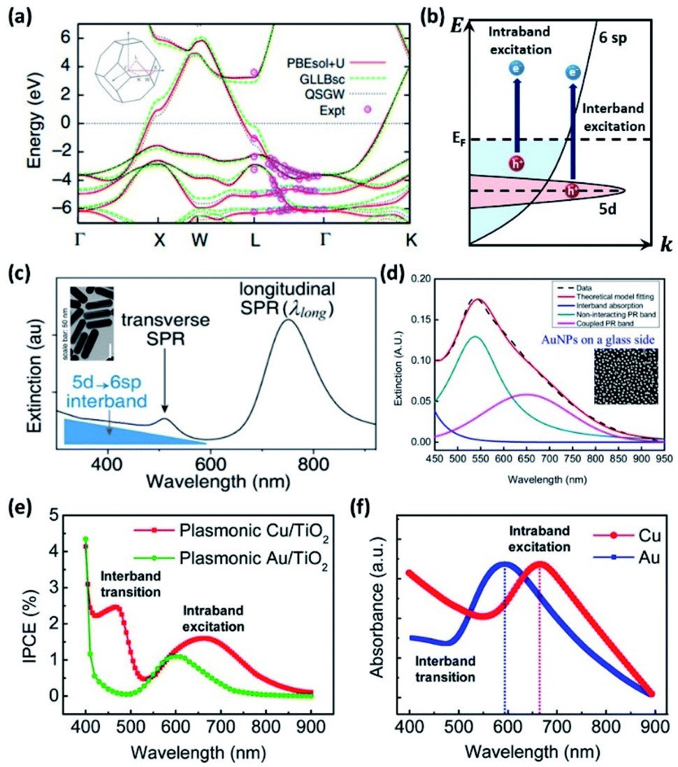 | ||
| Fig. 5 (a) Theoretical energy band structure for Au. Reprinted from ref. 61, copyright 2014, with permission from Nature Research. (b) Schematic diagram of the intraband and interband transitions. (c) Extinction spectra of Au nanorods from interband and intraband transitions. Reprinted from ref. 66, copyright 2017, with permission from the American Chemical Society. (d) Appearance of the coupled plasmon mode of Au NPs due to high surface coverage on SiO2. Reprinted from ref. 67, copyright 2018, with permission from Multidisciplinary Digital Publishing Institute. (e) IPCE from Cu/TiO2 and Au/TiO2 diodes. (f) Absorbance of Cu and Au plasmonic NPs. Reprinted from ref. 68, copyright 2019, with permission from the Royal Society of Chemistry. | ||
A decaying plasmon can deliver energy to excite intraband transitions within the 6sp band or interband transitions between the 5d band and 6sp band. The dominant contribution can be selected by tuning the LSP resonance. Analysis using the Drude model shows that for LSP resonances in the red and infrared range, the absorption is dominated by intraband transitions, while for those in the ultraviolet (UV) and visible range, it is dominated by interband transitions.62,63 Since the LSP resonance is tunable through the shape as described earlier, selection of the dominant transition is possible by controlling the geometry of the NP. These interband and intraband transitions play nontrivial roles in water-splitting reactions by enhancing both the OER and HER performance.61,64,65
The intraband/interband transitions in Au NPs can be separately recognized from the extinction spectra. As shown Fig. 5c,66 a sample of Au nanorods shows two characteristic LSPRs near 480 and 750 nm, corresponding to the transverse and longitudinal modes, respectively. Intraband transitions are dominantly excited by these modes. The background extinction is found to increase for shorter wavelengths, which is attributed to the 5d to 6sp interband transition. By decreasing the particle size down to scales where quantum confinement effects emerge, one can minimize the intraband contribution such that interband transitions become the dominant contribution.54,55 Alternatively, as has been shown for closely distributed Au NPs, the near-field interactions between Au NPs can diminish the normal intraband transition peak by redshifting the coupled resonance peak as shown in Fig. 5d.67
Lee and co-workers distinguished between hot electrons generated from interband and intraband transitions in Cu NPs/TiO2 and Au NPs/TiO2 diodes.68 To achieve this, they measured the incident photon-to-current conversion efficiency (IPCE) using a monochromator system. As shown in Fig. 5e, the IPCE from the Au NPs/TiO2 nanodiode shows one distinct peak at 600 nm, which arises from the intraband transition in agreement with theoretical predictions. On the other hand, the IPCE from Cu/TiO2 has two distinct peaks at 450 and 675 nm, corresponding to interband and intraband excitations. The measured absorbance spectrum provides a more detailed analysis as shown in Fig. 5f. LSPR peaks were observed at 600 and 675 nm for Au and Cu NPs/TiO2, respectively, indicating that intraband transitions were the origin. Absorption peaks were also observed at around 480 nm and 550 nm for Au and Cu NPs/TiO2, respectively, indicating interband excitations. The reason the two absorption peaks are not apparent in the Au NPs/TiO2 IPCE plot is that the electrons excited by the interband transition do not have enough energy to overcome the Schottky barrier height at the metal–semiconductor interface.
Due to the fact that the LSP is, generally, of lower energy than the interband transition, the LSP excitation and decay usually leads to hot carrier generation from intraband transitions. In this case, the distribution of hot electrons and hot holes is created with respect to the Fermi level. Unlike the behavior of intraband transitions, interband transitions leave a hot electron slightly above the Fermi level and a hot hole in the 5d band.66 These hot carriers are quickly thermalized.69 While intraband excitations have been the hot carriers traditionally observed in Au NPs, J. Zhao et al. demonstrated through a photoinduced oxidative etching reaction of Au NPs with FeCl3 that the interband transitions are a more efficient pathway toward hot carrier generation in addition to offering a higher catalytic reactivity.
Another important factor related to the electron transitions in the Au is the size of NPs. Since the hot charge carriers generated by intraband transitions have a mean free path of 10–40 nm, most hot carriers in plasmonic NPs (<20 nm) can reach the NP surface before thermalization. On the other hand, hot charge carriers generated by interband transitions have a shorter mean free path (∼1 nm), necessitating the use of smaller NPs (2–3 nm) for charge extraction.
In summary, an improved understanding of the origin of hot carriers is beneficial for designing efficient photoelectrochemical water splitting systems. The type of transition should be considered when selecting the semiconductor material, the range and frequency of usable light, and shape of the Au NP. These insights should provide strategies for efficient injection of hot carriers into semiconductors. The junction between the plasmonic NP and semiconductor is another important factor to consider. A suitable semiconductor that can selectively isolate the photogenerated carriers to enhance their lifetimes must be found.70,71 This will be described in detail in Section 3.
3. Mechanisms of plasmon enhanced photoelectrochemical water splitting
3.1 Exceeding the Shockley–Queisser (SQ) limit
The theoretical photoelectrical conversion efficiency was first proposed by William Shockley and Hans-Joachim Queisser (1961).72 For a simple ideal p–n junction solar cell with a 1.1 eV bandgap, the maximum achievable efficiency (referred to as the detailed balance limit) was found to be 30%, assuming (1) one electron–hole pair excitation per photon, (2) 100% radiative recombination, and (3) no loss of generated carriers. Obviously, these assumptions correspond to an idealized scenario, and for this reason, the Shockley–Queisser (SQ) limit represents an upper bound to practical conversion efficiencies. To obtain the conversion efficiency of a solar cell (ηSC) with a solar light standard (AM 1.5 G; ASTM International Standard G173-03), one can calculate the ratio of generated electrical power (WG) to incident light power (WI), that is, ηSC = WG/WI (Fig. 6a).73 | ||
| Fig. 6 (a) Detailed balance limit of a solar cell operated at 298.15 K and illuminated with AM 1.5 G sunlight plotted against bandgap wavelength (upper) and bandgap energy (lower). Adapted from ref. 74, copyright 2016, with permission from Elsevier. (b) Maximum harvested solar-energy percentage of semiconductor absorbers with respect to the bandgap energy (upper). Maximum STH efficiencies (solar to hydrogen conversion efficiencies) of single absorber photoelectrochemical cells (lower). Adapted from ref. 78, copyright 2018, with permission from the American Physical Society. (c) Maximum solar energy conversion efficiency for plasmon enhanced photoelectrochemical water splitting (dark blue curve), bare semiconductor (grey curve) and the Shockley–Queisser limit (light blue curve) plotted against bandgap energy. Reproduced from ref. 16, copyright 2015, with permission from the PCCP Owner Societies. | ||
The discovery of water decomposition using TiO2 by Fujishima and Honda in 1972 stimulated new research efforts on photoelectrochemical water splitting.74 In particular, efforts have been dedicated to finding the theoretical efficiency limits of photoelectrochemical water splitting. Bolton et al. first summarized the ideal limits of photoelectrochemical water splitting in 1985.75 The excited states were assumed to reach equilibrium with the surroundings very quickly and reversibly, while the hot carrier effect was disregarded. The ideal solar energy conversion efficiency was defined using the formula below, where Jg is the absorbed photon flux, μex is the excess chemical potential generated in the system by absorption of light, ϕconv is the photon to product conversion quantum yield, and S is the total incident solar irradiance.
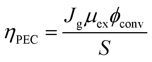 | (8) |
The above theoretical efficiency has been refined in recent days to include more detailed experimental conditions. For example, even the absorption of water was considered in 2014.76 Jacobsson et al. included losses (carrier separation, carrier transportation, and reaction overpotential) during photon absorption for carrier excitation and showed an expected solar to hydrogen (STH) conversion efficiency (ηPEC) of 17.8% in one-bandgap (single-cell) devices in 2015.77 It was shown that even for an idealized situation the STH efficiency could not reach 100% as shown in Fig. 6b.78 In 2016, Fountaine's group suggested a unified framework to establish the theoretical efficiency limit for photoelectrochemical water splitting cells.79 For a device operating at some potential Erxn at a faradaic efficiency fFE with a corresponding operating current of jop under an incident solar power of WI, the efficiency is calculated as follows.
 | (9) |
Strategies to improve the efficiency can be found from insights gained from photovoltaic (PV) cells. PV cells and photoelectrochemical cells both share the key principle of producing work by generating electron–hole pairs through light absorption, separation, and recombination. The use of a multi-junction cell is a straightforward way to increase the PV efficiency by expanding the bandwidth of harnessable light.80 However, even with a single PV semiconductor, one can beat the SQ limit by considering ways to overcome the basic assumptions used to define it. These could include (1) multi-electron–hole-pair generation, (2) hot carrier excitation and collection, and (3) use of nanostructures rather than a planar structure. In a similar manner, multiple exciton generation (MEG) in quantum dots has been reported to exceed 100% quantum yield.81 Plasmons can generate two or more excitons when the resonance is tuned to the bandgap energy and the phonon emission is prohibited.82 There have been several reports of multiple electron–hole pair generation processes during plasmon excitation–decay. Linic's group in 2012 observed a super-linear photocatalytic rate dependence on illumination source intensity for an ethylene oxidation reaction with a plasmonic Ag nanocube, and attributed this phenomenon to multiple electron excitations mediated by the plasmon.83 A plasmon-induced two-electron reaction was also reported for Au NPs in the presence of a hole scavenger during carbon dioxide reduction (2018).84 Compared to conventional dielectrics where the mode volume (vm) is limited to ∼(λ/2)3, a plasmonic NP offers an ultrasmall mode volume via tight light confinement corresponding to a large density of optical states.85 The light concentrating properties of plasmonic gold NPs have great potential for driving water splitting reactions beyond the SQ limit.16,86 A density matrix model developed by Cushing et al. showed that the photochemical conversion efficiency that takes into account the various plasmonic effects can be greater than the SQ limit above the practical band gap energy of 2 eV required for water splitting (Fig. 6c).16
3.2 Hot carrier injection (HCI)
Through Landau damping discussed earlier, a plasmon resonance at a frequency ω can excite electron–hole pairs in the metal with energy distributions of EF ∼ (EF + ℏω) for electrons and (EF − ℏω) ∼ EF for holes.69,87 Such energetic charge carriers are referred to as hot carriers (e.g., hot electrons or hot holes). The hot carriers can exchange their energy with the environment to reach an equilibrium carrier energy distribution.Hot carrier injection (HCI) refers to the transfer of an excited carrier from a metal to an interfacing semiconductor by overcoming the Schottky barrier with sufficient kinetic energy. Hot electron and hole injection are abbreviated as HEI and HHI, respectively. The Fermi levels of the semiconductor and metal in their isolated states are written as EF,semi and EF,metal, respectively. To activate HCI in plasmon enhanced water splitting, several electronic factors must be considered including (1) Fermi level alignment between the metal and semiconductor, (2) band bending at the interface and (3) carrier momentum along the carrier flow direction. The generated carriers should be separated at the metal–semiconductor interface. Let us consider an n-type semiconductor and a plasmonic metal for this system. When EF,semi ≤ EF,metal, an ohmic contact is formed at the interface between the metal and semiconductor, characterized by the conduction and valence bands of the semiconductor bending downward near the interface (Fig. 7a).88 Hot electrons that are generated from the metal through plasmon damping may transfer across the interface into the semiconductor, but will return to the metal due to the electric field in the space charge region. Therefore, plasmon enhanced photoelectrochemical water splitting will not occur in this situation. On the other hand, when EF,semi > EF,metal, a Schottky contact is formed at the interface. Here, the conduction and valence bands bend upward near the interface. A hot electron with enough kinetic energy to overcome the Schottky barrier can be injected into the semiconductor, where it can drift away from the metal in accordance to the electric field of the space charge region. In this configuration, efficient charge separation is enabled as shown in Fig. 7a. The electronic band picture can be extended to treat redox chemistry at the surface of the metal. The equilibrium band structure of an n-type semiconductor joined to a metal with a work function W in a chemical environment comprising a redox pair (D/D+) with an electrochemical potential Eredox is presented in Fig. 7d (EF,semi > Eredox > EF,metal).88
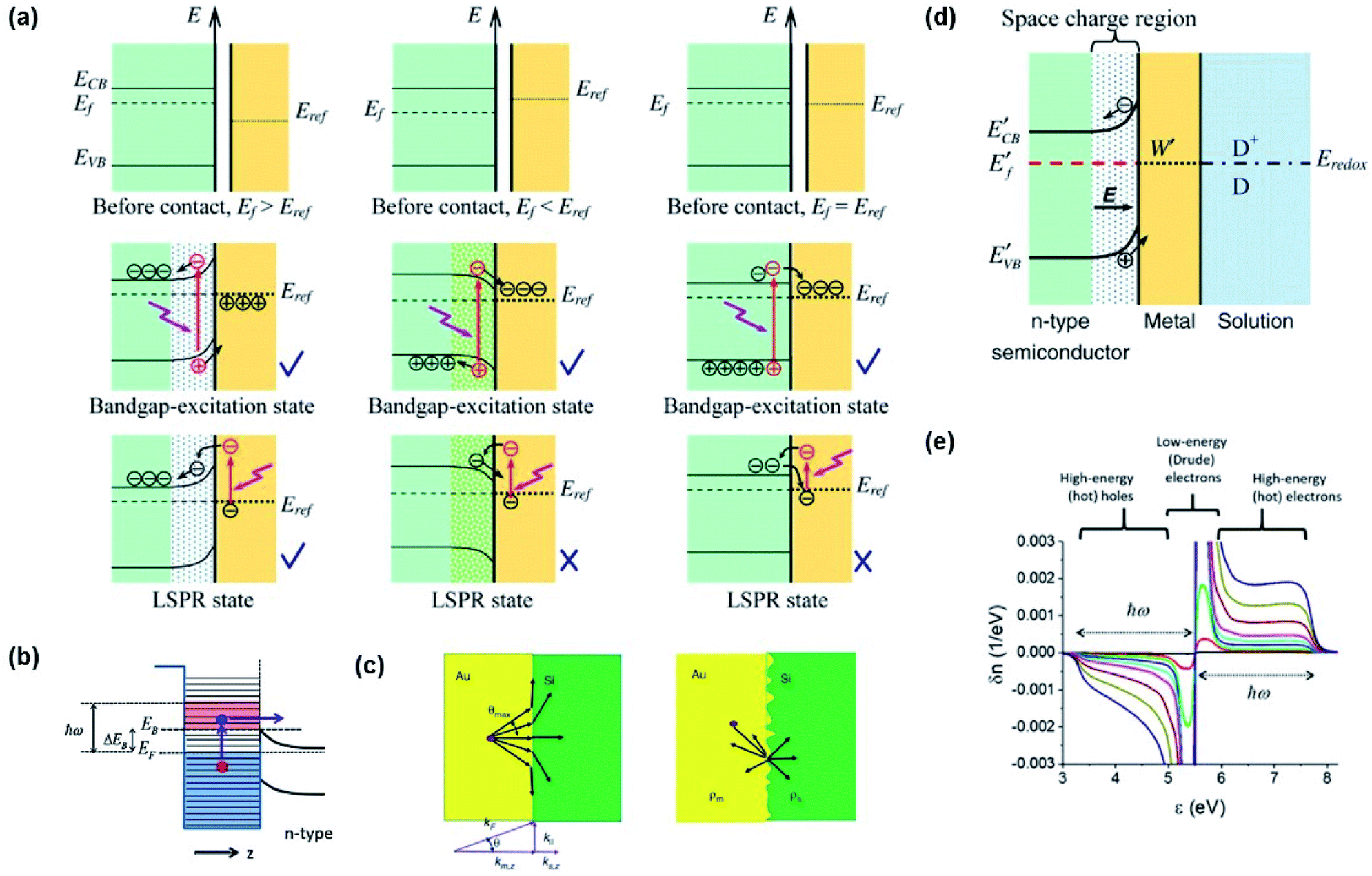 | ||
| Fig. 7 (a) Band diagrams of several cases (EF,semi > EF,metal (left), EF,semi < EF,metal (middle), and EF,semi = EF,metal (right)) for charge carrier separation at the metal–semiconductor interface. Reprinted from ref. 88, copyright 2013, with permission from Institute of Physics Publishing. (b) Band diagram for hot electron injection over the Schottky barrier. Reprinted from ref. 62, copyright 2014, with permission from Elsevier. (c) Angular pathways of carrier injection at smooth (left) and rough surfaces (right). Reprinted from ref. 89, copyright 2020, with permission from De Gruyter. (d) Band diagram showing the band alignment of the electrolyte, Au nanoparticle, and semiconductor. Reprinted from ref. 88, copyright 2013, with permission from Institute of Physics Publishing. (e) Plasmon induced hot carrier distribution around the Fermi level in a Au nanosphere. Reprinted from ref. 92, copyright 2017, with permission from the American Chemical Society. | ||
We describe the detailed constraints for charge transfer from the metal into the semiconductor. The Schottky barrier is the energy difference between the conduction band at the interface and the metal Fermi level (ΔEB = EB − EF,metal). To overcome this barrier, the energy of the hot carrier, E, partially or fully attained through the photon energy, should be higher than that of the barrier height (ℏω0 ≥ E − EF,metal ≥ ΔEB). The corresponding energy levels are depicted in Fig. 7b.62,89 One must also consider the momentum of the charge carriers as they also provide an additional constraint for charge transfer. From the energy relations, one can find the momentum that is needed for the carrier to overcome the Schottky barrier 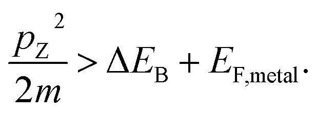 This defines the injection cone of hot electrons that can overcome the barrier, characterized by the angle,
  90 One way to bypass this additional constraint on the injection angle is to introduce a rough surface as shown in Fig. 7c.89 Such a surface allows charge carriers outside the injection cone to be scattered into the semiconductor by endowing them with the appropriate momentum.
The energy distribution of hot carriers depends on the size and shape of the Au NP. For a spherical plasmonic NP in the dipole limit, the hot carrier generation rate (RHCG) can be derived as
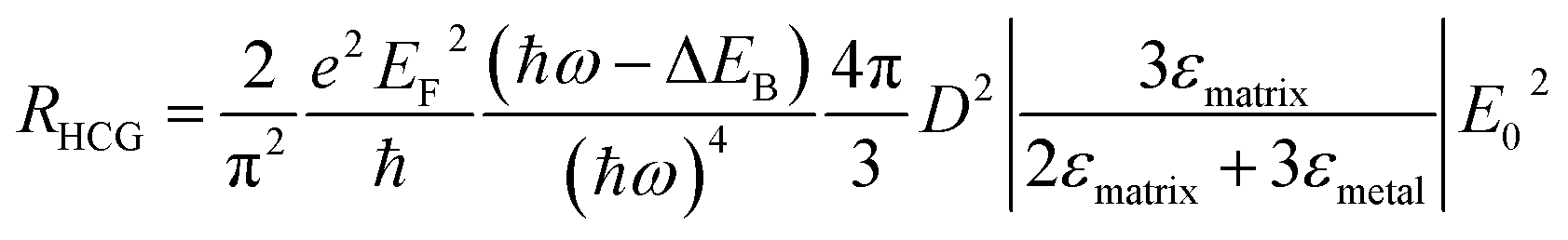 | (10) |
3.3 Quantum tunneling injection
If the energy of a hot carrier (E) is lower than the Schottky barrier height (for hot electrons; E − EF,metal < ΔEB), carrier injection from the metal to the semiconductor is classically forbidden. However, when the scales of interest are a few nanometers, hot carriers may penetrate through the Schottky barrier by quantum tunneling as shown in Fig. 8a. Therefore, decreasing the Schottky barrier height and depletion width is essential to observe this effect.94 This effect can also appear more pronounced at very high dopant concentrations. | ||
| Fig. 8 (a) Band diagram picture of hot electron injection at the Au–TiO2 heterojunction by (A) transfer over the barrier or (B) tunneling. Reproduced from ref. 96, copyright 2017, with permission from the Royal Society of Chemistry. (b) Tunnelling probability at the Au–TiO2 interface as a function of electron energy for different doping concentrations. Reprinted from ref. 90, copyright 2018, with permission from Elsevier. | ||
In 2011, photosensitization of TiO2 with embedded Au NPs was reported to result in an increase in TiO2 conductance by over 1000-fold when illuminated by 600 nm light due to hot electron tunneling.95 It was found that a hot carrier tunnels through the barrier into an unoccupied defect state formed in the depletion region.96,97
The tunneling probability is highly dependent on the dopant concentration of the semiconductor. Theoretical calculations of the tunneling probabilities at a Au (10 nm)–TiO2 junction were performed using the transfer matrix formalism. The results showed that the probability of tunneling increases with dopant concentration as shown in Fig. 8b.90 It is worth noting that tunneling through Schottky barriers is a commonly observed phenomenon in photocurrent measurement of nanoscale metal contacts on degenerately doped nanostructured devices.
3.4 Local electromagnetic field enhancement (LEMF)
One of the most prominent features of an LSPR is the enhanced local electromagnetic field associated with the resonance.98–101 The effect is characterized by a strong near-field intensity at the surface of the plasmonic NP. This region of high local electric field is referred to as a “hot spot” as shown in Fig. 9a and depends on the shape and size of the metal NP and the polarization direction of the incident field.102 The electric field in a hot spot possesses an intensity that can be up to several orders higher than the incident field, which is useful for enhancing various optical signals in neighboring systems including Raman, fluorescence and nonlinear intensities. If the hot spot is located near a semiconductor and has energy above the bandgap (Eg < ℏω), electron–hole pairs in the semiconductor can be locally generated at an enhanced rate proportional to the square of the electric field (|E|2) intensity.103 This radiative mechanism is distinct from those describing hot carrier transfer from the metal into the semiconductor. To harness the energy in the hot spot more effectively, it is necessary to visualize its distribution and use it to configure the contact geometry between the metal and semiconductor. The field intensity decays exponentially with distance. This distance is characterized by the decay length (Ld), which dictates the interaction length between the semiconductor and metal NP. As the decay length is a function of the hot spot intensity, it can be tuned by varying the NP shape and can increase with NP size (Fig. 9b).104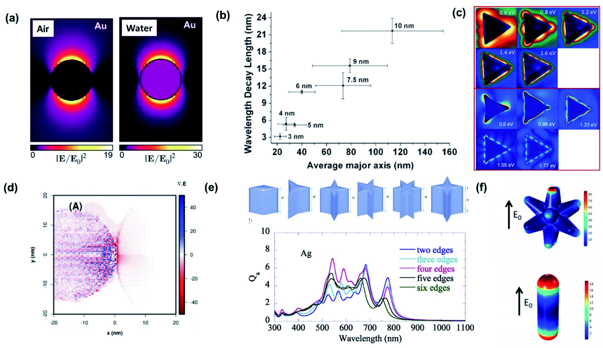 | ||
| Fig. 9 (a) Near-field enhancement simulation (λ = 522 nm) by the Boundary Element Method (BEM) of a 20 nm-diameter Au nanoparticle embedded in a vacuum (n = 1) and water (n = 1.33). Reprinted from ref. 102, copyright 2015, with permission from the American Chemical Society. (b) Plasmon decay length vs. average axis length of Au nanoislands. Nominal thickness is indicated. Reprinted from ref. 104, copyright 2011, with permission from the American Chemical Society. (c) Comparison of experimental (upper) and simulated (lower) mode profiles measured with electron-energy-loss spectroscopy. Reprinted from ref. 108, copyright 2011, with permission from the American Physical Society. (d) Theoretical representation of the charge densities by means of the divergence of the local electric field for Ag NPs loaded on TiO2. Reprinted from ref. 99, copyright 2018, with permission from the Royal Society of Chemistry. (e) Absorption efficiency (Qa) of nanoparticles with sharp edges. Reprinted from ref. 109, copyright 2020, with permission from Elsevier. (f) Surface maps of the normal electric fields of Au nanostars (upper) and Au nanorods (lower). Reprinted from ref. 111, copyright 2020, with permission from the American Chemical Society. | ||
The hot spot distribution of a plasmonic NP can be easily predicted through simulations including the finite-difference time-domain (FDTD) algorithm and discrete dipole approximation (DDA).105 Direct imaging of the spatial distribution is another matter. Due to the subwavelength size of the NP, imaging the fields with light is a challenging task since the resolution is diffraction-limited to ∼λ/2. Near-field scanning optical microscopy (NSOM) offers ways to overcome this limit by operating with a resolution that is no longer defined by wave optics but by the probe aperture size. However, since the signal and aperture size are inversely related, improvements in resolution are followed by decreases in signal-to-noise ratios. The use of fast electrons instead of light is an alternative but powerful route toward imaging the hot spots with substantially improved resolution that can reach atomic scales. By combining electron energy loss spectroscopy (EELS) with transmission electron microscopy (TEM) or scanning transmission electron microscopy (STEM), the local hot spots arising in plasmonic NPs can be spatially and spectrally resolved (Fig. 9c).106–108
For the case where the plasmonic NP is close to a semiconductor, understanding the hot spot distribution can assist in identifying where the electron–hole pair generation occurs in the semiconductor. Fig. 9d presents calculations of the LSPR-induced charge density distribution in a TiO2 nanosphere (left) next to a Ag NP (right). The plot was obtained by calculating the divergence of the local electric field.99 It is clear that the generation rate of electron–hole pairs is maximum closest to the plasmonic NP, and it decreases as we move away from it.
The increased number of sharp edges does not guarantee a higher absorption efficiency (Fig. 9e).109 To enhance the hot spot intensity of a single plasmonic NP, one can devise schemes to introduce a strong potential gradient in the NP, which can lead to the so-called ‘lightning-rod effect’. This can be accomplished by introducing a smaller radius of curvature or sharper edge in the NP. A decreased edge sharpness generally leads to a blue-shift in LSPR due to a reduced electron oscillation path length (or characteristic particle size), and decreased field intensity due to a weakening of the lightning-rod effect.109,110 The addition of spikes on a NP, that transforms the NP into a nanostar, is an effective route for enhancing the hot spot intensities. This is evident from comparisons between a conventional spherical Au NP and a nanostar sharing the same LSPR and volume, demonstrating superior hot spot intensities and hot electron generation rates for the nanostar as shown in Fig. 9f.111
3.5 Plasmon induced resonant energy transfer (PIRET)
For a coupled metal NP–semiconductor system, electronic transitions in the semiconductor are possible even with sub-bandgap photon energies (Eg > ℏω) if there is partial spectral overlap between the LSPR and semiconductor absorption. The dipole moment associated with the LSPR in the plasmonic metal NP can transfer its energy non-radiatively via dipole–dipole coupling to the neighboring semiconductor, resulting in an interband excitation. This mechanism is distinct from that of Förster resonance energy transfer (FRET), which is characterized by a dipole–dipole mediated energy transfer from a higher-energy donor (emitter) to a lower-energy acceptor (absorber). FRET applied to the coupled metal NP–semiconductor system would refer to an energy transfer from the semiconductor to the metal, and the process would serve as a quenching mechanism for the semiconductor because it describes energy leaving the semiconductor. In contrast to the FRET mechanism, energy transfer can occur in the reverse direction from the plasmonic NP (lower-energy donor) to the semiconductor (higher-energy acceptor) by dipole–dipole coupling. This process is referred to as plasmon induced resonant energy transfer (PIRET), and affords one the ability to induce charge carriers in the semiconductor without direct contact or above-bandgap light. The excitation of PIRET depends on the separation distance between the semiconductor and metal NP, the dephasing time of the plasmon, and the recombination time of the semiconductor.58,59The energy transfer rate from the donor to the acceptor can be theoretically described by the well-known Förster theory. The Förster critical distance (R0) is defined as the distance corresponding to 50% of energy transfer. The energy transfer rate (w) from the above resonant energy transfer process including FRET (wFRET) and PIRET (wPIRET) is represented by58
 | (11) |
 | (12) |
 | (13) |
 dependence. Furthermore, enhancing the plasmonic absorption of the Au NP through geometrical means while using a semiconductor with a low absorption coefficient can boost the efficiency.
In realistic situations, PIRET and FRET compete with each other in plasmon mediated reactions such as plasmon enhanced photoelectrochemical water splitting. FRET and PIRET should lower and raise the gain factor in the semiconductor exciton population, respectively (ΔNFRET < 1, ΔNPIRET > 1). The net gain of the exciton in the semiconductor near the plasmonic metal nanoparticle with PIRET and FRET mechanisms can be expressed as follows using the energy-transfer efficiency formula (i.e., ΔN = (1 − EFRET) × (1 + EPIRET)):112
 | (14) |
 | (15) |
3.6 Plasmon induced metal-to-semiconductor interfacial charge transfer transition (PICTT)
In 2014, Long and Prezhdo suggested a new instantaneous charge separation pathway using time-domain density functional theory with nonadiabatic molecular dynamics in a Au–TiO2 system (Fig. 10a).54 The authors theoretically showed a high probability (50%) of the photoinduced plasmon delocalizing into the TiO2 surface, thereby realizing the instantaneous appearance of an electron in the semiconductor without requiring the traditional steps of electron–hole pair generation in the metal and carrier transfer across the interface. In 2015, Lian and co-workers proved the process in a CdSe nanorod–Au NP system and recorded a quantum efficiency of around 24%.53 They named the process plasmon-induced interfacial charge-transfer transition (PICTT). As we discussed earlier, HCI is another process through which carriers can be introduced into the semiconductor by means of LSPR. As both processes, HCI and PICTT, describe the plasmon-mediated appearance of an electron in the semiconductor, it is important to understand how to select between the two. Z. Zhang et al. showed that PICTT is dominant when the metal and semiconductor share a strong chemical interaction, while HCI is dominant when the van der Waals interaction is significant.113 In the case where these two interfacial processes coexist, the polarization direction of the plasmon plays a crucial role in determining which process is more dominant (Fig. 10b).114 Using non-adiabatic molecular dynamics simulations, J. Zhang et al. demonstrated that parallel and perpendicular polarizations with respect to the semiconductor surface give rise to HCI and PICTT, respectively.114 PICTT can be of significance in plasmon enhanced device applications. For example, a plasmonic phototransistor with a significantly high photoresponsivity of 22.3 A W−1 was reported using Si–(Au@MoS2), and its performance was attributed to the enhanced optical and electronic device properties and the possible realization of HCI and PICTT.115 | ||
| Fig. 10 (a) Schematic of possible electron transfer pathways from a donor to an acceptor. (Red) Adiabatic transfer over a transition state barrier. (Blue) Non-adiabatic transfer via hopping between donor and acceptor states. Reprinted from ref. 54, copyright 2014, with permission from the American Chemical Society. (b) Schematic of the PICTT mechanism. IV and V indicate the interfacial hot-electron transfer from a cluster to a semiconductor and the charge diffusion back from the semiconductor to the cluster, respectively. Reprinted from ref. 114, copyright 2019, with permission from the American Chemical Society. | ||
3.7 Remarks on the unified mechanism
In 2013, Li's group showed synergetic photocatalytic activity in TiO2 NPs decorated with smaller Au NPs from UV and visible light illumination. The photocatalytic performance under the two different bands of light was better than the combined performance under each band.116 Since sub-bandgap light was used, this result suggested the presence of another mechanism besides the plasmon enhanced photocatalytic mechanism but it was not fully understood. The result is now attributed to the contribution of two different plasmon-induced charge transfer mechanisms, PIRET and HCI, which are not dictated by the bandgap of TiO2.117 In a similar manner, Wu's group suggested the combination of PIRET and hot carrier injection (HCI) processes operating in a Ag@Cu2O NP system.118 Transient absorption spectra were measured for various shell thicknesses to determine the dominant mechanism. Since PIRET reflects the overlap between the LSPR and Cu2O interband transition and HCI follows the LSPR, one can identify the two mechanisms by tuning the LSPR with the Cu2O shell thickness. For thin shells, a significant overlap between the LSPR and Cu2O band edge was found to allow PIRET and HCI to both contribute to charge transfer. The competition between the two processes was found to adversely affect the photocatalytic activity. On the other hand, a thicker shell redshifted the LSPR, separating the two contributions. This effect was found to be synergetic, enhancing the photocatalytic activity.X. You et al. developed a unified theoretical framework for HCI and PIRET.119 The authors showed that the two processes could be distinguished by the line-shape, where PIRET showed an asymmetric Fano-type line shape due to the interference between the external and plasmon-induced electric fields and HCI showed a Lorentzian line shape for the plasmon. These results help guide the design of coupled metal–semiconductor architectures and allow one to target the wavelengths of interest without compromising the photocatalytic performance.
4. Formation of the semiconductor and Au nanoparticle interface
4.1 Au nanoparticle direct contact formation methods
Direct contact between Au NPs of a desired shape and a target substrate can be achieved through a variety of methods. Here, we emphasize two types of popular method that do not involve any ‘buffer’ in the contact between Au and the substrate: physical vapour deposition (PVD) and solution-based techniques.One of the simplest ways to create Au NPs directly on a substrate is through the process of coalescence starting with an ultrathin Au film. On a nonwetted surface, a deposited ultrathin Au film is energetically metastable such that rather than forming a uniform planar sheet, it forms an irregular complex morphology including holes. Annealing the film at high temperatures induces a morphological transformation of the film into isolated sphere-like Au nanoislands, as the system tries to reduce its total energy by minimizing the surface area. As shown in Fig. 11a, a Au nanoisland with an average size of about 22 nm was obtained on a ZnO substrate by this process. The ultrathin Au film was prepared by thermal evaporation on a ZnO layer, and was heated to 250 °C for 2 hours under vacuum.120 Picosecond decay dynamics from laser pumping showed an increase in the intraband and decrease in the interband electron transfer rates with increasing Au NP size. Since the transformation from film to island is dependent on the temperature, the annealing temperature provides a degree of control over the shape and spacing of the Au nanoislands.121 Similarly, the thickness of the Au film can also be used to control the geometrical parameters of the Au nanoislands. H. Robatjazi et al. prepared Au films with 2, 6, and 10 nm thicknesses on a NiOx layer by E-beam evaporation and subsequently heat treated them at 300 °C for 1 hour. Fig. 11b shows the morphology of the heat-treated 2 nm-thick film, where Au NPs with an average size of 10 nm are observable.122
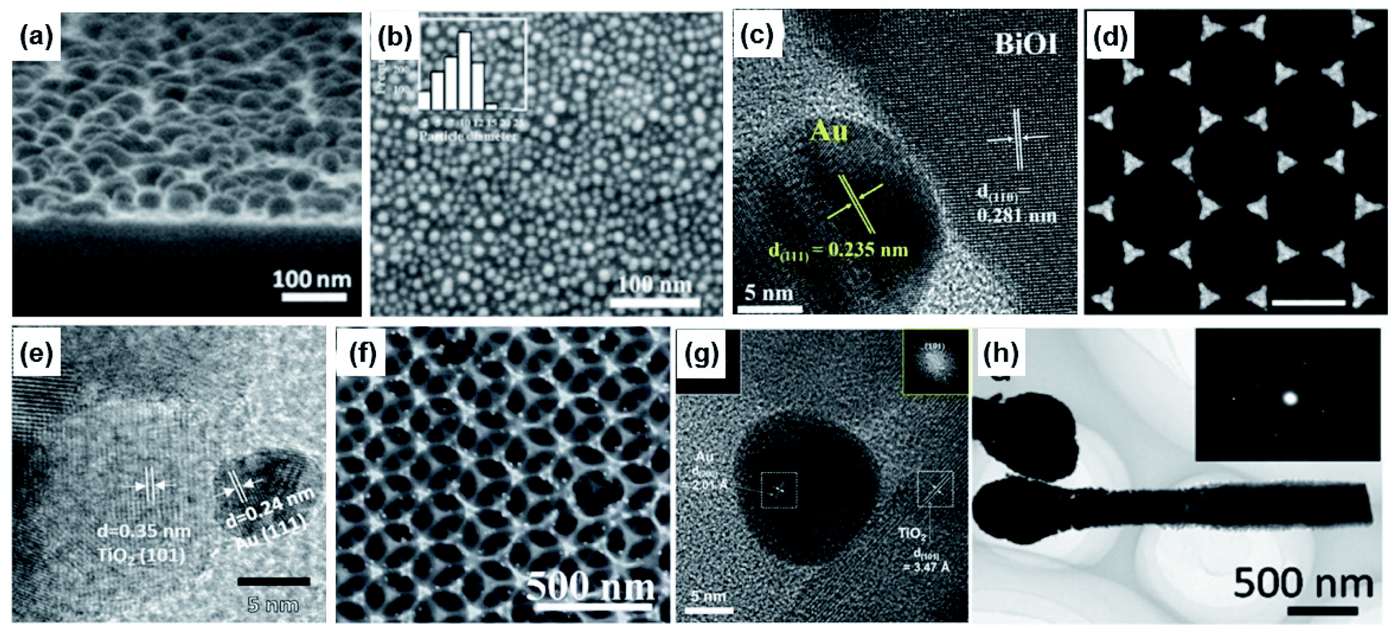 | ||
| Fig. 11 Methods to form direct contact between Au nanoparticles and photoactive semiconductors: (a) sputtering and post-heating. Reprinted from ref. 120, copyright 2020, with permission from the American Institute of Physics. (b) E-beam evaporation and post-heating. Reprinted from ref. 122, copyright 2015, with permission from the American Chemical Society. (c) Short-time sputtering. Reprinted from ref. 123, copyright 2021, with permission from the American Chemical Society. (d) E-beam evaporation and masking. Reprinted from ref. 124, copyright 2021, with permission from the American Chemical Society. (e) Pulsed laser ablation in liquids. Reprinted from ref. 127, copyright 2018, with permission from the American Chemical Society. (f) Thermal reduction. Reprinted from ref. 129, copyright 2014, with permission from the Royal Society of Chemistry. (g) Chemical reduction from the nearby medium. Reprinted from ref. 130, copyright 2020, with permission from the American Chemical Society. (h) Photoreduction. Reprinted from ref. 131, copyright 2014, with permission from the American Chemical Society. | ||
Even without heat treatment, Au NPs can be directly formed on substrates with low surface energy. An example can be found in Au sputtered onto a bismuth oxyiodide nanoflake. Fig. 11c shows a TEM image illustrating a Au NP, identifiable by the Au (111) lattice, prepared on the BiOI nanoflake through sputtering.123 Here, the sputtering time (i.e., sputtered mass) was used to control the coverage density and average Au NP size.
It is clear that the spheres are the energetically favored shapes for Au deposited on nonwetted substrates. Complex shapes other than spheres with the desired order and spacing can also be created with the use of templates. Templates or masks can be created using top-down approaches such as E-beam lithography or bottom-up approaches relying on self-assembly of nanostructures. Self-assembly is particularly attractive because it is low-cost, scalable and easily implementable. A common example is the self-assembled formation of a hexagonal lattice with polystyrene nanospheres on a substrate. An inverse pattern comprising an arrangement of triangular Au nanoprisms can be created through the deposition of Au and subsequent removal of the polystyrene spheres (Fig. 11d). More sophisticated control over the shape of the Au NPs is possible by controlling the Au deposition parameters including the evaporation rate and angles.124,125 A major benefit of using a template is that the desired shape for the Au nanostructure can be achieved without a post-heat treatment process. This is especially useful if the Au NPs are to be used in devices that can suffer damage under high temperatures.
Solution-based methods may offer more accessibility than PVD techniques for the preparation of Au NPs on a target substrate since the latter often require ultrahigh vacuum conditions. Pulsed laser ablation in liquids (PLAL) is a method for producing a dispersion of Au NPs with narrow size distributions in solution without the use of surfactants. To form the Au NPs, a high-power laser pulse is applied to a bulk Au pallet contained in the solution. The NP size distribution and yield can be controlled by the PLAL duration. If the process is carried out for a long time, the NP size distribution becomes narrow, and Au NP yield increases. The formed particles are relatively stable in solution for more than 1 month despite having no capping agent. This stability is due to surface passivation by hydroxyl groups (OH−) in water.126 Attaching the Au NPs to a target substrate can be easily accomplished by inserting the substrate into the as-formed Au NP solution and allowing the Au NPs to drift and diffuse toward it (Fig. 11e).127 The advantage of the PLAL process is that the Au NPs carry no capping agent, and therefore direct contact between the Au NP and substrate is achievable.
Another popular method for attaching Au NPs to a substrate with homogeneous coverage is through the process of ionic layer adsorption and thermal reduction (ILATR). The method involves the sequential steps of dipping the substrate into a solution containing gold ions which forms an adsorbed ionic layer on the surface, drying it, and introducing it into an ethanol–water mixture heated to a temperature of 100 °C or higher. This process allows the adsorbed Au ions at the surface layer to be reduced by ethanol into Au NPs with average sizes of 10 nm or less.128 The Au NP coverage is homogeneous throughout the substrate surface as a result of the homogeneity of the adsorbed ionic layer. This method is especially useful for preparing Au NPs on nonplanar structures featuring complex morphologies, in contrast to vacuum deposition methods which allow Au to only be deposited in areas within the line of sight from the Au target. Fig. 11f demonstrates the successful preparation of a 3D photoanode homogeneously decorated with Au NPs using the processes of ILATR.129
It is clear that other reducing agents besides ethanol can be used to reduce Au ions into Au NPs. For example, the curing agent used to solidify poly(dimethylsiloxane) (PDMS) reduces Au ions. S. Y. Lee et al. created a porous PDMS sponge loaded with TiO2 and Au NPs as a plasmonic photocatalyst, where the Au NPs were created by the reducing power of the PDMS curing agent (Fig. 11g).130
If the Au ions are attached to a semiconductor, above-bandgap light can also be used as a reducing agent. Photoreduction of Au NPs onto ZnO nanorods is a good example. It was shown that illuminating ZnO nanorods immersed in a Au ion solution with a 300 W xenon lamp resulted in a coating of Au NPs on the surface of the ZnO nanorods (Fig. 11h).131 In this case, electrons in the ZnO, photoexcited into the conduction band, are transported to the interface and used in the reduction of the attached Au ions.
As shown in the above examples, there are many methods to directly attach Au NPs to a surface. However, challenges still remain in achieving precise control over the shape, coverage, and size of the NP, which continues to stimulate research activity dedicated to this area.
4.2 Fermi level pinning
The barrier height of a Schottky junction formed at the metal and semiconductor contact can be found as follows:| qϕb = q(ϕm − χ) = EF,m − EC | (16) |
In 2011, Tu et al. showed the photoelectrochemical properties of a GaN substrate pinned by Au NPs in a 1 M HCl aqueous solution as summarized in Fig. 12a.135 In this case, contact between Au NPs and the GaN substrate introduced metal induced gap states which pinned the Fermi level. A chloride ion oxidation test performed on n-GaN showed a deteriorative positive onset potential shift with Au NPs. On the other hand, hydrogen ion reduction tests from p-GaN showed a beneficial positive onset potential shift with Au NPs. This can be interpreted as a decrease and increase in band bending for n-GaN and p-GaN, respectively, with the Au NPs. In 2007, Boettcher et al. formed an assembly of hexanethiolate ligand functionalized Au NPs (diameter: 2.1 ± 0.4 nm) on an n-InP electrode. By measuring both the Fermi level of the NP and the barrier height of the interface, the authors were able to report a pinning factor of S = 0.69 ± 0.04 that was markedly higher than that for bulk metals on n-InP (S = 0 ± 0.05). One of the reasons for the dramatic improvement in the pinning factor was attributed to weakening of the Fermi level pinning effect due to the use of ligand shells on the Au NPs.136 In 2017, Xu et al. attached Au NPs to Ti-doped hematite (Ti–Fe2O3) nanorod surfaces. As shown in Fig. 12b, the photoelectrochemical properties of Ti–Fe2O3 nanorods were modified in the presence or absence of Au NPs and Al2O3 coating. When pristine Ti–Fe2O3 nanorods were decorated with Au NPs, the photoelectrochemical properties were degraded. In contrast, the photoelectrochemical properties were improved in the presence of Au NPs and a passivating Al2O3 layer. This result was partially attributed to the prevention of Fermi level pinning by passivating the surface with Al2O3.137 Yoo et al. experimentally demonstrated that Fermi level pinning may occur for small Au NPs attached to TiO2 nanotubes. This effect was shown to decrease the width and height of the Schottky barrier, enabling increased photoelectrochemical efficiency.138
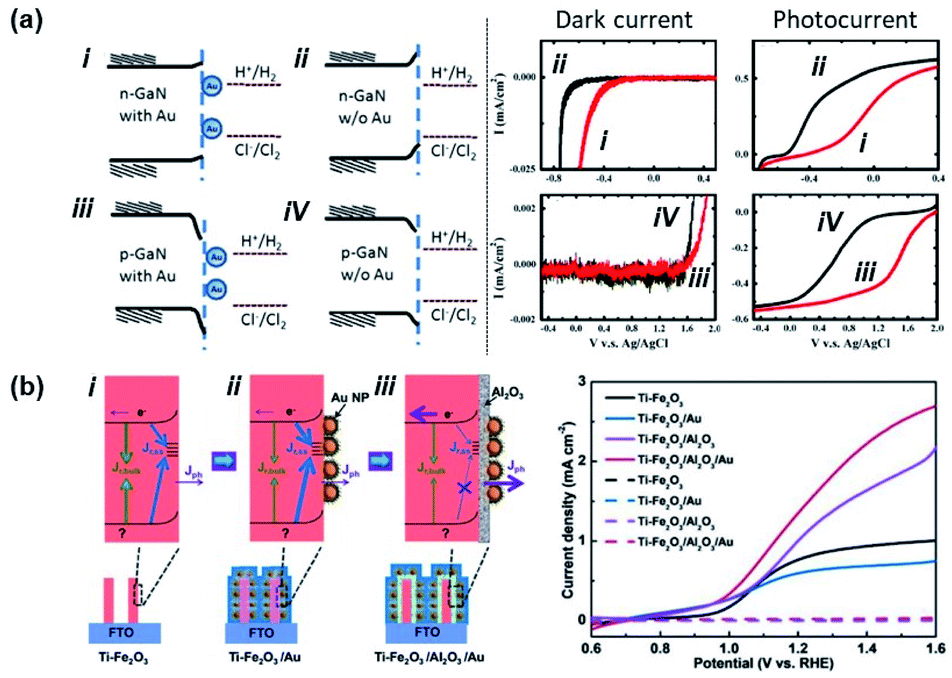 | ||
| Fig. 12 Fermi level pinning at a semiconductor–Au nanoparticle junction. (a) Band diagram and photoelectrochemical performance of Au nanoparticles interfaced with p/n-GaN. (Left) Band bending diagram of GaN in 1 M HCl electrolyte. (Right) Dark current and photocurrent from electrodes with (red line) and without (black line) Au NPs. Reproduced from ref. 135, copyright 2011, with permission from Elsevier. (b) (Left) Band bending diagram of Ti doped Fe2O3 nanorods (Ti–Fe2O3) (i) possessing interface states, (ii) with Au nanoparticles (Ti–Fe2O3/Au), and (iii) with an Al2O3 passivation layer and Au nanoparticles (Ti–Fe2O3/Al2O3/Au). (Right) Photocurrents of (i), (ii), and (iii). Reprinted from ref. 137, copyright 2018, with permission from Wiley-VCH. | ||
4.3 Au nanoparticle indirect contact formation methods
As introduced in Section 4.1, Au NPs can be brought into direct contact with the target substrate through PVD or solution-based methods. However, the degree of control over the particle size, shape and coverage offered by these methods is limited. In contrast, colloidal synthesis arguably provides a higher degree of control over the size and shape of Au NPs through additional tunable constraints associated with the use of ligands and capping agents. The contact between the metal and substrate, in this case, would not be direct due to the presence of ligands or capping agents on the NPs. However, the benefits of using well-controlled Au NP shapes could compensate for the potential weaknesses associated with the indirect contact formation. Au NP decoration methods that result in indirect contact with a photoelectrode surface are discussed below.If a photoelectrode and Au NPs are oppositely charged, the Au NPs are naturally attracted to the photoelectrode surface by coulombic attraction. Once the Au NPs arrive at the photoelectrode, the system achieves charge neutrality through charge transfer. Han et al. showed enhanced photoelectrochemical performances from CdS nanowires through the successful attachment of Au, Ag and Pt NPs. The NPs were prepared from a seed-mediated growth method using cetyltrimethylammonium bromide (CTAB), resulting in positive charges at the surface. Mercaptoacetic acid was adsorbed onto the surface of CdS nanowires by immersion to accumulate negative charge (Fig. 13a). After placing the CdS nanowires in the metal NP solution for several hours, the attractive coulombic forces led to the formation of CdS nanowires homogeneously decorated by metal NPs.139
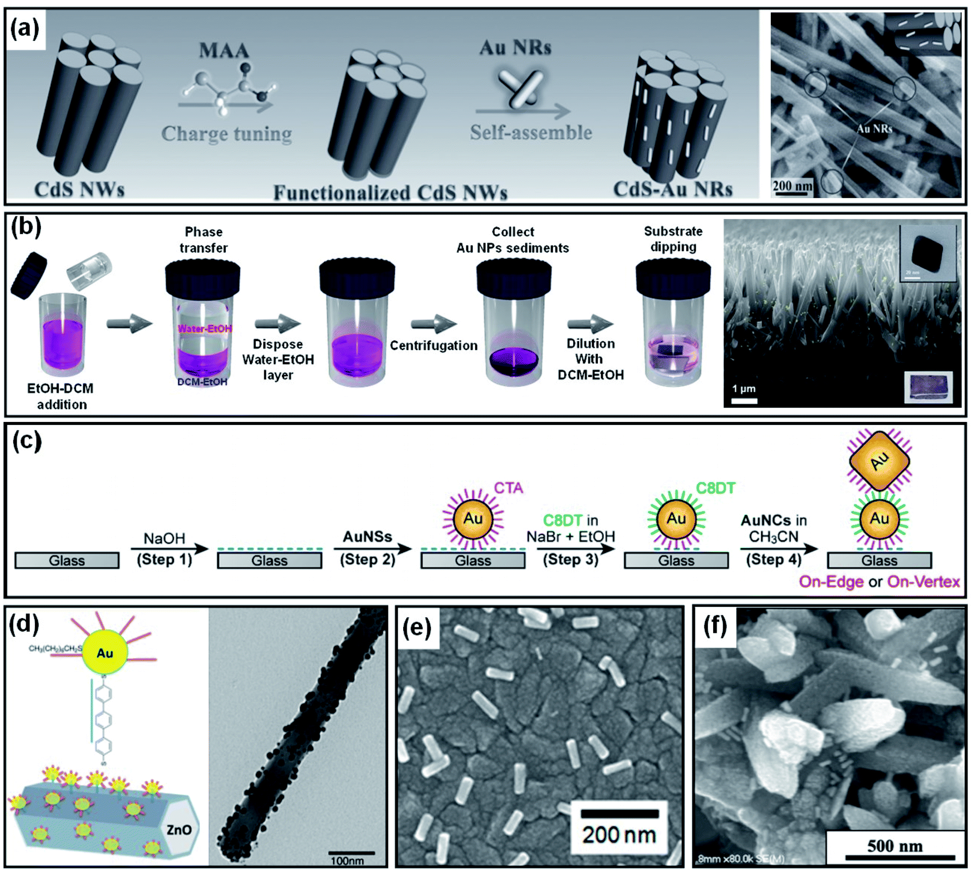 | ||
| Fig. 13 Methods to form indirect contact between a Au nanoparticle and photoactive semiconductor: (a) charge neutralization between the ligand and surface. Reprinted from ref. 139, copyright 2017, with permission from Wiley-VCH. (b) Ligand replacement. Reprinted from ref. 140, copyright 2018, with permission from the Royal Society of Chemistry. (c) Charge neutralization and post surface functionalization. Reprinted from ref. 141, copyright 2019, with permission from the American Chemical Society. (d) Surface functionalization. Reprinted from ref. 143, copyright 2015, with permission from the American Chemical Society. (e) Destabilization of the capping agent. Reprinted from ref. 144, copyright 2018, with permission from the American Chemical Society. (f) Dropcasting and heating. Reprinted from ref. 146, copyright 2020, with permission from the American Institute of Physics. | ||
A different method for homogeneous Au NP decoration is ligand exchange. Surface capping agents such as cetyltrimethylammonium bromide/chloride (CTAB/C) often used for seeded-growth can be replaced by another ligand through appropriate treatment. Specific functional groups are usually required to link Au NPs to the photoelectrode. The thiol (–SH) group enables selective gold–sulfur (Au–S) bonding. The hydroxide (–OH), carboxylate (–COO), or amino (–NH2) functional groups link with materials having (–O–) or (–NH–) terminal groups. Using these functional groups, Au NPs can be chemically bound to various photoelectrodes. For example, octahedral Au NPs capped with CTAB/C during synthesis were successfully attached to a TiO2 nanorod without aggregation through a ligand exchange reaction in dichloromethane using thiolated-polyethylene glycol (Fig. 13b).140 Forming a Au NP dimer is also possible through a solution process by exploiting charge neutralization and surface functionalization. M. Kim et al. demonstrated this process in a few steps (Fig. 13c). First, a CTAB/C-stabilized Au NP (positively charged) was anchored onto a NaOH treated glass substrate (negatively charged). To link the second Au NP onto the anchored NP, the anchored NP underwent a ligand exchange to a dithiol group (1,8-octanedithiol (C8DT)) which carries thiol groups on both sides of the ligand. To spatially restrict the linkage to the anchored NP, the surrounding NaOH was removed with acetonitrile. The second CTAB/C-stabilized Au NP was then attached to the anchored NP, resulting in the formation of a Au NP dimer.141 It is worth noting that the thiol group adheres well not only to Au but also to metal oxides.142 This allows a metal oxide substrate to be decorated with Au NPs by dithiol derivatives without the use of direct ligand exchange. After functionalization using dithiol, Au NPs can coat the desired metal oxide nanostructure. To improve spatial selectivity, the functional groups remaining on the unwanted regions of the substrate can be removed by heat treatment or ozone treatment (Fig. 13d).143
The quality of the contact between the Au NPs and the desired surface can be improved by removing the capping agents. For example, when Au nanorods synthesized with CTAB/C on a TiO2 substrate were treated with a hot water–ethanol mixture and annealed, the electrical contact between the two materials was found to improve (Fig. 13e).144 Similarly, Au NPs were pretreated with sulfuric acid before being drop-cast onto a TiO2 substrate to improve the contact quality.145 Another simple method is to spray a Au NP dispersed solution onto the desired nanostructure and heat the system for a certain period of time above 100 °C to induce complete water evaporation and physisorption (Fig. 13f).146
So far, we have discussed ways to bring capped Au NPs into contact with a desired surface and how to improve the contact. In the case where the NPs are not directly attached to the surface due to the presence of surface ligands, photocatalytic performances can be hindered through interface damping.
4.4 Chemical interface damping
Organic molecule adsorption is an inevitable consequence in the wet-chemical synthesis of Au NPs because capping agents are introduced to prevent aggregation and provide morphological control. Therefore, post-processes as mentioned in Section 4.3 are required to decorate Au NPs on the desired nanostructure. Sometimes, ligand exchange reactions are performed to provide functionality. These molecules act as small gaps that prevent direct contact of Au NPs with the desired surface, and are often considered to degrade the electrical performance. Recent findings have further shown that the adsorbed molecules can contribute to the plasmon damping mechanism separate from the commonly known radiative, bulk and surface damping processes. This damping contribution changes for Au NPs in different chemical environments and is referred to as chemical interface damping (CID). In short, the adsorbate presents an additional decay channel for the plasmon energy. As a consequence, the plasmon linewidth (Γ), which expresses the decay rate of the plasmon, can be summarized as a combination of four damping terms: bulk damping (Γbulk), radiation damping (Γrad) electron-surface damping (Γsurf) and CID (ΓCID).147| Γ = Γbulk + Γrad + Γsurf + ΓCID | (17) |
CID depends on multiple factors including charge transfer, NP size, induced dipole moment and resonance energy transfer. Foerster et al. investigated the dependence of the CID effect on NP size using Au nanorods functionalized with dodecanethiol (DDT).147 Effects of the CID were manifested as a decreased intensity, redshifted frequency, and broadened full width at half maximum (FWHM) in the LSPR. The authors showed that the CID effect became more dominant for smaller NPs and established that the CID is inversely proportional to the distance of electrons to the surface. Therefore, for very small ligand-functionalized Au NPs, the CID effect becomes dominant. Changing the chemical interface was further confirmed to modify the CID. Au nanorods functionalized with DDT and cetyltrimethylammonium bromide (CTAB) showed energy transfer efficiencies to the interface of 46% and 30%, respectively. The difference was found to arise from the different types of contact: covalent bonding (DDT) vs. physisorption (CTAB). This result indicates that the CID effect is highly dependent on the molecular structure and bonding at the Au NP surface. In fact, further studies showed that CID can be different even for two chemical isomers with the same molecular size. This was attributed to a difference in induced surface dipole moments.148 The lengths and types of the molecule are also relevant. The FWHM of the LSPR was not observed to change in the case of citrate capped Au NPs.149 But in the case of molecules with a thiol functional group, the FWHM was found to increase in proportion to the carbon length.150 The shape of the Au NPs was also found to be essential. For example, a sharp tip from a Au bipyramid was shown to produce stronger interface damping than a conventional Au NP.149 For more details on CID, readers can refer to the latest review.151
5. Boosting the photoelectrochemical water splitting reaction: the key role of the interface
This section introduces the various material systems used in plasmonic photoelectrochemical water splitting, focusing on the key role of the Au NPs. To choose the appropriate photoelectrode material, one must first carefully consider the position of the semiconductor band edge, the redox potential of water, and the Fermi level of the Au NPs. The alignment of these energy levels determines whether the reaction can take place or be efficient.78 It is assumed that the Fermi levels of the Au and the semiconductor line up with the redox level of water, which remains fixed since it presents a far larger number of available energy states compared to the other two. For simplicity, the corrosion potential of the photoelectrode is not considered here. The equilibration of charges between water and a semiconductor gives rise to band bending when the two are in contact, in a manner similar to the formation of the Schottky barrier for metal–semiconductor junctions. To allow for spontaneous charge exchange between water and the semiconductor, the Fermi level position for the photoanode and photocathode must satisfy EF,semi > ϕ0(H2O/O2) and EF,semi < ϕ0(H+/H2), respectively.88 If these two conditions are met, then introducing a Au NP can further promote the reaction efficiency by serving as a catalyst through the reduction of the recombination rate and improvement of the interfacial kinetics.152,153 The plasmonic effect of the Au NP is particularly well suited for improving the reaction at the photoanode due to the inherently slow kinetics of the OER.154 The band alignments of Au and 50 well-adopted photoactive water splitting semiconductors are depicted in Fig. 14 with respect to the redox potentials of water. The materials are displayed in descending order of valence band edge position from left to right. Among these, we narrow our discussion to a few popular semiconductors that have shown promise in enhanced water splitting with Au NPs.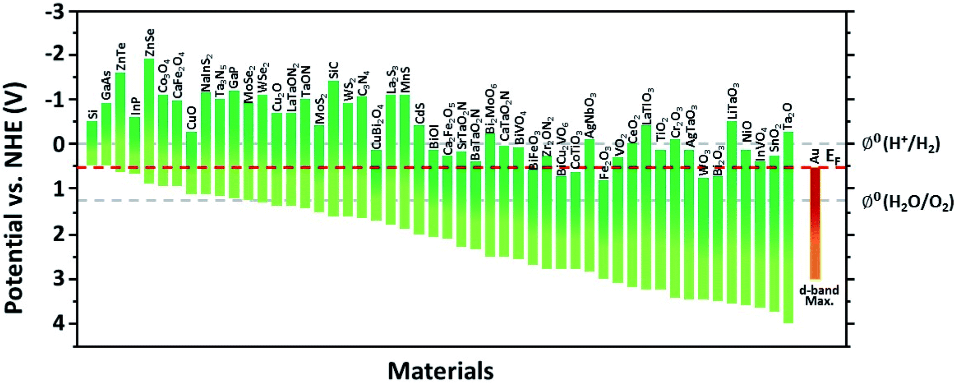 | ||
| Fig. 14 Band energies of semiconductors and the Fermi level of Au with a d-band maximum between the water redox levels. 50 widely used semiconductors are selected and displayed in descending order of valence band edge position from left to right. | ||
BiVO4 (BVO) is a promising photoanode material for photoelectrochemical water splitting because it displays a valence band position and bandgap well-suited for visible light absorption.155 Nevertheless, BVO based photoanodes have shown photoelectrochemical performances much poorer than theoretical predictions.156 This is largely due to charge recombination caused by the short diffusion length of the charge carriers and inefficient charge carrier separation.157 To improve the performance, Lee et al. introduced shape-controlled (octahedral and hemispherical) plasmonic Au NPs to the BVO photoanode.158 The authors investigated the photoactivity of the Au NP-decorated photoanode and reported an enhancement in the water splitting performance. Octahedral Au NPs were synthesized from seed-mediated growth and hemispherical Au NPs were formed from a PVD method. The photoelectrochemical properties of the photoanode with and without different shape Au NPs were measured in a phosphate buffer solution with a 0.1 M sodium sulphite hole scavenger. The authors found that the octahedral Au NP-decorated BiVO4 photoanode achieved a photocurrent density of 2.4 mA cm−2 at 1.23 V vs. RHE, which was three times higher than that of undecorated BiVO4. The main enhancement mechanism was proposed to originate from the combination of HCI and PIRET (Fig. 15a). Octahedral Au NPs were found to assist light absorption at the lower energy end of the bandgap enabled by the LSPR, and excite hot electrons across the Schottky barrier into the conduction band of BVO. The authors also found that PIRET can contribute to the enhancement because of the overlap between the absorption band of BVO and LSPR spectrum of the octahedral Au NPs, permitting the two materials to optically resonate together. Furthermore, an increase in field intensity near the sharp edges of the Au NP was proposed to induce a dipole near the semiconductor interface, resulting in a large increase in the generation rate of electron–hole pairs. As this effect is unique to the octahedral Au NP, the BVO photoanode decorated with octahedral Au NPs exhibited a higher photocurrent density compared to the case with hemispherical Au NPs, and a substantially higher improvement compared to the undecorated case. These mechanisms were clarified by comparing the IPCE profiles of the undecorated and octahedral Au NP-decorated BVO as shown in Fig. 15b. Observations of the IPCE enhancement in the off-resonance frequency and the intense local fields generated by the pointed vertices of octahedral shape were strong indicators of the PIRET mechanism.
 | ||
| Fig. 15 (a) Energy band diagram of the BiVO4 photoanode with an octahedral Au NP that shows the HCI (DET) and PRET mechanisms. (b) IPCE spectra of BiVO4 and octahedral Au NP/BiVO4 photoanodes at 1.23 V vs. RHE. (a) and (b) are reprinted from ref. 158, copyright 2017, with permission from Wiley-VCH. (c) Schematic of the energy band diagram for a Au NP/TiO2 nanotube array-photoelectrode under visible light illumination that shows the mechanism for the hot electron mediated OER. Reprinted from ref. 163, copyright 2018, with permission from the Royal Society of Chemistry. (d) Energy band diagram of the Au–MoS2 heterostructure with formation of a Schottky barrier. (e) Calculated electric field intensity as a function of wavelength. The inset shows the electric field distribution at 1405 nm. (d) and (e) are reprinted from ref. 168, copyright 2019, with permission from the Royal Society of Chemistry. (f) Possible mechanisms for the HER in a Au@CeO2 core–shell photocatalyst under visible light illumination. Reprinted from ref. 171, copyright 2021, with permission from Elsevier. | ||
Kim et al. investigated the photoelectrochemical properties of a Mo-doped BiVO4 (Mo:BiVO4) photoanode using patterned Au nanospheres where the improved performance was attributed to the PIRET mechanism.159 To generate hot spots across the photoanode area, the authors formed a dense hexagonal array of Au NPs on the photoanode by electrodeposition. The Au NP sizes were also modulated to find the optimum structure. Through transient absorption and time-correlated single photon counting studies, the authors showed an increase in the lifetime of electrons and holes, corresponding to the PIRET effect. The Mo:BVO photoanode with patterned Au nanospheres also showed a 2.2-fold higher photocurrent density compared to a bare Mo:BiVO4 photoanode. These results demonstrated that the plasmonic effect not only expands the light absorption over a broad ultraviolet–visible light region but also enhances the charge transfer and transport efficiencies.
Ghobadi et al. also showed strong improvements in the photocurrent for Au capped nanoporous BVO photoanodes.160 Au caps were selectively deposited on the top of the BVO nanostructures by vacuum-depositing Au at an oblique angle. The photoelectrochemical measurements were carried out using a phosphate-buffered saline (pH 7) solution. The photocurrent density was boosted from 190 μA cm−2 for bare BiVO4 to 295 μA cm−2 for Au–BiVO4. With the Au cap, photogenerated holes from the BVO valence band and hot holes created by the Au nanounits were proposed to contribute to the photocurrent enhancement. Multiple benefits of Au nanounits were outlined as follows: (i) increase in light absorption of the BVO photoanode, (ii) generation of hot holes, which can participate in the direct oxidation of water, (iii) acceleration of reaction as co-catalysts by mediating the electron transfer from the valence band of BiVO4 to the electrolyte, and (iv) generation of Fabry–Perot (FP) modes for above-bandgap photons (λ < 520 nm), and LSPR-induced activation of hot electron injection with sub-bandgap photons (λ > 520 nm). Au-capped nanoporous BiVO4 with these superior photoelectrochemical capabilities was coupled with a water oxidation catalyst (CoFe-Prussian blue analog) to enhance the electron transfer dynamics and maximize the photoelectrochemical water splitting performance.
Choi and co-workers reported enhanced PEC properties of hematite and BVO semiconductors with 2D arranged globular Au NPs. The PEC water splitting performance was characterized in a 1 M KOH electrolyte with Pt wire as a counter electrode and Hg/HgO as a reference electrode. The photocurrent density from a Au array/Fe2O3 was 1.07 mA cm−2 at 1.23 V vs. RHE, which was 3.3-fold higher than that from a bare Fe2O3 photoanode (0.31 mA cm−2). To evaluate the charge transfer and charge transport ability, the photocurrent density was measured with a hole scavenger. Charge carrier recombination was found to be suppressed in PEC cells through PIRET.161
TiO2 is another popular semiconductor material for water splitting studies, and is the oldest, being the material that jumpstarted the field of water splitting. However, in its bare form, it is unable to absorb visible light due to its large bandgap, which keeps it from harnessing the strongest irradiance region of the solar spectrum.162 To this end, there have been concerted efforts to enhance its photoelectrochemical performance through the use of plasmonic NPs. Moon et al. reported on the improved photocatalytic activity of TiO2 nanotube arrays decorated with citrate-stabilized Au NPs of various sizes.163 They tested the photoelectrochemical performance under visible light (λ > 415 nm) in a conventional three-electrode system. A quartz cell filled with 1 M KOH electrolyte was used for the measurement. The electrochemically dormant TiO2 nanotube arrays were activated with Au NPs, where attachment of smaller Au NPs produced the highest photocurrent density of 0.14 mA cm−2. The working principle is shown in Fig. 15c. Hot electrons and hot holes are excited in Au NPs by LSPR relaxation under visible light. It is clear that a low barrier height is beneficial for easier charge transfer into the semiconductor. The authors showed through conductive atomic force microscopy that the Schottky barrier height was lower for the smaller Au NPs. These results prove that the Au NP size plays an important role in shaping not only the optical properties at the interface but also the electronic properties.
The influence of the Au NP shape on the photoelectrochemical water splitting properties of the TiO2 photoanode was also explored by C. W. Moon et al.164 Various shapes of Au NPs including citrate synthesized quasi-spherical Au NPs, seed-grown octahedral Au NPs, and vacuum-deposited hemispherical Au NPs were prepared on a TiO2 thin film photoanode. For the photoelectrochemical characterization, the authors used 1 M NaOH solution as an electrolyte, Pt wire as a counter electrode, and a Ag/AgCl (saturated KCl) electrode as a reference electrode. The attachment of spherical Au NPs to TiO2 decreased the photocurrent density, while the attachment of octahedral Au NPs led to a more than two-fold increase in photocurrent from 76 μA cm−2 to 170 μA cm−2. Two laser sources at 532 and 405 nm were used to investigate intraband and interband generated photocurrents, respectively. For 532 nm excitation, the photoanode with hemispherical Au NPs showed the highest photocurrent density, while for 405 nm excitation, the photoanode with octahedral Au NPs exhibited a superior photocurrent density. The authors explained that the intense local field from the sharp vertices of the octahedral Au NPs facilitates hole transfer to the water–Au interface for oxygen evolution. They also explored the effect of light shading from Au NPs that may be deteriorative to photocatalytic activity. They controlled the coverage of Au NPs to minimize the shading effect, which may degrade the photocatalytic activity.
To better understand the enhancement mechanisms in Au NP decorated TiO2 photocatalysts, Asapu et al. experimentally disentangled the near-field mechanism and charge transfer process.165 The authors selectively suppressed or induced the charge transfer and field enhancement effect by introducing a spacer shell on the Au NPs. The thickness and conductivity of the shell were controlled to separate the Au NP from the TiO2 surface and enable electron transfer, respectively, while surface-enhanced Raman spectroscopic (SERS) measurements were employed to quantify the effect of the near-field enhancement. As the shell thickness increased, the near-field effect was found to gradually decrease, which was supported through measurements of the SERS enhancement factor and electromagnetic field enhancement simulations. The study showed that the HCI mechanism was rather limited in the absence of the near-field enhancement effect. Furthermore, it was shown that the HCI no longer occurs when the Au NP is encapsulated with an ultrathin insulating layer, in which case only the near-field effect can be attributed to the photocatalytic reaction rate enhancement. Regardless of the conductivity of the shell, the reaction rate degraded with increasing shell thickness. The authors concluded that the distance between the Au NP and TiO2 is more critical than the conductivity of the shell in HCI.
Adding cocatalysts or catalytic sensitizers to the Au NP–TiO2 photoanode is a strategy for synergistically achieving additional enhancements in the photoelectrochemical performance. Okazaki et al. studied plasmonic photoelectrochemical water oxidation with a site-selective CoOx deposited Au/TiO2 thin film.166 Au NPs were formed by coalescence from a Au film. The optimized CoOx/Au/TiO2 photoanode demonstrated a ∼3 times higher photocurrent density compared to the unsensitized Au/TiO2 photoanode due to the synergetic effect between Au NPs and the CoOx, which is a cocatalyst and a catalytic sensitizer for water oxidation with TiO2.167 However, excess deposition of CoOx was found to reduce the active surface area for water oxidation and bury the interface between TiO2 and Au, interrupting the movement of holes from the active interface between Au and TiO2 to the surface of CoOx and resulting in poorer water oxidation activity.
2D transition metal dichalcogenides (TMDs) have also been receiving increased attention as possible candidates for water splitting, where the bandgap energy can be varied by controlling the number of stacked TMD layers. This is a powerful ability that allows one to easily engineer the bandgap to satisfy the optical and electronic demands of photoelectrochemical water splitting. Ali et al. examined the photoelectrochemical water splitting reaction of Au NPs/Au nanorods on MoS2 nanosheets (Fig. 15d and e).168 The MoS2 nanosheets were engineered to support a bandgap of 1.3 eV, which can harness photons from the UV to the NIR range. Au NPs were formed on MoS2 nanosheets by reducing Au ions with ascorbic acid. Au nanorods were synthesized by a seeded-growth method and were attached to the MoS2 nanosheets by gentle mixing. To measure the photoelectrochemical water splitting, a buffer solution of 0.1 M KH2PO4 (pH 7) was used. The authors found that the MoS2 decorated with Au nanorods and Au NPs showed 2 times and 3.5 times higher OER efficiency in the visible–infrared region than the bare MoS2, respectively, where the improved photoactivity was attributed to multiple factors including a larger number of reaction sites, the plasmon-induced HCI effect and local field enhancements (LEMF).
While many of the examples discussed above report water oxidation performances at the photoanode, water reduction at the photocathode for the production of hydrogen is also an active area of research that benefits tremendously from plasmonics. Various architectures that rationally combine distinct semiconductors and plasmonic metals to synergistically boost the HER efficiency have been proposed. As an example, an improvement in the HER performance with a CdS–Au/MoS2 core–shell heteronanostructure photocathode was reported by Chava and co-workers.169 Au NPs were synthesized by citrate reduction and the CdS nanorods were prepared by a solvothermal method. The CdS–Au/MoS2 hybrid nanostructure was prepared by mixing the CdS nanorods in a Au colloidal solution, after which MoS2 precursors were added. The mixture was allowed to react in an autoclave, resulting in the formation of MoS2 nanosheets on the Au NP-decorated CdS nanorod. For the measurement of photocatalytic hydrogen production, 10 mg of photocatalytic powder was suspended in 50 mL of aqueous solution with 10% lactic acid as a sacrificial reagent. The apparent quantum yield of the CdS–Au/MoS2 photocatalyst was calculated to be 27.85%. The hybrid nanorods demonstrated a 7 times higher H2 evolution rate (7.01 mmol g−1 h−1) and 5 times higher current density (32.67 μA cm−2) than bare CdS nanorods, which the authors explained was through the combined effects of increased carrier generation rate in the CdS due to LEMF, the facile electron transfer from CdS to MoS2 mediated by the Au NPs, and the abundance of catalytically active sites for H2 provided by the MoS2.
Shi and co-workers reported the photocatalytic properties of Au/CdSe nanocrystal clusters under visible-light. They synthesized the Au/CdSe nanocrystal cluster through an emulsion-based self-assembly approach. The photocatalytic hydrogen evolution activities were determined in Na2S/Na2SO3 aqueous solution under visible light (λ > 420 nm). The Au/CdSe nanocrystals with 7.2 nm Au NPs achieved a hydrogen evolution rate of 73 mmol gCdSe−1 h−1, which was 10 times higher than that of the bare CdSe nanocrystals (7.2 mmol gCdSe−1 h−1). The outstanding photocatalytic performance was found to derive from PRET between the Au NPs and the CdSe nanocrystals, which suppresses the bulk recombination and boosts the charge carrier generation in the semiconductor.170
Rare-earth semiconductors have also been known to exhibit attractive photocatalytic properties, prompting studies that combine them with plasmonic NPs for improved water splitting performances. Dao and co-workers investigated plasmonic Au@CeO2 core–shell photocatalysts for the HER (Fig. 15f).171 To evaluate the photocatalytic HER, 50 mg of the photocatalyst was dispersed in 50 mL of methanol (25%) solution as a sacrificial reagent. The Au@CeO2 core–shell photocatalysts demonstrated 10 times superior HER rates (4.05 μmol mg−1 h−1) than pure CeO2 (0.40 μmol mg−1 h−1) under visible light, and improved long-term stability. The Au@CeO2 core–shell photocatalyst achieved an apparent quantum yield of 19.46% at 550 nm, which is a much higher value compared to that of CeO2. These improvements were accounted for by multiple mechanisms which we outline here. (i) The strong plasmonic near-field from the Au NP at resonance penetrates into the CeO2 shell, greatly increasing the electron–hole pair generation rate. This is the LEMF effect. (ii) The HCI effect also plays an important role. The excited LSPR decays through Landau damping, exciting hot electrons from the d-band (ground state) that cross over the Schottky barrier at the interface of the core–shell structure and into conduction bands (Ce3+ and Ce4+) of CeO2, which increases the free electron density in the CeO2 shell.172 The accumulated hot electrons in the CeO2 conduction band can drive the conversion of H+ ions to H2 at the shell surface. (iii) PIRET can also be a contributing mechanism since the LSPR and ceria absorption spectra overlap. The PIRET helps the CeO2 harvest electron–hole pairs under visible light with lower energy states compared to the conduction band and promotes electrons in the valence band of CeO2 into the conduction band of CeO2 (Ce3+). (iv) The enrichment of Ce3+ in the CeO2 shell also affects the performance. This causes the plasmonically excited electrons to populate the Ce3+ conduction band, and also allows electron hopping from Ce3+ states (4f1) to Ce4+ states. The high concentration of electrons is then used to drive the HER.
As can be witnessed, extensive research efforts have been dedicated to understanding and designing photoelectrochemical water splitting systems with a combination of plasmonic NPs and various semiconductor systems. According to the ‘Web of Science’, the number of citations from reports including the keywords ‘solar’ and ‘plasmon’ is progressively increasing, as shown in Fig. 16a. This trend proves the rising level of interest in the area of solar energy harvesting, and reflects the growing importance of the topic. It is well understood that efficient water splitting technology is key to achieving a clean and sustainable fuel that is consumable in many sectors of industry and technology (Fig. 16b). From the past three decades of scientific research, we now have a better understanding of the plasmonic interactions between Au NPs and photocatalytic systems that can help lead us toward devising more efficient and economical systems for hydrogen fuel generation.
 | ||
| Fig. 16 (a) Number of citations on publications with keywords ‘solar’ and ‘plasmon’, from the Web of Science. (b) Schematic of a hydrogen fuel society. | ||
6. Conclusion
Since the breakthrough discovery of the Honda–Fujishima effect in 1972, research activity on improving water splitting efficiencies to practical and economical levels has been rising in the face of accelerating climate change and exacerbating environmental pollution. Our renewed interest in and improved understanding of plasmonic systems and their decay mechanisms have greatly benefited this effort by introducing pathways for improving the water splitting performance beyond classical limits. Among the few plasmonic candidates, Au NPs are regarded as the champion nanomaterials for solar water splitting applications, because they are resistant to corrosion in solution, possess plasmonic resonance in the visible region unlike Ag and Al, and are easily preparable in various shapes, sizes, and dimensions.Over the past three decades, we have learned that Au NPs coupled with photoactive surfaces can bring forth a number of benefits through a variety of mechanisms. The plasmonic decay accompanying the LSPR excitation can mediate charge transfer from the NP to the coupled photoactive surface through hot carrier injection over the Schottky barrier, dipole–dipole coupling, tunneling, and wavefunction overlap, which we described in the initial sections. Also the strongly concentrated near-field intensity associated with the LSPR can be used to enhance the charge carrier generation rate in the photoactive material, leading to further improvements. These effects can be tuned by varying the shape, size and dimension of the NPs that allow one to selectively control the various mechanisms. Combined with the appropriate semiconductor material, the Au NP–photoactive material can be rationally designed to satisfy the optical and electronic demands of the envisioned water splitting system.
In the last section, we selectively reviewed recent research efforts that combine Au NPs with various semiconductor materials. The common strategy was to use Au NPs to compensate for the electronic and optical limitations inherent in the semiconductors. The Au NPs were shown to increase the light absorption, boost the generation rate of charge carriers, facilitate charge transfer, and improve charge separation, resulting in enhanced photoelectrochemical water splitting performance. While a huge variety of different semiconductors combined with Au NPs have been studied, the phase space still remains vast. There are still plenty of opportunities to find improved designs and material combinations that offer dramatic improvements in performance.
Despite the wealth of accumulated knowledge, we still have not witnessed plasmonic photoelectrochemical water splitting reaching mainstream use. In order to achieve a self-sustainable hydrogen cycle, water splitting must be economically feasible, which can be achieved by either lowering the cost of the materials and production, or by achieving further improvements in the water splitting efficiency. Challenges still remain in these two areas. Most notably, Au is inherently expensive and its price is very sensitive to market fluctuations. Therefore, developing cheaper plasmonic materials that exhibit low optical loss and high stability is necessary. In this regard, plasmonic metal alloys173 and metal nitrides174 offer promising solutions. Scalable fabrication techniques for plasmonic NPs with optimized shapes, and improved NP–semiconductor designs that efficiently harness the beneficial effects of the plasmonic NPs must also be realized. Furthermore, research into extending the absorption bandwidth of light into the NIR region can also lead to improvements in the photoelectrochemical conversion efficiency. As many of the concepts in this review are general to coupled plasmonic NP–semiconductor systems, we hope that the readers will also find them useful in other solar harvesting systems such as photovoltaics, photosynthesis and photothermal devices.
Conflicts of interest
There are no conflicts to declare.Acknowledgements
C. W. M., and M.-J. C. contributed equally to this work. The authors acknowledge financial support from a National Research Foundation of Korea (NRF) grant funded by the Korean government (MIST) (NRF-2017R1A5A1015365, 2019R1C1C1002802, 2021R1A2B5B03001851, and 2021M3D1A2039641).References
- C. Acar and I. Dincer, J. Clean. Pro., 2019, 218, 835–849 CrossRef CAS.
- A. M. Abdalla, S. Hossain, O. B. Nisfindy, A. T. Azad, M. Dawood and A. K. Azad, Energy Convers. Manag., 2018, 165, 602–627 CrossRef CAS.
- M. G. Walter, E. L. Warren, J. R. McKone, S. W. Boettcher, Q. Mi, E. A. Santori and N. S. Lewis, Chem. Rev., 2010, 110, 6446–6473 CrossRef CAS PubMed.
- Y. Lin, G. Yuan, R. Liu, S. Zhou, S. W. Sheehan and D. Wang, Chem. Phys. Lett., 2011, 507, 209–215 CrossRef CAS.
- L. J. Minggu, W. R. W. Daud and M. B. Kassim, Int. J. Hydrogen Energy, 2010, 35, 5233–5244 CrossRef CAS.
- M.-J. Choi, T. L. Kim, J. K. Kim, T. H. Lee, S. A. Lee, C. Kim, K. Hong, C. W. Bark, K.-T. Ko and H. W. Jang, Nano Lett., 2020, 20, 8040–8045 CrossRef CAS PubMed.
- S. A. Lee, I. J. Park, J. W. Yang, J. Park, T. H. Lee, C. Kim, J. Moon, J. Y. Kim and H. W. Jang, Cell Rep. Phys. Sci., 2020, 1, 100219 CrossRef CAS.
- T. H. Lee, S. A. Lee, H. Park, M.-J. Choi, D. Lee and H. W. Jang, ACS Appl. Energy Mater., 2020, 3, 1634–1643 CrossRef CAS.
- T. L. Kim, M.-J. Choi, T. H. Lee, W. Sohn and H. W. Jang, Nano Lett., 2019, 19, 5897–5903 CrossRef CAS PubMed.
- W. L. Barnes, A. Dereux and T. W. Ebbesen, Nature, 2003, 424, 824–830 CrossRef CAS PubMed.
- S. A. Maier, Plasmonics: Fundamentals and Applications, Springer Science & Business Media, 2007 Search PubMed.
- J. Li, S. K. Cushing, P. Zheng, F. Meng, D. Chu and N. Wu, Nat. Commun., 2013, 4, 1–8 CAS.
- C. W. Moon, G. Kim and J. K. Hyun, J. Mater. Chem. C, 2021, 9, 1764–1771 RSC.
- A. Kristensen, J. K. Yang, S. I. Bozhevolnyi, S. Link, P. Nordlander, N. J. Halas and N. A. Mortensen, Nat. Rev. Mater., 2016, 2, 1–14 Search PubMed.
- G. Zhao, H. Kozuka and T. Yoko, Thin Solid Films, 1996, 277, 147–154 CrossRef CAS.
- S. K. Cushing, A. D. Bristow and N. Wu, Phys. Chem. Chem. Phys., 2015, 17, 30013–30022 RSC.
- C. Clavero, Nat. Photonics, 2014, 8, 95–103 CrossRef CAS.
- K. A. Willets and R. P. Van Duyne, Annu. Rev. Phys. Chem., 2007, 58, 267–297 CrossRef CAS PubMed.
- J. N. Anker, W. P. Hall, O. Lyandres, N. C. Shah, J. Zhao and R. P. Van Duyne, Nanoscience and Technology: A Collection of Reviews from Nature Journals, 2010, pp. 308–319 Search PubMed.
- B. Lee, I.-M. Lee, S. Kim, D.-H. Oh and L. Hesselink, J. Mod. Opt., 2010, 57, 1479–1497 CrossRef.
- C. F. Bohren and D. R. Huffman, Absorption and Scattering of Light by Small Particles, John Wiley & Sons., 2008 Search PubMed.
- K. L. Kelly, E. Coronado, L. L. Zhao and G. C. Schatz, J. Phys. Chem. B, 2003, 107, 668–677 CrossRef CAS.
- E. Petryayeva and U. J. Krull, Anal. Chim. Acta, 2011, 706, 8–24 CrossRef CAS PubMed.
- A. S. Kumbhar, M. K. Kinnan and G. Chumanov, J. Am. Chem. Soc., 2005, 127, 12444–12445 CrossRef CAS PubMed.
- S. A. Maier and H. A. Atwater, J. Appl. Phys., 2005, 98, 10 CrossRef.
- G. Mie, Ann. Phys., 1908, 330, 377–445 CrossRef.
- P. K. Jain, K. S. Lee, I. H. El-Sayed and M. A. El-Sayed, J. Phys. Chem. B, 2006, 110, 7238–7248 CrossRef CAS PubMed.
- Z. Wei, L. Rosa, K. Wang, M. Endo, S. Juodkazis, B. Ohtani and E. Kowalska, Appl. Cata. B, 2017, 206, 393–405 CrossRef CAS PubMed.
- L. M. Liz-Marzán, Langmuir, 2006, 22, 32–41 CrossRef PubMed.
- H. Ditlbacher, J. Krenn, B. Lamprecht, A. Leitner and F. Aussenegg, Opt. Lett., 2000, 25, 563–565 CrossRef CAS PubMed.
- C. J. Murphy, T. K. Sau, A. M. Gole, C. J. Orendorff, J. Gao, L. Gou, S. E. Hunyadi and T. Li, J. Phys. Chem. B, 2005, 109, 13857–13870 CrossRef CAS PubMed.
- J. Cao, T. Sun and K. T. Grattan, Sens. Actuators, B, 2014, 195, 332–351 CrossRef CAS.
- V. Myroshnychenko, J. Rodríguez-Fernández, I. Pastoriza-Santos, A. M. Funston, C. Novo, P. Mulvaney, L. M. Liz-Marzán and F. J. G. De Abajo, Chem. Soc. Rev., 2008, 37, 1792–1805 RSC.
- W. Gotschy, K. Vonmetz, A. Leitner and F. Aussenegg, Appl. Phys. B, 1996, 63, 381–384 CrossRef CAS.
- E. Prodan, C. Radloff, N. J. Halas and P. Nordlander, Science, 2003, 302, 419–422 CrossRef CAS PubMed.
- X. Lu, M. Rycenga, S. E. Skrabalak, B. Wiley and Y. Xia, Annu. Rev. Phys. Chem., 2009, 60, 167–192 CrossRef CAS PubMed.
- A. Das, K. Kumar and A. Dhawan, RSC Adv., 2021, 11, 8096–8106 RSC.
- H. B. Jeon, P. V. Tsalu and J. W. Ha, Sci. Rep., 2019, 9, 1–8 Search PubMed.
- T. Klar, M. Perner, S. Grosse, G. Von Plessen, W. Spirkl and J. Feldmann, Phys. Rev. Lett., 1998, 80, 4249 CrossRef CAS.
- L. Yuan, Z. Geng, J. Xu, F. Guo and C. Han, Adv. Funct. Mater., 2021, 31, 2101103 CrossRef CAS.
- K. Matsuzaki, H.-W. Liu, S. Götzinger and V. Sandoghdar, ACS Photonics, 2021, 8, 1508–1521 CrossRef CAS.
- C. Sönnichsen, T. Franzl, T. Wilk, G. von Plessen, J. Feldmann, O. Wilson and P. Mulvaney, Phys. Rev. Lett., 2002, 88, 077402 CrossRef PubMed.
- T. Hertel, E. Knoesel, M. Wolf and G. Ertl, Phys. Rev. Lett., 1996, 76, 535 CrossRef CAS PubMed.
- F. Ladstädter, U. Hohenester, P. Puschnig and C. Ambrosch-Draxl, Phys. Rev. B: Condens. Matter Mater. Phys., 2004, 70, 235125 CrossRef.
- M. Lisowski, P. Loukakos, U. Bovensiepen, J. Stähler, C. Gahl and M. Wolf, Appl. Phys. A, 2004, 78, 165–176 CrossRef CAS.
- C. Voisin, N. Del Fatti, D. Christofilos and F. Vallée, J. Phys. Chem. B, 2001, 105, 2264–2280 CrossRef CAS.
- M. I. Litter, Appl. Catal. B, 1999, 23, 89–114 CrossRef CAS.
- H. Zhu, X. Chen, Z. Zheng, X. Ke, E. Jaatinen, J. Zhao, C. Guo, T. Xie and D. Wang, Chem. Commun., 2009, 7524–7526 RSC.
- A. L. Linsebigler, G. Lu and J. T. Yates Jr, Chem. Rev., 1995, 95, 735–758 CrossRef CAS.
- G. Baffou and R. Quidant, Laser Photon. Rev., 2013, 7, 171–187 CrossRef CAS.
- M. L. Brongersma, N. J. Halas and P. Nordlander, Nat. Nanotechnol., 2015, 10, 25–34 CrossRef CAS PubMed.
- L. Mascaretti, A. Dutta, Š. Kment, V. M. Shalaev, A. Boltasseva, R. Zbořil and A. Naldoni, Adv. Mater., 2019, 31, 1805513 CrossRef PubMed.
- K. Wu, J. Chen, J. R. McBride and T. Lian, Science, 2015, 349, 632–635 CrossRef CAS PubMed.
- R. Long and O. V. Prezhdo, J. Am. Chem. Soc., 2014, 136, 4343–4354 CrossRef CAS PubMed.
- L. Du, A. Furube, K. Yamamoto, K. Hara, R. Katoh and M. Tachiya, J. Phys. Chem. C, 2009, 113, 6454–6462 CrossRef CAS.
- A. Furube, L. Du, K. Hara, R. Katoh and M. Tachiya, J. Am. Chem. Soc., 2007, 129, 14852–14853 CrossRef CAS PubMed.
- T. Förster, Ann. Phys., 1948, 437, 55–75 CrossRef.
- J. Li, S. K. Cushing, F. Meng, T. R. Senty, A. D. Bristow and N. Wu, Nat. Photonics, 2015, 9, 601–607 CrossRef CAS.
- S. K. Cushing, J. Li, F. Meng, T. R. Senty, S. Suri, M. Zhi, M. Li, A. D. Bristow and N. Wu, J. Am. Chem. Soc., 2012, 134, 15033–15041 CrossRef CAS PubMed.
- T. Hisatomi, K. Takanabe and K. Domen, Catal. Lett., 2015, 145, 95–108 CrossRef CAS.
- R. Sundararaman, P. Narang, A. S. Jermyn, W. A. Goddard III and H. A. Atwater, Nat. Commun., 2014, 5, 1–8 Search PubMed.
- A. O. Govorov, H. Zhang, H. V. Demir and Y. K. Gun’ko, Nano Today, 2014, 9, 85–101 CrossRef CAS.
- S. F. Hung, F. X. Xiao, Y. Y. Hsu, N. T. Suen, H. B. Yang, H. M. Chen and B. Liu, Adv. Energy Mater., 2016, 6, 1501339 CrossRef.
- A. M. Brown, R. Sundararaman, P. Narang, W. A. Goddard III and H. A. Atwater, ACS Nano, 2016, 10, 957–966 CrossRef CAS PubMed.
- A. Manjavacas, J. G. Liu, V. Kulkarni and P. Nordlander, ACS Nano, 2014, 8, 7630–7638 CrossRef CAS PubMed.
- J. Zhao, S. C. Nguyen, R. Ye, B. Ye, H. Weller, G. A. Somorjai, A. P. Alivisatos and F. D. Toste, ACS Cent. Sci., 2017, 3, 482–488 CrossRef CAS PubMed.
- W.-T. Wu, C.-H. Chen, C.-Y. Chiang and L.-K. Chau, Sensors, 2018, 18, 1759 CrossRef PubMed.
- C. Lee, Y. Park and J. Y. Park, RSC Adv., 2019, 9, 18371–18376 RSC.
- C. Zhan, M. Moskovits and Z.-Q. Tian, Matter, 2020, 3, 42–56 CrossRef.
- H. Bai, P. Guan, K. Qu, W. Fan, F. Wang, D. Xu, J. Ding and W. Shi, Int. J. Hydrogen Energy, 2019, 44, 28184–28193 CrossRef CAS.
- L. Wang, H. Hu, N. T. Nguyen, Y. Zhang, P. Schmuki and Y. Bi, Nano Energy, 2017, 35, 171–178 CrossRef CAS.
- W. Shockley and H. J. Queisser, J. Appl. Phys., 1961, 32, 510–519 CrossRef CAS.
- S. Rühle, Solar Energy, 2016, 130, 139–147 CrossRef.
- A. Fujishima and K. Honda, Nature, 1972, 238, 37–38 CrossRef CAS PubMed.
- J. R. Bolton, S. J. Strickler and J. S. Connolly, Nature, 1985, 316, 495–500 CrossRef CAS.
- H. Döscher, J. Geisz, T. Deutsch and J. Turner, Energy Environ. Sci., 2014, 7, 2951–2956 RSC.
- T. J. Jacobsson, V. Fjällström, M. Edoff and T. Edvinsson, Sol. Energy Mater. Sol. Cells, 2015, 138, 86–95 CrossRef CAS.
- L.-J. Guo, J.-W. Luo, T. He, S.-H. Wei and S.-S. Li, Phys. Rev. Appl., 2018, 10, 064059 CrossRef CAS.
- K. T. Fountaine, H. J. Lewerenz and H. A. Atwater, Nat. Commun., 2016, 7, 1–9 Search PubMed.
- F. Guo, N. Li, F. W. Fecher, N. Gasparini, C. O. R. Quiroz, C. Bronnbauer, Y. Hou, V. V. Radmilović, V. R. Radmilović and E. Spiecker, Nat. Commun., 2015, 6, 1–9 Search PubMed.
- Y. Yan, R. W. Crisp, J. Gu, B. D. Chernomordik, G. F. Pach, A. R. Marshall, J. A. Turner and M. C. Beard, Nat. Energy, 2017, 2, 1–7 Search PubMed.
- J. Kong, X. Wu, X. Wang, M. J. Naughton and K. Kempa, Phys. Rev. Mater., 2019, 3, 065201 CrossRef CAS.
- P. Christopher, H. Xin, A. Marimuthu and S. Linic, Nat. Mater., 2012, 11, 1044–1050 CrossRef CAS PubMed.
- Y. Kim, J. G. Smith and P. K. Jain, Nat. Chem., 2018, 10, 763–769 CrossRef CAS PubMed.
- J. A. Schuller, E. S. Barnard, W. Cai, Y. C. Jun, J. S. White and M. L. Brongersma, Nat. Mater., 2010, 9, 193–204 CrossRef CAS PubMed.
- Y. Xu, T. Gong and J. N. Munday, Sci. Rep., 2015, 5, 1–9 Search PubMed.
- A. O. Govorov, H. Zhang and Y. K. Gun’ko, J. Phys. Chem. C, 2013, 117, 16616–16631 CrossRef CAS.
- X. Zhang, Y. L. Chen, R.-S. Liu and D. P. Tsai, Rep. Prog. Phys., 2013, 76, 046401 CrossRef PubMed.
- J. B. Khurgin, Nanophotonics, 2020, 9, 453–471 CAS.
- A. M. Elsharif, Chem. Phys. Lett., 2018, 691, 224–230 CrossRef CAS.
- G. V. Hartland, L. V. Besteiro, P. Johns and A. O. Govorov, ACS Energy Lett, 2017, 2, 1641–1653 CrossRef CAS.
- X. T. Kong, Z. Wang and A. O. Govorov, Adv. Opt. Mater., 2017, 5, 1600594 Search PubMed.
- S. K. Cushing, C.-J. Chen, C. L. Dong, X.-T. Kong, A. O. Govorov, R.-S. Liu and N. Wu, ACS Nano, 2018, 12, 7117–7126 CrossRef CAS PubMed.
- M. Moskovits, Science, 2011, 332, 676–677 CrossRef CAS PubMed.
- S. Mubeen, G. Hernandez-Sosa, D. Moses, J. Lee and M. Moskovits, Nano Lett., 2011, 11, 5548–5552 CrossRef CAS PubMed.
- J. Xue, O. Elbanna, S. Kim, M. Fujitsuka and T. Majima, Chem. Commun., 2018, 54, 6052–6055 RSC.
- R. Kodiyath, M. Manikandan, L. Liu, G. V. Ramesh, S. Koyasu, M. Miyauchi, Y. Sakuma, T. Tanabe, T. Gunji and T. D. Dao, Chem. Commun., 2014, 50, 15553–15556 RSC.
- C. Zhan, X.-J. Chen, J. Yi, J.-F. Li, D.-Y. Wu and Z.-Q. Tian, Nat. Rev. Chem., 2018, 2, 216–230 CrossRef.
- M. L. de Souza, D. P. dos Santos and P. Corio, RSC Adv., 2018, 8, 28753–28762 RSC.
- M. W. Knight, Y. Wu, J. B. Lassiter, P. Nordlander and N. J. Halas, Nano Lett., 2009, 9, 2188–2192 CrossRef CAS PubMed.
- K. Awazu, M. Fujimaki, C. Rockstuhl, J. Tominaga, H. Murakami, Y. Ohki, N. Yoshida and T. Watanabe, J. Am. Chem. Soc., 2008, 130, 1676–1680 CrossRef CAS PubMed.
- A. Lalisse, G. Tessier, J. Plain and G. Baffou, J. Phys. Chem. C, 2015, 119, 25518–25528 CrossRef CAS.
- W. Hou and S. B. Cronin, Adv. Funct. Mater., 2013, 23, 1612–1619 CrossRef CAS.
- O. Kedem, A. B. Tesler, A. Vaskevich and I. Rubinstein, ACS Nano, 2011, 5, 748–760 CrossRef CAS PubMed.
- J. Zhao, A. O. Pinchuk, J. M. McMahon, S. Li, L. K. Ausman, A. L. Atkinson and G. C. Schatz, Acc. Chem. Res., 2008, 41, 1710–1720 CrossRef CAS PubMed.
- Y. Wu, G. Li and J. P. Camden, Chem. Rev., 2017, 118, 2994–3031 CrossRef PubMed.
- J. Nelayah, M. Kociak, O. Stéphan, F. J. G. de Abajo, M. Tencé, L. Henrard, D. Taverna, I. Pastoriza-Santos, L. M. Liz-Marzán and C. Colliex, Nat. Phys., 2007, 3, 348–353 Search PubMed.
- L. Gu, W. Sigle, C. T. Koch, B. Ögüt, P. A. van Aken, N. Talebi, R. Vogelgesang, J. Mu, X. Wen and J. Mao, Phys. Rev. B: Condens. Matter Mater. Phys., 2011, 83, 195433 CrossRef.
- C. Qin, J. B. Kim, H. Gonome and B. J. Lee, Renewable Energy, 2020, 145, 21–28 CrossRef CAS.
- W. Ma, J. Yao, H. Yang, J. Liu, F. Li, J. Hilton and Q. Lin, Opt. Express, 2009, 17, 14967–14976 CrossRef CAS PubMed.
- E. Y. Santiago, L. V. Besteiro, X.-T. Kong, M. A. Correa-Duarte, Z. Wang and A. O. Govorov, ACS Photonics, 2020, 7, 2807–2824 CrossRef CAS.
- P. Moroz, L. R. Romero and M. Zamkov, Chem. Commun., 2019, 55, 3033–3048 RSC.
- Z. Zhang, L. Liu, W.-H. Fang, R. Long, M. V. Tokina and O. V. Prezhdo, Chem, 2018, 4, 1112–1127 CAS.
- J. Zhang, M. Guan, J. Lischner, S. Meng and O. V. Prezhdo, Nano Lett., 2019, 19, 3187–3193 CrossRef CAS PubMed.
- Y. Li, J. G. DiStefano, A. A. Murthy, J. D. Cain, E. D. Hanson, Q. Li, F. C. Castro, X. Chen and V. P. Dravid, ACS Nano, 2017, 11, 10321–10329 CrossRef CAS PubMed.
- J. Yan, G. Wu, N. Guan and L. Li, Chem. Commun., 2013, 49, 11767–11769 RSC.
- G. Kawamura, T. Arai, H. Muto and A. Matsuda, Catal. Sci. Technol., 2018, 8, 1813–1818 RSC.
- J. Li, S. K. Cushing, J. Bright, F. Meng, T. R. Senty, P. Zheng, A. D. Bristow and N. Wu, Acs Catal, 2013, 3, 47–51 CrossRef CAS.
- X. You, S. Ramakrishna and T. Seideman, J. Chem. Phys., 2018, 149, 174304 CrossRef PubMed.
- N. Gogurla, R. K. Chowdhury, S. Battacharya, P. K. Datta and S. K. Ray, J. Appl. Phys., 2020, 127, 053105 CrossRef CAS.
- H. Sun, M. Yu, G. Wang, X. Sun and J. Lian, J. Phys. Chem. C, 2012, 116, 9000–9008 CrossRef CAS.
- H. Robatjazi, S. M. Bahauddin, C. Doiron and I. Thomann, Nano Lett., 2015, 15, 6155–6161 CrossRef CAS PubMed.
- A.-M. Chang, Y.-H. Chen, C.-C. Lai and Y.-C. Pu, ACS Appl. Mater. Interfaces, 2021, 13, 5721–5730 CrossRef CAS PubMed.
- K. Song, H. Lee, M. Lee and J. Y. Park, ACS Energy Lett, 2021, 6, 1333–1339 CrossRef CAS.
- A. Nemiroski, M. Gonidec, J. M. Fox, P. Jean-Remy, E. Turnage and G. M. Whitesides, Acs Nano, 2014, 8, 11061–11070 CrossRef CAS PubMed.
- H. J. Kim, I. C. Bang and J. Onoe, Opt. Lasers Eng., 2009, 47, 532–538 CrossRef.
- Q. Zhang, X. Jin, Z. Xu, J. Zhang, U. F. Rendón, L. Razzari, M. Chaker and D. Ma, J. Phys. Chem. Lett., 2018, 9, 5317–5326 CrossRef CAS PubMed.
- X. Zhang, Y. Liu and Z. Kang, ACS Appl. Mater. Interfaces, 2014, 6, 4480–4489 CrossRef CAS PubMed.
- X. Zhang, Y. Liu, S.-T. Lee, S. Yang and Z. Kang, Energy Environ. Sci., 2014, 7, 1409–1419 RSC.
- S. Y. Lee, D. Kang, S. Jeong, H. T. Do and J. H. Kim, ACS Omega, 2020, 5, 4233–4241 CrossRef CAS PubMed.
- M. Wu, W.-J. Chen, Y.-H. Shen, F.-Z. Huang, C.-H. Li and S.-K. Li, ACS Appl. Mater. Interfaces, 2014, 6, 15052–15060 CrossRef CAS PubMed.
- A. J. Bard, A. B. Bocarsly, F. R. F. Fan, E. G. Walton and M. S. Wrighton, J. Am. Chem. Soc., 1980, 102, 3671–3677 CrossRef CAS.
- S. M. Sze, Y. Li and K. K. Ng, Physics of Semiconductor Devices, John wiley & sons, 2021 Search PubMed.
- E. H. Rhoderick and R. H. Williams, Metal-semiconductor Contacts, Clarendon Press, 1988 Search PubMed.
- W.-H. Tu, Y.-K. Hsu, C.-H. Yen, C.-I. Wu, J.-S. Hwang, L.-C. Chen and K.-H. Chen, Electrochem. Commun., 2011, 13, 530–533 CrossRef CAS.
- S. W. Boettcher, N. C. Strandwitz, M. Schierhorn, N. Lock, M. C. Lonergan and G. D. Stucky, Nat. Mater., 2007, 6, 592–596 CrossRef CAS PubMed.
- Z. Xu, Z. Fan, Z. Shi, M. Li, J. Feng, L. Pei, C. Zhou, J. Zhou, L. Yang and W. Li, Chemsuschem, 2018, 11, 237–244 CrossRef CAS PubMed.
- H. Yoo, C. Bae, Y. Yang, S. Lee, M. Kim, H. Kim, Y. Kim and H. Shin, Nano Lett., 2014, 14, 4413–4417 CrossRef CAS PubMed.
- C. Han, Q. Quan, H. M. Chen, Y. Sun and Y. J. Xu, Small, 2017, 13, 1602947 CrossRef PubMed.
- C. W. Moon, J. Park, S.-P. Hong, W. Sohn, D. M. Andoshe, M. Shokouhimehr and H. W. Jang, RSC Adv., 2018, 8, 18442–18450 RSC.
- M. Kim, H. Kwon, S. Lee and S. Yoon, ACS Nano, 2019, 13, 12100–12108 CrossRef CAS PubMed.
- O. C. Grimm, R. D. S. Somaratne, Y. Wang, S. Kim and J. E. Whitten, Phys. Chem. Chem. Phys., 2021, 23, 8309–8317 RSC.
- I. Unlu, J. W. Soares, D. M. Steeves and J. E. Whitten, Langmuir, 2015, 31, 8718–8725 CrossRef CAS PubMed.
- H. Nishi and T. Tatsuma, J. Phys. Chem. C, 2018, 122, 2330–2335 CrossRef CAS.
- Y. Katagi, E. Kazuma and T. Tatsuma, Nanoscale, 2014, 6, 14543–14548 RSC.
- M. Okazaki, A. Furube and L.-Y. Chen, J. Chem. Phys., 2020, 152, 041106 CrossRef CAS PubMed.
- B. Foerster, A. Joplin, K. Kaefer, S. Celiksoy, S. Link and C. Sönnichsen, ACS Nano, 2017, 11, 2886–2893 CrossRef CAS PubMed.
- B. Foerster, V. A. Spata, E. A. Carter, C. Sönnichsen and S. Link, Sci. Adv., 2019, 5, eaav0704 CrossRef CAS PubMed.
- S. Y. Lee, P. V. Tsalu, G. W. Kim, M. J. Seo, J. W. Hong and J. W. Ha, Nano Lett., 2019, 19, 2568–2574 CrossRef CAS PubMed.
- S. W. Moon, P. V. Tsalu and J. W. Ha, Phys. Chem. Chem. Phys., 2018, 20, 22197–22202 RSC.
- S. A. Lee and S. Link, Acc. Chem. Res., 2021, 54, 1950–1960 CrossRef CAS PubMed.
- A. Ghobadi, M. Soydan, S. Kaya, F. Karadas and E. Ozbay, Chemsuschem, 2020, 13, 2577–2588 CrossRef PubMed.
- M. P. d. S. Rodrigues, V. M. Miguel, L. D. Germano and S. I. Córdoba de Torresi, Electrochem. Sci. Adv., 2021, e2100079 Search PubMed.
- F. Calise, M. D. D'Accadia, M. Santarelli, A. Lanzini and D. Ferrero, Solar Hydrogen Production: Processes, Systems and Technologies, Academic Press, 2019 Search PubMed.
- T. L. Kim, M.-J. Choi and H. W. Jang, MRS Commun, 2018, 8, 809–822 CrossRef CAS.
- M. G. Lee, W. Sohn, C. W. Moon, H. Park, S. Lee and H. W. Jang, Nano Energy, 2016, 28, 250–260 CrossRef CAS.
- Z.-F. Huang, L. Pan, J.-J. Zou, X. Zhang and L. Wang, Nanoscale, 2014, 6, 14044–14063 RSC.
- M. G. Lee, C. W. Moon, H. Park, W. Sohn, S. B. Kang, S. Lee, K. J. Choi and H. W. Jang, Small, 2017, 13, 1701644 CrossRef PubMed.
- J. K. Kim, X. Shi, M. J. Jeong, J. Park, H. S. Han, S. H. Kim, Y. Guo, T. F. Heinz, S. Fan and C. L. Lee, Adv. Energy Mater., 2018, 8, 1701765 CrossRef.
- A. Ghobadi, M. Soydan, S. Kaya, F. Karadas and E. Ozbay, Chemsuschem, 2020, 13, 2577–2588 CrossRef PubMed.
- Y. M. Choi, B. W. Lee, M. S. Jung, H. S. Han, S. H. Kim, K. Chen, D. H. Kim, T. F. Heinz, S. Fan and J. Lee, Adv. Energy Mater., 2020, 10, 2000570 CrossRef CAS.
- J. Abed, N. S. Rajput, A. E. Moutaouakil and M. Jouiad, Nanomaterials, 2020, 10, 2260 CrossRef CAS PubMed.
- S. Y. Moon, H. C. Song, E. H. Gwag, I. I. Nedrygailov, C. Lee, J. J. Kim, W. H. Doh and J. Y. Park, Nanoscale, 2018, 10, 22180–22188 RSC.
- C. W. Moon, S. Y. Lee, W. Sohn, D. M. Andoshe, D. H. Kim, K. Hong and H. W. Jang, Part. Part. Syst. Charact., 2017, 34, 1600340 CrossRef.
- R. Asapu, N. Claes, R.-G. Ciocarlan, M. Minjauw, C. Detavernier, P. Cool, S. Bals and S. W. Verbruggen, ACS Appl. Nano Mater., 2019, 2, 4067–4074 CrossRef CAS.
- M. Okazaki, Y. Suganami, N. Hirayama, H. Nakata, T. Oshikiri, T. Yokoi, H. Misawa and K. Maeda, ACS Appl. Energy Mater., 2020, 3, 5142–5146 CrossRef CAS.
- H. Tanaka, T. Uchiyama, N. Kawakami, M. Okazaki, Y. Uchimoto and K. Maeda, ACS Appl. Mater. Interfaces, 2020, 12, 9219–9225 CrossRef CAS PubMed.
- A. Ali, F. A. Mangrio, X. Chen, Y. Dai, K. Chen, X. Xu, R. Xia and L. Zhu, Nanoscale, 2019, 11, 7813–7824 RSC.
- R. K. Chava, J. Y. Do and M. Kang, ACS Sustain. Chem. Eng., 2018, 6, 6445–6457 CrossRef CAS.
- R. Shi, Y. Cao, Y. Bao, Y. Zhao, G. I. Waterhouse, Z. Fang, L. Z. Wu, C. H. Tung, Y. Yin and T. Zhang, Adv. Mater., 2017, 29, 1700803 CrossRef PubMed.
- D. Van Dao, T. T. Nguyen, P. Uthirakumar, Y.-H. Cho, G.-C. Kim, J.-K. Yang, D.-T. Tran, T. D. Le, H. Choi and H. Y. Kim, Appl. Catal. B, 2021, 286, 119947 CrossRef.
- S. Mubeen, J. Lee, N. Singh, S. Krämer, G. D. Stucky and M. Moskovits, Nat. Nanotechnol., 2013, 8, 247–251 CrossRef CAS PubMed.
- K. Sytwu, M. Vadai and J. A. Dionne, Adv. Phys. X, 2019, 4, 1619480 CAS.
- A. Lalisse, G. Tessier, J. Plain and G. Baffou, Sci. Rep., 2016, 6, 1–10 CrossRef PubMed.
Footnote |
| † These authors contributed equally to this manuscript. |
| This journal is © The Royal Society of Chemistry 2021 |