 Open Access Article
Rapid degradation behavior of encapsulated perovskite solar cells under light, bias voltage or heat fields†
Xiaobo
Zhang
 a,
Xiaoqing
Chen
 *b,
Yichuan
Chen
a,
Nabonswende Aida
Nadege Ouedraogo
a,
Jingjie
Li
a,
Xiulong
Bao
c,
Chang Bao
Han
 a,
Yasuhiro
Shirai
 d,
Yongzhe
Zhang
 *b and
Hui
Yan
a
aFaculty of Materials and Manufacturing, Beijing University of Technology, Beijing 100124, China
bKey Laboratory of Optoelectronics Technology, Ministry of Education, Faculty of Information Technology, Beijing University of Technology, Beijing 100124, China. E-mail: chenxiaoqing@bjut.edu.cn; yzzhang@bjut.edu.cn
cSchool of Electrical and Electronic Engineering, Beijing-Dublin International College (BDIC), University College Dublin, Ireland
dNational Institute for Materials Science (NIMS), 1-1 Namiki, Tsukuba, Ibaraki 305-0044, Japan
First published on 31st August 2021
Abstract
When the power conversion efficiency (PCE) of perovskite solar cells (PSCs) rapidly approaches that of commercial solar cells, the stability becomes the most important obstacle for the commercialization of PSCs. Aside from the widely studied slow PCE degradation, the PSCs also show a unique rapid PCE degradation. Although the degradation due to oxygen and humidity can be avoided by encapsulation, that due to bias voltage, light and heat could not be effective suppressed and will lead to considerable degradation. Usually, the rapid PCE degradation is believed to be from ion migration. However, a systematic investigation is yet to be carried out. This work quantitatively and systematically investigated the relationships between external fields (bias voltage, light or heat), ion migration and device performance. By comparing the performance of reference PSCs after 90 min degradation under these fields, we conclude that (1) the electric field affects the spatial distribution of mobile ions; (2) the light field changes the mobile ion densities and drives the ion migration; (3) the heat field results in perovskite decomposition as well as changing the mobile ion densities. In addition to the analysis of the reference device, we experimentally proved that the improved device stability upon introducing phenethylammonium iodide (PEAI) or poly-methyl methacrylate (PMMA) layers originates from the inhibition of mobile ion density and migration.
1. Introduction
With power conversion efficiency (PCE) beyond 25% which is comparable to that of commercial solar cells, organic–inorganic hybrid perovskite solar cells (PSCs) have attracted intense interest in solar energy utilization. Despite the rapid development in efficiency, the commercialization of perovskite solar cells is still limited by the device stability.1,2 The degradation of PSCs briefly includes a rapid PCE degradation (<5 h) which is often reversible and a slow PCE degradation (>5 h) which is irreversible.3 Usually, stability studies of PSCs focus on the slow PCE degradation. However, although the rapid PCE degradation is reversible, it still results in ca. 30% PCE loss when the PSCs are employed in practical power plants.3,4 The behavior and degradation mechanism of the rapid PCE degradation is fundamentally different from the slow one both in timescale and in reversibility. This is probably because the initial rapid PCE degradation process mainly stems from the migration of organic cations,3,5 while the slow PCE degradation mainly stems from material decomposition.2,6,7 Reported reasons for degradation of device performance include light, temperature, bias voltage, oxygen, and humidity. Although the degradation due to oxygen and humidity can be avoided by encapsulation, that due to external fields (including bias voltage, light and heat) could not be effectively suppressed and will lead to considerable degradation.9–11 Because the degradation under the different external field conditions cannot be solved by encapsulation and the degradation mechanism under different external field conditions is complex and unclear, investigating the degradation process of encapsulated devices under bias voltage, light and heat conditions is particularly important for the PSCs' commercial application. In this paper, we will systematically study the relationship between external fields, ion migration and device degradation. The field-assisted ion migration, which has been confirmed by in situ SEM, AFM, PL, etc.,12–15 can lead to perovskite phase segregation, ion accumulation at the interface and tuning of the band energy diagram. However, we still need a systematic and quantitative study to clarify the relationship between the external field, ion migration and device performance which is necessary for PSCs.Recently, various passivation materials have been reported to be capable of suppressing the ion migration and consequently the rapid PCE degradation. The passivation materials include low dimensional perovskites (e.g. PEAI)16–19 and organic polymer layers (e.g. PMMA).20,21 Meanwhile, these two passivation materials are believed to effectively suppress oxygen and humidity induced perovskite decomposition.19,21 However, at present, work on these materials mainly involves phenomenological research on device performance. To further understand the mechanism of the stability improvement, we need to quantitatively investigate the dynamic evolution of the device performance and the behavior of mobile ions under the external fields with or without the passivation layer. In addition, we need to study the impacts of ions on free carrier migration and device performance, namely, (1) the static ions in the perovskite bulk are dopants that influence the free carrier lifetime and (2) the accumulation of the mobile ions near the perovskite interface which suppresses the device's built-in electric field. Therefore, we employed two methods under various external fields, (1) the capacitance–voltage Mott–Schottky relationship (M–S) which is the classical tool to analyze the semiconductor doping concentration and built-in electric field,22 and (2) electrochemical impedance spectroscopy (EIS), which is widely used in analyzing the free carrier lifetime and ion migration.23–25
2. Results and discussion
2.1. Performance of the as-prepared devices
A schematic of the involved planar PSCs is shown in Fig. 1, including the ITO/SnO2/FAxMA1−xPbIyCl1−y/passivation layer/Spiro-OMeTAD/Au (with the experimental details given in the ESI†). Three types of device are involved in this study, namely, (1) the reference devices without an interface passivation layer, (2) the PEAI devices with PEAI passivation and (3) the PMMA devices with PMMA passivation. As shown by the J–V curves in Fig. S2a,† before degradation, the PCE of the champion reference device is 18.8%, which is similar to the reported values.17,26,27 After the introduction of PMMA or PEAI, the PCE increased to 20.2% and 19.8%, respectively, which is further confirmed by the statistical PCE values shown in Fig. S2b.† This PCE improvement stems from the interface passivation of the PSCs.17,18 To further clarify the reasons for the PCE improvement, other device performance characteristics (spectroscopic EQE, light absorption, dependence of Voc on light intensity, space-charge-limited current of the champion devices and the statistical hysteresis index) have been investigated and the results are shown in Fig. S4.† As mentioned in the introduction, the device degradation is apparently divided in two stages as shown in Fig. S5,† (1) the rapid PCE degradation stage and (2) the slow PCE degradation stage. We find that only the initial rapid decay (<90 min) is a reversible degradation process, which is related to ion migration in the perovskite layer. After 90 min light soaking treatment (Fig. S5†), the PCE degradation occurs in a very slow and irreversible degradation stage, which involves the failure of the functional layer (for example, materials decomposition or mobile ion migration into the charge transport layer/metal electrode layer).3,8,28,29 Halide ion migration induced hysteresis (timescale from 10−1 to 102 s) and materials decomposition induced PCE irreversible degradation (timescale above 5 h) have been widely studied.15,30–37 However, some mechanisms of this rapid PCE degradation behavior (timescale from 102 s to 5 h) still remain unclear. Therefore, this paper only focuses on the dynamic process of the reversible and rapid decay stage and thus the selected aging time of the device is within 90 min.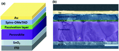 | ||
| Fig. 1 (a) Architecture of a planar perovskite solar cell fabricated with the two-step deposition method. (b) Cross-sectional SEM images of the PMMA device. | ||
In the following sections, we consecutively discuss the degradation induced by a bias voltage, light or heat field. To eliminate the effects of water and oxygen, all devices were encapsulated using glass and epoxy resin. The bias voltage aging process was measured under 1 V under dark conditions and at controlled temperature (25 °C). The entire light aging process was measured using an AM1.5 solar simulator under open circuit conditions and at controlled temperature (25 °C). The heat aging process was measured at controlled temperature (85 °C) under dark conditions. Under the abovementioned aging conditions, the corresponding results of the device performance degradation or kinetic process are discussed in the following sections.
2.2. Voltage-induced rapid degradation
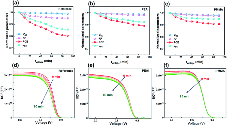
The fast PCE degradation of the encapsulated device in the dark under 1 V is studied. A 1 V bias was applied in the voltage-aging test because the goal of this experiment was to study the effect of 1 V bias on device degradation. However, the 1 V bias can affect the device performance during the measurements. Therefore, no DC bias was applied in the following light-aging and heat-aging tests. In these two experiments, only 10 mV perturbation voltage was applied to the devices. We believe that the perturbation voltage would not lead to significant degradation because its amplitude was negligible compared to the 1 V DC bias and it was applied only for ca. 1 min during each measurement. As shown in Fig. 2, the modified cells have a much better voltage-stability than the reference devices. Using the PEAI or PMMA device, the efficiency can conserve up to 90% of the initial value after 90 min continuous bias voltage application. The reference device has the worst stability, retaining only 80.4% of its original value. The decrease of Jsc is the most significant (85.6%) while the Voc and FF retained 98.8% and 95.1% of their initial values. To investigate the evolution of bulk doping density (N) and the built-in field (Vbi) throughout the voltage-induced rapid degradation, M–S measurement results (capacitance–voltage relationship) measured in the dark (Fig. 2d–f) are analyzed according to the Mott–Schottky relationship,22 | (1) |
According to calculation, after the 90 min voltage-induced rapid degradation, N values of the reference, PEAI and PMMA devices increased from 1.29 × 1016 cm−3 to 1.63 × 10¹⁶ (26.4%↑), from 1.76 × 10¹⁶ to 1.98 × 10¹⁶ (12.5%↑) and from 1.37 × 1016 cm−3 to 1.48 × 1016 cm−3 (8.0%↑), respectively. Namely, N of both modified devices barely changed, implying that the passivation layer can effectively inhibit the voltage-induced doping density increase in the perovskite bulk. This can be attributed to the fact that PEAI and PMMA surface treatments can suppress the formation of charged defects at grain boundaries and surfaces. For example, (1) the π-conjugation structure of the benzene ring of PEAI reduces the neutral iodine related defects; (2) the amine group of PEAI and methyl group of PMMA form a hydrogen bond with the iodide ion and coordinate with the Pb2+ interstitials; and (3) the iodide ions of PEAI fill the iodine vacancies.17,29,39 Simultaneously, the Vbi decreases by 31 mV for the reference devices (from 0.872 to 0.841 V) while it stays almost unchanged for the PMMA and the PEAI devices which agrees with their stable Voc shown in Fig. 2b and c. The apparent inhibition of Vbi and Voc degradation by interface passivation indicates that the Voc degradation of the reference device stems from the interface at the perovskite/charge transport layer, as confirmed by the following discussion based on the EIS results.
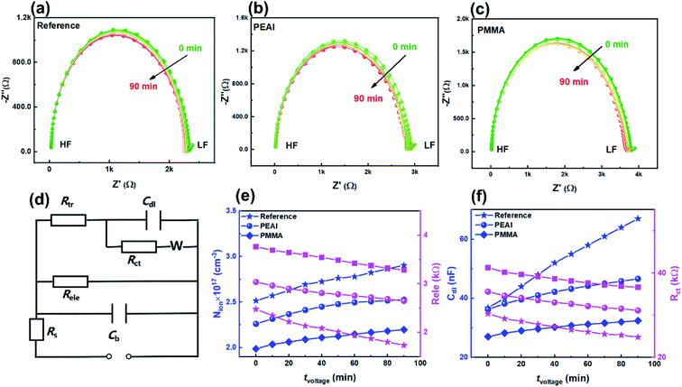
As shown in Fig. 3, the evolution of the EIS results in the Nyquist plots of the reference (a), PEAI (b) and PMMA (c) devices with increasing bias voltage time (tvoltage) under the dark and 1 V conditions is characterized. Each Nyquist plot consists of two obvious features which could be analyzed according to the model and equivalent circuit proposed in previous literature (Fig. 3d).40 In this model, (1) the feature at higher frequency is an arc dominated by free carrier recombination, and (2) the feature at lower frequency is dominated by ion migration which could be modeled with a Warburg element (ZW)23,40
 | (2) |
 | (3) |
According to Fig. 3a–c, during the voltage aging test, the time constants of the resonance peaks stayed almost unchanged (∼10 μs) for all three devices (Fig. S6†), indicating that the free carrier recombination inside the perovskite bulk is unchanged. This agrees with the almost unchanged N and FF.37 Different from the unchanged time constant, Nion shows a moderate increase (Fig. 3e) while Cdl increases the most (Fig. 3f), according to the calculation based on the equivalent circuit fitting and eqn (2) and (3). The significant increase of Cdl indicates the serious accumulation of the mobile ions near the perovskite/charge transport layer interface.40,41 Previous studies showed that the accumulated mobile ions can capture free carriers,42,43 as proved by the significant Rct reduction of the reference device (Fig. 3f). The evolutions of Nion, Cdl and Rct are more obvious in the reference devices than in the passivated devices. In particular, Cdl of the reference device increased by 82.1% which should be responsible for the Jsc loss shown in Fig. 2. In contrast, when the devices are passivated by PEAI or PMMA, Cdl increased by only 28.7% and 20.1%, respectively. According to the above discussion, we conclude that bias voltage mainly affects the interfacial capacitance Cdl (namely, changes the spatial distribution of mobile ions) instead of mobile ion density or static ion dopants. The increase of Cdl originates from ion accumulation at the interface between the perovskite and the charge transport layer,41 which can lead to the perovskite phase segregation, tuning of the band energy diagram, reduction of the free carrier lifetime and shielding of the built-in electric field, thus deteriorating device performance.44–46 The processes involved in the degradation include the halide ion migration, organic cation migration, material decomposition, etc., with timescales of minutes, hours and days, respectively.3,8 Since this work focuses on a reversible and rapid decay process (ca. hours), we believe that the organic cation migration is dominant. Under the bias voltage aging conditions, the direction of the internal electric field is from the ETL to the HTL. Consequently, MA+ ions accumulated at the HTL/perovskite and VMA+ ions at the ETL/perovskite (detailed discussion in ESI Section 2.2).†
Based on previous reports, the Nion increase is related to the decrease of activation energy (Ea).47,48 Non-stoichiometric perovskite can be generated due to phase segregation under the bias voltage conditions.4 Namely, the molar ratio of I to Pb can change from ≥3 (lead-poor or lead-moderate phase) to <3 (lead-rich phase), leading to the lowered Ea of iodine vacancies and interstitial MA+ as confirmed by the first-principles calculation.49 According to the above discussion, we conclude that bias voltage mainly affects the accumulated mobile ions near the interface capacitance Cdl (namely the spatial distribution of mobile ions) which consequently leads to more captured free carriers and lower Jsc. Meanwhile, the mobile ion density increased moderately and the static ion dopant density remains almost unchanged.
2.3. Light-induced rapid degradation
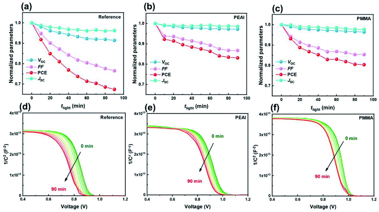
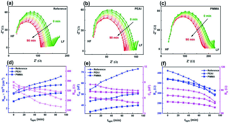
Next, the rapid PCE degradation of the encapsulated devices under AM1.5G continuous illumination is studied. As shown in Fig. 4a–c, after 90 min storage under a light field, the PCEs of the reference, PEAI and PMMA devices decrease to only 67%, 83% and 80% of the initial values, respectively. The PCE loss primarily stems from the FF loss and the Voc loss, although Jsc also dropped a little (3.76%, 1.61% and 2.45% for the reference, PEAI and PMMA devices) like in the voltage aging test. Both the FF loss and the Voc loss can be effectively suppressed by PMMA or PEAI, which agrees with previous research.17,20,23 From the measured M–S results, the initial N of the three devices are calculated to be 1.28 × 10¹⁶, 1.17 × 10¹⁶ and 1.05 × 1016 cm−3 for the reference, PEAI and PMMA devices, respectively. After the 90 min light soaking, the bulk doping densities of all devices only slightly increased to 1.46 × 10¹⁶ (14.0%↑), 1.30 × 10¹⁶ (11.1%↑), and 1.15 × 10¹⁶ (9.5%↑) cm−3 for the reference, PEAI and PMMA devices, respectively, implying no significant change in the concentration of static ions in the perovskite bulk. Aside from N, Vbi of the reference, PEAI and PMMA devices reduced by 83, 47 and 28 mV, respectively, which agrees with their corresponding Voc loss. The apparent inhibition of Vbi and Voc degradation by interface passivation indicates that the light-induced device degradation stems from the interface at the perovskite/carrier transport layer. In the following discussion based on the EIS results, we will show how the light field changes the interface properties and results in Voc reduction.The evolution of the EIS results in the Nyquist plots of the reference (a), PEAI (b) and PMMA (c) devices with increasing light soaking time (tlight) under AM1.5G continuous illumination and open-circuit conditions is characterized. Meanwhile, the corresponding fittings are displayed in Fig. 5d–f. From Fig. 5e, we observe that, with increasing tlight, the Nion for the reference device increases significantly by 52%. These photo-induced mobile ions in the reference device result in the severe FF loss shown in Fig. 4via non-radiative recombination.42 In contrast, the increment ratios in the PMMA and the PEAI devices are only 28% and 34%, respectively. Compared with the reference device, the lower Nion increase in the modified devices proves that the PMMA or PEAI molecules efficiently suppress the conversion of lattice ions on the surface to mobile ions. This is because these passivation molecules tightly bind with the dangling bonds on the lattice surfaces and grain boundaries.17,27,40,50,51 Consequently, the FF reduction of the passivated devices is largely suppressed. Meanwhile, the non-radiative recombination rate of free carriers is studied through analyzing the recombination resistance (Rele).40,52 As shown in Fig. 5d, with increasing tlight, the decrease in Rele for the reference, PEAI and PMMA devices is 30.6%, 19.8% and 12.6%, respectively, indicating that the enhanced recombination probability of the reference is the highest among the three devices. In addition, like in the voltage aging test, the degradation of Cdl and Rct may be the reasons for the slight Jsc drop. The 34% increase in Cdl for the reference device suggests a bad effect on free carrier transport at the interface, which leads to increased interfacial recombination, reflected by the decreased Rct (shown in Fig. 5e). In contrast, when the perovskite was passivated by PEAI or PMMA, the variation of Cdl and Rct became less than 10%. As shown in Fig. 5e and f, we notice that the variation of interface parameters (Cdl, Rct) is greater than the variation of bulk parameters (Cb, Rtr) in both the modified and reference devices. Namely, aside from the interface accumulation observed in the voltage-aging test, the light field also increases Nion, leading to a drop in FF and Voc. Under the light aging conditions, the direction of the internal electric field is from the ETL to the HTL. Consequently, MA+ ions accumulated at the HTL/perovskite and VMA+ ions at the ETL/perovskite (detailed discussion in ESI Section 2.2).† In addition, the PEAI- and PMMA-passivation layer can enhance their stability, leading to slower degradation. Apart from suppression of the formation of charged defects at grain boundaries and surfaces as discussed above, PEAI and PMMA surface treatments can also increase the migration barrier of charged defects. For example, after the conventional 3D perovskite is modified with a 2D perovskite (PEA2PbI4), the migration barrier of ionic defects could increase from 0.680 eV to 0.905 eV, which thereby needs a much higher external field or much longer aging time.53 Based on the above discussion, we consider that PMMA and PEAI modified layers can efficiently suppress ion migration, and consequently slow the performance degradation.
We notice that the PCE drop under the bias voltage aging test process is less significant than under the light aging test. The accelerated degradation under the light aging conditions can be ascribed to (1) phase separation, (2) excess free carriers, and (3) trap charging (neutral iodide).54 Firstly, ion migration is one of the main causes of phase separation, which will result in PCE degradation. In this article, the Nion in the bias voltage (dark) aging test is two orders of magnitude smaller than that in the light aging test which agrees with a previous report, in which the mobile ion density was related to light power.23 Therefore, the phase separation induced degradation phenomenon in the light aging measurement process is more prominent than that under bias voltage aging conditions. Secondly, it has been reported that the excess holes and electrons reduce the Ea for ion migration within PSCs.55 Compared to the bias voltage aging measurement, PSCs in the light aging measurement have a higher concentration of accumulated carriers and consequently lower Ea, resulting in the most severe phase separation.44,45 Thirdly, the accumulated carriers can result in mobile ions becoming trap charging states. For example, the interstitial iodide defect absorbs a free hole to form neutral iodide, which can accelerate the perovskite material's decomposition.54 Based on the above discussion, we conclude that under the bias voltage aging test, the applied electric field mainly drives the preexisting mobile ion accumulation interface and maintains the preexisting mobile ion density. In contrast, under the light aging test, the applied light fields mainly increase the mobile ion density, which subsequently leads to more severe device degradation.
2.4. Heat-induced rapid degradation
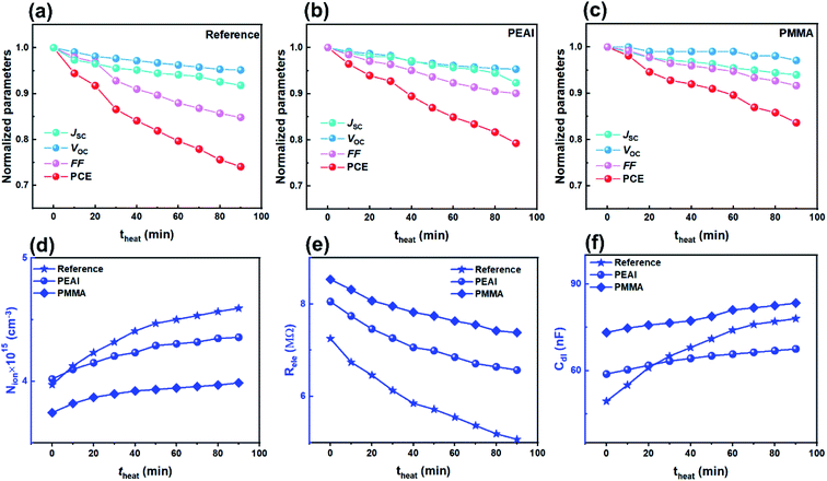
The rapid degradation photovoltaic parameters of the encapsulated devices ((a) for the reference device, (b) for the PEAI device and (c) for the PMMA device) were examined at 85 °C using a thermo plate in the dark. As shown in Fig. 6, after the 90 min heating treatment, the PEAI and PMMA devices retain 79% and 84% of their initial values while the reference perovskite device retains only 74%. The PMMA device has the best stability; the photovoltaic parameters Jsc, Voc and FF retain 92%, 97% and 94% of their initial values.According to the Mott–Schottky relation (Fig. S7†), the calculated N is about 1.49 × 1016 cm−3 (2.59 × 1016 cm−3, 73.8%↑ after heating treatment) for the reference device, 8 × 1015 cm−3 (1.32 × 1016 cm−3, 65.0%↑) for the PEAI device and 7.6 × 1015 cm−3 (1.49 × 1016 cm−3, 96.1%↑) for the PMMA device. Compared to the bias voltage and light aging experiment, after the 90 min heating treatment of the reference device, the relative increases of the static ion dopants in all three devices are significantly higher, regardless of passivation. Therefore, we consider that heat-induced degradation originates from the increased bulk doping densities, instead of interfacial degradation which dominates the bias voltage- or light-induced degradation.
Aside from the increased N, Nion increases with theat, leading to the increase of Cdl (Fig. 6f). Like in voltage and light aging tests, the variation of Nion and Cdl results in a reduced FF and Jsc. Although PEAI and PMMA can alleviate the variation of Nion and Cdl, the performances of the three devices show obvious degradation. Meanwhile, the Rele values of all three devices decrease as shown in Fig. 6e, implying a significantly increased capture probability of the free carriers in the three device types. Therefore, we consider that in the heat aging test, the PCE degradation is largely determined by the decomposition of the perovskite material itself. For example, deep level defects (e.g. metal Pb) could be formed during the decomposition process which could serve as recombination centers, leading to severely reduced FF and PCE.11 In order to confirm the perovskite decomposition, the corresponding XRD experiments were conducted. Compared with light field treatment, the (220) orientation diffraction peaks of all devices are obviously weakened, and almost disappear after 90 min heat field treatment (Fig. S8†), implying more severe perovskite decomposition through volatilization of halide anions or the organic cation,4,9,11 regardless of passivation. In addition, mobile ion migration into the electron/hole transport layer or metal electrode can cause failure of the corresponding functional layer, which will consequently lead to irreversible PCE degradation.56,57 Therefore, during the heat aging process, the decomposition of materials (including the perovskite and functional layer) should be responsible for the degradation of all devices' PCE, which is of distinct difference from the voltage and light aging tests.
In addition, the reason for the increase of Nion under heating can also be ascribed to perovskite decomposition. It is well known that perovskite thermal decomposition can generate more voids or pinholes confirmed by scanning electron microscopy,4 which results in a higher surface/volume ratio than in the fresh perovskite. Experiment and theory have proved that perovskites with a higher surface/volume ratio have a lower Ea than those with a smaller surface/volume ratio.47,58 Consequently, under the heat aging process, the evolution of micro-morphology is one of the reasons leading to the change of Ea, which leads to increased Nion.
3. Conclusion
By comparing the three aging tests, we find that the bias voltage field is the least effective in facilitating device degradation while the light field and heat field are similarly effective. The light-induced and heat-induced degradation processes are both dominant with reduced FF while the voltage-induced degradation is dominant with reduced Jsc. The dominant mechanisms of the degradation under voltage, light and heat fields are different (Fig. 7). (a) The voltage field only results in accumulation of preexisting mobile ions near the interface; (b) the light field results in photo-induced mobile ions, leading to more severe mobile ion accumulation than in the voltage aging test; (c) the heat field results in material decomposition (including that of perovskite and functional layers). Through the comparison of the three types of device, we find that the polymer organic layer (PMMA) and low dimensional perovskite (PEAI) can efficiently suppress ion migration, especially the voltage and light-induced migration, which consequently improve the stability. However, the modified layer can't effectively alleviate the heat-induced degradation, which stems from perovskite decomposition. Therefore, to improve its thermal stability, it is not only necessary to inhibit ion migration from the perspective of interface engineering, but also to enhance the Ea of ion migration of the material itself through component engineering.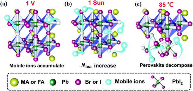 | ||
| Fig. 7 Schematic of the effect of the external field on mobile ions under light (a), bias voltage (b) and heat conditions (c). | ||
Conflicts of interest
There are no conflicts to declare.Acknowledgements
This work was financially supported by the General Program of Science and Technology Development Project of Beijing Municipal Education Commission (No. KM202010005005), National Natural Science Foundation of China (No. 62034001, 61922005, 61974008, 5207101067), Beijing Natural Science Foundation (BNSF) under Grant No. JQ20027, Beijing Nova Program of Science and Technology under Grant No. Z191100001119116, and the International Research Cooperation Seed Fund of Beijing University of Technology (No. 2021B07).References
- L. Meng, J. You and Y. Yang, Nat. Commun., 2018, 9, 1–4 CrossRef CAS PubMed.
- B. W. Park and S. I. Seok, Adv. Mater., 2019, 31, 1805337 CrossRef PubMed.
- K. Domanski, B. Roose, T. Matsui, M. Saliba, S.-H. Turren-Cruz, J.-P. Correa-Baena, C. R. Carmona, G. Richardson, J. M. Foster, F. De Angelis, J. M. Ball, A. Petrozza, N. Mine, M. K. Nazeeruddin, W. Tress, M. Grätzel, U. Steiner, A. Hagfeldt and A. Abate, Energy Environ. Sci., 2017, 10, 604–613 RSC.
- Y.-H. Lin, N. Sakai, P. Da, J. Wu, H. C. Sansom, A. J. Ramadan, S. Mahesh, J. Liu and R. D. Oliver, Science, 2020, 369, 96–102 CrossRef CAS PubMed.
- J.-W. Lee, S.-G. Kim, J.-M. Yang, Y. Yang and N.-G. Park, APL Mater., 2019, 7, 041111 CrossRef.
- R. Wang, M. Mujahid, Y. Duan, Z.-K. Wang, J. Xue and Y. Yang, Adv. Funct. Mater., 2019, 29, 1808843 CrossRef CAS.
- Y. Zhou and Y. Zhao, Energy Environ. Sci., 2019, 12, 1495–1511 RSC.
- H. Wang, A. Guerrero, A. Bou, A. M. Al-Mayouf and J. Bisquert, Energy Environ. Sci., 2019, 12, 2054–2079 RSC.
- D. B. Khadka, Y. Shirai, M. Yanagida and K. Miyano, J. Mater. Chem. C, 2018, 6, 162–170 RSC.
- S. N. Raja, Y. Bekenstein, M. A. Koc, S. Fischer, D. Zhang, L. Lin, R. O. Ritchie, P. Yang and A. P. Alivisatos, ACS Appl. Mater. Interfaces, 2016, 8, 35523–35533 CrossRef CAS PubMed.
- N. Li, Y. Luo, Z. Chen, X. Niu, X. Zhang, J. Lu, R. Kumar, J. Jiang, H. Liu, X. Guo, B. Lai, G. Brocks, Q. Chen, S. Tao, D. P. Fenning and H. Zhou, Joule, 2020, 4, 1743–1758 CrossRef CAS.
- S. T. Birkhold, J. T. Precht, R. Giridharagopal, G. E. Eperon, L. Schmidt-Mende and D. S. Ginger, J. Phys. Chem. C, 2018, 122, 12633–12639 CrossRef CAS.
- G. Divitini, S. Cacovich, F. Matteocci, L. Cinà, A. Di Carlo and C. Ducati, Nat. Energy, 2016, 1, 1–6 Search PubMed.
- W. Chen, W. Li, Z. Gan, Y.-B. Cheng, B. Jia and X. Wen, Chem. Mater., 2019, 31, 9049–9056 CrossRef CAS.
- G. Xia, B. Huang, Y. Zhang, X. Zhao, C. Wang, C. Jia, J. Zhao, W. Chen and J. Li, Adv. Mater., 2019, 31, 1902870 CrossRef PubMed.
- W. Fu, H. Liu, X. Shi, L. Zuo, X. Li and A. K. Y. Jen, Adv. Funct. Mater., 2019, 29, 1900221 CrossRef.
- Q. Jiang, Y. Zhao, X. Zhang, X. Yang, Y. Chen, Z. Chu, Q. Ye, X. Li, Z. Yin and J. You, Nat. Photonics, 2019, 13, 460–466 CrossRef CAS.
- D. S. Lee, J. S. Yun, J. Kim, A. M. Soufiani, S. Chen, Y. Cho, X. Deng, J. Seidel, S. Lim, S. Huang and A. W. Y. Ho-Baillie, ACS Energy Lett., 2018, 3, 647–654 CrossRef CAS.
- Y. Liu, S. Akin, L. Pan, R. A. Uchida, N. Arora, J. V. H. Milić, A. Hinderhofer, F. Schreiber, A. R. Z. Uhl, S. M. Zakeeruddin, A. D. Hagfeldt, M. Ibrahim and M. Grätze, Sci. Adv., 2019, 5, eaaw2543 CrossRef CAS PubMed.
- S. Kundu and T. L. Kelly, Mater. Chem. Front., 2018, 2, 81–89 RSC.
- A. A. Maxim, S. N. Sadyk, D. Aidarkhanov, C. Surya, A. Ng, Y. H. Hwang, T. S. Atabaev and A. N. Jumabekov, Nanomaterials, 2020, 10, 291 CrossRef CAS PubMed.
- M. Fischer, K. Tvingstedt, A. Baumann and V. Dyakonov, ACS Appl. Energy Mater., 2018, 1, 5129–5134 CAS.
- X. Chen, Y. Shirai, M. Yanagida and K. Miyano, J. Phys. Chem. C, 2019, 123, 3968–3978 CrossRef CAS.
- Y. Feng, J. Bian, S. Wang, C. Zhang, M. Wang and Y. Shi, J. Mater. Chem. C, 2019, 7, 8294–8302 RSC.
- I. Zarazua, G. Han, P. P. Boix, S. Mhaisalkar, F. Fabregat-Santiago, I. Mora-Sero, J. Bisquert and G. Garcia-Belmonte, J. Phys. Chem. Lett., 2016, 7, 5105–5113 CrossRef CAS PubMed.
- N. A. Nadege Ouedraogo, M. Yang, C. He, Y. Chen, X. Zhang, H. Yan, C. B. Han and Y. Zhang, Sustainable Energy Fuels, 2020, 4, 4257–4263 RSC.
- Y. Chen, Q. Meng, Y. Xiao, X. Zhang, J. Sun, C. B. Han, H. Gao, Y. Zhang, Y. Lu and H. Yan, ACS Appl. Mater. Interfaces, 2019, 11, 44101–44108 CrossRef CAS PubMed.
- E. Aydin, M. De Bastiani and S. De Wolf, Adv. Mater., 2019, 31(25), e1900428 CrossRef PubMed.
- B. Chen, P. N. Rudd, S. Yang, Y. Yuan and J. Huang, Chem. Soc. Rev., 2019, 48, 3842–3867 RSC.
- E. Bi, W. Tang, H. Chen, Y. Wang, J. Barbaud, T. Wu, W. Kong, P. Tu, H. Zhu, X. Zeng, J. He, S.-I. Kan, X. Yang, M. Grätzel and L. Han, Joule, 2019, 2748–2760 CrossRef CAS.
- O. Hentz, A. Singh, Z. Zhao and S. Gradečak, Small Methods, 2019, 3, 1900110 CrossRef.
- W. Jiang, J. Ying, W. Zhou, K. Shen, X. Liu, X. Gao, F. Guo, Y. Gao and T. Yang, Chem. Phys. Lett., 2016, 658, 71–75 CrossRef CAS.
- W. Li, W. Zhang, S. Van Reenen, R. J. Sutton, J. Fan, A. A. Haghighirad, M. B. Johnston, L. Wang and H. J. Snaith, Energy Environ. Sci., 2016, 9, 490–498 RSC.
- Y. Lin, Y. Bai, Y. Fang, Z. Chen, S. Yang, X. Zheng, S. Tang, Y. Liu, J. Zhao and J. Huang, J. Phys. Chem. Lett., 2018, 9, 654–658 CrossRef CAS PubMed.
- Y. Lin, Y. Bai, Y. Fang, Q. Wang, Y. Deng and J. Huang, ACS Energy Lett., 2017, 2, 1571–1572 CrossRef CAS.
- S. G. Motti, D. Meggiolaro, S. Martani, R. Sorrentino, A. J. Barker, F. De Angelis and A. Petrozza, Adv. Mater., 2019, 31, 1901183 CrossRef CAS PubMed.
- J. Wu, J. Shi, Y. Li, H. Li, H. Wu, Y. Luo, D. Li and Q. Meng, Adv. Energy Mater., 2019, 9, 1901352 CrossRef CAS.
- U. T. Ravishankar Sandheep and K. Thomas, Science, 2021, 371, 6484 Search PubMed.
- L. Fu, H. Li, L. Wang, R. Yin, B. Li and L. Yin, Energy Environ. Sci., 2020, 13, 4017–4056 RSC.
- E. C. Smith, C. L. C. Ellis, H. Javaid, L. A. Renna, Y. Liu, T. P. Russell, M. Bag and D. Venkataraman, J. Phys. Chem. C, 2018, 122, 13986–13994 CrossRef CAS.
- C. Aranda, J. Bisquert and A. Guerrero, J. Chem. Phys., 2019, 151, 124201 CrossRef PubMed.
- H. Chen, X. Wen, R. S. Sheng, S. Huang, X. Deng, M. A. Green and A. Ho-Baillie, ACS Appl. Mater. Interfaces, 2016, 8, 5351–5357 CrossRef PubMed.
- G. H. Isaac Zarazua, P. P. Boix, S. Mhaisalkar, F. Fabregat-Santiago, I. Mora-Seró, J. Bisquert and G. Garcia-Belmonte, J. Phys. Chem. Lett., 2016, 7, 5105–5113 CrossRef PubMed.
- T.-Y. Zhu and D.-J. Shu, J. Phys. Chem. C, 2019, 123, 5312–5320 CrossRef CAS.
- L. Bertoluzzi, C. C. Boyd, N. Rolston, J. Xu, R. Prasanna, B. C. O'regan and M. D. Mcgehee, Joule, 2019, 4, 109–127 CrossRef.
- D. Moia, I. Gelmetti, P. Calado, W. Fisher, M. Stringer, O. Game, Y. Hu, P. Docampo, D. Lidzey, E. Palomares, J. Nelson and P. R. F. Barnes, Energy Environ. Sci., 2019, 12, 1296–1308 RSC.
- D. Meggiolaro, E. Mosconi and F. D. Angelis, ACS Energy Lett., 2019, 4, 779–785 CrossRef CAS.
- J. M. Azpiroz, E. Mosconi, J. Bisquert and F. D. Angelis, Energy Environ. Sci., 2015, 8, 2118–2127 RSC.
- W. Yin, T. Shi and Y. Yan, Appl. Phys. Lett., 2014, 104, 063903 CrossRef.
- J. Yang, C. Liu, C. Cai, X. Hu, Z. Huang, X. Duan, X. Meng, Z. Yuan, L. Tan and Y. Chen, Adv. Energy Mater., 2019, 1970064 CrossRef.
- E. C. Smith, C. L. C. Ellis, H. Javaid, B. G. Arden and D. Venkataraman, Phys. Chem. Chem. Phys., 2019, 21, 20720–20726 RSC.
- M. N. F. Hoque, N. Islam, Z. Li, G. Ren, K. Zhu and Z. Fan, ChemSusChem, 2016, 9, 2692–2698 CrossRef CAS PubMed.
- C. Chen, Z. Song, C. Xiao, R. A. Awni, C. Yao, N. Shrestha, C. Li, S. S. Bista, Y. Zhang, L. Chen, R. J. Ellingson, C.-S. Jiang, M. Al-Jassim, G. Fang and Y. Yan, ACS Energy Lett., 2020, 5, 2560–2568 CrossRef CAS.
- V. K. Mark, K. M. Anoop, A. K. Eugene and V.-F. Iris, Energy Environ. Sci., 2019, 12, 550–558 RSC.
- Y. Lin, B. Chen, Y. Fang, J. Zhao, C. Bao, Z. Yu, Y. Deng, P. N. Rudd, Y. Yan, Y. Yuan and J. Huang, Nat. Commun., 2018, 9, 1–9 CrossRef PubMed.
- M.-W. An, Z. Xing, B.-S. Wu, F.-F. Xie, S.-Y. Zheng, L.-L. Deng, X. Wang, B.-W. Chen, D.-Q. Yun, S.-Y. Xie, R.-B. Huang and L.-S. Zheng, Rare Met., 2020, 40, 1691–1697 CrossRef.
- K. Domanski, J.-P. Correa-Baena, N. Mine, M. K. Nazeeruddin, A. Abate, M. Saliba, W. Tress, A. Hagfeldt and M. Grätzel, ACS Nano, 2016, 10, 6306–6314 CrossRef CAS PubMed.
- J. Xing, Q. Wang, Q. Dong, Y. Yuan, Y. Fang and J. Huang, Phys. Chem. Chem. Phys., 2016, 18, 30484–30490 RSC.
Footnote |
| † Electronic supplementary information (ESI) available. See DOI: 10.1039/d1na00495f |
| This journal is © The Royal Society of Chemistry 2021 |

