
 Open Access Article
 This Open Access Article is licensed under a Creative Commons Attribution-Non Commercial 3.0 Unported Licence
Dynamic photonic perovskite light-emitting diodes with post-treatment-enhanced crystallization as writable and wipeable inscribers†
Sheng
Bi
 a,
Wei
Zhao
a,
Yeqing
Sun
a,
Chengming
Jiang
*a,
Yun
Liu
b,
Zhengran
He
c,
Qikun
Li
a and
Jinhui
Song
*a
a,
Wei
Zhao
a,
Yeqing
Sun
a,
Chengming
Jiang
*a,
Yun
Liu
b,
Zhengran
He
c,
Qikun
Li
a and
Jinhui
Song
*a
aKey Laboratory for Precision and Non-traditional Machining Technology of the Ministry of Education, School of Mechanical Engineering, Dalian University of Technology, Dalian 116024, China. E-mail: jiangcm@dlut.edu.cn; jhsong@dlut.edu.cn
bDepartment of Mechanical Engineering, University of Maryland, College Park, MA 20742, USA
cCenter for Materials for Information Technology, The University of Alabama, Tuscaloosa, AL 35487, USA
First published on 15th September 2021
Abstract
Controllable photonic patterns have attracted great attention for various applications in displays, smart sensors, and communications. Conventional patterned light-emitting-diode (LED) systems require complicated design, complex procedure, and advanced equipment. Moreover, permanent properties of the fabricated patterns on LED restrict it from various important applications. Herein, we present an innovative writable and wipeable perovskite light-emitting-diode (WWPeLED) device, which tactfully utilizes the large variation of turn-on voltage originating from the external quantum efficiency (EQE) difference under controllable thermal treatment. The turn-on voltages with/without thermal-treatment devices exhibit a large gap of over 5 V, and the thermal-treatment electroluminescence intensity is more than 10 times higher than that of non-thermal-treatment devices. The new phenomena open up an effective way of controlling illumination with desired pattern designs. Additionally, the distinct handwriting fonts and habits as well as printing patterns with illumination WWPeLED are also realized. Furthermore, these written and printed features can be totally wiped out with an 11 V cleaning voltage, turning the devices as a regular fully bright PeLED. The stability and repeatability tests prove the robustness of WWPeLED in both mechanical and electroluminescence performance after a long period of operations. The innovative WWPeLED devices may find prospective applications in various optoelectronic devices and flexible integrated systems.
1. Introduction
Light-emitting diode patterning1–3 is becoming a crucial and express technology for multifarious optical applications in independent and various graphics displays,4–6 sensors7–9 and optical devices10–12 attributed to the excellent reaction to external conditions, especially for coding that requires convenient and rapid patterning as well as effortless pattern removal processes, in which graph designing has been widely applied in anticounterfeiting13,14 and secure communication.15,16 The two main patterning methods applied nowadays for fabricating light-emitting diode (LED) displays are thermal evaporation through shadow masks and ink-jet printing,17,18 which are comparably too inefficient for industries,19,20 and incompatible with a large amount of organic materials.21 Photolithography, which is the widely used patterning method in the industry for inorganic light-emitting diodes, is incompatible for organic light-emitting diodes (OLEDs) due to the vulnerability of the organic materials to chemical reactions involved in the process.22–25 However, until now, hoisting the capacity of fantastic performance of patterned OLEDs is required with excellent device designs, outstanding experimental equipment, and rich experimental experience. The OLED patterning application is still limited due to the lack of an economical and sufficient approach for patterning organic materials.However, a group of inorganic CsPbX3 (X = Cl, Br, and I) perovskites have been extensively developed for their potential optoelectronic applications due to high luminance, high photoluminescence quantum yields (>90%), solution processability, pure emission (full width at half-maxima (FWHM < 20 nm)), and exceptional thermal stability, which make CsPbX3 an excellent choice for use as the emission material in perovskite-based LEDs (PeLEDs).26–31
Herein, we introduce an innovative writable and wipeable perovskite LED (WWPeLED) device, which is enabled by external quantum efficiency (EQE) control via thermal processing. By temperature treatment on the desired region of the perovskite films of the WWPeLED, the molecular crystal configuration as well as the bonding mode and strength rearrange, leading to different turn-on voltages and EQE between the thermally treated part and the untreated area. The patterned features are able to be fully wiped-out by applying a higher operating voltage, which increases the temperature on the entire perovskite films, improving the crystallinity of the entire area, as well as decreasing the turn-on voltage to form a regular PeLED. Stability and repeatability prove the robustness of the WWPeLED devices in both mechanical and electroluminescence (EL) performance after a long period of operations, making them reliable for practical applications. The WWPeLED device presents huge potential to enlighten and promote the development of sufficient identification characters for anti-counterfeiting, sensing and optoelectronic applications.
2. Results and discussion
The schematic structure of the designed WWPeLED is shown in Fig. 1a, which employs CsPbBr3 as an emission material in the middle, sandwiched by LiF and poly(3,4-ethylenedioxythiophene)polystyrene sulfonate (PEDOT:PSS), at the top and bottom as electron and hole transport layers, respectively. Indium tin oxide (ITO) as an anode is sputtered onto a poly(ethylene terephthalate) (PET) film, serving as the flexible and conductive substrate, followed by PEDOT:PSS spun-coat as a hole transfer layer. An Al film is at last thermally deposited on the very top of the device as a cathode. Then, a heating pen is applied to the desired area on the WWPeLED surface to write/print a designed pattern. The heat-treated area with patterns can be illuminated with a low applied voltage, while other areas still remain in “off-status”, as illustrated in Fig. 1b and c. To effectively realize this unique phenomenon, the device is first merged in a liquid nitrogen environment after the fabrication process of CsPbBr3 deposition. This extremely low temperature reduces the bonding force of CsPbBr3 molecules, thus the molecules of CsPbBr3 are anisotropically distributed,32,38,39 leading to an inferior crystallization state with little macroscopic crystal alignment formed. Upon thermal treatment on the WWPeLED, CsPbBr3 molecules rearrange to become high-quality aligned-up crystal units.33–35 To systematically study this crystalline phenomenon in WWPeLED, the electrical performance of the devices is carefully investigated by applying different treatment temperatures. The current density versus applied voltage (J–V) curves are plotted in Fig. 1d, presenting a strong response increment to the voltage with the increase in treatment temperature. Moreover, within a certain extent of treatment temperature (0–300 °C), a lower turn-on voltage is required for devices treated at higher temperatures to reach the same EL intensity, which results from the higher crystallinity of the emission layer, as shown in the inset of Fig. 2a. The process time is less than 2 seconds, which do not do any harm to the substrate as well as to other functional layers. However, the luminance of the WWPeLED also highly depends on the treatment temperature, as plotted in Fig. 1e. A turn-on voltage difference up to 5 V is observed between the fabricated device treated at 300 °C and 25 °C. With the same loading voltage, the WWPeLED thermally treated at 25 °C cannot be turned on, while only dim light illumination is observed from the device treated at 100 °C. A bright and sharp light is noticed from the device under 300 °C treatment, indicating that a relatively large difference of turn-on voltage is required for the devices from various treatment temperatures.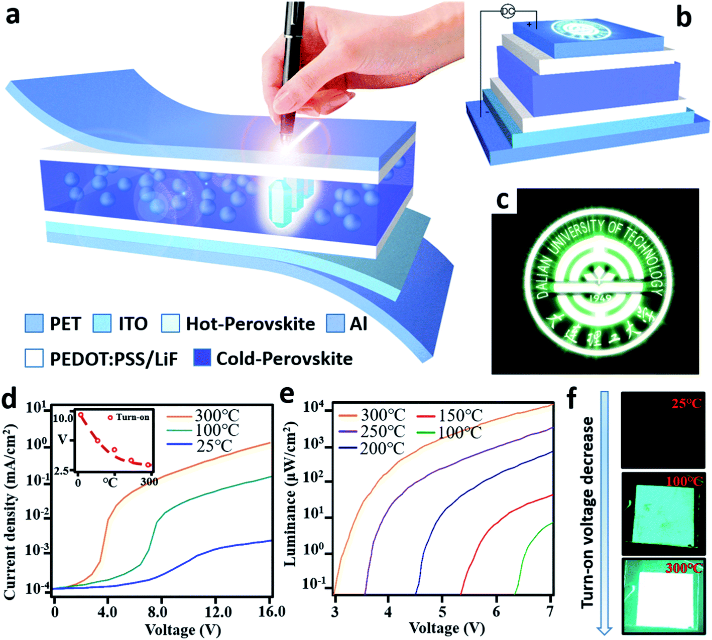 | ||
| Fig. 1 Schematic configuration of the WWPeLED device and electrical and illumination characteristics of CsPbBr3 films under different treatment temperatures. (a) Schematic of WWPeLED devices made of an ITO-coated PET film as a flexible substrate, PEDOT:PSS as a hole transport layer, low-temperature crystallization CsPbBr3 as an emitter, and LiF/Al as a cathode. The structure of amorphous form CsPbBr3 randomly distributes in the emitter layer under the cold-treated crystallized, and the emitter structure trends to crystalize where the surface is heated by a thermal pen. (b) Electroluminescent pattern with a connecting circuit for the WWPeLED with the heated area on the top of the surface. (c) Illustration of the WWPeLED with the illuminated pre-design pattern after heat treatment. (d) Plot of current density versus voltage for the WWPeLED under different treatment temperatures. The higher the post processing temperature, the stronger the current response with the applied voltage. The inset is the corresponding turn-on voltage versus temperature. (e) Luminance variation with the working voltage of the WWPeLED treated at different post-processing temperatures. (f) Photo of the WWPeLED with the same voltage at different post-processing temperatures. With the same voltage of 6 V, the device at 25 °C is dark, while the one at 300 °C becomes noticeably bright. | ||
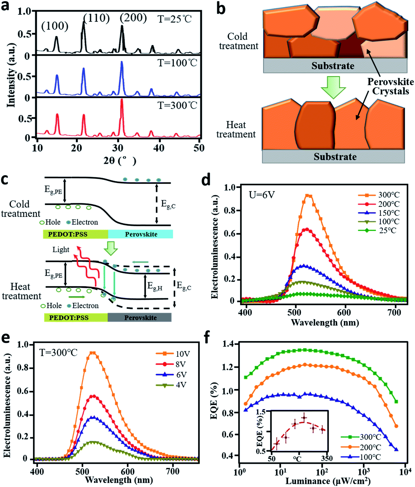 | ||
| Fig. 2 Crystallization principle of pristine and annealed CsPbBr3 in the WWPeLED, and the electrical and illumination characterization of the WWPeLED under different treatment conditions. (a) XRD spectrum of crystallization CsPbBr3 films at different treatment temperatures. Highly crystalline perovskites along the (100), (110) and (200) orientations prove the formation of highly crystallized crystals. The magnitude and height of the diffraction peaks change while maintaining the same peak position. (b) Schematic of the crystal orientation change in the emitting layer. The CsPbBr3 irregularly concretes under cold circumstances (25 °C) and can directly transfer to well-aligned crystals after heat treatment (>100 °C). (c) Energy band diagrams between PEDOT:PSS and CsPbBr3 for the different temperature crystalline states. With 25 °C treatment, the anisotropic structure leads to a wide bandgap, leading to a larger distance for electrons and holes to recombine and generate light. With the >100 °C annealing temperature on the emitting layer, the crystallinity of the film decreases the width of bandgap, providing a higher charge recombination efficiency. (d) Emission spectrum of the WWPeLED at different treatment temperatures with the bias of 6 V. (e) EL spectrum of WWPeLED alters the applied voltage from 4 V to 10 V at 300 °C postprocessing temperature. (f) EQE variation of the devices under three different postprocessing temperatures (100 °C, 200 °C, and 300 °C). The maximum EQE value can arrive when the luminance is around 50 μW cm−2. The inset shows in detail the variation in EQE with different postprocessing temperatures. | ||
In order to explore the crystallization principle of the CsPbBr3 emission before and after heat treatment, a detailed analysis on the formation of the molecule crystal was carried out. It is clearly shown in the X-ray diffraction (XRD) spectra of CsPbBr3 in Fig. 2a under different treatment temperatures that a highly crystalline perovskite is grown along the (100), (110) and (200) orientations, proving the formation of highly crystallized crystals. The magnitude and height of the diffraction peaks change while maintaining the same peak position, indicating that the degree of crystallinity and the crystal orientation vary with the treatment temperature but not cubic phase. For a better understanding, a theoretical illustration is drawn in Fig. 2b. Before annealing the films, the crystals are not well crystallized into big ones, leading to comparably random orientation configuration. When the CsPbBr3 layer is treated with heat, the crystals trend to aggregate to become a whole and parallel arrangement, which is proved in the XRD spectra where purer crystal orientation is observed in the layer treated at 300 °C.
To reveal the electrical theories behind this phenomenon, the band diagrams between PEDOT:PSS and CsPbBr3 were carried out, as shown in Fig. 2c, where the bandgap between the highest occupied molecular orbits (HOMO) and the lowest unoccupied molecular orbits (LUMO) of CsPbBr3 alters with/without the heat-treatment. When the molecules of CsPbBr3 are disorientated with low crystallinity under cold circumstance, the bandgap extends so that the holes from the anode and electrons from the cathode desire to travel a larger span to recombine and generate light, leading to low EQE and high turn-on voltage.36,37 When the device goes through heat treatment, the molecules of CsPbBr3 are well aligned and highly crystallized, and the bandgap between HOMO and LUMO becomes narrower, so that the charges travel a shorter distance to recombine and generate photons. Thus, it dramatically improves the EQE as well as decreases the turn-on voltage. Then, the luminescence characteristics of WWPeLED under different treatment temperatures are also carefully studied. At the same bias, the devices treated at a higher temperature tend to possess higher luminance. Fig. 2d plots the typical luminescence spectrum of the WWPeLED under different treatment temperatures with the voltage fixed at 6 V with the emission peak of 520 nm. The corresponding influence of the voltage with a fixed treatment temperature of 300 °C is also meticulously researched, as plotted in Fig. 2e. The asymmetric emission is associated with the nonhomogeneous distribution of cations in CsPbBr3 single crystals. The unraveling of a correlation between the composition, growth, and spectroscopic properties of perovskite crystals in the nanoregime arguably dictates the overall performance of the device. The brightness increment rate decreases with the temperature and voltage, which is mainly due to the EQE variation in the device, as shown in Fig. 2f, where EQEs of the three devices are presented as a function of the luminance, and the corresponding detailed device efficiency characteristics in dependence of the treatment temperature are summarized as the inset in Fig. 2f, in which the maximum EQE of 0.9%, 1.2% and 1.35% is observed at around 50 μW cm−2 for the three devices at 100 °C, 200 °C and 300 °C thermal treatments, respectively. Comparing the highest EQE among devices, 300 °C treatment temperature provides the best illuminated performance.
The novel and special characteristics of the WWPeLED are a desirable implement for recording handwriting features. The pre-fabricated WWPeLED without the annealing process is first treated by cold temperature for heat-writing. A heat pen with 300 °C swipes letters over the WWPeLED, as shown in Fig. 3a. A handwritten letter “U” shows up and the picture is taken in Fig. 3b with the supplying voltage to the WWPeLED. The analysis of the EL intensity distribution of the bright “U” is presented in Fig. 3c. Uniform light intensity is found in each part of the letter with a maximum intensity of 0.08 mW cm−2. The line profiles of the two regions of the illuminated letter marked by red and blue dash lines, shown in Fig. 3d, obviously prove even intensity distribution, suggesting the stability of the local heating technology from handwriting. Fig. 3e clearly records the handwriting process using a high-speed camera at a time interval of 2 s to display several consecutive images, where a distinct movement track of the heat pen is legibly recorded. Fig. 3f demonstrates the handwriting fonts and features from signees using WWPeLED. The brightness and the width of the letters are dependent on the writing distance and the moving speed. The short writing distance and the long staying time on the surface of the device result in brighter and wider marks. The analysis of the intensity distribution at the bottom demonstrates the uniform brightness and clearly reveals the difference in relative intensities among the four different signees. Therefore, the WWPeLED is a comparably precise device for recording the handwriting fonts as well as the features of the signees.
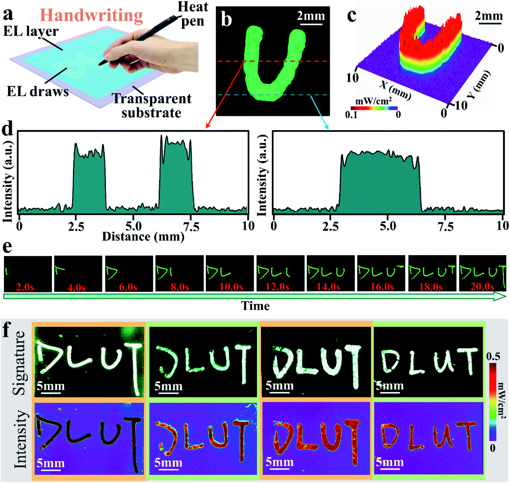 | ||
| Fig. 3 Visualization of dynamic handwriting on the WWPeLED. (a) Schematic of the handwriting recording demonstration. Under the working bias, the “letter” can be directly appeared on the WWPeLED with a heat pen. (b) Photo of electroluminescent handwritten letter “U”. The scale bar is 2 mm. (c) Intensity distribution of the luminescent letter “U”. The intensity evenly distributed at each part of the letter. The maximum power of the luminescence is 0.08 mW cm−2. (d) The corresponding 2D distribution of the relative EL intensity derived by extracting the photo from (b). Both the middle and the bottom data of the letter show similar emission intensities. (e) Consecutive frames extracted from the dynamically capture video of the handwriting process based on a 2 s time interval. (f) Photos of the handwriting fonts recording four signees by WWPeLED devices. The brightness as well as the width of the letters is dependent on the distance of pen-surface and the moving speed from the signees. The intensity distribution diagram clearly demonstrates the handwriting difference with different personalizations. | ||
WWPeLED can also present 3D images by a thermal printing pattern. Fig. 4a shows the schematic of printing patterns onto WWPeLED, in which the pattern is pre-fabricated on a stamp with a 3-dimensional concave and convex mold followed by 300 °C treatment by four springs support. When it is used to print patterns, the cold-treated WWPeLED is placed beneath the stamp and the stamp is pressed down onto the device for seconds. The emblem of “Dalian University of Technology” was first printed and presented in Fig. 4b, where detailed information was entirely “copied” onto the illuminative part of the WWPeLED. Fig. 4c shows the intensity of the emblem in a 2D and 3D point of view, where there is a strong contrast between light and darkness, indicating a high quality of the printing method. As shown in Fig. 4d, more complex and designed patterns were also produced by the thermal printing method onto the WWPeLED, with “Watermelon”, “maple leaf” and “lily flower” as three of the examples with clear detailed patterns and stripes in various shapes with different dimensions. Moreover, after increasing the working voltage for the three devices, a 3-dimensional stereo sense emerges in both “watermelon” and “lily flower”. The brighter illuminant at the edge highlights the spherical three-dimensional structure of the “watermelon”, which exactly matches the shapes of the molds, where the background is slightly higher than the middle of the pattern, so that the surrounding area touches the WWPeLED firmly, while a tiny space at the middle part is remained between the mold and device, leading to a stronger light at the edge than in the middle. The same design was carried out and the same phenomenon was observed in petals of the “lily flower”. It is proved that the technique is time-saving and low-cost for 3-dimensional pattern PeLED technique.
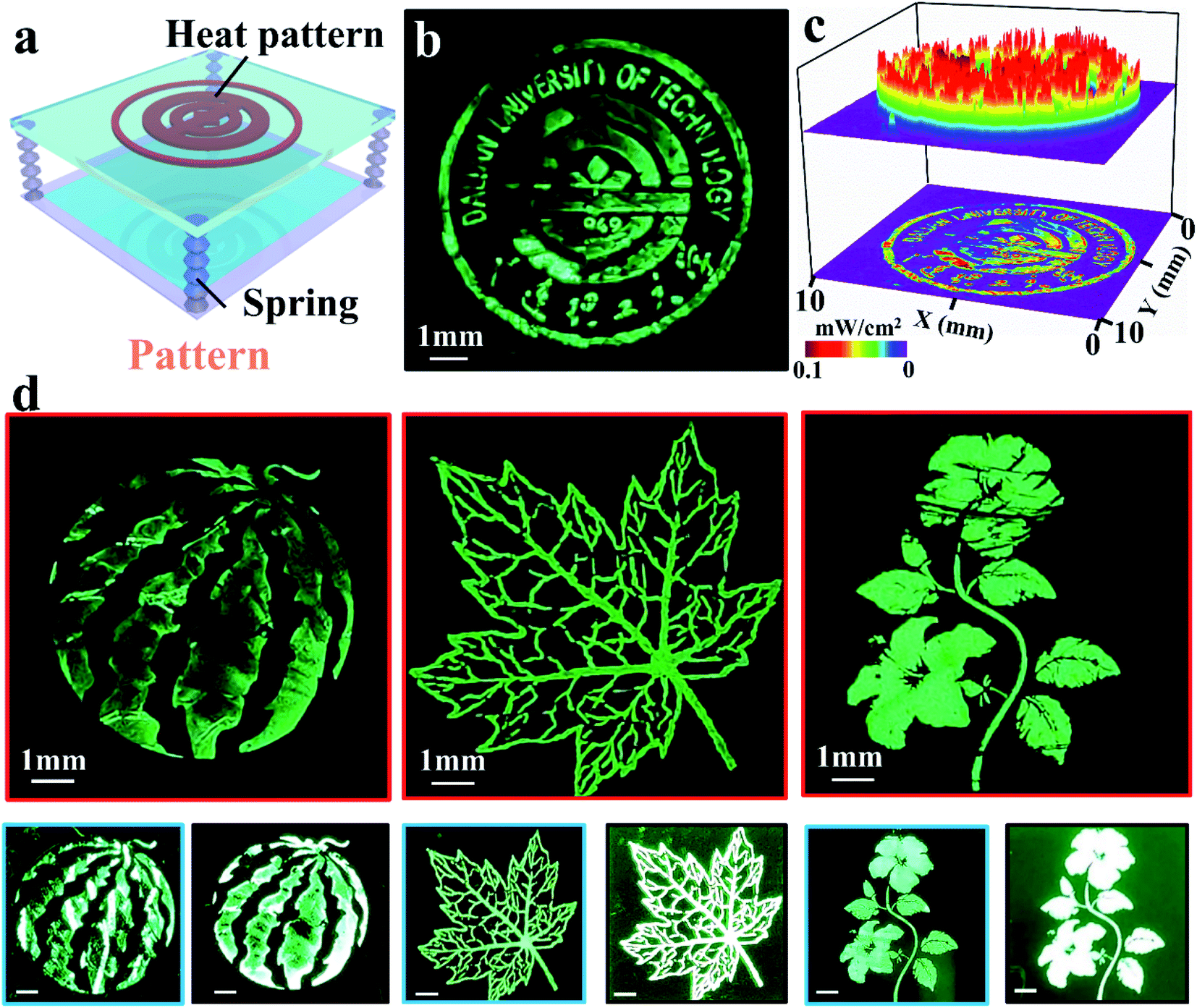 | ||
| Fig. 4 Printable characteristics and performance of the WWPeLED. (a) Schematic of the 2D planar print on the device. The spring is applied to assist controlling the print hardness and time. (b) Printed emblem of “Dalian University of Technology”. (c) Both 3D and 2D intensity distribution analyses of the emblem. The maximum brightness intensity is approximately 0.08 mW cm−2. (d) Printed “watermelon”, “maple leaf” and “lily flower” PeLED with power supply for illumination. By increasing the power for the “watermelon”, 3D visual perception emerges, which exactly follows the design of the printing mold. Unambiguous, complex and narrow “maple” lines are clearly seen. The “lily flower” also shows a stereoscopic sense on the petal. | ||
Besides the capability of handwriting and printing on WWPeLED devices, the patterns or letters can be totally wiped out to act as a regular PeLED, whose procedure is shown in Fig. 5a. In a pattern making process, the applied voltage on a written or printed device is controlled below 10 V, where the pattern or letter lights up with the surrounding area to be dark, so that the pattern or letter can be clearly observed. Continue to increase the applied voltage to ∼11 V, and the dark region on the substrate starts to “burn” and gradually light-up to the entire substrate as a whole luminous regular planar PeLED. This is due to the heat generation from the electric radiates applied on the devices and the generated heat facilitates the crystallization of the film (seen from XRD curves in Fig. 2a), leading to a decrease in turn-on voltage until it reaches the same level with the previous lit-up letter or pattern areas, and the luminant intensity becomes consistent throughout the sample. Thus, patterns or letters appear to be wiped out from the substrate, as the luminance of the patterns or letters is the same with the surrounding area. A systematic study on the influence of the wiping voltage is carried out and plotted in Fig. 5b. By applying a high voltage of 11 V, the electrical-generated heat is more than that achieved at low voltages, resulting in a decreased turn-on voltage with faster lit-up speed and brighter emitting intensity. Fig. 5c shows the PeLED performance after patterns or letters are wiped out, presenting the same turn-on voltage, response time and the saturation level, independent of the wiping voltages. The EQE variation data in the inset further prove that the WWPeLED exhibits constant performance after wiping, which does not rely on the wiping voltage. The EL spectrum is plotted in Fig. 5d for devices wiped at a voltage of 11 V. The emission peak is around 520 nm independent of the applied voltage, showing a decent emission performance of the devices after wiping.
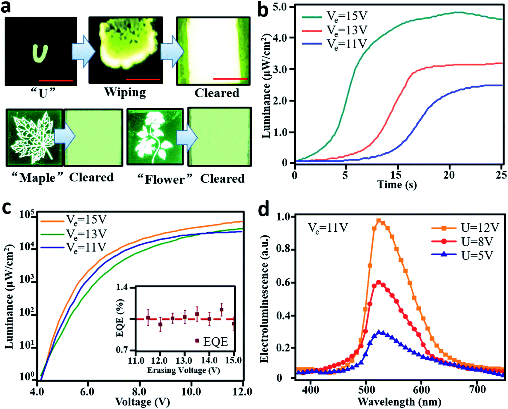 | ||
| Fig. 5 Wiping characteristics and device properties afterwards. (a), EL photos of the written letter “U”, “maple leaf” and “lily flower” before wiping, under wiping and after wiping. The device begins to “burn” from one end to the other end of the substrate until covering the entire substrates. (b) The luminance variation at the area without patterns versus time at different erasing voltages. The higher the erasing voltage, the faster the wiping, and the brighter the PeLED. (c) Relationship between luminance and applied voltage for devices swiped at 11 V, 13 V and 15 V. No obvious difference is found in turn-on voltage, response time and saturation level among the three curves. The inset demonstrates the EQE variation based on the wiping voltage. (d) Emission spectrum of the devices at voltage of 5 V, 8 V and 12 V after wiping at 11 V. | ||
Except for the illuminated properties of the device, the stable properties and mechanical deformation for the flexible PeLED-based device are other considerable parameters in the application, as revealed in Fig. 6. First, the cycle test for the devices by two heating methods (contact heating and electric heating) were characterized, as shown in Fig. 6a and b. The flexible substrate suffers voltage on/off switch for 400 s and both of the devices displayed a stable EL intensity throughout the whole testament. The slightly lower EL intensity is due to lower EQE after wiping. Fig. 6c is the test of the bending substrate with patterns and electrical wiping under illumination. The maximum bending degree of the two treated WWPeLEDs are over 80° without any negative effect on the performance, indicating a great flexibility of the devices. Repeatability tests of the devices with patterns and electrical wiping under bending and no-bending substrates were carried out, as shown in Fig. 6d. The flexible devices are bended after 500 bending cycles while keeping devices under 80° bending as a control sample. Both of the devices present extremely stable performance by turning the devices on and off for over 100 times. It is worth noting that in the experiment, PET substrate was able to withstand the heating temperature from the heating pen and the heating mold due to the short heating time as well as the small contact area between the PET substrate and the heating pen. Wiping of the patterns on PLED is a one-step process. The wiped patterns cannot be rewritten or reprinted again on the device, as the crystallization of perovskites is not a reversible process. These results obviously prove the robustness of the WWPeLED devices in both mechanical and EL performance after a long period of operations, allowing for the reliable and practical applications.
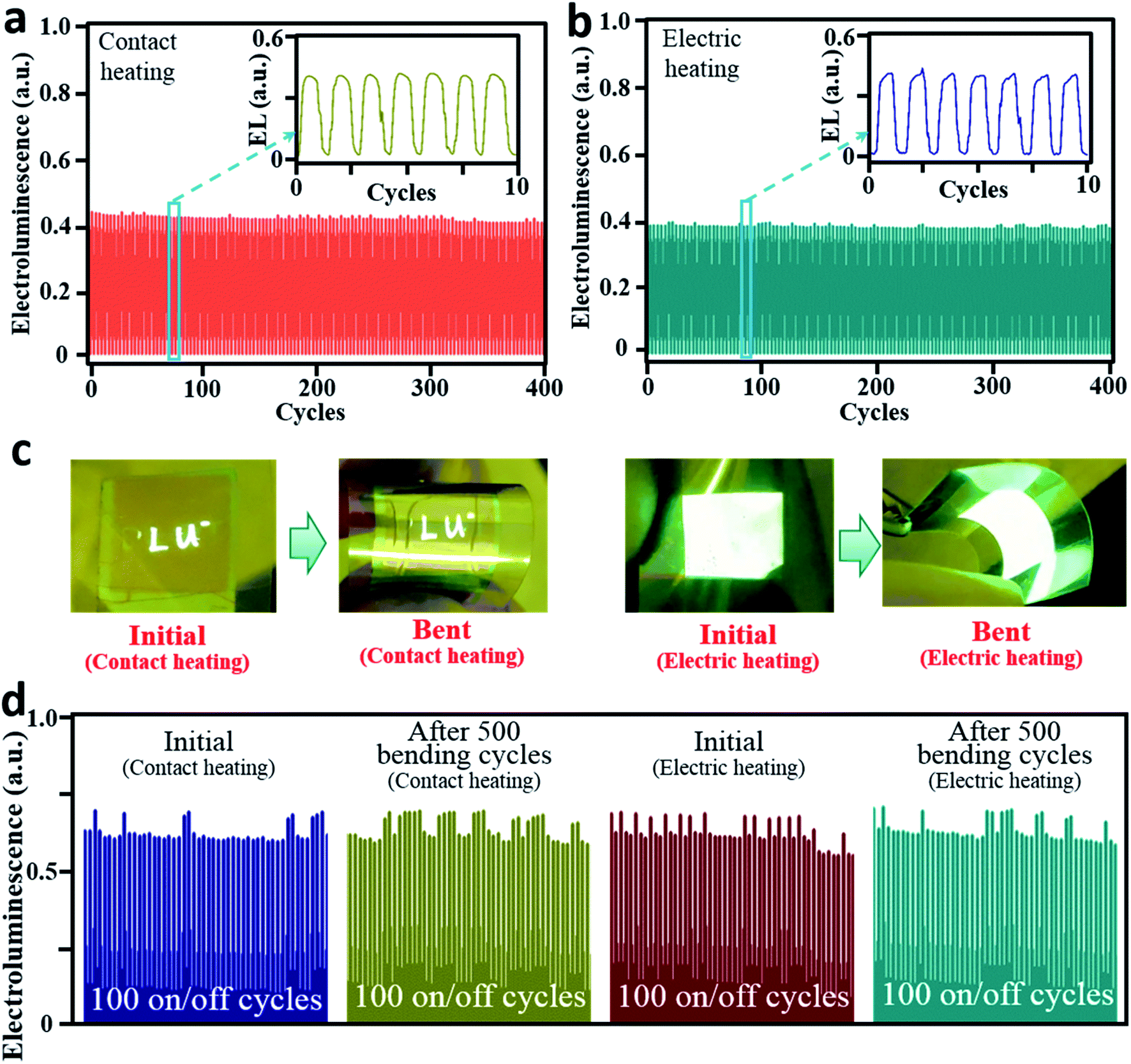 | ||
| Fig. 6 WWPeLED properties on the flexible substrate for stable and deformation tests. (a) Stability and repeatability test of contact heated WWPeLED devices turned on and off for 400 cycles. The EL intensity almost keeps constant throughout the entire time. (b) Stability and repeatability test of devices heated electrically for 400 cycles. The EL intensity still keeps unchanged but is slightly lower than that by contact heating in (a). (c) Flexibility test by bending devices with and without patterns. The bending degrees are over 80° for all the devices, demonstrating a constant light intensity during the bending process. (d) Flexibility robustness test for no bending and under bending devices with and without patterns. The EL intensity stays in a highly stable situation after 100 on/off cycles for both contact heating and electric heating, corresponding to the devices in (c). The bended devices are tested after 500 bending cycles, presenting exceedingly uniform performance in 100 on/off cycles for the two circumstances. | ||
3. Conclusion
In summary, we introduced a flexible WWPeLED device that utilizes a novel material treatment method for controlling the corresponding EQE at different positions and make the best use of the difference between low and high EQE regions to record personalized handwriting as well as thermal printing information. The low temperature prevents materials from crystallization while the high temperature facilitates the crystallization of the organic molecules, so that the crystalized part possesses a much smaller turn-on voltage, where over 5 V difference is found in the experiment. By heating up the desired area while keeping other regions cool, part of the PeLED to be lightened up can be precisely controlled. The wiped WWPeLED also shows a possible performance of removing the marks and switching as a regular lighting system. The excellent stability and repeatability of the flexible WWPeLED devices have also been evidenced with hundred times of bending and current on/off cycle test. Our WWPeLED devices may find prospective applications in electronic display, smart sensor networks and human–machine interfaces.4. Experiment
Experimental details are provided in the ESI.†Conflicts of interest
There are no conflicts to declare.Acknowledgements
This project is financially supported by National Natural Science Foundation of China (NSFC 62005035 and 51975101), Dalian University of Technology (DUT20JC01) and Dalian Science and Technology Bureau (2020JJ26GX047).References
- P. K. Challa, T. Kartanas, J. Charmet and T. P. J. Knowles, Microfluidic Devices Fabricated Using Fast Wafer-Scale LED-Lithography Patterning, Biomicrofluidics, 2017, 11(1), 014113 CrossRef PubMed.
- P. Wu, J. Guo, K. Jiang, J. Wang and L. Jiang, Direct Water-Writing/Electroerasing Pattern on PEDOT Inverse Opals, Adv. Funct. Mater., 2019, 29(38), 1808473 CrossRef.
- T. Zhang, H. Tang, S. Li, Z. Wen, X. Xiao, Y. Zhang, F. Wang, K. Wang and D. Wu, Highly Efficient Chip-Scale Package LED Based on Surface Patterning, IEEE Photon. Technol. Lett., 2017, 29(20), 1703–1706 Search PubMed.
- S. Y. Lee, S.-H. Kim, H. Hwang, J. Y. Sim and S.-M. Yang, Controlled Pixelation of Inverse Opaline Structures Towards Reflection-Mode Displays, Adv. Mater., 2014, 26(15), 2391–2397 CrossRef CAS PubMed.
- Y.-L. Tong, Y.-W. Zhang, K. Ma, R. Cheng, F. Wang and S. Chen, One-Step Synthesis of FA-Directing FAPbBr(3) Perovskite Nanocrystals toward High-Performance Display, ACS Appl. Mater. Interfaces, 2018, 10(37), 31603–31609 CrossRef CAS PubMed.
- N. Vogel, R. A. Belisle, B. Hatton, T.-S. Wong and J. Aizenberg, Transparency and Damage Tolerance of Patternable Omniphobic Lubricated Surfaces Based on Inverse Colloidal Monolayers, Nat. Commun., 2013, 4, 2176 CrossRef PubMed.
- K. Zhong, J. Li, L. Liu, S. Van Cleuvenbergen, K. Song and K. Clays, Instantaneous, Simple, and Reversible Revealing of Invisible Patterns Encrypted in Robust Hollow Sphere Colloidal Photonic Crystals, Adv. Mater., 2018, 30(25), 201707246 CrossRef PubMed.
- Y. Zhao, X. Zhao, C. Sun, J. Li, R. Zhu and Z. Gu, Encoded Silica Colloidal Crystal Beads as Supports for Potential Multiplex Immunoassay, Anal. Chem., 2008, 80(5), 1598–1605 CrossRef CAS PubMed.
- B. Zhu, Q. Fu, K. Chen and J. Ge, Liquid Photonic Crystals for Mesopore Detection, Angew. Chem., Int. Ed., 2018, 57(1), 252–256 CrossRef CAS PubMed.
- M. Malekmohammad, M. Soltanolkotabi, R. Asadi, M. H. Naderi, A. Erfanian, M. Zahedinejad, S. Bagheri and M. Khaje, Hybrid Structure for Efficiency Enhancement of Photodetectors, Appl. Surf. Sci., 2013, 264, 1–6 CrossRef CAS.
- L. Shang, Y. Yu, W. Gao, Y. Wang, L. Qu, Z. Zhao, R. Chai and Y. Zhao, Bio-Inspired Anisotropic Wettability Surfaces from Dynamic Ferrofluid Assembled Templates, Adv. Funct. Mater., 2018, 28(7), 201705802 CrossRef.
- S. Bi, Q. Li, Z. He, Q. Guo, K. Asare-Yeboah, Y. Liu and C. Jiang, Highly Enhanced Performance of Integrated Piezo Photo-Transistor with Dual Inverted OLED Gate and Nanowire Array Channel, Nano Energy, 2019, 66, 104101 CrossRef CAS.
- H. J. Bae, S. Bae, C. Park, S. Han, J. Kim, L. N. Kim, K. Kim, S.-H. Song, W. Park and S. Kwon, Biomimetic Microfingerprints for Anti-Counterfeiting Strategies, Adv. Mater., 2015, 27(12), 2083–2089 CrossRef CAS PubMed.
- D. Yang, Y. Qin, S. Ye and J. Ge, Polymerization-Induced Colloidal Assembly and Photonic Crystal Multilayer for Coding and Decoding, Adv. Funct. Mater., 2014, 24(6), 817–825 CrossRef CAS.
- T. Sarkar, K. Selvakumar, L. Motiei and D. Margulies, Message in a molecule, Nat. Commun., 2016, 7, 11374 CrossRef CAS PubMed.
- K. Macrakis, E. K. Bell, D. L. Perry and R. D. Sweeder, Invisible Ink Revealed: Concept, Context, and Chemical Principles of "Cold War" Writing, J. Chem. Educ., 2012, 89(4), 529–532 CrossRef CAS.
- T. R. Hebner, C. C. Wu, D. Marcy, M. H. Lu and J. C. Sturm, Ink-Jet Printing of Doped Polymers for Organic Light Emitting Devices, Appl. Phys. Lett., 1998, 72(5), 519–521 CrossRef CAS.
- P. F. Tian, V. Bulovic, P. E. Burrows, G. Gu, S. R. Forrest and T. X. Zhou, Precise, Scalable Shadow Mask Patterning of Vacuum-Deposited Organic Light Emitting Devices, J. Vac. Sci. Technol., A, 1999, 17(5), 2975–2981 CrossRef CAS.
- J. A. DeFranco, B. S. Schmidt, M. Lipson and G. G. Malliaras, Photolithographic Patterning of Organic Electronic Materials, Org. Electron., 2006, 7(1), 22–28 CrossRef CAS.
- J. Huang, R. Xia, Y. Kim, X. Wang, J. Dane, O. Hofmann, A. Mosley, A. J. de Mello, J. C. de Mello and D. D. C. Bradley, Patterning of Organic Devices by Interlayer Lithography, J. Mater. Chem., 2007, 17(11), 1043–1049 RSC.
- S. C. Chang, J. Bharathan, Y. Yang, R. Helgeson, F. Wudl, M. B. Ramey and J. R. Reynolds, Dual-Color Polymer Light-Emitting Pixels Processed by Hybrid Inkjet Printing, Appl. Phys. Lett., 1998, 73(18), 2561–2563 CrossRef CAS.
- P. F. Tian, P. E. Burrows and S. R. Forrest, Photolithographic Patterning of Vacuum-Deposited Organic Light Emitting Devices, Appl. Phys. Lett., 1997, 71(22), 3197–3199 CrossRef CAS.
- D. G. Lidzey, M. A. Pate, M. S. Weaver, T. A. Fisher and D. D. C. Bradley, Photoprocessed and Micropatterned Conjugated Polymer LEDs, Synth. Met., 1996, 82(2), 141–148 CrossRef CAS.
- C.-Y. Chang, F.-Y. Tsai, S.-J. Jhuo and M.-J. Chen, Enhanced OLED Performance Upon Photolithographic Patterning by Using an Atomic-Layer-Deposited Buffer Layer, Org. Electron., 2008, 9(5), 667–672 CrossRef CAS.
- S. Bi, Q. Li, Y. Yan, K. Asare-Yeboah, T. Ma, C. Tang, Z. Ouyang, Z. He, Y. Liu and C. Jiang, Layer-Dependent Anisotropic Frictional Behavior in Two-Dimensional Monolayer Hybrid Perovskite/ITO Layered Heterojunctions, Phys. Chem. Chem. Phys., 2019, 21(5), 2540–2546 RSC.
- J. Chen, J. Wang, X. Xu, J. Li, J. Song, S. Lan, S. Liu, B. Cai, B. Han, J. T. Precht, D. Ginger and H. Zeng, Efficient and Bright White Light-Emitting Diodes Based on Single-Layer Heterophase Halide Perovskites, Nat. Photonics, 2021, 15(3), 238–244 CrossRef CAS.
- J. Song, J. Li, L. Xu, J. Li, F. Zhang, B. Han, Q. Shan and H. Zeng, Room-Temperature Triple-Ligand Surface Engineering Synergistically Boosts Ink Stability, Recombination Dynamics, and Charge Injection toward EQE-11.6% Perovskite QLEDs, Adv. Mater., 2018, 30(30), 1800764 CrossRef PubMed.
- K. Lin, J. Xing, L. N. Quan, F. P. G. de Arquer, X. Gong, J. Lu, L. Xie, W. Zhao, D. Zhang, C. Yan, W. Li, X. Liu, Y. Lu, J. Kirman, E. H. Sargent, Q. Xiong and Z. Wei, Perovskite Light-Emitting Diodes with External Quantum Efficiency Exceeding 20 Percent, Nature, 2018, 562(7726), 245–248 CrossRef CAS PubMed.
- Y.-H. Kim, S. Kim, A. Kakekhani, J. Park, J. Park, Y.-H. Lee, H. Xu, S. Nagane, R. B. Wexler, D.-H. Kim, S. H. Jo, L. Martinez-Sarti, P. Tan, A. Sadhanala, G.-S. Park, Y.-W. Kim, B. Hu, H. J. Bolink, S. Yoo, R. H. Friend, A. M. Rappe and T.-W. Lee, Comprehensive Defect Suppression in Perovskite Nanocrystals for High-Efficiency Light-Emitting Diodes, Nat. Photonics, 2021, 15(2), 148–155 CrossRef CAS.
- Y. Dong, Y.-K. Wang, F. Yuan, A. Johnston, Y. Liu, D. Ma, M.-J. Choi, B. Chen, M. Chekini, S.-W. Baek, L. K. Sagar, J. Fan, Y. Hou, M. Wu, S. Lee, B. Sun, S. Hoogland, R. Quintero-Bermudez, H. Ebe, P. Todorovic, F. Dinic, P. Li, H. T. Kung, M. I. Saidaminov, E. Kumacheva, E. Spiecker, L.-S. Liao, O. Voznyy, Z.-H. Lu and E. H. Sargent, Bipolar-Shell Resurfacing for Blue LEDs Based on Strongly Confined Perovskite Quantum Dots, Nat. Nanotechnol., 2020, 15(8), 668–674 CrossRef CAS PubMed.
- Y.-K. Wang, F. Yuan, Y. Dong, J.-Y. Li, A. Johnston, B. Chen, M. I. Saidaminov, C. Zhou, X. Zheng, Y. Hou, K. Bertens, H. Ebe, D. Ma, Z. Deng, S. Yuan, R. Chen, L. K. Sagar, J. Liu, J. Fan, P. Li, X. Li, Y. Gao, M.-K. Fung, Z.-H. Lu, O. M. Bakr, L.-S. Liao and E. H. Sargent, All-Inorganic Quantum-Dot LEDs Based on a Phase-Stabilized alpha-CsPbI3 Perovskite, Angew. Chem., Int. Ed., 2021, 60(29), 16164–16170 CrossRef CAS PubMed.
- F.-S. Zu, P. Amsalem, I. Salzmann, R.-B. Wang, M. Ralaiarisoa, S. Kowarik, S. Duhm and N. Koch, Impact of White Light Illumination on the Electronic and Chemical Structures of Mixed Halide and Single Crystal Perovskites, Adv. Opt. Mater., 2017, 5(9), 201700139 Search PubMed.
- T. G. Ryan and P. D. Calvert, Diffusion and Annealing in Crystallizing Polymers, Polymer, 1982, 23(6), 877–883 CrossRef CAS.
- J.-H. Huang, C.-Y. Yang, Z.-Y. Ho, D. Kekuda, M.-C. Wu, F.-C. Chien, P. Chen, C.-W. Chu and K.-C. Ho, Annealing Effect of Polymer Bulk Heterojunction Solar Cells Based on Polyfluorene and Fullerene Blend, Org. Electron., 2009, 10(1), 27–33 CrossRef CAS.
- J.-w. Chen, J. Dai, J.-h. Yang, N. Zhang, T. Huang, Y. Wang and C.-l. Zhang, Annealing Induced Microstructure and Mechanical Property Changes of Impact Resistant Polypropylene Copolymer, Chin. J. Polym. Sci., 2015, 33(9), 1211–1224 CrossRef CAS.
- Q. Meng, Y. Chen, Y. Y. Xiao, J. Sun, X. Zhang, C. B. Han, H. Gao, Y. Zhang and H. Yan, Effect of Temperature on The Performance of Perovskite Solar Cells, J. Mater. Sci. Mater. Electron., 2021, 32(10), 12784–12792 CrossRef CAS.
- T. Moot, J. B. Patel, G. McAndrews, E. J. Wolf, D. Morales, I. E. Gould, B. A. Rosales, C. C. Boyd, L. M. Wheeler, P. A. Parilla, S. W. Johnston, L. T. Schelhas, M. D. McGehee and J. M. Luther, Temperature Coefficients of Perovskite Photovoltaics for Energy Yield Calculations, ACS Energy Lett., 2021, 6(5), 2038–2047 CrossRef CAS.
- M. G. Goesten and R. Hoffmann, Mirrors of Bonding in Metal Halide Perovskites, J. Am. Chem. Soc., 2018, 140(40), 12996–13010 CrossRef CAS PubMed.
- J. S. Manser, M. I. Saidaminov, J. A. Christians, O. M. Bakr and P. V. Kamat, Making and Breaking of Lead Halide Perovskites, Acc. Chem. Res., 2016, 49(2), 330 CrossRef CAS PubMed.
Footnote |
| † Electronic supplementary information (ESI) available. See DOI: 10.1039/d1na00465d |
| This journal is © The Royal Society of Chemistry 2021 |