
 Open Access Article
 This Open Access Article is licensed under a Creative Commons Attribution-Non Commercial 3.0 Unported Licence
Doping-free bandgap tunability in Fe2O3 nanostructured films†
Sujit A.
Kadam
a,
Giang Thi
Phan
 a,
Duy Van
Pham
*ab,
Ranjit A.
Patil
a,
Chien-Chih
Lai
a,
Yan-Ruei
Chen
c,
Yung
Liou
c and
Yuan-Ron
Ma
*a
a,
Duy Van
Pham
*ab,
Ranjit A.
Patil
a,
Chien-Chih
Lai
a,
Yan-Ruei
Chen
c,
Yung
Liou
c and
Yuan-Ron
Ma
*a
aDepartment of Physics, National Dong Hwa University, Hualien 97401, Taiwan. E-mail: duypham0611@gmail.com; ronma@mail.ndhu.edu.tw
bCenter for Condensed Matter Sciences, National Taiwan University, Taipei 10617, Taiwan
cInstitute of Physics, Academia Sinica, Taipei 11529, Taiwan
First published on 29th July 2021
Abstract
A tunable bandgap without doping is highly desirable for applications in optoelectronic devices. Herein, we develop a new method which can tune the bandgap without any doping. In the present research, the bandgap of Fe2O3 nanostructured films is simply tuned by changing the synthesis temperature. The Fe2O3 nanostructured films are synthesized on ITO/glass substrates at temperatures of 1100, 1150, 1200, and 1250 °C using the hot filament metal oxide vapor deposition (HFMOVD) and thermal oxidation techniques. The Fe2O3 nanostructured films contain two mixtures of Fe2+ and Fe3+ cations and two trigonal (α) and cubic (γ) phases. The increase of the Fe2+ cations and cubic (γ) phase with the elevated synthesis temperatures lifted the valence band edge, indicating a reduction in the bandgap. The linear bandgap reduction of 0.55 eV without any doping makes the Fe2O3 nanostructured films promising materials for applications in bandgap engineering, optoelectronic devices, and energy storage devices.
Introduction
The bandgap is a fundamental parameter when selecting a material for various electronic and optoelectronic device applications as it governs the electronic transport and light–matter interaction properties. In the current research on optoelectronic materials, it is highly desirable to be able to tune the bandgap for developing highly efficient solar cells1–3 or enhancing the performance of LEDs and photodetectors.4–6 To achieve the desired bandgap for specific applications, doping has been considered as an effective method to tune the bandgap of semiconductors because it can form localized states in the bandgap;7–10 however, the intrinsic optical and electrical properties of host materials can be affected.10,11 Recently, some promising methods have been developed for tuning the bandgap of semiconducting materials without doping, such as strain engineering,12,13 thickness control,14,15 and synthesis temperature control.11,16 Bandgap tuning without any doping will be a very powerful advantage for applications in bandgap engineering and optoelectronic devices. The bandgap tuning possibility of semiconductors can be classified into three types. In the first type of bandgap tuning, the highest energy level of the valence band (VB) does not change, while the lowest energy level of the conduction band (CB) is lowered. In the second type of bandgap tuning, the highest energy level of the VB is lifted, while the lowest energy level of the CB remains unchanged. The highest energy level of the VB and lowest energy level of the CB are raised and lowered, respectively, in the third type of bandgap tuning. The schematic illustration in Fig. 1 shows the three types of bandgap tuning. The bandgaps before and after tuning of the direct and indirect bandgap semiconductors are shown in Fig. 1a and b, respectively.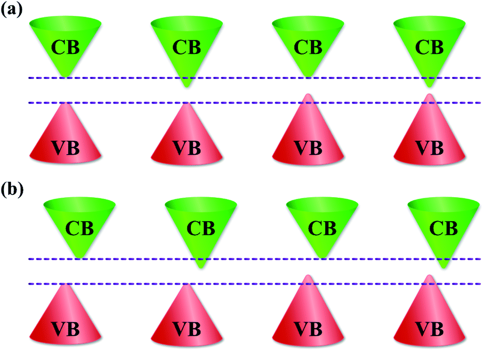 | ||
| Fig. 1 Types of bandgap tuning. Bandgap before and after tuning for (a) direct and (b) indirect bandgap semiconductors. The bandgap tuning possibility can be classified into three types: (1) the highest levels of the VB remain, while the lowest levels of the CB are lowered; (2) the highest levels of the VB are raised, while the lowest levels of the CB remain unchanged; (3) the highest levels of the VB and the lowest level of the CB are raised and lowered, respectively. | ||
Metal oxides with a wide bandgap are excellent candidates for use in optoelectronic devices.17,18 Among the numerous metal oxides, iron oxide is an interesting material due to its multiple oxidation states and stability of crystal phases, such as FeO,19,20 Fe3O4,21,22 Fe7O9,23 α-Fe2O3,24,25 β-Fe2O3,26,27 and γ-Fe2O3.28,29 Iron oxide is widely used in a wide range of applications in nanodevices due to its unique properties, such as water splitting,24,25,30 supercapacitors,31–33 lithium-ion batteries,34–36 catalysts,37–39 photodetectors,40 and gas sensors.41–43 In our proposed approach, we synthesized Fe2O3 nanostructured films on ITO/glass substrates at various synthesis temperatures. The results show that Fe2O3 nanostructured films contain two mixtures of Fe2+ and Fe3+ cations and two trigonal (α) and cubic (γ) phases. The increase of the Fe2+ cations and cubic (γ) phase in Fe2O3 nanostructured films with the elevated synthesis temperatures plays a critical role in tuning the bandgap of the Fe2O3 nanostructured films. The linear reduction in the bandgap from 1.65 to 1.10 eV without any doping of Fe2O3 nanostructured films provides a uniquely controllable route and makes it a promising candidate for applications in bandgap engineering, optoelectronic devices, and energy storage devices.
Experimental section
Synthesis of Fe2O3 nanostructured films
A larger area of FeOx nanostructures was synthesized on ITO/glass (ρ ∼ 8 Ω sq−1) substrates using the HFMOVD technique. The HFMOVD technique is an important deposition method that allows the controllable synthesis of 1D metal-oxide nanostructures with different forms.11,16,44–48 By only control of the synthesis temperature, the metals with multiple oxidation states can form the non-stoichiometric metal oxide nanostructures, which contain the phase combination and cation mixture.11,16 This leads to a change in the bandgap of the metal oxide nanostructures without any doping with other metals, suggesting that the HFMOVD technique is suitable for bandgap engineering. Clean pure Fe wires (99.9%) with a diameter of ∼1 mm were fixed between two copper (Cu) electrodes in the chamber. After the pressure of the vacuum chamber was pumped down and maintained at 0.3 Torr, the Fe wires were heated to 1100, 1150, 1200, and 1250 °C for 30 min to sublimate hot Fe vapor. The residual oxygen in the chamber reacted with the hot Fe vapor to form iron oxide vapor. The iron oxide vapor immediately condensed to form Fe3O4 and metallic Fe nanostructures on the ITO/glass substrate, which was placed at a distance of ∼4 mm above the Fe wire. The Fe3O4 and metallic Fe nanostructures were then annealed and oxidized to produce Fe2O3 nanostructured films in a controlled O2 atmosphere of ∼500 Torr at a temperature of 500 °C for 4 hours in a quartz tube furnace.Characterization of the Fe2O3 nanostructured films
The morphological features of the Fe2O3 nanostructured films were observed using a field emission scanning electron microscope (FESEM, JEOL JSM-6500F). The crystalline phase of the Fe2O3 nanostructured films was confirmed using an X-ray diffractometer (XRD, PANalytical X'Pert PRO). Crystalline analysis of the Fe2O3 nanostructured films was performed using a transmission electron microscope (TEM, JEOL JEM-2100) at an accelerating voltage of 200 kV. The simulated electron diffraction patterns were recorded using crystallographic software (Carine Crystallography version 3.1). The electronic structures and quantitative elemental information of the Fe2O3 nanostructured films were examined using an X-ray photoelectron spectrometer (XPS, Thermo Scientific Inc., K-alpha) with a microfocus monochromatic Al Kα X-ray source. The optical transmittance and absorbance of the Fe2O3 nanostructured films were studied using a spectrophotometer (Ocean Optics DH-2000-BAL) with an ITO/glass substrate as a reference.Results and discussion
The FESEM images in Fig. 2a–d show the side views of the large-area arrays of the Fe2O3 nanostructured films synthesized at various temperatures. The Fe2O3 nanostructured films are produced by the thermal oxidation of Fe3O4 and metallic Fe nanostructures, which are synthesized at temperatures of 1100, 1150, 1200, and 1250 °C. For convenience, the Fe2O3 nanostructured films synthesized at the various temperatures are denoted as Fe2O3 nanostructured films@1100, 1150, 1200, and 1250 °C, respectively. Clearly, the sample@1100 °C is just the thin film, while the samples@1150, 1200, and 1250 °C not only possess thick buffer layers but also nanofibers and nanosheets, which are grown on the buffer layers, as shown in Fig. S1 (ESI†). The nanofibers and nanosheets are only formed on the samples@1150, 1200, and 1250 °C. This can be attributed to the presence of metallic iron in these samples before annealing. The existence of metallic iron has been confirmed by the XRD patterns, as shown in Fig. S2 (ESI†). During thermal oxidation, metallic iron reacts with the oxygen gas to increase the thickness of the Fe2O3 buffer layer as well as forming the Fe2O3 nanofibers and sheets. The average thickness of the Fe2O3 buffer layers increases from ∼116 to ∼3319 nm with elevated synthesis temperatures.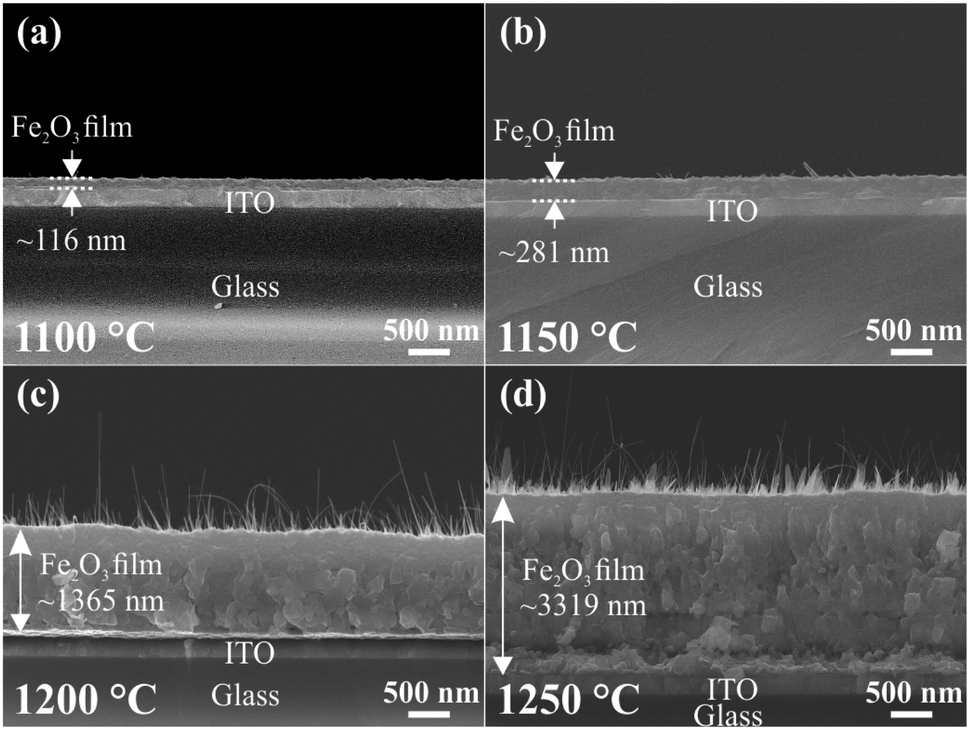 | ||
| Fig. 2 Surface morphology. (a–d) FESEM images showing the side view of the Fe2O3 nanostructured films@1100, 1150, 1200, and 1250 °C. The average thickness of the Fe2O3 thin film increases from ∼116 to ∼3319 nm with the elevated synthesis temperatures. | ||
The crystalline phase of the Fe2O3 nanostructured films is analyzed by XRD and HRTEM measurements, and the results are shown in Fig. 3. The XRD patterns of ITO coated on the glass substrate and Fe2O3 nanostructured films@1100, 1150, 1200, and 1250 °C are displayed in Fig. 3a. For the Fe2O3 nanostructured films@1150, 1200, and 1250 °C, all the diffraction peaks reveal that the Fe2O3 nanostructured films contain two crystals together, which are the trigonal (α) phase and the cubic (γ) phase. Meanwhile, the observed diffraction pattern of the Fe2O3 thin film@1100 °C corresponds to all diffraction peaks of the trigonal (α) phase. The trigonal (α) crystal structure possesses a space group of R![[3 with combining macron]](https://www.rsc.org/images/entities/char_0033_0304.gif) c with lattice constants of a = b = 0.5021 nm, c = 1.372 nm, α = β = 90° and γ = 120° (ICSD 201097), while the cubic (γ) crystal structure has a space group of P4332 with lattice constants of a = b = c = 0.8346 nm and α = β = γ = 90° (ICSD 87119). According to the Rietveld refinement results, the crystal composition percentage of the cubic (γ) phase increases linearly from 0 to ∼23.7% with the elevated synthesis temperatures, as shown in Fig. S3 (ESI†). The trigonal (α) and cubic (γ) phases of the Fe2O3 nanostructured films have also been confirmed by TEM images. Fig. 3b–j show the single nanosheet and nanowire, high-resolution TEM (HRTEM) images, the selected area electron diffraction (SAED) patterns, and the simulated electron diffraction (SED) patterns of the Fe2O3 nanostructured films@1250 °C. Fig. 3b–d show the low- and high-resolution TEM images, and the SAED patterns of the 2D Fe2O3 nanosheets. The only interplanar atomic spacing of 0.25 nm is found in the HRTEM in Fig. 3c, which is indexed to the (110) plane in the trigonal (α) phase. The SED patterns with a [001] zone axis in Fig. 3k are consistent with the SAED pattern in Fig. 3d, indicating that the 2D Fe2O3 nanosheets possess only the trigonal (α) phase. Fig. 3e–g show the low- and high-resolution TEM images, and the SAED patterns of the 1D Fe2O3 nanofibers. The HRTEM in Fig. 3f reveals that the 1D Fe2O3 nanofibers contain both trigonal (α) and cubic (γ) phases. The interplanar atomic spacings of 0.25 and 0.37 nm correspond to the (110) and (012) planes in the trigonal (α) phase, while the interplanar atomic spacings of 0.25 and 0.29 nm are consistent with the (113) and (022) planes in the cubic (γ) phase. Fig. 3h and i show the SED patterns for the trigonal (α) and cubic (γ) phases with the [2
c with lattice constants of a = b = 0.5021 nm, c = 1.372 nm, α = β = 90° and γ = 120° (ICSD 201097), while the cubic (γ) crystal structure has a space group of P4332 with lattice constants of a = b = c = 0.8346 nm and α = β = γ = 90° (ICSD 87119). According to the Rietveld refinement results, the crystal composition percentage of the cubic (γ) phase increases linearly from 0 to ∼23.7% with the elevated synthesis temperatures, as shown in Fig. S3 (ESI†). The trigonal (α) and cubic (γ) phases of the Fe2O3 nanostructured films have also been confirmed by TEM images. Fig. 3b–j show the single nanosheet and nanowire, high-resolution TEM (HRTEM) images, the selected area electron diffraction (SAED) patterns, and the simulated electron diffraction (SED) patterns of the Fe2O3 nanostructured films@1250 °C. Fig. 3b–d show the low- and high-resolution TEM images, and the SAED patterns of the 2D Fe2O3 nanosheets. The only interplanar atomic spacing of 0.25 nm is found in the HRTEM in Fig. 3c, which is indexed to the (110) plane in the trigonal (α) phase. The SED patterns with a [001] zone axis in Fig. 3k are consistent with the SAED pattern in Fig. 3d, indicating that the 2D Fe2O3 nanosheets possess only the trigonal (α) phase. Fig. 3e–g show the low- and high-resolution TEM images, and the SAED patterns of the 1D Fe2O3 nanofibers. The HRTEM in Fig. 3f reveals that the 1D Fe2O3 nanofibers contain both trigonal (α) and cubic (γ) phases. The interplanar atomic spacings of 0.25 and 0.37 nm correspond to the (110) and (012) planes in the trigonal (α) phase, while the interplanar atomic spacings of 0.25 and 0.29 nm are consistent with the (113) and (022) planes in the cubic (γ) phase. Fig. 3h and i show the SED patterns for the trigonal (α) and cubic (γ) phases with the [2![[2 with combining macron]](https://www.rsc.org/images/entities/char_0032_0304.gif) 1] and [21
1] and [21![[1 with combining macron]](https://www.rsc.org/images/entities/char_0031_0304.gif) ] zone axes, respectively. When the two SED patterns are completely overlapped, as shown in Fig. 3j, the superposed SED patterns match well with the SAED pattern in Fig. 3g, confirming that the 1D Fe2O3 nanofibers consist of the two trigonal (α) and cubic (γ) phases. Similar to 2D Fe2O3 nanosheets, the 2D Fe2O3 thin film@1100 °C contains only the trigonal (α) phase with an interplanar atomic spacing of 0.25 nm, which corresponds to the (110) plane. The low- and high-resolution TEM images and the SAED patterns of the 2D Fe2O3 thin film@1100 °C are shown in Fig. S4 (ESI†). The XRD and TEM results indicate that the cubic (γ) phase is only formed at temperatures higher than 1100 °C.
] zone axes, respectively. When the two SED patterns are completely overlapped, as shown in Fig. 3j, the superposed SED patterns match well with the SAED pattern in Fig. 3g, confirming that the 1D Fe2O3 nanofibers consist of the two trigonal (α) and cubic (γ) phases. Similar to 2D Fe2O3 nanosheets, the 2D Fe2O3 thin film@1100 °C contains only the trigonal (α) phase with an interplanar atomic spacing of 0.25 nm, which corresponds to the (110) plane. The low- and high-resolution TEM images and the SAED patterns of the 2D Fe2O3 thin film@1100 °C are shown in Fig. S4 (ESI†). The XRD and TEM results indicate that the cubic (γ) phase is only formed at temperatures higher than 1100 °C.
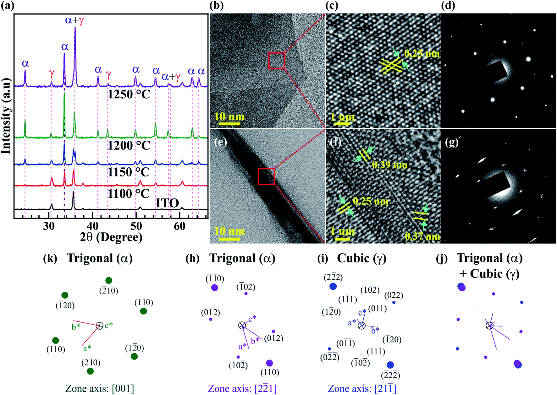 | ||
| Fig. 3 Crystal structure determination. (a) XRD spectra of the ITO/glass substrates and the Fe2O3 nanostructured films@1100, 1150, 1200, and 1250 °C. Fe2O3 nanostructured films contain two crystal structures of the trigonal (α) phase and cubic (γ) phase. (b–g) Single nanosheet, single nanowire, HRTEM, and SAED patterns of the Fe2O3 nanostructured films@1250 °C. (h–k) Simulated electron diffraction patterns of trigonal (α) and cubic (γ) phases with various zone axes. TEM results confirm the existence of the cubic (γ) phase in nanofibers. | ||
The chemical compositions and electronic structures of the Fe2O3 nanostructured films were further identified by X-ray photoelectron spectroscopy (XPS). The XPS spectra for Fe2O3 nanostructured films@1100, 1150, 1200, and 1250 °C are shown in Fig. 4a–e. All the XPS spectra of the Fe-2p core-level in Fig. 4a–d are decomposed further into four peaks at binding energies of ∼709.67, ∼722.90, ∼710.57, and ∼724.14 eV, assigned to Fe2+ 2p3/2, Fe2+ 2p1/2, Fe3+ 2p3/2, and Fe3+ 2p1/2, respectively. In addition to the double peaks of Fe 2p3/2 and Fe 2p1/2, the XPS spectra show the presence of two satellite (S1 and S2) and two surface (Sp1 and Sp2) peaks. The binding energies of the Fe-2p core-level agreed well with the previous reports.49–51 Obviously, the Fe2O3 nanostructured films@1100, 1150, 1200, and 1250 °C contain two Fe2+ and Fe3+ cations. According to quantitative XPS results, the amount of Fe2+ cations increases linearly from ∼6.11 to ∼13.5% with the elevated synthesis temperatures, as shown in Fig. 4e. In addition, the increase of Fe2+ cations is also confirmed using the energy-dispersive X-ray spectroscopy (EDS) line profile, as shown in Fig. S5 (ESI†). The Fe/O ratio increases linearly with increasing distance, indicating that the closer we get to the interface between the Fe2O3 film and ITO substrate, the higher the amount of Fe2+ cations. The combination of the trigonal (α) and cubic (γ) phases and the two mixtures of the Fe2+ and Fe3+ cations may cause impacts on the bandgap of the Fe2O3 nanostructured films. Fig. 4f shows the photoluminescence (PL) spectra of the Fe2O3 nanostructured films@1100, 1150, 1200, and 1250 °C. All the PL spectra were recorded in the wavelength range from 300 to 1000 nm. However, no PL peaks are observed in this region, indicating that the Fe2O3 nanostructured films have an indirect bandgap.
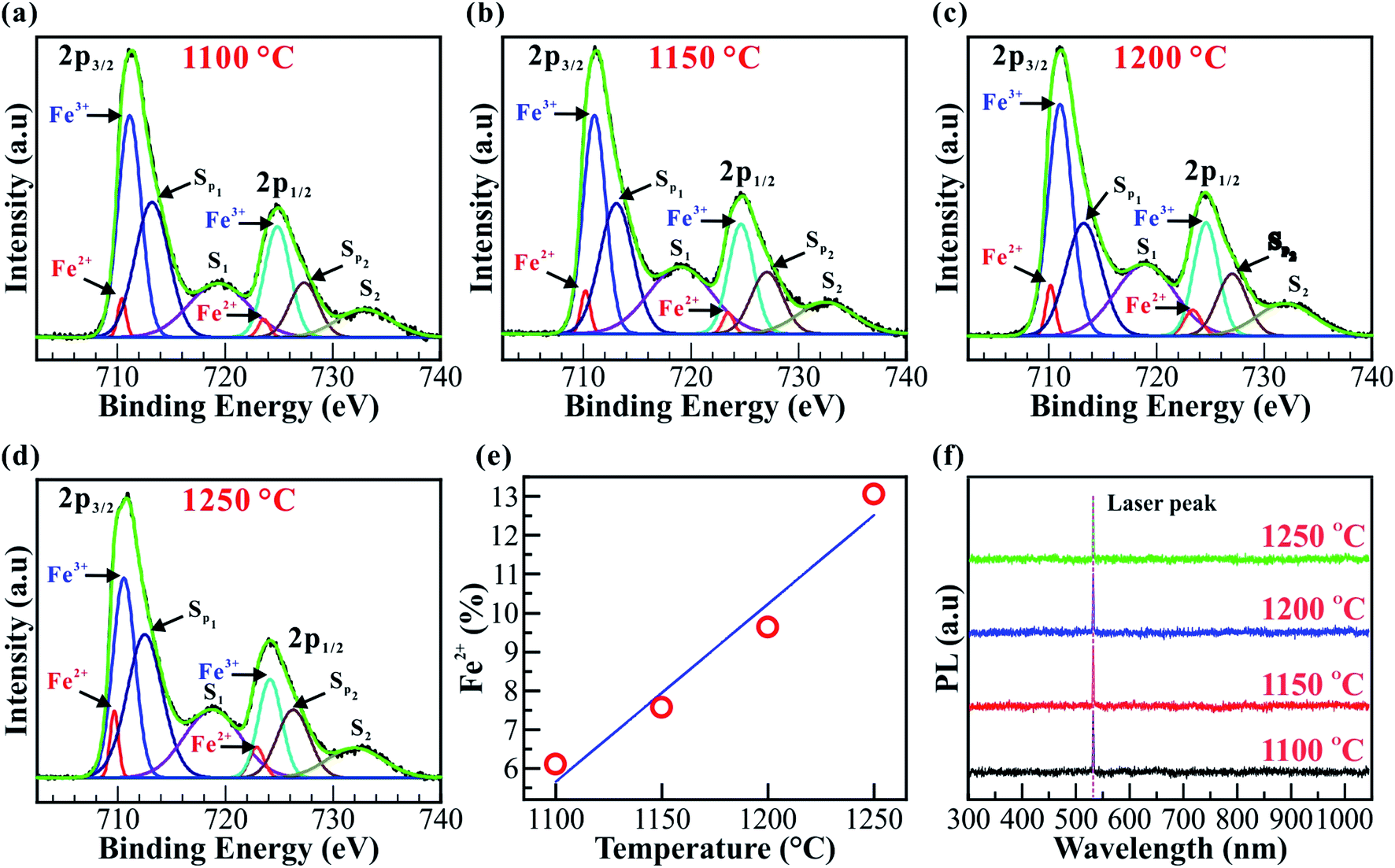 | ||
| Fig. 4 Chemical and photoluminescence (PL) analysis. (a–d) XPS spectra of the Fe2O3 nanostructured films. All the XPS spectra consist of Fe2+ 2p3/2, Fe3+ 2p3/2, Fe2+ 2p1/2, Fe3+ 2p1/2, surface and satellite peaks. (e) The linear graphs show the increase of the Fe2+ cations from ∼6.11 to ∼13.5% with the elevation of synthesis temperature, respectively. (f) PL spectra of the Fe2O3 nanostructured films@1100, 1150, 1200, and 1250 °C. No PL peaks are observed in the range from 300 to 1000 nm, indicating that the Fe2O3 nanostructured films have an indirect bandgap. | ||
Optical spectroscopy was used to investigate the bandgap reduction of the Fe2O3 nanostructured films. Fig. 5 shows the photographs, transmittance, and absorbance spectra, and the bandgap of the Fe2O3 nanostructured films@1100, 1150, 1200, and 1250 °C on the ITO/glass substrates. The photographs in Fig. 5a show the color of Fe2O3 nanostructured films, which changes from orange to deep red with elevated synthesis temperatures. The change in color of Fe2O3 nanostructured films is expected to produce a variety of absorbance and transmittance spectra. Fig. 5b and c show the transmittance and absorbance spectra for the Fe2O3 nanostructured films@1100, 1150, 1200, and 1250 °C in the wavelength range from 250 to 1000 nm. Clearly, the minimum transmittance for each spectrum is less than 1%, occurs at a wavelength of ∼315 nm, and extends to wavelengths of ∼364, ∼415, ∼513, and ∼610 nm for the nanostructured films@1100, 1150, 1200, and 1250 °C, respectively. As a result, the maximum absorbance for each spectrum of the Fe2O3 nanostructured films is increasingly broadened and the absorbance edge shifts towards longer wavelengths with the elevated synthesis temperatures. The red-shift of the absorbance edge is strongly related to the narrowing of the bandgap in the Fe2O3 nanostructured films. The indirect bandgap (Eg) of the Fe2O3 nanostructured films can be determined using the Tauc equation αhν = A(hν − Eg)2,52 where α is the absorption coefficient, h is Planck's constant, ν is the frequency of the incident light, and A is a constant. The absorbance spectra in Fig. 5c were transformed into the Tauc plot, as shown in Fig. 5d. Using the extrapolation method, the value of the bandgap (Eg) is determined as the intersection of the fitting dotted straight lines and hν axis. Therefore, the bandgaps of Fe2O3 nanostructured films@1100, 1150, 1200, and 1250 °C are 1.65, 1.58, 1.34, and 1.10 eV, respectively. The graph in Fig. 5e shows the temperature dependence of the bandgap of Fe2O3 nanostructured films. A linear fit between the bandgap values versus synthesis temperature indicates that the bandgap (Eg) of the Fe2O3 nanostructured films reduces linearly with the elevated synthesis temperatures. The linear bandgap reduction of 0.55 eV is due to the gain in the Fe2+ cations, the cubic (γ) phase in the Fe2O3 nanostructured films, and the thickness of the Fe2O3 nanostructured films. However, the influence of thickness on the bandgap reduction of the Fe2O3 nanostructured films is only ∼0.11 eV, as shown in Fig. S6–S9 (ESI†). The influence of the ITO/glass substrate on the optical properties of the Fe2O3 nanostructured films is also negligible (see Fig. S10, ESI†). The phase combination and cation mixture create structural disorder, leading to the formation of localized states. To determine the structural disorder of the Fe2O3 nanostructured films, the Urbach energy (Eu) was used for investigation purposes (see Fig. S11, ESI†). The linear increase of the Eu from 0.288 to 0.594 eV indicates the increase of localized states, leading to a significant bandgap reduction of the Fe2O3 nanostructured films. In addition, the bandgap reduction due to gain in metal cations and phase mixing has been demonstrated in previous studies.11,16 The bandgap reduction of 0.55 eV of the Fe2O3 nanostructured films is larger than that of Sb–BiVO4 films,53 Bi2S3 colloidal nanocrystals,54 W18O49 nanorods,11 polydopamine/Ag3PO4/graphene oxide,55 and crystalline Sb2S3.56
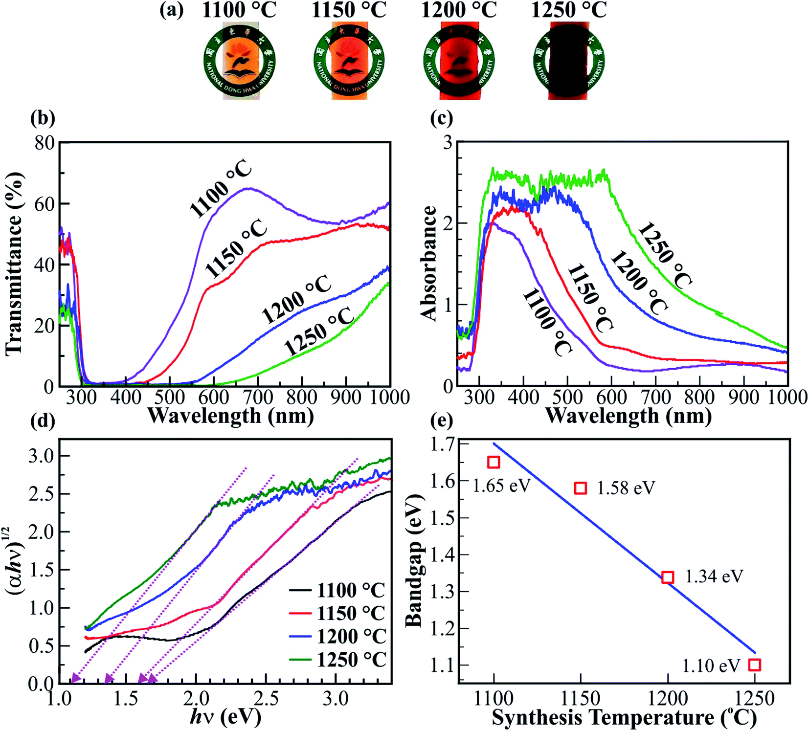 | ||
| Fig. 5 Bandgap properties. (a) Photographs of the Fe2O3 nanostructured films@1100, 1150, 1200, and 1250 °C on ITO/glass substrates. The color of the Fe2O3 nanostructured films changes from orange to deep red with the elevation of synthesis temperature. (b) The transmittance and (c) absorbance spectra of the Fe2O3 nanostructured films synthesized at various temperatures. (d) The linear graphs of (αhν)1/2vs. hν for determining the Eg of the Fe2O3 nanostructured films. (e) The graph shows the linear bandgap reduction of the Fe2O3 nanostructured films with the elevation of synthesis temperature. | ||
In order to further understand the reduction of bandgap in Fe2O3 nanostructured films, the valence band (VB) is also investigated. Fig. 6a shows the VB XPS spectra of the Fe2O3 film-nanofibers. The VB edge is defined as the intersection of the two dashed lines.11 The binding energies of the VB edge for Fe2O3 nanostructured films@1100, 1150, 1200, and 1250 °C are located at 1.84, 1.60, 1.45, and 1.28 eV, respectively. Obviously, the binding energy of the VB edge reduces linearly with the elevated synthesis temperature, as shown in Fig. 6b. This means that the VBs of the Fe2O3 nanostructured films are lifted at the elevated synthesis temperature. The VB edge lift of 0.56 eV is completely matched with the reduction of bandgap in the Fe2O3 nanostructured films, as mentioned above. The highest levels of the VB are lifted, while the lowest levels of the CB are unchanged. As a result, the bandgap of Fe2O3 nanostructured films reduces with the elevated synthesis temperatures, as shown in the schematic illustration in Fig. 6c. The bandgap characteristics of the Fe2O3 nanostructured films are consistent with the second type of bandgap tuning, as shown in Fig. 1b. The reduction in the bandgap of Fe2O3 nanostructured films is only due to the gain in the Fe2+ cations and the cubic (γ) phase composition. This suggests that the bandgap (Eg) of the Fe2O3 nanostructured films can be tuned by controlling only the synthesis temperature. The characteristics of bandgap tuning without any doping make the Fe2O3 nanostructured films promising candidates for applications in bandgap engineering, optoelectronic devices, and energy storage devices.
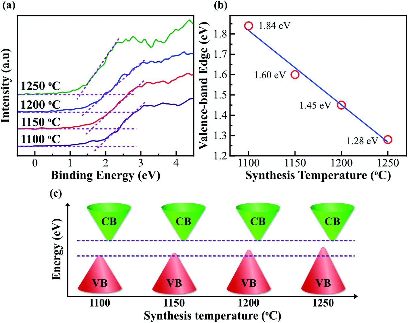 | ||
| Fig. 6 Valence-band-edge lifting. (a) The high-resolution valence-band (VB) XPS spectra of the Fe2O3 nanostructured films@1100, 1150, 1200, and 1250 °C. The binding energies of the VB edges are defined at the intersections of the dashed lines. (b) The graph shows the linear reduction of the VB edge with the elevation of synthesis temperature, indicating that the VB edge is lifted at high synthesis temperatures. (c) A schematic diagram shows the bandgap reduction of the Fe2O3 nanostructured films with the elevation of synthesis temperature. The characteristics of the bandgap reduction in the Fe2O3 nanostructured films are consistent with the second type of bandgap tuning, as shown in Fig. 1b. | ||
The electrochemical charge storage properties of Fe2O3 nanostructured films@1100, 1150, 1200, and 1250 °C are studied via cyclic voltammetry (CV) and electrochemical impedance spectroscopy (EIS) in 1 M KOH electrolyte. The CV and EIS results are shown in Fig. S12 (ESI†). The 1D nanorods produced at 1100 °C show the lowest specific capacitance value of ∼82 F g−1 at a scan rate of 50 mV s−1, while those produced at 1250 °C show the highest specific capacitance of ∼352 F g−1 at a low scan rate of 5 mV s−1. These specific capacitance values are higher than those of Fe2O3 thin film,33 Fe2O3 nanorods,33,57 Fe2O3 nanosheets,57 Fe2O3 nanoparticles,57 and nanoporous Fe2O3/CNT.58 This result makes Fe2O3 film nanofibers a potential supercapacitor electrode material candidate.
Conclusion
In this study, Fe3O4 and metallic Fe nanostructures were synthesized on ITO/glass substrates using the HFMOVD technique at temperatures of 1100, 1150, 1200, and 1250 °C. The Fe3O4 and metallic Fe nanostructures were then fully oxidized using the thermal oxidation technique, yielding Fe2O3 nanostructured films at 500 °C for 4 hours in a ∼500 Torr O2 atmosphere. The formation of nanosheets and nanofibers can be attributed to the presence of metallic iron in the samples that were synthesized at temperatures of 1150, 1200, and 1250 °C. The Fe2O3 nanostructured films comprise two combinations of the trigonal (α) and cubic (γ) phases, and two mixtures of the Fe2+ and Fe3+ cations. The crystal composition of the cubic (γ) phase and the amount of the Fe2+ cations increase linearly from 0 to ∼23.7% and ∼6.11 to ∼13.5% with the elevated synthesis temperature, respectively, implying that the valence band will gain more electrons and be lifted at higher synthesis temperatures. Therefore, the phase combination and cation mixture play a critical role in tuning the bandgap of the Fe2O3 nanostructured films. The linear bandgap reduction of 0.55 eV is only controlled by the synthesis temperature without any doping, indicating the potential of the Fe2O3 nanostructured films for applications in bandgap engineering, optoelectronic devices, and energy storage devices.Author contributions
Sujit A. Kadam: conceptualization, methodology, validation, investigation, data curation, writing – original draft. Giang Thi Phan: formal analysis, investigation, methodology, validation, writing – original draft. Duy Van Pham: data curation, methodology, validation, formal analysis, investigation, visualization, funding acquisition, writing – original draft, writing – review & editing. Ranjit A Patil: investigation, resources. Chien-Chih Lai: resources, software, funding acquisition. Yan-Ruei Chen: investigation. Yung Liou: investigation, resources. Yuan-Ron Ma: investigation, resources, validation, writing – review & editing, project administration, funding acquisition, supervision.Conflicts of interest
There are no conflicts to declare.Acknowledgements
The authors would like to thank the Ministry of Science and Technology (MOST), Taiwan for their financial support of this research under Contract No. MOST 108-2112-M-259-007-MY3, MOST 109-2112-M-259-008, and MOST 110-2811-M-002-651.References
- K. Gao, Y. Kan, X. Chen, F. Liu, B. Kan, L. Nian, X. Wan, Y. Chen, X. Peng, T. P. Russell, Y. Cao and A. K. Y. Jen, Adv. Mater., 2020, 32, 1906129 CrossRef CAS.
- R. Prasanna, A. Gold-Parker, T. Leijtens, B. Conings, A. Babayigit, H.-G. Boyen, M. F. Toney and M. D. McGehee, J. Am. Chem. Soc., 2017, 139, 11117–11124 CrossRef CAS.
- T. Todorov, T. Gershon, O. Gunawan, Y. S. Lee, C. Sturdevant, L.-Y. Chang and S. Guha, Adv. Energy Mater., 2015, 5, 1500799 CrossRef.
- S.-W. Wang, H. Medina, K.-B. Hong, C.-C. Wu, Y. Qu, A. Manikandan, T.-Y. Su, P.-T. Lee, Z.-Q. Huang, Z. Wang, F.-C. Chuang, H.-C. Kuo and Y.-L. Chueh, ACS Nano, 2017, 11, 8768–8776 CrossRef CAS PubMed.
- S. Wang, Y. Guo, D. Feng, L. Chen, Y. Fang, H. Shen and Z. Du, J. Mater. Chem. C, 2017, 5, 4724–4730 RSC.
- S. Engmann, A. J. Barito, E. G. Bittle, N. C. Giebink, L. J. Richter and D. J. Gundlach, Nat. Commun., 2019, 10, 227 CrossRef PubMed.
- Y. Kim, H. Bark, B. Kang and C. Lee, ACS Appl. Mater. Interfaces, 2019, 11, 12613–12621 CrossRef CAS.
- B. Li, T. Xing, M. Zhong, L. Huang, N. Lei, J. Zhang, J. Li and Z. Wei, Nat. Commun., 2017, 8, 1958 CrossRef.
- S. Feng, Z. Lin, X. Gan, R. Lv and M. Terrones, Nanoscale Horiz., 2017, 2, 72–80 RSC.
- G. M. Lohar, S. T. Jadhav, M. V. Takale, R. A. Patil, Y. R. Ma, M. C. Rath and V. J. Fulari, J. Colloid Interface Sci., 2015, 458, 136–146 CrossRef CAS PubMed.
- G. T. Phan, D. V. Pham, R. A. Patil, C.-C. Lai, W.-C. Yeh, Y. Liou and Y.-R. Ma, Applied Materials Today, 2019, 15, 605–613 CrossRef.
- Y. Lu and J. Guo, Nano Res., 2010, 3, 189–199 CrossRef CAS.
- Y. Li, T. Wang, M. Wu, T. Cao, Y. Chen, R. Sankar, R. K. Ulaganathan, F. Chou, C. Wetzel, C.-Y. Xu, S. G. Louie and S.-F. Shi, 2D Mater., 2018, 5, 021002 CrossRef.
- B. Deng, V. Tran, Y. Xie, H. Jiang, C. Li, Q. Guo, X. Wang, H. Tian, S. J. Koester, H. Wang, J. J. Cha, Q. Xia, L. Yang and F. Xia, Nat. Commun., 2017, 8, 14474 CrossRef CAS PubMed.
- Y. L. Huang, Y. Chen, W. Zhang, S. Y. Quek, C.-H. Chen, L.-J. Li, W.-T. Hsu, W.-H. Chang, Y. J. Zheng, W. Chen and A. T. S. Wee, Nat. Commun., 2015, 6, 6298 CrossRef PubMed.
- D. V. Pham, R. A. Patil, J.-H. Lin, C.-C. Lai, Y. Liou and Y.-R. Ma, Nanoscale, 2016, 8, 5559–5566 RSC.
- B. S. Chang, A. Martin, B. Thomas, A. Li, R. W. Dorn, J. Gong, A. J. Rossini and M. M. Thuo, ACS Mater. Lett., 2020, 2, 1211–1217 CrossRef CAS.
- W. S. Choi, M. F. Chisholm, D. J. Singh, T. Choi, G. E. Jellison and H. N. Lee, Nat. Commun., 2012, 3, 689 CrossRef.
- H. Zeuthen, W. Kudernatsch, L. R. Merte, L. K. Ono, L. Lammich, F. Besenbacher and S. Wendt, ACS Nano, 2015, 9, 573–583 CrossRef CAS.
- R. Paul, R. G. Reifenberger, T. S. Fisher and D. Y. Zemlyanov, Chem. Mater., 2015, 27, 5915–5924 CrossRef CAS.
- J. Muro-Cruces, A. G. Roca, A. López-Ortega, E. Fantechi, D. del-Pozo-Bueno, S. Estradé, F. Peiró, B. Sepúlveda, F. Pineider, C. Sangregorio and J. Nogues, ACS Nano, 2019, 13, 7716–7728 CrossRef CAS PubMed.
- J. Zhao, Y. Niu, B. Ren, H. Chen, S. Zhang, J. Jin and Y. Zhang, Chem. Eng. J., 2018, 347, 574–584 CrossRef CAS.
- R. Sinmyo, E. Bykova, S. V. Ovsyannikov, C. McCammon, I. Kupenko, L. Ismailova and L. Dubrovinsky, Sci. Rep., 2016, 6, 32852 CrossRef CAS.
- A. G. Tamirat, J. Rick, A. A. Dubale, W.-N. Su and B.-J. Hwang, Nanoscale Horiz., 2016, 1, 243–267 RSC.
- Y. Makimizu, J. Yoo, M. Poornajar, N. T. Nguyen, H.-J. Ahn, I. Hwang, S. Kment and P. Schmuki, J. Mater. Chem. A, 2020, 8, 1315–1325 RSC.
- J. D. Emery, C. M. Schlepütz, P. Guo, S. C. Riha, R. P. H. Chang and A. B. F. Martinson, ACS Appl. Mater. Interfaces, 2014, 6, 21894–21900 CrossRef CAS.
- Y. Zhang, N. Zhang, T. Wang, H. Huang, Y. Chen, Z. Li and Z. Zou, Appl. Catal., B, 2019, 245, 410–419 CrossRef CAS.
- K. Liang, L. S. Hui and A. Turak, Nanoscale, 2019, 11, 9076–9084 RSC.
- J. Huang, M. Guo, H. Ke, C. Zong, B. Ren, G. Liu, H. Shen, Y. Ma, X. Wang, H. Zhang, Z. Deng, H. Chen and Z. Zhang, Adv. Mater., 2015, 27, 5049–5056 CrossRef CAS PubMed.
- G. Segev, H. Dotan, K. D. Malviya, A. Kay, M. T. Mayer, M. Grätzel and A. Rothschild, Adv. Energy Mater., 2016, 6, 1500817 CrossRef.
- L.-L. Tian, M.-J. Zhang, C. Wu, Y. Wei, J.-X. Zheng, L.-P. Lin, J. Lu, K. Amine, Q.-C. Zhuang and F. Pan, ACS Appl. Mater. Interfaces, 2015, 7, 26284–26290 CrossRef CAS PubMed.
- J. Zhao, Z. Li, X. Yuan, Z. Yang, M. Zhang, A. Meng and Q. Li, Adv. Energy Mater., 2018, 8, 1702787 CrossRef.
- Y. Li, J. Xu, T. Feng, Q. Yao, J. Xie and H. Xia, Adv. Funct. Mater., 2017, 27, 1606728 CrossRef.
- T. Jiang, F. Bu, X. Feng, I. Shakir, G. Hao and Y. Xu, ACS Nano, 2017, 11, 5140–5147 CrossRef CAS.
- X. Zhu, Y. Zhu, S. Murali, M. D. Stoller and R. S. Ruoff, ACS Nano, 2011, 5, 3333–3338 CrossRef CAS PubMed.
- K. Cao, L. Jiao, H. Liu, Y. Liu, Y. Wang, Z. Guo and H. Yuan, Adv. Energy Mater., 2015, 5, 1401421 CrossRef.
- J. C. Espinosa, C. Catalá, S. Navalón, B. Ferrer, M. Álvaro and H. García, Appl. Catal., B, 2018, 226, 242–251 CrossRef CAS.
- S. H. Yoo, D. Jang, H.-I. Joh and S. Lee, J. Mater. Chem. A, 2017, 5, 748–755 RSC.
- K. Zhao, H. Tang, B. Qiao, L. Li and J. Wang, ACS Catal., 2015, 5, 3528–3539 CrossRef CAS.
- C. Yin, C. Gong, J. Chu, X. Wang, C. Yan, S. Qian, Y. Wang, G. Rao, H. Wang, Y. Liu, X. Wang, J. Wang, W. Hu, C. Li and J. Xiong, Adv. Mater., 2020, 32, 2002237 CrossRef CAS PubMed.
- L. Wan, H. Song, J. Ma, Y. Ren, X. Cheng, J. Su, Q. Yue and Y. Deng, ACS Appl. Mater. Interfaces, 2018, 10, 13028–13039 CrossRef CAS PubMed.
- Z.-F. Dou, C.-Y. Cao, Q. Wang, J. Qu, Y. Yu and W.-G. Song, ACS Appl. Mater. Interfaces, 2012, 4, 5698–5703 CrossRef CAS PubMed.
- W. Geng, S. Ge, X. He, S. Zhang, J. Gu, X. Lai, H. Wang and Q. Zhang, ACS Appl. Mater. Interfaces, 2018, 10, 13702–13711 CrossRef CAS.
- D. V. Pham, R. A. Patil, C.-C. Yang, W.-C. Yeh, Y. Liou and Y.-R. Ma, Nano Energy, 2018, 47, 105–114 CrossRef CAS.
- R. A. Patil, R. S. Devan, J.-H. Lin, Y.-R. Ma, P. S. Patil and Y. Liou, Sol. Energy Mater. Sol. Cells, 2013, 112, 91–96 CrossRef CAS.
- J.-H. Lin, R. A. Patil, M.-A. Wu, L.-G. Yu, K.-D. Liu, W.-T. Gao, R. S. Devan, C.-H. Ho, Y. Liou and Y.-R. Ma, J. Mater. Chem. C, 2014, 2, 8667–8672 RSC.
- R. S. Devan, Y.-R. Ma, M. A. More, R. T. Khare, V. V. Antad, R. A. Patil, V. P. Thakare, R. S. Dhayal and L. Schmidt-Mende, RSC Adv., 2016, 6, 98722–98729 RSC.
- G. T. Phan, D. V. Pham, R. A. Patil, C.-H. Tsai, C.-C. Lai, W.-C. Yeh, Y. Liou and Y.-R. Ma, Sol. Energy Mater. Sol. Cells, 2021, 231, 111306 CrossRef CAS.
- W. Zhang, Y. Wu, J. Qi, M. Chen and R. Cao, Adv. Energy Mater., 2017, 7, 1602547 CrossRef.
- Y. Wu, M. Chen, Y. Han, H. Luo, X. Su, M.-T. Zhang, X. Lin, J. Sun, L. Wang, L. Deng, W. Zhang and R. Cao, Angew. Chem., Int. Ed., 2015, 54, 4870–4875 CrossRef CAS PubMed.
- H. Wang, F. Yin, B. Chen and G. Li, J. Mater. Chem. A, 2015, 3, 16168–16176 RSC.
- T. Wang, B. Daiber, J. M. Frost, S. A. Mann, E. C. Garnett, A. Walsh and B. Ehrler, Energy Environ. Sci., 2017, 10, 509–515 RSC.
- A. Loiudice, J. Ma, W. S. Drisdell, T. M. Mattox, J. K. Cooper, T. Thao, C. Giannini, J. Yano, L. W. Wang, I. D. Sharp and R. Buonsanti, Adv. Mater., 2015, 27, 6733–6740 CrossRef CAS.
- M. Bernechea, Y. Cao and G. Konstantatos, J. Mater. Chem. A, 2015, 3, 20642–20648 RSC.
- X. Xie, C. Mao, X. Liu, L. Tan, Z. Cui, X. Yang, S. Zhu, Z. Li, X. Yuan, Y. Zheng, K. W. K. Yeung, P. K. Chu and S. Wu, ACS Cent. Sci., 2018, 4, 724–738 CrossRef CAS.
- W. Dong, H. Liu, J. K. Behera, L. Lu, R. J. H. Ng, K. V. Sreekanth, X. Zhou, J. K. W. Yang and R. E. Simpson, Adv. Funct. Mater., 2018, 29, 1806181 CrossRef.
- Y. Li, Q. Li, L. Cao, X. Cui, Y. Yang, P. Xiao and Y. Zhang, Electrochim. Acta, 2015, 178, 171–178 CrossRef CAS.
- C.-H. Xu, P.-Y. Shen, Y.-F. Chiu, P.-W. Yeh, C.-C. Chen, L.-C. Chen, C.-C. Hsu, I. C. Cheng and J.-Z. Chen, J. Alloys Compd., 2016, 676, 469–473 CrossRef CAS.
Footnote |
| † Electronic supplementary information (ESI) available: Top- and side-view FESEM images of the nanostructured films before and after annealing, XRD patterns before annealing, XRD Rietveld analysis of the Fe2O3 nanostructured films, TEM analysis of the Fe2O3 thin film@1100 °C, etc. See DOI: 10.1039/d1na00442e |
| This journal is © The Royal Society of Chemistry 2021 |