
 Open Access Article
 This Open Access Article is licensed under a Creative Commons Attribution-Non Commercial 3.0 Unported Licence
Correlation analysis of vibration modes in physical vapour deposited Bi2Se3 thin films probed by the Raman mapping technique†
K. A.
Niherysh
ab,
J.
Andzane
a,
M. M.
Mikhalik
b,
S. M.
Zavadsky
b,
P. L.
Dobrokhotov
c,
F.
Lombardi
 d,
S. L.
Prischepa
bc,
I. V.
Komissarov
*bc and
D.
Erts
*ae
d,
S. L.
Prischepa
bc,
I. V.
Komissarov
*bc and
D.
Erts
*ae
aInstitute of Chemical Physics, University of Latvia, Riga, Latvia. E-mail: donats.erts@lu.lv
bBelarusian State University of Informatics and Radioelectronics, Minsk, Belarus. E-mail: komissarov@bsuir.by
cNational Research Nuclear University MEPhI (Moscow Engineering Physics Institute), Moscow, Russia
dQuantum Device Physics Laboratory, Department of Microtechnology and Nanoscience, Chalmers University of Technology, Gothenburg, Sweden
eFaculty of Chemistry, University of Latvia, Riga, Latvia
First published on 8th October 2021
Abstract
In this work, the Raman spectroscopy mapping technique is used for the analysis of mechanical strain in Bi2Se3 thin films of various (3–400 nm) thicknesses synthesized by physical vapour deposition on amorphous quartz and single-layer graphene substrates. The evaluation of strain effects is based on the correlation analysis of in-plane (E2g) and out-of-plane (A21g) Raman mode positions. For Bi2Se3 films deposited on quartz, experimental datapoints are scattered along the line with a slope  of ∼0.85, related to the distribution of hydrostatic strain. In contrast to quartz/Bi2Se3 samples, for graphene/Bi2Se3 heterostructures with the same thicknesses, an additional negative slope of ∼−0.85, which can be associated with the distribution of the in-plane (a–b) biaxial tensile strain due to the film–substrate lattice mismatch, is observed. The algorithm of phonon deformation potential (PDP) calculation based on the proposed strain analysis for the 3 nm thick Bi2Se3 film deposited on the graphene substrate, where the strain is considered to be coherent across the thickness, is demonstrated. The PDPs for biaxial in-plane strain of the Bi2Se3 3 nm film in in-plane and out-of-plane modes are equal to −7.64 cm−1/% and −6.97 cm−1/%, respectively.
Introduction
Linear energy–momentum dispersion in graphene and topological insulators (TIs) has made these materials as well as van der Waals heterostructures based on them the focus of scientific interest for the last decade. Various devices for electronic, spintronic and even domestic waste heat conversion applications can be realised based on graphene/TI heterostructures.1–6 Although the physical properties of these 2D materials are rather well understood, their wide practical applications are still challenging due to the extreme sensitivity of these materials to the substrates they are supported by. Strain is one of the most prominent phenomena occurring at the interface of the contacting materials which can change their band structure.7–10 Therefore, strain can be considered not only as a problem that must be taken into account when designing a device, but also as an opportunity to tune the properties of the material. In the case of topological insulators, theoretical studies indicate that the bulk band gap and the spin-polarized Dirac surface states can be tailored by strain.11,12 It was experimentally demonstrated that compressive strain in the out-of-plane direction reduces the bandgap of the surface state of Bi2Se3 films on epi-graphene on SiC.5 Previously, it was also theoretically indicated that variations in the concentration of charge carriers caused by doping and the presence of mechanical strain in TIs can affect the thermoelectric power of these materials.13Strain, defined as the lattice parameter deviation of a material from its bulk value quantitatively expressed as ε = (a − a0)/a0, where a is the lattice parameter of the strained material and a0 is the value of the bulk, is most commonly caused by the lattice mismatch between the deposited material and the substrate.14,15 However, as the growth of materials is usually performed at elevated temperatures, the difference in the thermal expansion coefficients (TECs) of the deposited material and the substrate is also a source of strain.16 Separation of the impact and control of strain sources are required for precise engineering of the physical properties of TI materials.
Besides the measurement techniques commonly applied for the ex situ and in situ structural characterization of 3D materials such as X-ray diffraction (XRD) or reflection high-energy electron diffraction (RHEED), micro-Raman spectroscopy is considered as a powerful and non-destructive tool for the determination of mechanical strain in materials with micrometric spatial resolution.17 The micro-Raman spectroscopy technique is especially useful for the structural characterization of graphene and ultrathin films deposited by PVD as it is not subject to the technical limitations typical of the XRD and RHEED methods.18,19 For example, in the case of graphene the correlation analysis of G and 2D Raman mode positions can be used not only to separate the impact of strain and charge carrier density on the phonon spectrum, but also to calculate the absolute values of these parameters.20–23 This fact makes the correlation analysis of Raman modes a unique tool for studying the properties of materials.
In Raman spectroscopy, the phonon deformation potential (PDP) is the quantity connecting strain and Raman shift. It strongly depends on the thickness of the material, and sophisticated experiments have been performed to extract this dependency for bismuth chalcogenides.24,25 In these studies strain was introduced via either artificial24 or natural bending25 in the transferred film and nanoribbons, respectively; the Raman shift coefficients were evaluated for thickness in the range of 79–260 nm, limiting their applicability to the case of epitaxial ultrathin films. The theoretically estimated value of PDP for a 2 nm thin chalcogenide film is expected to be ∼5 cm−1/%.10
In this work, a systematic study of mechanical strain in single-layer graphene/Bi2Se3 (SLG/Bi2Se3) heterostructures with different Bi2Se3 layer thicknesses, and in Bi2Se3 films of the same thicknesses deposited on quartz substrates (Q/Bi2Se3) is performed. The methodological approach based on the correlation analysis of the experimental Raman data was applied to evaluate the nature of strain in the deposited films. To the best of our knowledge, such a kind of correlation analysis for topological insulator ultrathin films has been performed for the first time. In addition, an original method is proposed for estimating the phonon deformation potential in Bi2Se3 ultrathin films based on the correlation analysis approach presented in this work.
Methods
Bi2Se3 films of various thicknesses (3–400 nm) were synthesized by the physical vapour deposition technique (PVD)4,6,26,27 using a single-zone quartz tube furnace (GCL-1100X, MTI Corp.). SLG was synthesized using a First Nano Easy tube 101 CVD reactor and transferred from copper foil (GoodFellow) onto quartz (fused silica) slides (Agar scientific) by the methyl methacrylate (PMMA) polymer-assisted method.28 Based on the results of the structural analysis of graphene performed by the reflection high energy electron diffraction (RHEED) technique and the results of the structural analysis of copper foil performed by X-ray diffraction (XRD) we conclude that the graphene synthesized in our work can be described as a set of differently oriented domains with limited azimuthal angle distribution (see ESI S1†). These graphene as well as quartz samples were used as substrates for Bi2Se3 film deposition.The structure, morphology and stoichiometry of the deposited Bi2Se3 films were inspected using a field emission scanning electron microscope (FESEM), Hitachi S-4800, equipped with a Bruker XFlash Detector 5010 for energy dispersive X-ray spectrometry (EDS).
Thicknesses of SLG/Bi2Se3 heterostructures and Q/Bi2Se3 samples were measured using an atomic force microscope (AFM), Asylum Research MFP-3D. To measure the thickness of the films an artificial scratch was introduced. The mechanical hardness of the tool for creating a scratch exceeds the hardness of Bi2Se3, but is softer than quartz, which excludes deformation of the substrate.
XRD patterns of SLG/Bi2Se3 were obtained using CuKα radiation with an Ultima IV (Rigaku) diffractometer (λ = 0.15406 nm). XRD patterns of the copper foil were obtained using CuKα radiation with a DRON-3 diffractometer (λ = 0.15406 nm).
RHEED patterns of graphene were recorded in a custom-made (Chalmers University of Technology) pulsed laser deposition system, the base pressure is 2 × 10⁻⁷ mbar and the electron energy is 30 keV.
Raman spectra of SLG (see ESI S2†), SLG/Bi2Se3 and Q/Bi2Se3 structures were obtained at room temperature using a scanning laser confocal micro-Raman spectrometer, Confotec NR 500, by scanning sample areas of 20 × 20 μm2 with 785 nm (for Bi2Se3 films) and 473 nm (for graphene) excitation wavelengths and 100× objective. The accumulation time of the signal for each spectrum was 10 seconds. The laser beam diameter was about 600 nm. Raman spectra were recorded using 1800 l mm−1 and 1200 l mm−1 gratings, and spectral resolution of ∼0.2 cm−1 and ∼1 cm−1 for Bi2Se3 thin films and graphene, respectively. Throughout these measurements the edge filter cutting at ∼85 cm−1 was used.
Results
Bi2Se3 thin films with thicknesses 3–400 nm deposited on SLG and on quartz substrates were found to have uniform distribution of Bi and Se chemical elements over the area of ∼100 × 100 mm2 at a chemical composition of 40 at% for Bi and 60 at% for Se, which corresponds to a stoichiometry of Bi2Se3. Fig. 1a illustrates an example of the EDS spectrum and SEM image of the 11 nm thick Bi2Se3 film deposited on SLG. The XRD spectrum analysis of the SLG/Bi2Se3 structures revealed the presence of diffraction peaks related only to the (0 0 3n) family group, thus confirming the epitaxial growth of the Bi2Se3 thin film with the crystallographic c-axis oriented perpendicularly to the substrate surface.4,29 The XRD spectrum of the SLG/Bi2Se3 heterostructure with Bi2Se3 thickness of 11 nm and the pole figure taken from the diffraction maximum (0 0 6) are shown in Fig. 1b. The pole figure was recorded in a sweep from 0 to 70 degrees. The presence of only one (central) broad maximum on the pole figure means that the crystals of Bi2Se3 are coherently oriented in the c-direction, revealing good quality of epitaxial growth. All Bi2Se3 films were continuous with the relatively smooth surface. The representative AFM images and height profiles of Bi2Se3 (11 nm) film deposited on quartz and graphene are shown in Fig. 1c and d, respectively. AFM images of all samples as well as values of root mean square (RMS) roughness are presented in ESI S3.† | ||
| Fig. 1 (a) Energy-dispersive spectroscopy (EDS) spectrum of Bi2Se3 film (11 nm); inset – scanning electron microscopy (SEM) image of Bi2Se3 (11 nm) film deposited on SLG; (b) 2θ X-ray diffraction pattern of Bi2Se3 thin film (11 nm) deposited on SLG; inset – pole figure along the (0 0 6) plane; (c) atomic force microscopy (AFM) image of Bi2Se3 (11 nm) film on quartz and (d) on graphene with artificial scratches introduced to determine the thickness; insets – the height profiles of these films. | ||
A typical Raman spectrum of the SLG/Bi2Se3 (3 nm) in the range of 85 to 350 cm−1 for Bi2Se3 and of 650 to 3000 cm−1 for SLG is presented in Fig. 2a. It should be noted that the D band intensity of graphene, which is responsible for defects, is at the noise level before deposition of Bi2Se3 films (ESI S2†). And there is an appearance of insignificant peak D (still close to the noise level) after the deposition of Bi2Se3 films (ESI S4†). Two characteristic peaks at ∼131 cm−1 and ∼174 cm−1 respectively correspond to the in-plane (E2g) and out-of-plane (A21g) vibrational modes of the rhombohedral crystal structure of Bi2Se3 (Fig. 2a, inset).30 Raman E2g and A21g band mappings performed for SLG/Bi2Se3 and Q/Bi2Se3 samples with Bi2Se3 layer thicknesses of 3–400 nm showed Bi2Se3 peaks (without distortion and additional peaks) at each mapping point, which are well fitted by Lorentzian functions. This fact is consistent with the XRD data and confirms the uniformity, continuity and high quality of homogeneous ultrathin Bi2Se3 films grown on graphene and quartz substrates. The representative Raman mappings for the SLG/Bi2Se3 heterostructure with a 3 nm thin Bi2Se3 layer are shown in Fig. 2b and c.
 | ||
| Fig. 2 (a) Raman spectrum of graphene and 3 nm Bi2Se3 film synthesized on it; inset – the displacement patterns of phonon modes in the Bi2Se3 structure; (b and c) Raman mapping images of the 3 nm Bi2Se3 film with the corresponding histograms (insets): (b) E2g band position; (c) A21g band position; the colour scales represent the amplitude of measured values. | ||
Discussion
To perform the correlation analysis of Bi2Se3 films deposited on quartz (Fig. 3a) and graphene (Fig. 3b) the experimental Raman datapoints of Bi2Se3 were plotted in the coordinates of a higher frequency mode vs. lower frequency mode (A21gvs. E2g).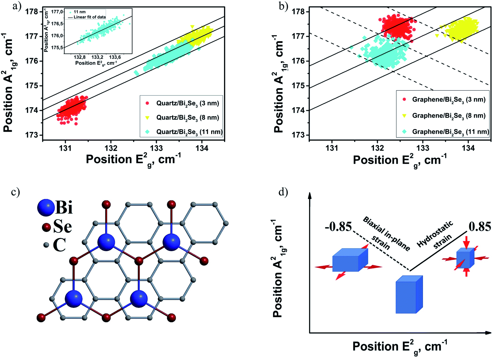 | ||
| Fig. 3 The positions of the A21g band as a function of E2g band positions for Bi2Se3 ultrathin films deposited on quartz (a) and graphene (b); the inset in Fig. 3a is a linear fit of A21gvs. E2g dependency for 11 nm Bi2Se3; (c) top view of the SLG/Bi2Se3 interlayer stacking pattern. (d) Bi2Se3 strain distribution scheme based on the A21g band as a function of E2g Raman band positions scattered along different slopes. The solid line with the slope of 0.85 corresponds to the hydrostatic strain of Bi2Se3. The dashed line with the slope of −0.85 corresponds to the biaxial in-plane tensile strain of Bi2Se3 (see the text for more details). | ||
Fig. 3a indicates the pronounced scattering of data points (A21g on E2g positions) of the Bi2Se3 ultrathin films deposited on quartz along the straight lines with the slope of ∼0.85 (this value was obtained from a linear fitting of datapoints for Bi2Se3 films deposited on quartz, Fig. 3a, inset). The deviation of experimental data from their linear fit is less than 0.5 cm−1, which is comparable with the spectral resolution of the Raman measurements and reveals strong reliability of the claimed dependency. The Raman frequency vibrations in topological insulators such as Bi2Se3 are governed by various thickness-dependent factors, including spin orbit coupling,31 charge carrier concentration,32 and strain.24 The linear scattering of A21g on E2g experimental points is most probably related to the distribution of strain value in the films. Indeed, for the experimental values of Raman hydrostatic pressure coefficients  and
and  ,33,34 their ratio is
 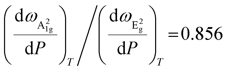 , which is in good agreement with the experimental data presented above. The scatter of the experimental datapoints along solid lines with a slope of ∼0.85 (Fig. 3a) indicates that Bi2Se3 films deposited on quartz experience strain distributed hydrostatically throughout the film (i.e. crystal lattices are strained or expanded both in-plane and out-of-plane simultaneously as illustrated in Fig. 3d). Presumably, this distribution of the strain may be related to the growth process specifics such as different TECs of the quartz substrate (∼0.5 × 10⁻⁶ K−1 (ref. 35)) and PVD-grown Bi2Se3 (∼11–19 × 10−6 K−1 (ref. 36)) and Volmer–Weber thin film growth mode, where growth occurs not layer-by-layer, but by the formation of separate islands, which subsequently coalesce.6,26,29 Indeed, the Volmer–Weber growth mechanism of Bi2Se3 films leads to the appearance of strain which is mainly concentrated in the grooves between the grains. In the case of strong interaction of the deposited material with the substrate, this type of strain is considered to be hydrostatic.37
In contrast to the scatter of the A21gvs. E2g datapoints of Q/Bi2Se3 samples, the scatter of the datapoints for Bi2Se3 thin films deposited on SLG does not show a pronounced linear shape (Fig. 3b), but rather rhomb-shaped spots with additional scatter of experimental datapoints along the dashed line with a negative slope (∼−0.85) are observed. This could be explained by the red-shift of the in-plane E2g Raman mode positions and simultaneous blue-shift of the out-of-plane A21g mode positions, which are related to the in-plane tensile strain, originating from the lattice mismatch between the SLG and Bi2Se3. Assuming the same absolute values of Raman pressure coefficients for both compressive and tensile strains, in the case of biaxial strain a scatter of the experimental datapoints along the line with the slope ∼−0.85 should be obtained, in contrast with the hydrostatic strain (Fig. 3a). As the hexagonal lattice constant of the SLG is smaller than the Bi2Se3 lattice constant (Fig. 3c), the Bi2Se3 epitaxial film should experience in-plane tensile strain and compressive strain parallel to the c-axis.1 Indeed, due to the hexagonal honeycomb lattice of graphene (the lattice constant aGr = 2.46 Å), the stacking pattern between single layer graphene and Bi2Se3 with surface Se atoms in the hollow centres of carbon hexahedral rings (Fig. 3c) has the lowest binding energy and thus is a stable structure.38 The relationship between Bi2Se3 and graphene lattice parameters is  . For this stacking order the lattice mismatch for Bi2Se3 (tensile strain) is 2.9%. The experimental value of lattice parameter c for 11 nm Bi2Se3 film deposited on graphene, extracted from the most intensive XRD peaks 006 (2θ006 = 18.584°) and 0015 (2θ0015 = 47.615°) (Fig. 1b), is equal to 28.624 Å, which is less than the lattice constant for the relaxed bulk value (28.636 Å).39 However, it is worth mentioning here that the obtained experimental value may differ from the real crystal lattice parameter. The accurate evaluation of lattice parameters in our case cannot be performed because amorphous quartz used as the supporting substrate for the graphene/TI heterostructure does not possess any XRD reflections which can be used for the precise positioning of the sample in the XRD goniometer.
Thus, the approach to the separation of the origin of strain in PVD-deposited ultrathin Bi2Se3 films on quartz and SLG substrates based on the correlation analysis of Raman mode behaviour is as follows (Fig. 3d): scatter of the experimental A21gvs. E2g datapoints along the solid line with a positive slope (∼0.85) is associated with simultaneous compression or extension both in-plane and along the c-axis (hydrostatic strain); in turn, scatter of these datapoints along the dashed line with a negative slope (∼−0.85) is associated with the biaxial in-plane strain caused by the lattice mismatch of the heterostructure layers.
It is important to note here that the scattering of experimental datapoints for thicker Bi2Se3 films synthesized on quartz and graphene substrates retained the claimed behaviour and is discussed in ESI S5.†
As was pointed out above, the Raman technique has the advantage of providing non-contact probing of physical properties and provides access for simultaneous measurements of materials in heterostructures. Therefore, the developed theory of Raman scattering in SLG allows calculation of the lattice parameter of graphene in the studied heterostructures based on the correlation analysis of 2D and G band positions.23 In turn, the Bi2Se3 in-plane lattice parameter can be calculated according to the atomic arrangement presented in Fig. 3c. Thus, the in-plane strain in Bi2Se3 film deposited on graphene can be evaluated. It is worth mentioning that this approach is applicable only to thin coherently strained films. Indeed, the crystal size calculation for 11 nm thick film from the 006 XRD reflection (ESI S6†) is in good agreement with AFM thickness measurements. Thus, the coherence condition is satisfied.
Fig. 4 shows the dependency of the 2D band on G band positions for graphene with Bi2Se3 ultrathin films of different thicknesses deposited on it.
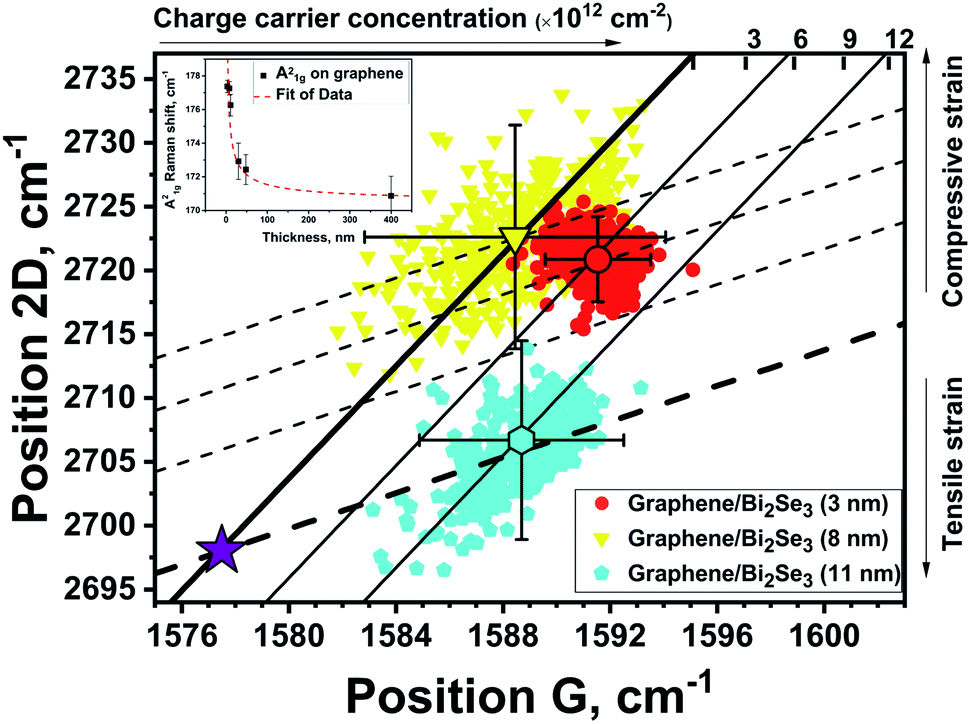 | ||
| Fig. 4 Position of the 2D band as a function of the G band position for graphene/Bi2Se3 heterostructures with different thicknesses of Bi2Se3 (listed in the inbox) deposited on graphene. The purple star mark is the position of unstrained and undoped graphene.23,40 The central large symbols of the same color as the marks of the samples represent the averaged value for 400 spectra recorded for each sample and its standard deviation in ΔG and Δ2D, respectively. The bold solid line (with a slope of ∼2.2) passing through the purple star mark is responsible for the biaxial strain in the ideal graphene. Solid lines (with a slope of ∼2.2) parallel to the bold solid line are responsible for the biaxial strain with fixed charge carrier concentrations. The bold dashed line (with a slope of ∼0.7) passing through the purple star mark is responsible for the charge carrier concentration in the ideal graphene. Dashed lines (with a slope of ∼0.7) parallel to the bold dashed line are responsible for the charge carrier concentration with fixed biaxial strain. | ||
It was previously shown that the position of the G band of graphene does not depend on the wavelength of the excitation laser,41 whereas the 2D band has dispersion dPos(2D)/dωL ∼ 100 cm−1 eV−1.42 Considering the nondispersive behaviour of the G band and using the dispersion together with the known position of the 2D band for the ideal unstrained and undoped graphene excited with 514 nm wavelength, ∼2677 cm−1,23,40 Raman shifts of G and 2D bands (the purple star mark (X = 1577.5 cm−1, Y = 2698 cm−1)) for the ideal graphene excited with 473 nm wavelength were obtained.
The Raman band shift related to the biaxial strain in the ideal graphene with a fixed charge carrier concentration is represented by the bold solid line (the slope of ∼2.2). In turn, the change of charge-carrier concentration at a fixed biaxial strain in ideal graphene is represented by a bold dashed line (the slope of ∼0.7).23
It is important to note that the strain and charge carrier concentration in CVD-grown graphene transferred on the surface of a solid substrate depend on transfer conditions and may vary from experiment to experiment, and even within the same sample.23,40 In accordance with the experimental Raman data (Fig. 4), SLG from the sample with 8 nm Bi2Se3 deposited on it is the most strained (yellow datapoints); then for the 3 nm thick film (red datapoints) graphene is slightly relaxed, whereas for the 11 nm thick film (cyan datapoints) graphene can be considered as completely unstrained. In compliance with the atomic arrangement presented in Fig. 3c, the in-plane strain in Bi2Se3 films behaves in the opposite manner (11 nm thick film on graphene is the most tensile strained, then 3 nm and, finally, 8 nm thick film).
The larger tensile in-plane strain should lead to the larger red-shift of the E2g Raman mode (in-plane vibrations). Indeed, that kind of a pattern is observed in the experimental data (Fig. 3b). In line with this logic, the 11 nm thick film on graphene should have the most blue-shifted A21g Raman mode (out-of-plane vibrations), but the experimental observation contradicts this prediction. This contradiction can be resolved by taking into account the thickness dependency of the A21g position, see the inset of Fig. 4. Indeed, such dependency is usually observed for Bi2Se3 films and explained by mechanisms other than strain such as charge transfer, spin–orbit coupling, confinement effect, and intersurface coupling.31,32 It means that these mechanisms have a much stronger influence upon the position of the A21g mode than the strain itself.
Even though the absolute value of the Raman shift cannot be directly linked to the strain in the films, the deviation of the strain can be calculated from the approach discussed above. In the framework of this approach, the distribution of the experimental data points along the negative slope in Fig. 3b should be associated with the distribution of graphene lattice parameter.
Using the proposed strain separation method (Fig. 3d), the PDP for the thinnest Bi2Se3 (3 nm) film deposited on graphene, where the film is fully strained by the substrate and strain is considered to be coherent across the thickness,1,31,43,44 can be calculated. This calculation is based on a simple idea. The in-plane tensile strain in 3 nm thin Bi2Se3 associated with the negative (∼−0.85) slope originates only from the lattice mismatch between the graphene and Bi2Se3. Therefore, the change in the Bi2Se3 lattice parameter is directly related to the change in the graphene lattice parameter (see Fig. 3c). Thus, the variation of the graphene lattice parameter can be easily transformed into variations of the Bi2Se3 plane lattice parameters. In combination with the variations of the A21g and E2g shifts, the PDP values of these modes for the Bi2Se3 in-plane strain can be obtained. The detailed step-by-step description of the PDP calculation is presented below.
For the strain range evaluation of the graphene layer in the SLG/Bi2Se3 heterostructure with the 3 nm thick Bi2Se3 layer such a Δω2D/ΔωG Raman data difference is plotted in Fig. 5a.
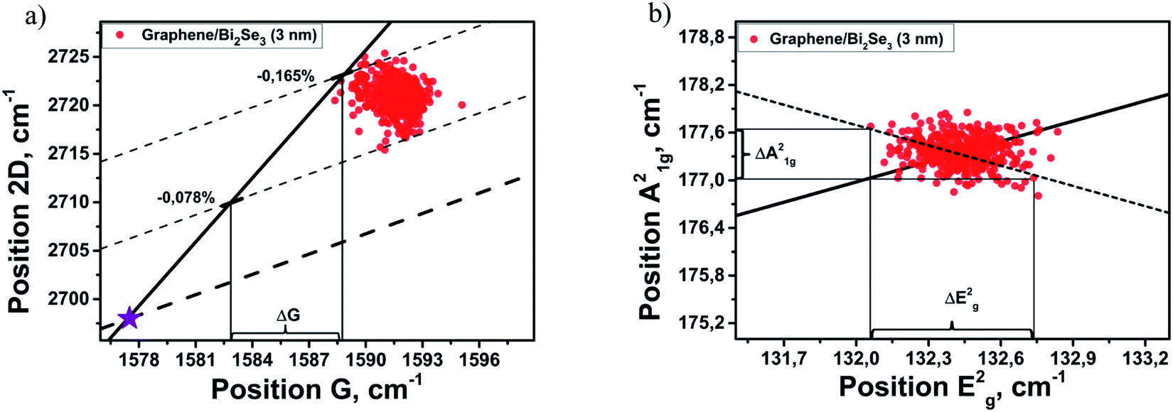 | ||
| Fig. 5 (a) 2D vs. G dependency of the graphene layer in the SLG/Bi2Se3 (3 nm) heterostructure. The purple star mark is the position of unstrained and undoped graphene.23,40 The bold solid line (slope ∼2.2) is related to the biaxial strain in the ideal graphene. Dashed lines (slope ∼0.7) are the change of charge-carrier concentration while biaxial strain is fixed; (b) A21gvs. E2g dependency for 3 nm Bi2Se3 film deposited on graphene. The solid line (slope ∼0.85) is related to the hydrostatic strain distribution. The dashed line (slope ∼−0.85) is related to the strain caused by graphene (lattice mismatch). | ||
Two dashed lines with a slope of ∼0.7 were drawn through the upper and lower points of the 2D vs. G plot to the intersection with the bold solid line (with a slope of ∼2.2) as shown in Fig. 5a. The strain range variation of the graphene layer can be calculated by determination of the difference ΔωG between the intersection points of the lines with a slope of ∼0.7 with the bold solid line, and the G band position for the ideal SLG (Fig. 5a, purple star mark), followed by dividing the calculated ΔωG values by the averaged sensitivity factor for the G band (−69.1 ± 3.4 cm−1/%23). Following the strain calculation procedure for the graphene layer in the SLG/Bi2Se3 heterostructures described above, the graphene strain range from −0.165% to −0.078% for the SLG/Bi2Se3 heterostructure with the 3 nm thin Bi2Se3 layer was determined. The lattice parameter of the strained graphene aGr3 nm was found to vary from 2.456 to 2.458 Å. Using these values, the lattice parameter for the Bi2Se3 layer in the SLG/Bi2Se3 heterostructure  was found to vary from 4.254 to 4.258 Å, which is equal to 2.80 to 2.89% tensile strain in the 3 nm thick Bi2Se3 film
  . The A21gvs. E2g plot for the 3 nm thick Bi2Se3 film deposited on SLG is shown in Fig. 5b. The dashed line with a slope of ∼−0.85 indicates the in-plane tensile strain introduced by Bi2Se3 and graphene lattice mismatch, and is associated with the blue and red shift of A21g and E2g modes respectively, which is consistent with other reports.1 Raman shifts corresponding to ΔE2g and ΔA21g estimated from Fig. 5b are equal to 0.68 cm−1 and 0.62 cm−1, respectively. This results in PDP values for biaxial in-plane strain for 3 nm thin Bi2Se3 film deposited on graphene of −7.64 cm−1/% for the in-plane mode and −6.97 cm−1/% for the out-of-plane mode.
Finally, let's compare our findings for PDP in Bi2Se3 with the literature results. In ref. 24 the A21g, E2g, and A11g modes are red-shifted with increase of applied strain and the Raman shift strain coefficient of the A21g mode is −1.68 cm−1/%, for the 79 nm thick film. A similar value for a 100 nm thick nanoribbon value has been reported in ref. 25 where the authors found the PDP (or the Raman shift strain coefficient) of A21g to be −1.78 cm−1/%. As mentioned by the authors of ref. 24 and 25 these values are already much larger than those reported for bulk materials,33 which implies strong inverse dependence of PDP on thickness.25 Therefore, our results for the 3 nm thick film correspond to this tendency. Moreover, we evaluated the Raman shift strain coefficient of A21g for the 2 nm Bi2Se3 thick film based on the estimated deformation given in ref. 24, which varies with the film thickness, ∼−4.83 cm−1/%. Considering the strong dependence of PDP (Raman shift strain coefficient) on the thickness together with 2 times difference in the out of plane strain for the same applied in-plane stress, εbiaxialzz = 2 × εuniaxialzz, (please see the ESI of ref. 24 and 45), we conclude a very good correlation of our results with those reported in the cited literature. It is worth mentioning that in both references considered, ref. 24 and 25, single spectra have been measured which may cause uncertainty in the measured value. In contrast, the proposed approach of strain separation using datapoint scatter along the straight lines with certain slopes is more statistically reliable than those presented previously24,25 since the tensile in-plane strain applied to the Bi2Se3 ultrathin film originates from the lattice mismatch between the film and graphene, as well as the calculation process uses all data recorded from a large area by the Raman mapping technique. The application of the proposed method of PDP calculation makes it possible to estimate this coefficient regardless of the deformation type (both under compression and tension) in the system (Fig. 3d).
Conclusion
The method of separation of two different origins of strain (hydrostatic and in-plane tensile caused by lattice mismatch) using Raman data analysis is developed and applied to Bi2Se3 films PVD-grown on quartz and CVD-graphene substrates. All samples were investigated using the Raman mapping technique over a 20 × 20 μm2 area. The correlation analysis of A21g and E2g position modes revealed that films grown on a quartz substrate experienced a hydrostatic strain distribution, which is evidenced by the location of A21gvs. E2g points along the line with a slope of ∼0.85 which is in good quantitative agreement with the ratio of Raman shift hydrostatic pressure induced coefficients reported in the literature. The Bi2Se3 films deposited on SLG substrates experience additional in-plane tensile strain, originating from the lattice mismatch between the graphene and Bi2Se3, accompanied by compression in the c-axis. The approach for the separation of these two types of strain, based on the analysis of A21gvs. E2g datapoint scatter, is proposed. Application of the proposed strain separation approach for the calculation of phonon deformation potential for the thinnest Bi2Se3 (3 nm) film on graphene, where the film is fully strained by the substrate and strain is considered to be coherent across the thickness, is demonstrated. The PDPs for biaxial in-plane strain of the Bi2Se3 3 nm film in in-plane and out-of-plane modes were calculated to be −7.64 cm−1/% and −6.97 cm−1/%, respectively.Conflicts of interest
There are no conflicts to declare.Acknowledgements
This work was supported by the European Research and Development Fund (ERDF) project No. 1.1.1.1/16/A/257 and European Union's Horizon 2020 research and innovation programme (grant agreement No. 766714/HiTIMe). I. V. Komissarov and S. L. Prischepa acknowledge the financial support of the “Improving the Competitiveness Program” of the National Research Nuclear University (MEPhI). The authors would like to thank A. Felsharuk for help with the AFM images, A. Kalaboukhov for help with the RHEED measurements and G. Rimsky for XRD analysis of copper foil.References
- W. Dang, H. Peng, H. Li, P. Wang and Z. Liu, Nano Lett., 2010, 10, 2870–2876 CrossRef CAS PubMed.
- X. L. Qi and S. C. Zhang, Rev. Mod. Phys., 2011, 83, 1057–1110 CrossRef CAS.
- M. Z. Hasan and C. L. Kane, Rev. Mod. Phys., 2010, 82, 3045–3067 CrossRef CAS.
- M. Baitimirova, J. Andzane, G. Petersons, R. Meija, R. Poplausks, M. Romanova and D. Erts, J. Mater. Sci., 2016, 51, 8224–8232 CrossRef CAS.
- J. Chae, S. H. Kang, S. H. Park, H. Park, K. Jeong, T. H. Kim, S. B. Hong, K. S. Kim, Y. K. Kwon, J. W. Kim and M. H. Cho, ACS Nano, 2019, 13, 3931–3939 CrossRef CAS PubMed.
- J. Andzane, A. Felsharuk, A. Sarakovskis, U. Malinovskis, E. Kauranens, M. Bechelany, K. A. Niherysh, I. V Komissarov and D. Erts, Mater. Today Energy, 2021, 19, 100587 CrossRef CAS.
- W. Liu, X. Peng, H. Yang, X. Wei and J. Zhong, J. Phys.: Condens. Matter, 2015, 27, 435003–435129 CrossRef PubMed.
- R. Roldán, A. Castellanos-Gomez, E. Cappelluti and F. Guinea, J. Phys.: Condens. Matter, 2015, 27, 313201 CrossRef PubMed.
- T. Y. Lü, X. X. Liao, H. Q. Wang and J. C. Zheng, J. Mater. Chem., 2012, 22, 10062–10068 RSC.
- H. J. Conley, B. Wang, J. I. Ziegler, R. F. Haglund, S. T. Pantelides and K. I. Bolotin, Nano Lett., 2013, 13, 3626–3630 CrossRef CAS PubMed.
- H. Aramberri and M. C. Muñoz, Phys. Rev. B, 2017, 95, 205422 CrossRef.
- J. Liu, Y. Xu, J. Wu, B. L. Gu, S. B. Zhang and W. Duan, Acta Crystallogr., Sect. C: Struct. Chem., 2014, 70, 118–122 CrossRef CAS PubMed.
- X. Luo, M. B. Sullivan and S. Y. Quek, Phys. Rev. B: Condens. Matter Mater. Phys., 2012, 86, 184111 CrossRef.
- B. Li, X. Guo, W. Ho and M. Xie, Appl. Phys. Lett., 2015, 107, 081604 CrossRef.
- N. Bansal, Y. S. Kim, E. Edrey, M. Brahlek, Y. Horibe, K. Iida, M. Tanimura, G. H. Li, T. Feng, H. D. Lee, T. Gustafsson, E. Andrei and S. Oh, Thin Solid Films, 2011, 520, 224–229 CrossRef CAS.
- S. Linas, Y. Magnin, B. Poinsot, O. Boisron, G. D. Förster, V. Martinez, R. Fulcrand, F. Tournus, V. Dupuis, F. Rabilloud, L. Bardotti, Z. Han, D. Kalita, V. Bouchiat and F. Calvo, Phys. Rev. B: Condens. Matter Mater. Phys., 2015, 91, 075426 CrossRef.
- F. Bianco, K. Fedus, F. Enrichi, R. Pierobon, M. Cazzanelli, M. Ghulinyan, G. Pucker and L. Pavesi, Semicond. Sci. Technol., 2012, 27, 085009 CrossRef.
- P. C. Hsu, T. A. Lin and I. S. Tsai, Micro Nano Lett., 2014, 9, 922–926 CrossRef.
- M. O'Steen, E. Readinger, S. Farrell, M. Marek, M. Doran and D. Hanser, in Molecular Beam Epitaxy, Elsevier, 2018, pp. 649–675 Search PubMed.
- J. Zabel, R. R. Nair, A. Ott, T. Georgiou, A. K. Geim, K. S. Novoselov and C. Casiraghi, Nano Lett., 2012, 12, 617–621 CrossRef CAS PubMed.
- M. Mohr, J. Maultzsch and C. Thomsen, Phys. Rev. B: Condens. Matter Mater. Phys., 2010, 82, 201409 CrossRef.
- D. Metten, F. Federspiel, M. Romeo and S. Berciaud, Phys. Rev. Appl., 2014, 2, 054008 CrossRef CAS.
- J. E. Lee, G. Ahn, J. Shim, Y. S. Lee and S. Ryu, Nat. Commun., 2012, 3, 1–8 Search PubMed.
- Q. Li, Y. Wang, T. Li, W. Li, F. Wang, A. Janotti, S. Law and T. Gu, ACS Omega, 2020, 5, 8090–8096 CrossRef CAS PubMed.
- Y. Yan, X. Zhou, H. Jin, C. Z. Li, X. Ke, G. Van Tendeloo, K. Liu, D. Yu, M. Dressel and Z. M. Liao, ACS Nano, 2015, 9, 10244–10251 CrossRef CAS PubMed.
- J. Andzane, K. Buks, M. N. Strakova, M. Zubkins, M. Bechelany, M. Marnauza, M. Baitimirova and D. Erts, IEEE Trans. Nanotechnol., 2019, 18, 948–954 CAS.
- J. Andzane, G. Kunakova, S. Charpentier, V. Hrkac, L. Kienle, M. Baitimirova, T. Bauch, F. Lombardi and D. Erts, Nanoscale, 2015, 7, 15935–15944 RSC.
- M. T. Ghoneim, C. E. Smith and M. M. Hussain, Appl. Phys. Lett., 2013, 102, 183115 CrossRef.
- J. Andzane, L. Britala, E. Kauranens, A. Neciporenko, M. Baitimirova, S. Lara-Avila, S. Kubatkin, M. Bechelany and D. Erts, Sci. Rep., 2019, 9, 1–8 CAS.
- W. Richter and C. R. Becker, Phys. Status Solidi, 1977, 84, 619–628 CrossRef CAS.
- Y. Zhao, X. Luo, J. Zhang, J. Wu, X. Bai, M. Wang, J. Jia, H. Peng, Z. Liu, S. Y. Quek and Q. Xiong, Phys. Rev. B: Condens. Matter Mater. Phys., 2014, 90, 245428 CrossRef.
- Y. D. Glinka, S. Babakiray, T. A. Johnson and D. Lederman, J. Phys.: Condens. Matter, 2015, 27, 52203 CrossRef CAS PubMed.
- R. Vilaplana, D. Santamaría-Pérez, O. Gomis, F. J. Manjón, J. González, A. Segura, A. Muñoz, P. Rodríguez-Hernández, E. Pérez-González, V. Marín-Borrás, V. Muñoz-Sanjose, C. Drasar and V. Kucek, Phys. Rev. B: Condens. Matter Mater. Phys., 2011, 84, 184110 CrossRef.
- M. P. Deshpande, S. V. Bhatt, V. Sathe, R. Rao and S. H. Chaki, Phys. B, 2014, 433, 72–78 CrossRef CAS.
- Technical information for type GE 124 fused quartz, 2015, https://www.microtonano.com Search PubMed.
- X. Chen, H. D. Zhou, A. Kiswandhi, I. Miotkowski, Y. P. Chen, P. A. Sharma, A. L. Lima Sharma, M. A. Hekmaty, D. Smirnov and Z. Jiang, Appl. Phys. Lett., 2011, 99, 261912 CrossRef.
- S. G. Mayr and K. Samwer, Phys. Rev. Lett., 2001, 87, 361051–361054 Search PubMed.
- L. Kou, B. Yan, F. Hu, S. C. Wu, T. O. Wehling, C. Felser, C. Chen and T. Frauenheim, Nano Lett., 2013, 13, 6251–6255 CrossRef CAS PubMed.
- S. Nakajima, J. Phys. Chem. Solids, 1963, 24, 479–485 CrossRef CAS.
- S. Berciaud, S. Ryu, L. E. Brus and T. F. Heinz, Nano Lett., 2009, 9, 346–352 CrossRef CAS PubMed.
- R. P. Vidano, D. B. Fischbach, L. J. Willis and T. M. Loehr, Solid State Commun., 1981, 39, 341–344 CrossRef CAS.
- A. C. Ferrari and D. M. Basko, Nat. Nanotechnol., 2013, 8, 235–246 CrossRef CAS PubMed.
- T. H. Kim, K. Jeong, B. C. Park, H. Choi, S. H. Park, S. Jung, J. Park, K. H. Jeong, J. W. Kim, J. H. Kim and M. H. Cho, Nanoscale, 2016, 8, 741–751 RSC.
- C. Wang, X. Zhu, L. Nilsson, J. Wen, G. Wang, X. Shan, Q. Zhang, S. Zhang, J. Jia and Q. Xue, Nano Res., 2013, 6, 688–692 CrossRef CAS.
- W. G. Cady and J. Valasek, Phys. Teach., 1965, 3, 130 CrossRef.
Footnote |
| † Electronic supplementary information (ESI) available. See DOI: 10.1039/d1na00390a |
| This journal is © The Royal Society of Chemistry 2021 |