
 Open Access Article
 This Open Access Article is licensed under a Creative Commons Attribution-Non Commercial 3.0 Unported Licence
Controlled growth of 2D ultrathin Ga2O3 crystals on liquid metal†
Menghan
Li
a,
Lin
Li
*a,
Yixuan
Fan
b,
Le
Huang
c,
Dechao
Geng
*b and
Wensheng
Yang
 *a
*a
aInstitute of Molecular Plus, Tianjin University, Tianjin 300072, China. E-mail: linli2020@tju.edu.cn; wsyang@jlu.edu.cn
bTianjin Key Laboratory of Molecular Optoelectronic Sciences, Department of Chemistry, School of Science, Tianjin University, Tianjin 300072, China. E-mail: gengdechao_1987@tju.edu.cn
cSchool of Materials and Energy, Guangdong University of Technology, Guangzhou, Guangdong 510006, China
First published on 15th June 2021
Abstract
2D metal oxides (2DMOs) have drawn intensive interest in the past few years owing to their rich surface chemistry and unique electronic structures. Striving for large-scale and high-quality novel 2DMOs is of great significance for developing future nano-enabled technologies. In this work, we demonstrate for the first time controllable growth of highly crystalline 2D ultrathin Ga2O3 single crystals on liquid Ga by the chemical vapor deposition approach. With the introduction of oxygen into the growth process, large-area hexagonal α-Ga2O3 crystals with a uniform size distribution have been produced. At high temperature, fast diffusion of oxygen atoms onto the liquid surface facilitates reaction with Ga and thus leads to in situ formation of 2D ultrathin crystals. By precisely controlling the amount of oxygen, the vertical growth of the Ga2O3 single crystal has been realized. Furthermore, phase engineering can be achieved and thus 2D β-Ga2O3 crystals were also prepared by precisely tuning the growth temperature. The controlled growth of 2D Ga2O3 crystals offers an applicable avenue for fabrication of other 2D metal oxides and can further open up possibilities for future electronics.
2D materials are considered as rising star materials and are highly expected to bring about next-generation revolutionary technologies due to their unusual mechanical (superiority of atomic thickness), chemical, and electronic properties.1–3 The production of high-quality wafer-scale 2D materials enables great improvement in the fabrication of 2D devices and has become significantly essential to bring us closer to practical industrial applications.4–6 The exploration of ultrathin 2D nanomaterials is growing and the variety is increasing.7–13 Development of novel 2D materials has always been the forefront of the 2D material field.14,15 Among them, two-dimensional metal oxides (2DMOs) as new two-dimensional materials have been drawing widespread interest in very recent years.16 It is worth mentioning that 2DMOs provide a shortened ion-diffusion path, rapid in-plane carrier/charge transfer kinetics, high specific surface area, and abundant active sites. All the variations in the properties open the door for their applications in electronics,17 optics,18 catalysis,19 sensors20 and so on.
Among 2DMOs, gallium oxide (Ga2O3) is emerging as a versatile candidate for next-generation electronic and optoelectronic applications due to its relatively direct large bandgap.21 Ga2O3 has been gaining great strength in the past few years in the fields of physical and materials chemistry, and interdisciplinary science. However, there are several issues that need to be resolved. It is widely reported that the lack of strong interlayer interactions for Ga2O3 ordinarily introduces dangling bonds on its surface. This gives rise to strong surface polarization, thus inducing surface instability of Ga2O3.14 Therefore, it is challenging to realize controllable preparation of Ga2O3. Currently, Ga2O3 is mainly prepared by progress in the Czochralski method (CZ),22 halide vapor phase epitaxy (HVPE)23,24 and pulsed laser deposition (PLD).25,26 In all of these methods, the as-prepared Ga2O3 crystals normally have lateral sizes ranging from hundreds of nanometers to several micrometers, not beneficial for scaled production. Moreover, those methods generally require a high temperature and pressure environment and the resulting gallium oxide material is in its bulk phase with relatively poor quality.22–26 Other methods, such as liquid metal printing, can produce ultra-thin Ga2O3 glass, which possesses a sheet resistance that has an order of magnitude higher than that of 2D electron systems with high crystallinity.27,28 Hence, controllable growth of large-sized and high-quality 2D Ga2O3 crystals is urgently desired.
Herein, we achieved for the first time the successful growth of 2D Ga2O3 crystals on liquid Ga by ambient pressure chemical vapor deposition (CVD). It is clearly found that the CVD method has compelling advantages in versatile tuning of Ga and O precursors. The introduction of oxygen atoms is achieved through the diffusion of oxygen gas in quartz tubes and quartz plates at high temperatures. By modulating the CVD growth conditions, large-area and high-quality α-Ga2O3 crystals can be obtained with high stability. Furthermore, phase conversion can be realized by controlling the temperature of the reaction chamber and 2D β-Ga2O3 crystals have also been prepared. More importantly, the morphology of Ga2O3 crystals is found to be highly related with growth conditions, and predominantly hexagonal and ribbon shaped crystals are produced.
In our experiments, an ambient pressure CVD system is employed for the preparation of the Ga2O3 crystals (Fig. S1†). Liquid Ga on supporting W foil is used as the growth substrate, a trace amount of oxygen is introduced as an oxygen source and argon (Ar) is used as the carrier gas in the growth stage. The whole growth process is schematically shown in Fig. 1a. A droplet of Ga (10 mg), which served as the catalyst, was placed on the supporting W substrate (50 μm thick, cut into 1 × 1 cm squares) and introduced into the quartz tube reactor. First, the temperature is gradually increased to 1020 °C under 200 sccm Ar, and the Ga spreads over the entire substrate by itself into a uniform and ultra-flat surface at elevated temperature due to the good wettability on the W.
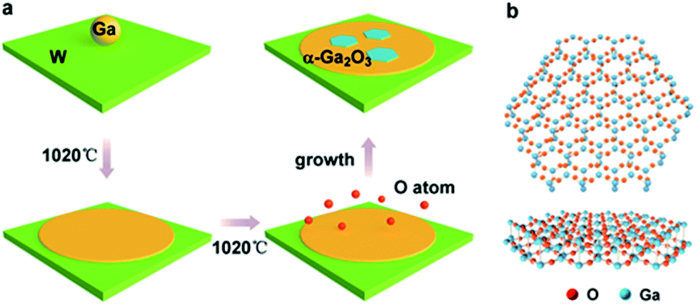 | ||
| Fig. 1 (a) Schematic of the α-Ga2O3 structure growth process. A drop of liquid Ga is placed on a W substrate. Then the Ga forms a flat surface owing to the good wetting behavior between Ga and the substrate as the temperature is increased. The O atoms diffuse to the surface of the liquid Ga to react and form hexagonal-shaped α-Ga2O3. (b) Crystal configuration of an α-Ga2O3 flake. | ||
The liquid gallium was then held at 1020 °C for 30 min; oxygen (10 sccm) was then pumped in to initiate the growth (Fig. S2†). During the process, the O atoms diffused to the liquid gallium surface with the carrier gas to react with liquid Ga to form Ga2O3 crystals. Finally, the sample is quickly moved out of the high temperature zone and rapidly cooled in the environment to retain the crystals. The crystal configuration of the simulated Ga2O3 crystal sheet is shown in Fig. 1b. It should be noted that the crystal form of gallium oxide is composed of a different arrangement of Ga atoms, resulting in different stacking of tetrahedral and octahedral ligands, which contributes to the phase stability as well as the optoelectronic properties of the polymorphs. In rhombohedral corundum α-Ga2O3, the Ga3+ ion ligand is only octahedral, and the cell volume is small.
To identify the morphology of the as-grown 2D Ga2O3, optical microscopy and scanning electron microscope (SEM) characterizations have been performed. The optical images are shown in Fig. 2a and S3a.† A SEM image of Ga2O3 is displayed in Fig. 2b. It is clearly observed that the as-grown Ga2O3 crystals are extremely uniform with respect to morphology and have regular hexagonal features. It is obviously detected that 2D hexagonal Ga2O3 crystals are dispersed on the whole surface, and the size is uniform, which is also confirmed by the transverse size statistics.
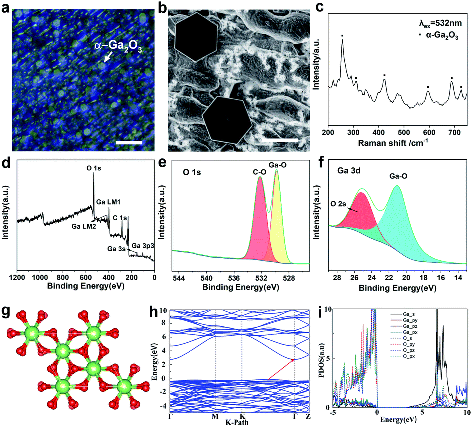 | ||
| Fig. 2 Characterization of the as-grown 2D ultrathin α-Ga2O3 crystals. (a) Optical image of α-Ga2O3 crystals on the liquid Ga surface. The image shows that the Ga2O3 crystals are hexagonal. (b) SEM image of hexagonal Ga2O3 crystals. (c) Raman spectrum of α-Ga2O3 crystals. (d–f) XPS measurements of hexagonal α-Ga2O3 single crystals. (g) Crystal structure of α-Ga2O3. (h) Band structure of α-Ga2O3. (i) Projected density of states (PDOS) of α-Ga2O3. The scale bars are 20 μm in (a) and 2 μm in (b). | ||
Fig. S3b† shows the statistical distribution of the flake lateral size, which mainly falls in the range of 4.5 ± 1 μm. In addition, it can be reasonably concluded from the optical photos that the hexagonal wafer is widely distributed and the surface of the hexagonal crystal is flat. Meanwhile, both optical photos and SEM images show that the substrate under the hexagonal wafer is not uniform. It is speculated that the oxidation of the liquid gallium surface in the air accounts for the phenomena. The thickness of the ultrathin crystal can be controlled by controlling the gas flow rate, and the relationship is shown in Fig. S4 and Table S1.† In our experiment, it was found that the liquid metal surface is flat at high temperature, and the growth of gallium oxide on this basis is conducive to transverse crystallization. The observed unevenness of the substrate is caused by solidification of the liquid substrate as it cools to the melting point. Therefore, the transverse growth of Ga2O3 crystals will not be impeded.
Raman spectroscopy was further performed on the as-grown hexagonal crystal as clearly displayed in Fig. 2c and S5a.† The characteristic Raman bands of Ga2O3 at 280, 425, 480, 595, 685, and 720 cm−1 are marked, further confirming the presence of α-Ga2O3.29 It has been acknowledged that when there is a tensile stress or compressive stress in the crystal, the atomic bond length will lengthen or shorten accordingly, which causes a change in the lattice constant. Therefore, the vibration frequency of the atom will change and then the peak of the Raman spectrum will move to a low wavenumber or high wavenumber.30 Furthermore, the compositional analysis of the Ga2O3 nanostructure was carried out by using X-ray photoelectron spectroscopy (XPS). The binding energies obtained from the XPS spectrum were corrected with the C 1s reference line at 284.6 eV. For the survey test of Ga2O3 shown in Fig. 2d, which reveals that the peaks of the core level from Ga 3p3, Ga 3s, C 1s, Ga LM1 Auger peak, Ga LM2 Auger peak and O 1s, and the peak of O 1s at 533 eV are related to the Ga–O bonds in the highest oxidation state of Ga (Fig. 2e and f). The binding energy values are in agreement with previously reported values.31 Energy dispersive X-ray spectroscopy (EDS) elemental mapping indicates a uniform distribution of Ga and O elements in the Ga2O3 crystal (Fig. S6†).
In order to understand the relationship between the structure and properties of gallium oxide in principle, we have made theoretical calculations. As a metastable phase in five isomers of Ga2O3, α-Ga2O3 has a corundum structure with two lattice parameters in the space group R3c. The structural parameters of optimized α-Ga2O3 (a supercell contains 12 Ga and 18 O atoms) are a = b = 5.06 Å, c = 13.62 Å, α = β = 90°, and γ = 120°, as shown in Fig. 2g. The electronic structures of α-Ga2O3 are calculated by using the first-principles method with the GGA-PBE functional. Our results revealed that α-Ga2O3 has indirect bandgaps of 2.92 eV (Fig. 2h). The projected density of states (PDOS) confirms the electronic structure of α-Ga2O3 (Fig. 2i). The valence band maximum (VBM) is mainly composed of O_p and Ga_p orbitals and the conduction band minimum is mainly composed of Ga_s and O_s orbitals. Due to more dispersity of s orbitals than p orbitals, it can be found that the effective mass of electrons is much smaller than that of holes.
In addition to discover the transverse growth of gallium oxide single crystals, the vertical growth of oxidizer crystals by controlling the content of oxygen was realized. A growth diagram was proposed to illustrate this growth phenomenon (Fig. 3a). In a CVD system filled with Ar at 1020 °C, oxygen diffused in the quartz tube onto the surface of gallium metal and catalyzed into O radicals (Fig. 3b). Consequently, O atoms are left behind to form Ga2O3 seeds. During this process, several nucleated seeds expand into islands (Fig. 3c). The relevant information has been reflected in Table S2.† The deposited atoms fall onto the substrate, where they first meet and bind together in a certain way to form groups of atoms. These already formed clusters are then added to by new atoms, allowing them to steadily grow into larger clusters that grow as the deposition process continues. There are irregular steps, deposited atoms, atomic groups, vacancies and islands existing in the surface of the material. Fig. 3b shows that the surface is very rough and has furrows, and their presence indicates that the surface is in a thermodynamic nonequilibrium state. Therefore, such a surface will relax to an equilibrium state whenever conditions permit. It is widely recognized that in many systems surface relaxation is achieved by atomic diffusion from island to island. This process is normally called Ostwald ripening.32 The islet has a higher chemical potential and the big island has a lower chemical potential, so there is a net flow of atoms from the islet to the big island. The island gradually shrinks and becomes smaller, and eventually degenerates and disappears. The process seems to be one where the big island grows and gradually the smaller islands merge.
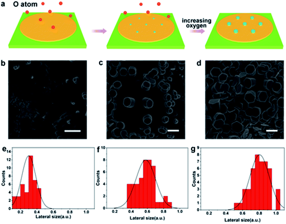 | ||
| Fig. 3 The shape evolution of the Ga2O3 that grows vertically. (a) Schematic showing the vertical growth mechanism of Ga2O3. (b–d) SEM images of vertical growth of hexagonal Ga2O3 crystals. (e–g) Lateral size distributions of the Ga2O3 crystal grown on Ga. The scale bars in (b), (c) and (d) are 1 μm. | ||
In our case, the diffusion rate of oxygen atoms is faster at higher flux and the content of oxygen atoms is relatively low in the reaction chamber. And that leads to lateral growth of gallium oxide crystals. Therefore, the low oxygen content makes the growth rate of gallium oxide crystals along the a and b axes greater than that along the c axis, so they appear as flake-like crystals. It is clearly found that the as-grown α-Ga2O3 crystals are extremely uniform with respect to morphology (Fig. 2d and e). However, when the gas flow rate is low, the oxygen free radicals diffusing to the surface of liquid gallium at high temperature have more chances to contact the metal gallium. At such a high concentration, the crystal of gallium oxide grows rapidly along the c axis, and the growth rate is higher than that in the a and b axes, so the phenomenon of vertical growth is presented (Fig. 3d and S7†). We can observe from the figure that, in the process of longitudinal growth of gallium oxide, its cross-sectional morphology has a certain evolution. At the early stage of growth, the cross section is nearly round, and gradually evolves into a regular hexagonal shape as the crystal grows with increasing growth time. The distribution statistics of the transverse dimensions in different stages of the longitudinal growth of gallium oxide have been shown (Fig. 3e–g). Fig. 3e shows that the cross-sectional size of the crystal is distributed around 0.3 ± 0.1 μm at the early stage of crystal growth. Fig. 3f shows that in the middle stage of crystal growth, the longitudinal growth of the crystal is more obvious and the transverse size increases to 0.6 ± 0.2 μm. Fig. 3g shows that after the crystal evolves into a regular hexagon, the cross-sectional size is distributed at 0.8 ± 0.2 μm. Those observations strongly indicate that the crystal grows both vertically and horizontally, consistent with the proposed growth mechanism as mentioned above.
In addition to the successful preparation of 2D α-Ga2O3 and vertical growth of α-Ga2O3, we also confirmed that the transformation of the gallium oxide crystal form from the α crystal phase to the β crystal phase can be realized by controlling the temperature at atmospheric pressure. Using the same method, we synthesized β-Ga2O3 nanobelts (Fig. 4). SEM observations reveal that the products consist of a large quantity of belt-type structures (Fig. 4a and S8a and b†), and the size of the sheets is about 10 μm across and several tens of nanometers in thickness. The nanobelts have straight edges with sharp corners, suggesting that they are terminated by faceted crystallographic planes.33 The range of the diameter of the as-grown nanobelts spans from 20 to 120 nm. The wavy and twisted shapes of the belts are apparent. The width of the belts varies from 40 to 300 nm, and the geometry of the belts is rather uniform. The thickness of the belts is 10 to 60 nm depending on the width. The unique structure of the nanobelts apparently indicates that their growth may be largely determined by growth kinetics. There are two common growth mechanisms for nanobelts. The vapor–liquid–solid (VLS) process was proposed for the nanobelts grown by a catalytic assisted technique,34,35 in which a metal particle is located at the growth front of the wire and acts as the catalytically active site. In the vapor–solid (VS) process, the oxide vapor, evaporated from the starting oxide at a higher temperature zone, directly deposits on a substrate at a lower temperature region and grows into ribbon-like nanostructures. The growth of the nanobelts might be dominated by the VS process, but we cannot totally rule out the VLS process because low melting point Ga metal particles are reduced in the synthesis, which may act as a catalyst for the growth. The formation of nanobelts is supposed to be a combined result of VLS and VS as well as growth kinetics.
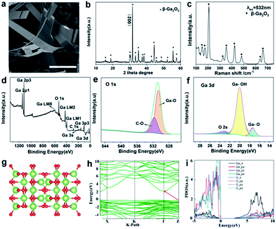 | ||
| Fig. 4 Characterization of β-Ga2O3 nanobelts. (a) SEM image of hexagonal β-Ga2O3 nanobelts. (b) XRD spectrum of β-Ga2O3. (c) Raman spectrum of the β-Ga2O3 crystal. (d–f) XPS results of β-Ga2O3 nanobelts. (g) Crystal structure of β-Ga2O3. (h) Band structure of β-Ga2O3. The Fermi energy is aligned to zero. (i) PDOS of β-Ga2O3. The scale bar in (a) is 10 μm. | ||
X-ray diffraction is used to elucidate the structural properties of the Ga2O3 nanosheets (Fig. 4b and S9†). The strongest peak is denoted as the (002) plane position, respectively. From the intensity variation in the diffraction pattern, we expect that the as-grown nanowires have different preferred growth directions. The phase structure of β-Ga2O3 is further investigated by using Raman spectroscopy (Fig. 4c). In the Raman spectrum of β-Ga2O3, peaks at 156, 182, 200, 318, 349, 417, 474, 629, and 653 cm−1 are observed. These peaks are characteristic of monoclinic Ga2O3.29 A typical XPS survey spectrum with energy ranging from 0 to 1200 eV obtained from β-Ga2O3 microspheres is shown in Fig. 4d; the characteristic peaks at 20 eV, 105 eV, 161 eV, 398 eV, 424 eV, 756 eV, 1118 eV, and 1144 eV can be assigned to Ga 3d, Ga 3p3, Ga 3s, Ga LM1, Ga LM2, Ga LM8, Ga 2p3 and Ga 2p1, respectively, revealing the peaks of the core level from Ga 3p3, Ga 3s, C 1s, Ga LM1 Auger peak, Ga LM2 Auger peak and O 1s. The energy peak of Ga 3d centered at 24.26 eV can be ascribed to the presence of gallium in β-Ga2O3 (Fig. 4f). The O 1s XPS signal observed at a binding energy of 531 eV corresponds to the characteristic peak of β-Ga2O3 (Fig. 4e). The XPS analysis indicates that the material synthesized was β-Ga2O3, which is consistent with the XRD measurement. The quantification of peaks reveals that the atomic ratio of Ga–O equals the stoichiometric ratio of 2![[thin space (1/6-em)]](https://www.rsc.org/images/entities/char_2009.gif) :3. Moreover, the binding energy values are in agreement with previously reported values.30 The structure and morphology of the Ga2O3 nanobelts were further characterized by transmission electron microscopy (TEM). Fig. S10† shows a low magnification TEM image showing a ribbon-like structure of β-Ga2O3. It can be observed that the nanobelts are long and straight. The nanobelts are single crystalline and free from dislocations.
:3. Moreover, the binding energy values are in agreement with previously reported values.30 The structure and morphology of the Ga2O3 nanobelts were further characterized by transmission electron microscopy (TEM). Fig. S10† shows a low magnification TEM image showing a ribbon-like structure of β-Ga2O3. It can be observed that the nanobelts are long and straight. The nanobelts are single crystalline and free from dislocations.
For optimized β-Ga2O3 (a supercell contains 8 Ga and 12 O atoms), these parameters are a = 5.06 Å, b = 3.04 Å, c = 5.83 Å, α = γ = 90°, and β = 103.70° (Fig. 4g). The electronic structures of β-Ga2O3 are calculated by using the first-principles method with the GGA-PBE functional (Fig. 4h), and β-Ga2O3 has indirect bandgaps of 2.34 eV. The projected density of states (PDOS) confirms that both α-Ga2O3 and β-Ga2O3 have similar electronic structures (Fig. 4i). It is noted that α-Ga2O3 has a larger bandgap than β-Ga2O3. This is attributed to the stronger orbital coupling in α-Ga2O3 due to its smaller volume per unit cell (47.81 Å3 for α-Ga2O3 and 52.49 Å3 for β-Ga2O3). For both α-Ga2O3 and β-Ga2O3, the VBMs have bonding state characters and the CBMs are mainly anti-bonding states. The VBM (bonding states) will shift down and the CBM (anti-bonding states) will shift up when the Ga–O bond length is shorter (in α-Ga2O3), resulting in a wider bandgap in α-Ga2O3. It should be noted that Ga2O3 is an ultrawide-band-gap, transparent, semiconducting oxide material. Its band gaps of 4.5–5.3 eV depend on its crystal structure. There are five main phases of Ga2O3 (α-, β-, γ-, δ- and ε-), of which β-Ga2O3 is the most stable phase and has received extensive attention and research. For β-Ga2O3, the band gap was experimentally reported to be 4.7–4.9 eV. In addition to β-Ga2O3, the second stable α-Ga2O3 is also suitable for solar-blind UV detector applications with its large bandgap of nearly 5.2 eV.
In summary, we demonstrate the successful growth of highly crystalline 2D α-Ga2O3 single crystals on liquid Ga via the sublimation of O atoms by the CVD method. The size distribution of the obtained single crystal is uniform, and the shape is regular and hexagonal. By controlling the growth time, the vertical growth of the single crystal is realized. β-Ga2O3 nanosheets were further prepared by controlling the growth temperature and realizing the transformation of the crystal phase. Our strategy paves a new route to produce 2D ultrathin Ga2O3 with a large lateral size. Their relatively direct large bandgap characters suggest that they hold substantial promise for future nanoelectronics.
Conflicts of interest
There are no conflicts to declare.Acknowledgements
The authors acknowledge funding from the National Natural Science Foundation of China (Grant 52002267).Notes and references
- C. Liu, L. Wang, J. J. Qi and K. H. Liu, Adv. Mater., 2020, 32, 2000046 CrossRef CAS PubMed.
- X. Tong, K. L. Liu, M. Q. Zeng and L. Fu, InfoMat, 2019, 1, 460–478 CrossRef CAS.
- C. Xu, L. B. Wang, Z. B. Liu, L. Chen, J. K. Guo, N. Kang, X. L. Ma, H. M. Cheng and W. C. Ren, Nat. Mater., 2015, 14, 1135–1141 CrossRef CAS PubMed.
- M. Y. Li, S. K. Su, H. S. P. Wong and L. J. Li, Nature, 2019, 567, 169170 Search PubMed.
- A. Chaturvedi, B. Chen, K. Zhang, Q. He, G. H. Nam, L. You, Z. Lai, C. Tan, T. H. Tran, G. Liu, J. Zhou, Z. Liu, J. Wang, E. H. T. Teo and H. Zhang, SmartMat, 2020, 1, e1011 CrossRef.
- Y. X. Fan, L. Li, G. Yu, D. C. Geng, X. T. Zhang and W. P. Hu, Adv. Mater., 2020, 33, 2003956 CrossRef PubMed.
- C. L. Tan, X. H. Cao, X. J. Wu, Q. Y. He, J. Yang, X. Zhang, J. Z. Chen, W. Zhao, S. K. Han, G. H. Nam, M. Sindoro and H. Zhang, Chem. Rev., 2017, 117, 6225–6331 CrossRef CAS PubMed.
- B. Wu, D. C. Geng, Y. L. Guo, L. P. Huang, Y. Z. Xue, J. Zheng, J. Y. Chen, G. Yu, Y. Q. Liu and L. Jiang, Adv. Mater., 2011, 23, 3522–3525 CrossRef CAS PubMed.
- S. M. Kim, A. Hsu, M. H. Park, S. H. Chae, S. J. Yun, J. S. Lee, D. H. Cho, W. J. Fang, C. Lee and T. Palacios, Nat. Commun., 2015, 6, e8662 CrossRef PubMed.
- C. S. Lau, J. Y. Chee, Y. S. Ang, S. W. Tong, L. Cao, Z. Ooi, T. Wang, L. K. Ang, Y. Wang, M. Chhowalla and K. E. J. Goh, ACS Nano, 2020, 14, 13700–13708 CrossRef CAS PubMed.
- Z. Wang, R. Li, C. Su and K. P. Loh, SmartMat, 2020, 1, e1013 Search PubMed.
- A. Zavabeti, J. Z. Ou, B. J. Carey, N. Syed, R. Orrell-Trigg, E. L. H. Mayes, C. Xu, O. Kavehei, A. P. O'Mullane, R. B. Kaner, K. Kalantar-zadeh and T. Daeneke, Science, 2017, 358, 332–335 CrossRef CAS PubMed.
- B. Y. Zhang, K. Xu, Q. F. Yao, A. Jannat, G. H. Ren, M. R. Field, X. M. Wen, C. H. Zhou, A. Zavabeti and J. Z. Ou, Nat. Mater., 2021 DOI:10.1038/s41563-020-00899-9.
- S. S. Zhao, J. Q. Zhang and L. Fu, Adv. Mater., 2021, 33, 2005544 CrossRef CAS PubMed.
- A. Lipatov, M. Alhabeb, H. D. Lu, S. S. Zhao, M. J. Loes, N. S. Vorobeva, Y. Dall'Agnese, Y. Gao, A. Gruverman, Y. Gogotsi and A. Sinitskii, Adv. Electron. Mater., 2020, 6, 1901382 CrossRef CAS.
- Y. L. Hong, Z. B. Liu, L. Wang, T. Y. Zhou, W. Ma, C. Xu, S. Feng, L. Chen, M. L. Chen, D. M. Sun, X. Q. Chen, H. M. Cheng and W. C. Ren, Science, 2020, 369, 670–674 CrossRef CAS PubMed.
- S. M. Li, M. C. Tian, Q. G. Gao, M. F. Wang, T. Y. Li, Q. L. Hu, X. F. Li and Y. Q. Wu, Nat. Mater., 2019, 18, 1091–1094 CrossRef CAS PubMed.
- G. Yang, S. Jang, F. Ren, S. J. Pearton and J. Kim, ACS Appl. Mater. Interfaces, 2017, 9, 40471–40476 CrossRef CAS PubMed.
- Y. F. Sun, Q. H. Liu, S. Gao, H. Cheng, F. C. Lei, Z. H. Sun, Y. Jiang, H. B. Su, S. Q. Wei and Y. Xie, Nat. Commun., 2013, 4, e2899 CrossRef PubMed.
- M. Handwerg, R. Mitdank, Z. Galazka and S. F. Fischer, Semicond. Sci. Technol., 2016, 31, 125006 CrossRef.
- S. J. Pearton, J. C. Yang, P. H. Cary, F. Ren, J. Kim, M. J. Tadjer and M. A. Mastro, Appl. Phys. Rev., 2018, 5, 011301 Search PubMed.
- Z. Galazka, K. Irmscher, R. Uecker, R. Bertram, M. Pietsch, A. Kwasniewski, M. Naumann, T. Schulz, R. Schewski, D. Klimn and M. Bikermann, J. Cryst. Growth, 2014, 404, 184–191 CrossRef CAS.
- T. Watahiki, Y. Yuda, A. Furukawa, M. Yamamuka, Y. Takiguchi and S. Miyajima, Appl. Phys. Lett., 2017, 111, 222104 CrossRef.
- J. Su, T. Liu, J. M. Liu, J. Yang, G. Y. Shen, Y. B. Bai, Z. Y. Dong and Y. W. Zhao, J. Semicond., 2016, 37, 103004 CrossRef.
- K. D. Leedy, K. D. Chabak, V. Vasilyev, D. C. Look, J. J. Boeck, J. L. Brown, S. E. Tetlak, A. J. Green, N. A. Moser, A. Crespo, D. B. Thomson, R. C. Fitch, J. P. McCandless and G. H. Jessen, Appl. Phys. Lett., 2017, 111, 012103 CrossRef.
- L. Nagarajan, R. A. De Souza, D. Samuelis, I. Valov, A. Borger, J. Janek, K. D. Becker, P. C. Schmidt and M. Martin, Nat. Mater., 2008, 7, 391–398 CrossRef CAS PubMed.
- M. Wurdack, T. H. Yun, E. Estrecho, N. Syed, S. Bhattacharyya, M. Pieczarka, A. Zavabeti, S. Y. Chen, B. Haas, J. Muller, M. N. Q. L. Bao, C. Schneider, Y. R. Lu, M. S. Fuhrer, A. G. Truscott, T. Daeneke and E. A. Ostrovskaya, Adv. Mater., 2021, 33, 2005732 CrossRef CAS PubMed.
- Y. Saito, T. Nojima and Y. Iwasa, Nat. Rev. Mater., 2017, 2, 16094 CrossRef CAS.
- D. Machon, P. F. McMillan, B. Xu and J. Dong, Phys. Rev. B: Condens. Matter Mater. Phys., 2006, 73, 094125 CrossRef.
- G. Gouadec and P. Colomban, Prog. Cryst. Growth Charact. Mater., 2007, 53, 1–56 CrossRef CAS.
- J. H. Zhang, S. J. Jiao, D. B. Wang, S. Y. Gao, J. Z. Wang and L. C. Zhao, Appl. Surf. Sci., 2021, 541, 148380 CrossRef CAS.
- R. F. Li, Z. T. Luo and F. Papadimitrakopoulos, J. Am. Chem. Soc., 2006, 128, 6280–6281 CrossRef CAS PubMed.
- Y. H. Wang, L. Hou, X. J. Qin, S. D. Ma, B. Zhang, H. Y. Gou and F. M. Gao, J. Phys. Chem. C, 2007, 111, 17506–17511 CrossRef CAS.
- F. Litimeina, D. Racheda, R. Khenatab and H. Baltacheb, J. Alloys Compd., 2009, 488, 148–156 CrossRef.
- Z. R. Dai, Z. W. Pan and Z. L. Wang, J. Phys. Chem. B, 2002, 106, 902–904 CrossRef CAS.
Footnote |
| † Electronic supplementary information (ESI) available. See DOI: 10.1039/d1na00375e |
| This journal is © The Royal Society of Chemistry 2021 |