
 Open Access Article
 This Open Access Article is licensed under a Creative Commons Attribution-Non Commercial 3.0 Unported Licence
Near-IR emission of InGaN quasi-quantum dots on non-polar GaN nanowire structures
Dae-Young
Um†
a,
Yong-Ho
Ra†
b,
Ji-Hyeon
Park
b,
Ga-Eun
Hong
a and
Cheul-Ro
Lee
 *a
*a
aSemiconductor Materials & Process Laboratory (SMPL), School of Advanced Materials Engineering, Engineering College, Research Center for Advanced Materials Development (RCAMD), Jeonbuk National University (JBNU), Jeonju 54896, Republic of Korea. E-mail: crlee7@jbnu.ac.kr
bOptic & Electronic Component Material Center, Korea Institute of Ceramic Engineering & Technology, Jinju 52851, Republic of Korea
First published on 9th July 2021
Abstract
In group III-nitride based semiconductor structures, the incorporation of high-indium-composition InGaN has been severely limited by extremely inefficient strain-induced polarization fields and prohibitively large defect densities. So far, there is no clear approach to solve this issue. Here, we have shown a new approach to incorporate high concentrations of indium in the InGaN structure by using a non-polar quasi-quantum dot heterostructure. This unique epitaxial growth was achieved by integrating a 1-dimensional nanowire and a 0-dimensional quantum dot structure using an MOCVD system. The formation of a high-efficiency quantum-sliding heterostructure and high-quality nanowire structure was confirmed by FE-SEM and TEM measurements. Furthermore, it has been suggested that such a quantum-dot structure can dramatically improve radiative recombination through a new sliding bandgap mechanism. We also found that non-polar quantum dots can not only incorporate more indium than conventional multi-quantum well structures grown on the nanowire structure, but also significantly improve crystalline quality. The PL results verified that the wavelength of quantum dots fabricated on the nanowire structure can easily shift up to 913 nm. The first demonstration in the integration of nanowire and quantum dot structures will open a new avenue to break through the limitations of high indium incorporation in photonic semiconductor systems.
1. Introduction
Over the past few decades, III–V compound semiconductor materials have been widely used in optoelectronics and photonics applications, due to their excellent optical and structural properties. In particular, nitride and arsenide based materials have been developed and realized for photonic device applications, such as light emitting diodes (LEDs), lasers, photodetectors and solar cells.1,2 In GaN-based epitaxial structures, the c-plane piezoelectric polarization field significantly affects the optical and electrical properties, and consequently limits the improvement of LED efficiency.3,4 Until recently, with the increasing demand for more highly efficient blue and white LEDs, a lot of work has been done to develop more advanced GaN-based quantum heterostructures. Various effective approaches have been tried to overcome the limitations, such as the use of the unique heterogeneous LED structure.3–5 Nanowire (NW) structures are one of the technologies to solve this issue, and have attracted a lot of attention over the past few years to improve LED device performance.6–8Since the GaN-based NW structure has tremendous advantages, including a wide direct band gap (3.4 eV), high thermal conductivity (1.3 W cm−1 K−1), extremely fast electron velocity, and excellent physical and chemical stability, it can be greatly useful for improving optoelectronic efficiency.9–13 Several groups have reported on the incorporation of two-dimensional (2-D) multi-quantum well (MQW) on GaN NW structures to improve the LED device performance.14–17 Blue-emitting InGaN/GaN MQW LEDs have also been demonstrated.18–21 However, in the case of quantum well structures, the two-dimensional continuous state allows more phonon-mediated scattering processes, shortening the carrier lifetime, and as a result, it is impossible to overcome the so-called green gap problem due to the very poor crystal quality, which is related to large defect densities due to the high lattice mismatch ratio between high x (x > 0.3) InxGa1−xN and GaN.22 Alternatively, it can be expected that the 3D quantum dot (QD) and pyramid (QP) structures not only have a better quantum confinement structure, but also have more surface strain relaxation than the 2D quantum well structure.23 Most studies involved the growth of InGaN QDs and QPs on GaN film structures.24,25 Deshpande et al. reported that InGaN QDs grew on AlGaN NWs, while Bi et al. reported the growth of InN QDs on top of GaN NWs.26,27 The optical characteristics of InGaN QDs grown on GaN pyramidal arrays were reported by Hsu et al.28 They showed that although the 3D quantum structures contributed to improving the light efficiency of LEDs, there is still great difficulty in increasing the high indium content in the InGaN structure. A non-polar m-plane in GaN is well known as a structure capable of completely terminating the polarization fields. And it was confirmed that the nanowire structures can dramatically reduce the defect densities due to the surface strain relaxation. 3D quantum structures have a much superior quantum confinement structure than 1D or 2D structures. It is expected that improved crystal quality and higher indium incorporation can be achieved by the development of new heterostructures through the combination of nanowires, 3D quantum structures, and non-polar m-plane structures.29,30 In addition to fabricating high x InxGa1−xN QPs densely formed on the nonpolar surfaces of GaN NWs, we established a new approach to energy bandgap engineering for better inducing of radiative recombination in the regions with good crystallinity.
However, the growth of 1-D nanostructures of the ternary compound semiconductor AlxGa1−xN system with a tunable band gap of 3.4–6.2 eV has been limited by the complex multi-component phase diagram and inhomogeneous composition distribution. A few 1-D AlxGa1−xN nanostructures have been synthesized using chemical vapor deposition (CVD), metal–organic chemical vapor deposition (MOCVD) and molecular beam epitaxy (MBE).23–29 In the past, the other researchers synthesized AlxGa1−xN nanowires over the whole compositional range by the CVD technique using Al/Ga/NH3 as source materials. And, previous work have shown the growth of AlGaN nanocones across the complete composition range by CVD using AlCl3/GaCl3/NH3 as raw materials. Also, previous report have presented the evolution of various GaN nanostructures depending on the MOCVD growth parameters.31 In addition, optoelectronic devices have also been realized utilizing MBE grown AlGaN nanowires operating in the UV-C region.32–34 Despite these intensive studies, the controlled synthesis of vertically aligned compositionally uniform 1-D AlxGa1−xN nanorods (NRs) still remains challenging for extensive optoelectronic applications, particularly in ultraviolet light emitters and photodetectors. Further experimental study is required to realize the controlled fabrication of vertically aligned 1-D AlxGa1−xN nanostructures. Moreover, photoconductive AlGaN nanorod based UV-C photodetectors with simple device structures have not been reported.
In this study, we have, for the first time, demonstrated a new integrated development of 3D quantum structures and m-plane 1D nanowire structures using the unique pulse mode technique of the MOCVD system. A new 3D quantum pyramid structure was designed based on new sliding bandgap engineering through a pyramid-like epitaxial structure grown on a nanowire. We have also shown that the 3D quantum pyramid structure can change the wavelength from blue emission to ∼913 nm. Compared to the typical MQW structure, the emission intensity and spectral linewidth of QPs are greatly improved due to the dramatically reduced defect density. From field-emission scanning electron microscopy (FE-SEM), transmission electron microscopy (TEM), energy dispersive X-ray spectroscopy (EDX), cathodoluminescence (CL), and photoluminescence (PL) analysis, it was confirmed that the improved radiative recombination rate was related to the localized quantum effects in QPs formed by incorporation of different indium amounts. We also found that non-polar quantum dots can not only incorporate more indium than conventional multi-quantum well structures grown on the nanowire structure, but also significantly improve crystalline quality.
2. Experimental section
The growth procedure of the quantum heterostructures is schematically shown in Fig. 1a. In the first step, n-GaN NWs were initially grown on the n-Si (111) substrate via a 3-step growth mode using the MOCVD technique. Detailed growth conditions and processes can be found in our previous paper.31 The nanowires were grown in the c-plane direction, but the six sides of the nanowires consist of non-polar m-planes. The n-GaN NW length is about 3 to 4 μm, the diameter is 200 to 300 nm, and the density is high. In the second step, high x InxGa1−xN QPs were coaxially grown on the nonpolar surface of n-GaN NWs via Stranski–Krastanov (SK) growth. In general, during the MOCVD growth, indium is very easily desorbed at high temperatures. A lower temperature was introduced to enhance the incorporation of indium into InxGa1−xN QPs. On the other hand, at too low temperatures, the cracking of ammonia does not occur properly. Therefore, the optimal temperature for synthesizing InxGa1−xN QPs emitting near-infrared (near-IR) with sufficient ammonia cracking and high indium incorporation was obtained at the temperature range from 600 °C to 500 °C. In order to increase the indium composition along the growth direction of the quantum pyramid structures, the substrate temperature was gradually ramped down from 600 °C to 500 °C during the entire growth period, while maintaining the chamber pressure of 600 torr. The gas flow rates of trimethylgallium and trimethylindium were used at 0.1 sccm and 10 sccm, respectively. For the high indium incorporation, the pulse mode growth process was performed in 30 pairs for 1 min each. Here, the ammonia flow rate was kept as 5 slm with continuous mode for the 30 pair growth. The reason why the ammonia flow is not in pulsed mode is that epitaxial growth performs the process at a relatively low temperature where ammonia decomposition is somewhat difficult. Consequently, this is to induce the decomposition of as much ammonia as possible. The overall process conditions for fabricating nanostructures with various indium compositions described above are outlined in Fig. 2. | ||
| Fig. 1 (a) Schematic illustration of the high x InxGa1−xN QP structures coaxially grown on a GaN NW template by the MOCVD technique. Schematic representation of (b) the coaxial distribution of InGaN QPs formed on GaN NWs, and (c) the formation planes of InGaN QPs. (d) FE-SEM image of InGaN quantum-heterostructures grown on the Si (111) substrate by the MOCVD technique. (e) High-magnification FE-SEM image of the surface corresponding to the region of the formed QPs. | ||
 | ||
| Fig. 2 Schematically illustrated representation of the experimental process conditions corresponding to especially unique energy bandgap engineering for fabricating high x InxGa1−xN QPs having indium variation with gradationally decreasing energy bandgaps by using a GaN NW template via a pulsed-mode MOCVD system. | ||
3. Results and discussion
The high x InxGa1−xN QP nanostructures in the last growth step were grown mainly in the non-polar region of n-GaN NWs, as shown in Fig. 1b. It can be seen that these nanostructures grown coaxially in NWs have three and one surfaces corresponding to r and c surfaces, respectively, as shown in Fig. 1c. From the FE-SEM results shown in Fig. 1d and e, it can be clearly confirmed that the QPs having four sides were grown on the non-polar surfaces of the nanowires with very high densities. The nanostructures were measured to have an average diameter of ∼100 nm and an average height of ∼50 nm, respectively. From the FE-SEM image, we counted the number of QPs formed on six m-planes of the nanowire. The density of QPs formed on the coaxial nanowire surface can be estimated to be ∼222 × 108 cm−2. It can be expected that this QP structure formed at high density on the non-polar surface of NWs will show very excellent luminous performance when applied as an optoelectronic device. To confirm the elemental distributions, EDX analysis was performed with the quantum-heterostructure nanowires. As confirmed from the EDX line profile in Fig. 3 (corresponding to Fig. 3a) and the EDX elemental mapping data (corresponding to Fig. 3b and b-1–b-3), indium, gallium, and nitrogen are well distributed in the nanostructure. We noticed that the concentration of indium in a single nanowire increased from the bottom to the top. These various compositions of indium along the length of the single nanowire suggest the possibility of realizing multi-color emission wavelengths in the single nanowire structure. The distribution of gallium and nitrogen was uniformly detected in the entire nanowire area, while indium was detected locally only in the QP-formed area. | ||
| Fig. 3 (a) FE-SEM image of a single nanowire corresponding to the quantum-heterostructure with high x InxGa1−xN QPs. EDX elemental mapping profile image corresponding to (b) the overall ternary elements including (b-1) indium, (b-2) gallium, and (b-3) nitrogen. | ||
In order to identify the coaxial InxGa1−xN QP quantum-heterostructures grown on the GaN nanowire, we have further performed detailed TEM analysis using a JEOL-JEM-2010 equipped with an emission gun operated at 200 kV, shown in Fig. 4. The sample was prepared along the <0001> growth direction of the nanowire by a dual beam-focused ion beam (FIB, Quanta 3D FEG) system with a resolution of 7 nm @ 30 kV. Fig. 4a shows the scanning TEM (STEM) image which is measured at an electron beam diameter of ∼0.5 nm. The InxGa1−xN QP structures grown on the side of GaN NWs are clearly observed. As is well known, nanostructures based on wurtzite-GaN have a pyramid-shaped tip due to the Ga-polar termination.35 Our results suggest that not only does the tip of the GaN nanowire but also the InxGa1−xN QP have a pyramidal shape, so it can be expected to have a Ga-polar termination. No noticeable defects, indium clusters, or extended dislocations were observed in the quantum-pyramid heterostructures, shown in Fig. 4a and b. At marker “1” shown in the high-resolution STEM image of Fig. 4b, we confirmed the presence of a lattice image corresponding to the initial growth area of InxGa1−xN QP and the presence of stacking faults due to a high lattice mismatch ratio. In addition, as shown in the right panel corresponding to the point-“2” spot of Fig. 4b, it can be clearly observed that the interface exists in the lattice image due to the high indium composition in the region where the nanostructures begin to grow. As shown in point-“3”, a representative selected area electron diffraction (SAED) pattern demonstrates the formation of a wurtzite-hexagonal structure with (0002), (01![[1 with combining macron]](https://www.rsc.org/images/entities/char_0031_0304.gif) 0), and (01) diffraction spots originating from the atomic spacings of InGaN and GaN structures, respectively. Furthermore, the high-resolution STEM EDX mapping profiles showed the distribution of indium, gallium, and nitrogen from the regions (in Fig. 4(b-1–b-3)). In particular, high indium distribution in the InxGa1−xN QP, as shown in Fig. 4b-1 and b-2, was observed mainly in the last growth region compared to gallium element. These results prove that new types of quantum-heterostructure can be fabricated through our unique pulsed mode MOCVD growth technique, and the quantum-heterostructures fabricated in this approach prove that the indium content can also be effectively controlled.
0), and (01) diffraction spots originating from the atomic spacings of InGaN and GaN structures, respectively. Furthermore, the high-resolution STEM EDX mapping profiles showed the distribution of indium, gallium, and nitrogen from the regions (in Fig. 4(b-1–b-3)). In particular, high indium distribution in the InxGa1−xN QP, as shown in Fig. 4b-1 and b-2, was observed mainly in the last growth region compared to gallium element. These results prove that new types of quantum-heterostructure can be fabricated through our unique pulsed mode MOCVD growth technique, and the quantum-heterostructures fabricated in this approach prove that the indium content can also be effectively controlled.
 | ||
| Fig. 4 (a) A low-magnification bright field (BF) STEM image, and (b) high-magnification high angle annular dark field (HAADF) STEM image of a high x InxGa1−xN QP NW taken along the <20> zone axis. The lattice fringe image of the initial growth region (point-“1”) near the surface of GaN, of the interface (point-“2”) between high x InxGa1−xN and GaN. SAED pattern (point-“3”), which exhibits the high-quality wurtzite-hexagonal InGaN/GaN structure with (0002), (010), and (01) diffraction spots and <0001> growth direction along the c-plane. (b-1 to b-3) TEM EDX elemental mapping profile image of the quantum-heterostructure. Indium element is strongly present in the later growth region. | ||
We have further performed EDX line profile and point profile analysis using a high-resolution STEM system to obtain a more detailed elemental distribution in the nanostructures, shown in Fig. 5. Fig. 5a-1 (in the “green square” area in Fig. 5a) shows the tendency for the indium composition to gradually increase along the growth direction, but the gallium composition gradually decreases. From the overall EDX line profile of the nano-pyramid it can be seen that the gallium and indium change linearly. Also, in Fig. 5b-1 (“red square” area in Fig. 5b), the indium composition in the nanostructures was 43%, 58%, and 68% at each point (-“1”, -“2” and -“3”). These results show that high indium synthesis, which was previously extremely challenging, can be realized by our unique pulse mode MOCVD growth method. Interestingly, the unique indium imbalance in the nano-pyramidal structure suggests the formation of a new quantum well structure in the pyramid structure.
 | ||
| Fig. 5 A low-magnification high angle annular dark field (HAADF) STEM image corresponding to (a) a region near the top, and (b) a region near the bottom of the high x InxGa1−xN (with indium variation) nanowire heterostructure. A high-magnification TEM EDX elemental (a-1) line profile image, and (b-1) point profile image of high x InxGa1−xN QP having indium variation corresponding to a “green-square” and “red-square” each. The sloping indium composition from ∼43% to ∼68% (corresponding to point-“1”, -“2”, and -“3”) along the growth direction of the high x InxGa1−xN QP having indium variation. | ||
From the different compositions of indium in the pyramid structure in Fig. 5, we have designed a new quantum-sliding energy bandgap structure schematically shown in Fig. 6. Fig. 6a shows an energy band diagram of the i-InxGa1−xN/n-GaN quantum-heterostructure. With the unique pyramidal nanostructure with various indium compositions, the radiative recombination mechanism is introduced in a localized quantum area by a gradationally decreasing energy bandgap. For this energy band diagram, the electron–hole-pairs (EHPs) generated by a specific excitation energy can slide down the conduction and valence bands towards lower energy levels within the lifetime. As a result, radiative recombination will occur in the local quantum region at the tip of the pyramid with the lowest energy band gap of the quantum-heterostructure. Based on this hypothetical mechanism, we decided to call this local area “quasi-QD” where radiative recombination can mainly occur, shown in Fig. 6b. It is expected that the reduction in luminous efficiency through the non-radiative recombination of the trap level formed in the near-interface region can dramatically improve the efficiency through the energy bandgap sliding effect at the end of the pyramid formed with high crystallinity in the QP. In general, the trap level can be caused by various defects such as dislocations, vacancies, stacking defects, etc. due to a very high lattice mismatch between the high x InxGa1−xN QP and GaN NW. However, the high quality pyramidal quasi-QD tips, formed by the surface strain relaxation effect, can dramatically reduce these trap levels, and significantly increase the radiative recombination rate. In addition, the effective 3D indium incorporation in the m-plane structure can realize wavelengths beyond the red wavelength to the near-IR wavelength range, so it can be very useful for optical devices operating in high-indium-composition InGaN.
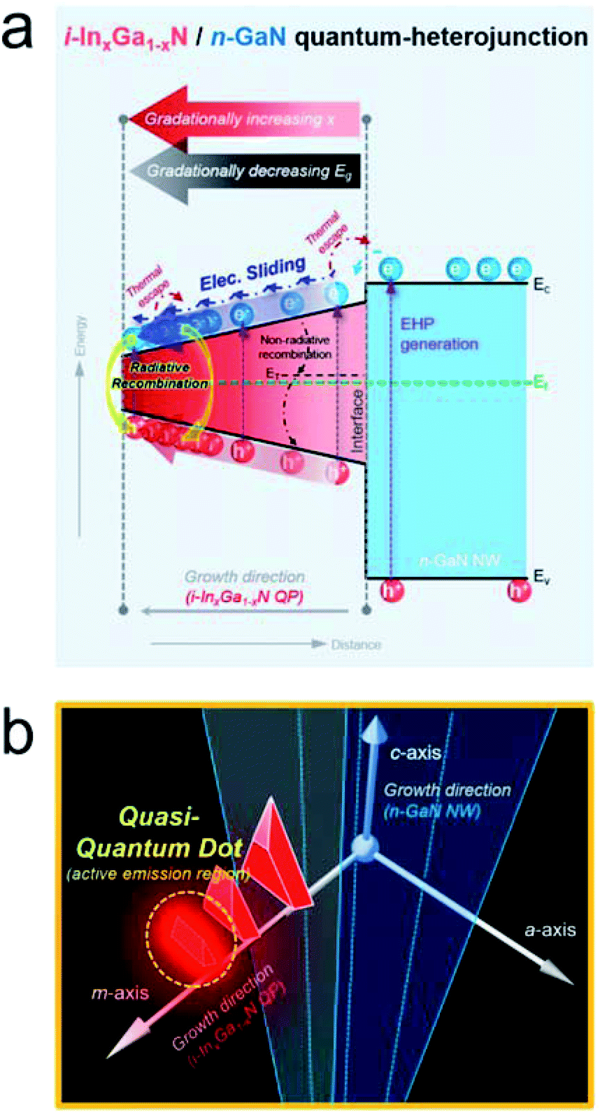 | ||
| Fig. 6 (a) Schematic illustration of the energy bandgap diagram of the i-InxGa1−xN/n-GaN quantum-heterostructure with gradationally decreasing energy bandgap to induce radiative recombination of generated EHPs by using the unique mechanism. (b) Schematically illustrated representation of the structure related to the active emission region named quasi-QD in high x InxGa1−xN having indium variation. | ||
The optical properties of the nanowires used as the first-step surface strain relaxation structure were studied by temperature-dependent CL measurement. Fig. 7a shows the CL spectra measured at temperatures of 78 K and 300 K. The wavelength peaks at 355 and 365 nm correspond to the optical properties of the GaN wurtzite hexagonal-structure, and the blue shift of about 10 nm is consistent with well-known results from previous reports such as thermal transitions.32 The energy band gaps measured at 78 and 300 K correspond to 3.492 and 3.397 eV, respectively. The linewidth of the wavelength is very narrow, which proves that despite the large lattice mismatch of the Si (111) substrate and GaN, the GaN nanowires were grown to very high crystallinity due to the surface relaxation effect. Fig. 7b shows the FE-SEM image of the InGaN QPs grown on the GaN NW structure, and the inset in Fig. 7a shows a CL mapping image measured at 365 nm wavelength from Fig. 7b. The CL mapping image shows that only the nanowire pillars emit light corresponding to the 365 nm wavelength.
 | ||
| Fig. 7 (a) CL spectra of GaN NWs with InxGa1−xN QPs measured at low temperature and room temperature corresponding to 78 K and 300 K each. Inset: CL mapping image of GaN NWs with InxGa1−xN QPs spectrally resolved under 365 nm at 300 K. (b) FE-SEM image of a single GaN NW with InxGa1−xN QPs. | ||
Additionally, temperature-dependent PL measurement was also performed to analyze the optical properties of the high x InxGa1−xN QPs which have a non-polar surface quasi-QD structure, shown in Fig. 8. Fig. 8a shows that the emission wavelengths of the high x InxGa1−xN QPs (with quasi-QDs) range from ∼800 nm to ∼1000 nm, and that the main emission peak corresponds to ∼915 nm at room temperature. With very high indium concentrations, the broad wavelength peaks may be due to the formation of various bandgap energies caused by various nanoparticle sizes.33 In the PL results, no emission wavelength for about 40% indium composition (the expected wavelength is around 650 nm) measured by EDS was found. As hypothesized above, it can be inferred that electron and hole carriers moved to a lower energy level due to the energy band sliding effects. In addition, we have further studied temperature-dependent PL measurements from 88 K to 300 K in order to determine the more detailed optical properties. The QP sample exhibited a wavelength of about 913 nm at 88 K, and upon increasing the temperature to 300 K, it showed a wavelength of about ∼915 nm with a blue shift, shown in Fig. 8b–d. This is expected based on both previous reports and the well-known Varshni's law with increasing temperature.32,34 Based on the Gaussian fitting values of the PL spectrum, the FWHM values were calculated at 300 K to be ∼177.97 meV and at 88 K to be ∼125.47 meV, respectively, shown in Fig. 8c and d. Regarding the reason for multiple wavelengths with different measured temperatures, pyramid-structured quantum dots are fabricated by multi-InxGa1−xN layers formed from various indium compositions under gradationally ramping-down temperature during the growth. These different InxGa1−xN layers will cause various excitations with measured-temperature changes. To the best of our knowledge, this is a new record value not reported in previous studies in a similar indium content and wavelength range.27,36–38 Typically, when the indium composition is increased in the InxGa1−xN material, the defect density is dramatically increased due to the indium impurity and the lattice mismatch between InxGa1−xN and GaN, which causes an increase in the FWHM. In particular, it is common to show a FWHM greater than ∼100 nm over a wavelength of ∼600 nm. Here, we have reported an improved result of ∼90 nm at a wavelength of ∼900 nm. This is mainly due to the formation of InxGa1−xN quasi-QDs synthesized step by step at low growth temperature and surface relaxation of defects by the QPs through the newly introduced pulsed MOCVD technique. As shown in the experimental results, for near-IR emission, our optimized QP formation was obtained in the growth temperature range of 500 to 600 °C. Based on these optimized conditions, we adjusted the wavelength emissions by effectively controlling the concentration of indium contained in InxGa1−xN QPs. In addition, because indium generally does not participate in the formation of InxGa1−xN compounds by causing desorption of most indium adatoms at high growth temperature, it may also be possible to realize the various InxGa1−xN QPs emitting at visible wavelengths above the green-gap by modulation of growth temperature. We believe that this tremendous improvement in linewidth and wavelength is due to the dramatic reduction in defect densities as well as newly formed three-dimensional quantum well structures.
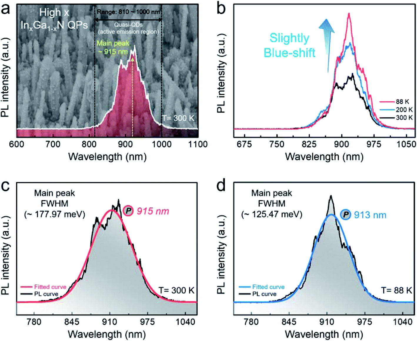 | ||
| Fig. 8 (a) PL spectrum of quantum-heterostructures (with high density) including high x InxGa1−xN QPs (with various size distributions) having quasi-QDs corresponding to the main active region for inducing radiative recombination of generated EHPs. (b) Temperature-dependent PL study of quantum-heterostructures from 88 K to 300 K, respectively. PL spectrum with a Gaussian fitted curve which represents both the main peak wavelength and FWHM at (c) 300 K and (d) 88 K, respectively. | ||
The excellent optical properties of high x InxGa1−xN QPs with quasi-QDs can be explained by the mechanisms involved in the formation of unique strain relaxation nanostructures, as schematically shown in Fig. 9. By increasing the indium composition in the InGaN structure, InGaN causes a greater lattice mismatch with the GaN structure, which leads to an enormous density of defects, shown in Fig. 9a and b. In our approach by integrating the nanowire and nano-pyramidal structures, firstly, all threading dislocation defects arising from the substrate can be terminated through the nanowire structure. Secondly, as shown in Fig. 9c, the nano-pyramidal structure grown on the non-polar m-plane side of the nanowires can effectively relax the defects to the surface. Moreover, the gradually increasing indium composition from the GaN nanowire interface can also effectively solve the lattice mismatch issues. This two-step strain relaxation technique will open a new avenue for long wavelength realization and low-defect high indium synthesis.
 | ||
| Fig. 9 (a) Schematically illustrated representation of the high lattice mismatch ratio between high x (x > 0.3) InxGa1−xN and GaN taken from the <0001> zone axis, respectively. Schematic illustration relevant to the comparison of the formation defect density corresponding to (b) the typical InxGa1−xN/GaN MQW (5-periods), and (c) the especially formed InxGa1−xN QP for relaxation of the defects on the nonpolar m-plane surface of a GaN NW taken from the <0001> zone axis, respectively. | ||
To confirm the superior optical properties of the high-indium long-wavelength InGaN heterostructure grown by the two-step strain relaxation technique, we compared unique InxGa1−xN QPs and typical InxGa1−xN/GaN MQWs (5-periods) grown on the nanowire structure, shown in Fig. 10. The PL data of the two samples measured at a low temperature of 88 K are shown in Fig. 10a. The MQW structure on the nanowire has a fairly broad spectrum and low emission intensity, while the QP structure on the nanowire has a very narrow half-width and strong emission intensity. As shown in the “grey marked area” of the MQW structure in the PL spectrum of Fig. 10a, in general, the MQW structure causes the incorporation of different indium amounts along the length of the nanowires, resulting in different wavelengths with the separation of various indium amounts.38 In contrast, QP structures will not be affected by this indium separation because they are formed as nanostructures in a completely independent state. Moreover, the MQW structure contains many defects in the InGaN quantum well region, while the QP structures will be free from defects in the main quantum well region due to the two-step strain relaxation.
 | ||
| Fig. 10 (a) Comparison of low-temperature (88 K) PL spectra shows emission wavelengths corresponding to QPs (with quasi-QDs) and MQWs (5-periods) each. A low-magnification bright field (BF) STEM image of (b) the typical InxGa1−xN/GaN MQW (5-periods) structure and (c) InxGa1−xN QP structure shows cross-sectional structures taken from the <0001> zone axis, respectively. HR-TEM images show different defect formation compared to the lattice fringes corresponding to the typical MQW structure (b-1) and the unique QP structure (c-1 and c-2), respectively. The atomic spacing profile data show a comparison of lattice constant (aa) between the MQW (blue-colored “A”) and QP (red-colored “A”) caused by indium out-diffusion in the active regions during the total growth time. | ||
To verify the defect formation, we analyzed the detailed defect structures at the nanowire interface using a high-resolution TEM, as shown in Fig. 10b and c. Fig. 10b and c show the cross-sectional STEM images corresponding to the MQW and QP taken from the <0001> zone axis, respectively. It was confirmed that the MQW layers were uniformly grown on the m-plane surface of the GaN nanowire structure. The barrier and well thickness were measured as ∼20 nm and ∼10 nm, respectively, shown in Fig. 10b. The lattice image of blue-colored “1” in Fig. 10b-1 indicates that many defects such as stacking faults, vacancies, and dislocations were formed in the well structure along the m-plane of the nanowire. From the atomic-spacing profile of blue-colored “A” in Fig. 10b-1, the lattice constant (aa) was measured to be ∼0.337 nm. Fig. 10c-1 and c-2 show the lattice images of the QP heterostructure measured from Fig. 10c. The QP structure also has some defects on the nanowire interfaces. However, upon increasing the QP structure length, it can be clearly seen that defect densities decrease considerably compared to the conventional MQW structures. Such defect reduction is mainly due to surface strain relaxation. The lattice constant (aa) spacing, measured to be ∼0.355 nm for red-colored “A”, represents a wider value than that of MQW structures, which is expected due to the higher indium-substitution rate. These results strongly support the realization of a high indium composition InGaN structure with a long wavelength of up to 913 nm.
In this study, we not only developed a new quantum structure using the unique pulse mode MOCVD technique, but also successfully fabricated a highly crystalline three-dimensional bandgap structure. In addition, we have achieved the world's first synthesis of high indium InGaN and the realization of long-wavelength emission in a III-nitride semiconductor system. This new approach will provide a new platform to break through the bottleneck of nitride-based optoelectronic devices operating in the red to near-IR wavelength range.
4. Conclusions
In summary, we have demonstrated, for the first time, a novel approach to incorporate high concentrations of indium into the InGaN structure using a non-polar quasi-quantum dot heterostructure with a near-IR wavelength range. This unique epitaxial growth was achieved by integrating a 1-dimensional nanowire and a 0-dimensional quantum dot structure using an MOCVD system. We have also shown that the 3D quantum pyramid structure can change the wavelength from blue emission to ∼913 nm. Compared to the typical MQW structure, the emission intensity and spectral linewidth of the QP are greatly improved due to the dramatically reduced defect density. Furthermore, it has been suggested that such a quantum dot structure can dramatically improve radiative recombination through a new sliding bandgap mechanism. FE-SEM, TEM, EDX, CL, and PL analysis verified that the radiative recombination rate was improved, the defect density was reduced, and the 3D quantum dot structure was formed via self-assembly on the nanowire structure. The first demonstration in the integration of nanowire and quantum dot structures will open a new avenue to break through the limitations of high indium incorporation in photonic semiconductor systems.Conflicts of interest
There are no conflicts to declare.Acknowledgements
This work was supported by a National Research Foundation of Korea (NRF) grant funded by the Korean government (MSIT) (No. 2021R1A2C1003999 and 2020M3F3A2A03082762).References
- P. Bhattacharya and Z. Mi, Proc. IEEE, 2007, 95, 1723–1740 CAS.
- E. F. Schubert, in Light-Emitting Diodes, Cambridge University Press, Cambridge, 2nd edn, 2010, pp. 201–220 Search PubMed.
- Y.-H. Ra, R. Navamathavan, J.-H. Park and C.-R. Lee, Nano Lett., 2013, 13, 3506–3516 CrossRef PubMed.
- Y.-H. Ra, R. Navamathavan, H.-I. Yoo and C.-R. Lee, Nano Lett., 2014, 14, 1537–1545 CrossRef CAS PubMed.
- S. Deshpande, T. Frost, L. Yan, S. Jahangir, A. Hazari, X. Liu, J. Mirechi-Millunchick, Z. Mi and P. Bhattacharya, Nano Lett., 2015, 15, 1647–1653 CrossRef CAS PubMed.
- A. M. Morales and C. M. Liever, Science, 1998, 279, 208–211 CrossRef CAS PubMed.
- Z. Zhong, F. Qian, D. Wang and C. M. Lieber, Nano Lett., 2003, 3, 343–346 CrossRef CAS.
- O. L. Muskens, S. L. Diedenhofen, M. H. M. Van Weert, M. T. Borgström, E. P. A. M. Bakkers and J. G. Rivas, Adv. Funct. Mater., 2008, 18, 1039–1046 CrossRef CAS.
- F. A. Ponce and D. P. Bour, Nature, 1997, 386, 351–359 CrossRef CAS.
- Y.-B. Tang, X.-H. Bo, C.-S. Lee, H.-T. Cong, H.-T. Cheng, Z.-H. Chen, W.-J. Bello and S.-T. Lee, Adv. Funct. Mater., 2008, 18, 3515–3522 CrossRef CAS.
- T. Westover, R. Jones, J. Y. Huang, G. Wang, E. Lai and A. A. Talin, Nano Lett., 2009, 9, 257–263 CrossRef CAS PubMed.
- K. A. Bertness, A. W. Sanders, D. M. Rourke, T. E. Harvey, A. Roshko, J. B. Schlager and N. A. Sanford, Adv. Funct. Mater., 2010, 20, 2911–2915 CrossRef CAS.
- C.-Y. Chen, G. Zhun, Y. Hu, J.-W. Yu, J. Song, K.-Y. Cheng, L.-H. Peng, L.-J. Chou and Z. L. Wang, ACS Nano, 2012, 6, 5687–5692 CrossRef CAS PubMed.
- S. D. Carnevale, J. Yang, P. J. Phillips, M. J. Mills and R. C. Myers, Nano Lett., 2011, 11, 866–871 CrossRef CAS.
- T.-W. Yeh, Y.-T. Lin, L. S. Stewart, P. D. Dapkus, R. Sarissian, J. D. O'Brien, B. Ahn and S. R. Nutt, Nano Lett., 2012, 12, 3257–3262 CrossRef CAS PubMed.
- W. Guo, M. Zhang, A. Banerjee and P. Bhattacharya, Nano Lett., 2010, 10, 3355–3359 CrossRef CAS PubMed.
- C. Hahn, Z. Zhang, A. Fu, C. H. Wu, Y. J. Hwang, D. J. Gargas and P. Yang, ACS Nano, 2011, 5, 3970–3976 CrossRef CAS PubMed.
- Y.-D. Lin, A. Chakraborty, S. Brinkley, H. C. Kuo, T. Melo, K. Fujito, J. S. Speck, S. P. DenBaars and S. Nakamura, Appl. Phys. Lett., 2009, 94, 261108 CrossRef.
- J. W. Lee, C. Sone, T. Park, S.-N. Lee, J.-H. Ryou, R. D. Dupuis, C.-H. Hong and H. Kim, Appl. Phys. Lett., 2009, 95, 011108 CrossRef.
- Y.-K. Kuo, J.-Y. Chang, M.-C. Tsai and S.-H. Yen, Appl. Phys. Lett., 2009, 95, 011116 CrossRef.
- R. M. Farrell, D. A. Haeger, P. S. Hsu, M. C. Schmidt, K. Fujito, D. F. Freezell, S. P. DenBaars, J. S. Speck and S. Nakamura, Appl. Phys. Lett., 2011, 99, 171113 CrossRef.
- M. Razeghi, in Tehnology of Quantum Devices, Springer, New York, 2010, pp. 396–403 Search PubMed.
- U. Bockelmann and G. Bastard, Phys. Rev. B: Condens. Matter Mater. Phys., 1990, 42, 8947–8951 CrossRef CAS PubMed.
- K. Tachibana, T. Someya and Y. Arakawa, IEEE J. Sel. Top. Quantum Electron., 2000, 6, 475–481 CAS.
- X. Xiao, A. J. Fischer, G. T. Wang, P. Lu, D. D. Koleske, M. E. Coltrin, J. B. Wright, S. Liu, I. Brener, G. S. Subramania and J. Y. Tsao, Nano Lett., 2014, 14, 5616–5620 CrossRef CAS PubMed.
- S. Deshpande, A. Das and P. Bhattacharya, Appl. Phys. Lett., 2013, 102, 161114 CrossRef.
- Z. Bi, D. Lindgren, B. J. Johansson, M. Ek, L. R. Wallenberg, A. Gustafsson, M. T. Borgström, J. Ohlsson, B. Monemar and L. Samuelson, Phys. Status Solidi C, 2014, 11, 421–424 CrossRef CAS.
- C.-W. Hsu, A. Lundskog, K. F. Karlsson, U. Forsberg, E. Janźen and P. O. Holtz, Nano Lett., 2011, 11, 2415–2418 CrossRef CAS PubMed.
- R. S. Wagner and W. C. Ellis, Appl. Phys. Lett., 1964, 4, 89 CrossRef CAS.
- M. J. Ludowise, J. Appl. Phys., 1958, 58, R31 CrossRef.
- D.-Y. Um, A. Mandal, D.-S. Lee, J.-H. Park and C.-R. Lee, CrystEngComm, 2016, 18, 480–487 RSC.
- Y.-H. Ra, R. Navamathavan, S. Kang and C.-R. Lee, J. Mater. Chem. C, 2014, 2, 2692–2701 RSC.
- S. Sengupta, N. Halder, S. Chakrabarti, M. Herrera, M. Bonds and N. D. Browning, Superlattices Microstruct., 2009, 46, 611–617 CrossRef CAS.
- S. Krukowski, A. Witek, J. Adamczyk, J. Jun, M. Bockowski, I. Grzegory, B. Lucznik, G. Nowak, M. Wróblewski, A. Presz, S. Gierlotka, S. Stelmach, B. Palosz, S. Porowski and P. Zinn, J. Phys. Chem. Solids, 1998, 59, 289–295 CrossRef CAS.
- X. J. Chen, G. Perillat-Merceroz, D. Sam-Giao, C. Durand and J. Eymery, Appl. Phys. Lett., 2010, 96, 151909 CrossRef.
- J.-H. Park, A. Mandal, D.-Y. Um, S. Kang, D.-S. Lee and C.-R. Lee, RSC Adv., 2015, 5, 47090–47097 RSC.
- H. P. T. Nguyen, S. Zhang, K. Cui, A. Korinek, G. A. Botton and Z. Mi, IEEE Photonics Technol. Lett., 2012, 24, 321–323 CAS.
- Y. Meng, L. Wang, G. Zhao, F. Li, H. Li, S. Yang and Z. Wang, Phys. Status Solidi A, 2018, 215, 1800455 CrossRef.
Footnote |
| † These authors contributed equally to this work. |
| This journal is © The Royal Society of Chemistry 2021 |