
 Open Access Article
 This Open Access Article is licensed under a Creative Commons Attribution-Non Commercial 3.0 Unported Licence
Nanoscale characterization of an all-oxide core–shell nanorod heterojunction using intermodulation atomic force microscopy (AFM) methods†
Illia
Dobryden
 *ab,
Riccardo
Borgani
c,
Federica
Rigoni
bd,
Pedram
Ghamgosar
b,
Isabella
Concina
b,
Nils
Almqvist
b and
Alberto
Vomiero
*bd
*ab,
Riccardo
Borgani
c,
Federica
Rigoni
bd,
Pedram
Ghamgosar
b,
Isabella
Concina
b,
Nils
Almqvist
b and
Alberto
Vomiero
*bd
aDivision of Surface and Corrosion Science, Department of Chemistry, School of Engineering Sciences in Chemistry, Biotechnology and Health, KTH Royal Institute of Technology, Stockholm, Sweden. E-mail: illia@kth.se; illia.dobryden@ltu.se
bDivision of Materials Science, Department of Engineering Sciences and Mathematics, Luleå University of Technology, Luleå, Sweden. E-mail: alberto.vomiero@ltu.se
cNanostructure Physics, KTH Royal Institute of Technology, Stockholm, Sweden
dDepartment of Molecular Sciences and Nanosystems, Ca’ Foscari University of Venice, Venezia Mestre, Italy. E-mail: alberto.vomiero@unive.it
First published on 20th May 2021
Abstract
The electrical properties of an all-oxide core–shell ZnO–Co3O4 nanorod heterojunction were studied in the dark and under UV-vis illumination. The contact potential difference and current distribution maps were obtained utilizing new methods in dynamic multifrequency atomic force microscopy (AFM) such as electrostatic and conductive intermodulation AFM. Light irradiation modified the electrical properties of the nanorod heterojunction. The new techniques are able to follow the instantaneous local variation of the photocurrent, giving a two-dimensional (2D) map of the current–voltage curves and correlating the electrical and morphological features of the heterostructured core–shell nanorods.
Introduction
Low-dimensional materials such as semiconductor nanostructures have undergone rapid development due to their unique functionalities, compared to their bulk counterparts.1–3 In particular, arrays of one dimensional (1D) nanowires and nanorods are among the ideal candidates for the fabrication of efficient photodetectors and this can be extended to their implementation in a new generation of solar cells.2,3 1D nanostructures play an essential role in several fields of optoelectronic devices and in the energy sector, where, owing to their enhanced photoconductivity, high surface area-to-volume ratio and mechanical and thermal stability, they have been utilized in a series of advanced devices. The on-going state-of-the-art research exploiting the photovoltaic (PV) effect focuses on the development of self-powered photodetectors.1,4 Self-powered photodetectors exploiting the PV effect, i.e. the generation of electron–hole pairs and exciton separation under light illumination, can be realized via several common approaches, such as Schottky junctions, p–n homojunctions/heterojunctions and some integrated nanosystems.1,4An important direction in developing novel optoelectronic devices based on nanostructures is the use of earth abundant materials possessing high chemical stability and nontoxicity, such as metal oxides (MOs).2,5 In optoelectronic devices, including (self-powered) photodetectors and solar cells based on p–n heterojunctions, MOs can offer enhanced light absorption in a broader adsorption range due to the optimized band gaps and electronic band structures of the p and n-type materials.1,2,6 The device performance can be further enhanced using nanorod (NR) architectures.7 It has been verified that NR architectures exploiting the PV effect increase photon absorption owing to the multiple light scattering, improve the charge separation, minimize electron–hole recombination and increase charge collection, due to the reduced charge path length in the NRs.8,9
Recently, we have manufactured and characterized novel p–n NR MO heterojunctions which revealed their outstanding functionality as UV-visible-NIR photodetectors.10,11 The core–shell NRs consisted of a n-type semiconductor core made of single crystalline ZnO12 and a p-type semiconductor shell made of Cu2O10 or Co3O4.11 An additional focus was on adding a thin passive layer of Al2O3 to reduce the recombination rate at the p–n junction.11 Such devices demonstrated improved light absorption in the visible spectral region, self-power generation and enhanced photoresponses. Further development and improvement of such nanoscale systems is required to directly elucidate the fundamental effects occurring at the nanoscale.13 Atomic force microscopy (AFM) methods provide nanoscale functional imaging of the relevant properties of PV materials with high spatial resolution.13–18 Electrical properties for energy harvesting and generation systems are usually characterized by scanning Kelvin probe force microscopy (SKPFM), which measures the contact potential difference (VCPD) between the conductive AFM tip and the surface, and can be used to directly evaluate the open-circuit voltage in solar cells.17–19 Another technique is conductive- or photo-conductive AFM (cAFM or pcAFM) allowing the direct measurement of current–voltage curves with high spatial resolution15 and various nanostructures.20,21 Other AFM methods that measure electrical properties such as capacitance and surface voltages are electrostatic force microscopy (EFM), time-resolved EFM (trEFM) and scanning capacitance microscopy (SCM).15 The three-dimensional photocurrent distribution can be imaged using the conducting tomographic AFM method.22 Thus, AFM methods are of great significance for advancing the state of the knowledge of NR PV devices owing to their ability to provide high lateral resolution and high current and voltage sensitivity. A recent field in force microscopy, dynamic multifrequency AFM, offers improved compositional sensitivity, spatial and time resolution.14,23 In multifrequency AFM the cantilever is driven at multiple frequencies and its deflection is measured in the frequency domain, also at multiple frequencies. In contrast to conventional methods that only measure at a single driven frequency, multifrequency methods provide additional essential nanoscale information. In this work, we focus on intermodulation AFM (ImAFM), developed by Haviland and co-workers.24 ImAFM provides enhanced image contrast and enhanced material contrast, which is of high importance for complex heterogeneous materials through the analysis of the nonlinear response.25 ImAFM has been extended to measure the surface potential of a surface with intermodulation electrostatic force microscopy (ImEFM),26 which exploits the frequency mixing of an electrostatic drive force and a mechanical drive force. ImEFM maps the surface potential with high lateral resolution. Recently, Borgani et al. introduced a novel fast multifrequency nonlinear conductance AFM (ImCFM).27 This new intermodulation method allows the capturing of the full I–V curve at every pixel and the reconstructing of a set of current–voltage maps with greatly improved scanning times, which was not achieved before with other CAFM methods. Both ImEFM and ImCFM have been successfully applied to characterize a thin film p–n junction27 and organic photovoltaics.28 These new techniques have not yet been applied to characterize novel NR architecture photodetectors. In this work, we aim to study the electrical properties of NR arrays of ZnO–Co3O4 heterojunctions by applying the recently developed ImEFM and ImCFM methods.
Results and discussions
A schematic description of the morphology and structure of the analyzed samples is given in Fig. 1. Separated crystalline ZnO NRs (∼1.2 ± 0.1 μm long and ∼90 ± 5 nm in diameter) were grown on fluorine doped tin oxide conducting glass through a hydrothermal method and are easily observable in the high-resolution SEM images (Fig. 1(c)–(e)). The preparation details are in the Experimental section. The ZnO NRs exhibit a Wurtzite structure and grow perpendicular to the substrate, along the (002) crystallographic direction, as demonstrated by the XRD pattern shown in Fig. 1(b) in which the (002) reflection is much stronger than all of the other ones. The ZnO NRs were then covered by a Co3O4 thin film through atomic layer deposition (ALD). The composition and crystalline structure of these NRs was previously confirmed with high-resolution transmission electron microscopy and energy-dispersive spectroscopy in ref. 11.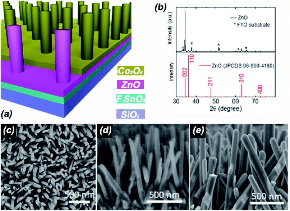 | ||
| Fig. 1 (a) The sketch of the prepared NR samples, (b) XRD pattern of the bare ZnO NRs on FTO, (c and d) HR-SEM images of the bare ZnO NRs in the plane view and lateral view, (e) HR-SEM image of the ZnO–Co3O4 heterostructure (lateral view). | ||
The AFM topography images of these ZnO NRs acquired during ImEFM measurements are shown in Fig. 2(a). The convoluted NR sizes were in the range of 100 nm to 150 nm. Taking into account the convolution of the tip and the NR diameter it could be expected that the actual NR size is less than 100 nm. These measurements are in good agreement with the SEM measurements, as shown in Fig. 1. The topographical image of the ZnO–Co3O4 junction NR acquired during the ImEFM measurements is shown in Fig. 2(b). The setpoint in the ImEFM measurements was adjusted to minimize possible cross-talk between the potential and the topography measurements. This led to a blurrier topographical image than in Fig. 2(a). The conducting AFM measurements were performed on an individual ZnO–Co3O4 NR using ImCFM. The topographies of this individual ZnO–Co3O4 NR and a NR at another larger size location are shown in Fig. 2(c) and (d). As expected, the NR diameter did not significantly increase after depositing the p-type Co3O4 film since the film thickness was only about 6–7 nm, as evaluated from the Rutherford backscattering spectroscopy (RBS) measurement. The RBS spectrum is shown in the ESI, in Fig. S1.† In addition, the stoichiometric atomic ratio of Co/O was found to be 3![[thin space (1/6-em)]](https://www.rsc.org/images/entities/char_2009.gif) :4 for the deposited cobalt oxide layer.11
:4 for the deposited cobalt oxide layer.11
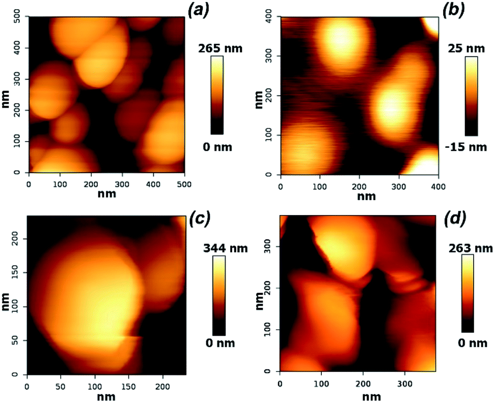 | ||
| Fig. 2 Topographical images of the grown ZnO NRs (a) and of the ZnO NRs with a p-type film of Co3O4 deposited on top of them, as measured by ImEFM (b). A topographical image of an individual ZnO–Co3O4 NR measured using ImCFM measurements in contact mode is shown in (c) Another location with ZnO–Co3O4 NRs is shown in (d). | ||
The ImEFM measurements were conducted at the setpoint, i.e. the oscillation amplitude of the AFM tip, optimized to produce good quality measurements of both the topography and contact potential difference (VCPD) distribution maps. The contact potential difference was measured for both bare ZnO NRs and the p–n junction of ZnO–Co3O4 NRs. The measured VCPD maps of the bare ZnO NRs in the dark and under light illumination are shown in Fig. 3(a) and (d). It should be mentioned that the total light illumination also includes a minor amount of light illumination at a wavelength of 900 nm from the laser driving the AFM. No clear change in the contact potential is observed for the ZnO NRs upon illumination and the difference with the measurements in the dark was found to be insignificant and less than a few mV.
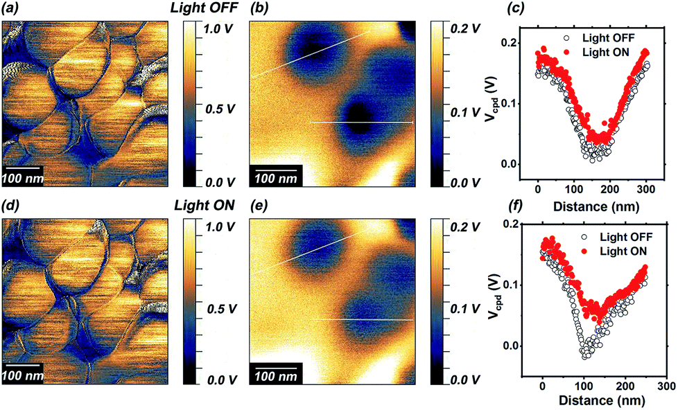 | ||
| Fig. 3 V CPD images of pure ZnO NRs measured with ImEFM in the dark (a) and under light illumination (d). VCPD images of the p–n junction NRs measured with ImEFM under no light illumination (b) and under light illumination (e). The potential distribution across the two NRs taken along the white lines shown in (b) and (e) are presented in (c) and (f), respectively. The image in (c) corresponds to the upper NR in (b). | ||
This indicates that no charge carriers are generated upon visible light illumination for the bare ZnO NRs grown on the FTO surface, as expected from the Eg of ZnO (∼3.2 eV), and sets the accuracy of a few mV to evaluate the illumination effect on the p–n NR junction. A large and clear illumination effect was observed for the ZnO–Co3O4 NRs. The difference in the measured VCPD under dark and illuminated conditions is demonstrated in Fig. 3(b) and (e).
In the measurements conducted with ImEFM the cantilever was grounded and AC voltage is applied to the substrate. The difference in the VCPD between the dark and illuminated conditions for PV materials can be regarded as the open-circuit voltage (Voc) at the nanoscale due to the addition of the quasi-Fermi level shift under illumination to the contact potential.18 Also, this difference in the VCPD between the dark and illuminated conditions can be attributed to surface photovoltage (SPV) related to the charge generation. The histogram of both VCPD images under the dark and illuminated conditions (Fig. 3(b) and (e)) was analyzed and is plotted in the ESI, Fig. S2.† A VCPD shift of about 16 mV toward higher values under light illumination is observed for entire studied area and can be explained by a change in the local electrical properties due to the generation and transport of charge carriers. Importantly, the VCPD shift for the entire image is still much larger that the change of VCPD for the pure ZnO NRs but is also smaller than the average VCPD shift of 24 mV for all NRs in Fig. 3 and smaller than the maximum VCPD changes for individual NRs studied in Fig. 3(e). It can also be concluded from the cross-section data evaluated along the NRs, Fig. 3(c) and (f), that the VCPD is moving toward higher values on top of the NRs upon illumination. This indicates that extra charge carriers, i.e. electron–hole pairs, were generated within the p–n junction NRs due to exciton creation and separation at the junction under light irradiation. The maximum difference in VCPD between dark and light conditions, which can be regarded as the ΔVoc, is about 80 mV, as evaluated from the cross-section data in Fig. 3(f). Additional VCPD measurements of the ZnO–Co3O4 NRs on a larger 1 μm by 1 μm area are provided in Fig. S3.† The evaluated maximum VCPD changes under light illumination for a few individual NRs in Fig. S3† are 42 mV and 87 mV.
These nanoscale findings are in good agreement with the microscale electrical measurements on thin film ZnO–Co3O4 photodetectors, demonstrating a Voc of about 50 mV for a 150 nm thick Co3O4 layer29 and about 150 mV for thicker Co3O4 films30 and proving its self-powering property.10 It is remarkable that for a NR architecture with a Co3O4 thickness of only 6–7 nm a similar Voc can be obtained.10 The good correlation between the macroscopically measured Voc and the nanoscale measured Voc utilizing SKPFM methods is expected and has been previously discussed.18,31 The measured values of ΔVoc are not as high as for fullerene NRs32 or a p–i–n silicon NR junction31, which are more than 500 mV, but are similar to the values obtained for some other PV materials evaluated using SKPFM methods.18,33
To summarize, the ImEFM results demonstrate a clear effect of light illumination and prove the functioning ZnO–Co3O4 NR junction. Moreover, the p–n junction NRs demonstrate varying changes in the VCPD, such as larger, smaller or very limited differences caused by light illumination, as observed in Fig. 3 and S3.† This is possibly because ZnO NRs overlap and/or there is limited electric contact of some NRs with the FTO film. Such local variation of Voc has been previously reported for different PV materials and was also related to possible microstructure and defect contributions.15,18 Also, it should be noted that various factors, such as light intensity, spectral distribution, temperature, recombination, carrier density, reverse saturation current and other contributions, can significantly affect the open-circuit voltage.17,31 This highlights how challenging NR photodetector architecture could be for nanoscale electrical measurements. On the other hand, it demonstrates the importance of such nanoscale measurements to directly probe one-dimensional nanowires and nanorods and to characterize the essential properties of such p–n junctions.
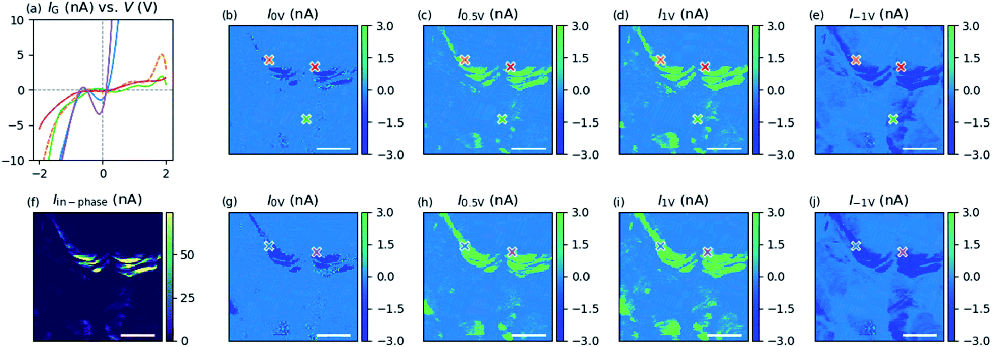
The spatially resolved I–V curves and corresponding current distribution maps at the nanometer scale under dark and illuminated conditions were measured utilizing the newly developed ImCFM method.27 ImCFM applies a full cycle of a sinusoidal oscillating voltage to every pixel of the scan. The resulting current is measured at multiple harmonics of the AC voltage to reconstruct the full I–V curve at every pixel. Representative curves are shown in Fig. 4(a). In the carried out ImCFM measurements the AC bias is applied to the cantilever and the voltage bias is applied to the sample via a conductive FTO layer below the n-type semiconductor. Thus, in the measurement system sample definition the forward bias is in the negative voltage part of the I–V curves and the reverse bias is in the positive voltage part. From the full dataset, we can then calculate the current distribution maps for any bias within the AC voltage amplitude (±1.5 V in this study). The I–V curves, demonstrating characteristic p–n junction behavior, are shown in Fig. 4(a) and 5(a). The I–V curves are taken in the dark at locations possessing no strong photocurrent generation effect (green) and photocurrent generation (orange and red). The I–V curves measured upon illumination at the same location as the orange and red marks are shown in Fig. 4(a) in blue and violet. Both areas (green; orange and red) demonstrate almost no current generation at around 0 V with an increased current generation at increasing forward and reverse biases. The current generation for the orange and red area is higher than that for the green area at increasing bias, possibly due to additional photogenerated current from the laser irradiation. This is further confirmed by the stronger current generation in this area (blue and violet) under light illumination. The maximum achieved current under light illumination is only several nA. This confirms that the generated currents in this ZnO–Co3O4 NR system are expected to be very low at the nanoscale and to be strongly affected by charge recombination.11
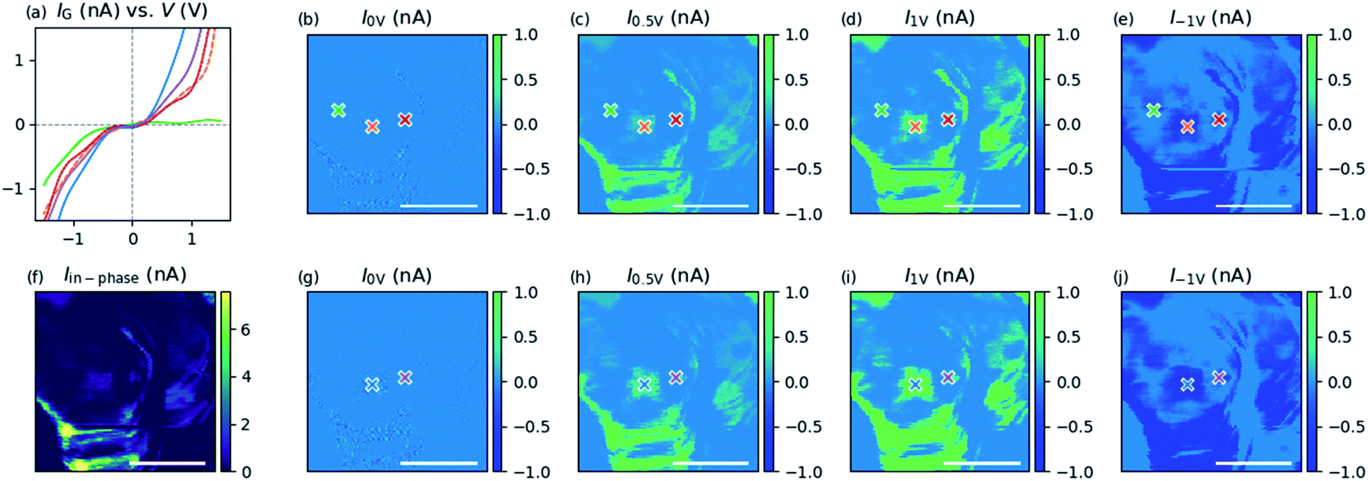 | ||
| Fig. 4 An individual p–n junction NR imaged in ImCFM mode. Current maps at 0, 0.5, 1, and −1 V bias in the dark (upper row, b, c, d and e) and under illumination (bottom row, g, h, i and j). The measured raw data (in-phase current) is shown in (f). Corresponding I–V curves taken at the green, red, orange, blue and violet marks are shown in (a). The red and orange marks show the I–V curve measured under no illumination, while the blue and violet are measured under illumination at the same location. The green mark is taken in the area without any clear illumination effect. The current scale for the maps (b–e and g–j) was set to 1 nA to highlight the small changes in the maps, while the actual measured currents were larger, as shown in the I–V curves (a). The scale bar in the image is 100 nm. | ||
 | ||
| Fig. 5 Another area measured on the NRs. Current maps measured at 0, 0.5, 1, and −1 V with ImCFM with no illumination (upper row, b, c, d and e) and under illumination (bottom row, g, h, i and j). The measured raw data (in-phase current) is shown in (f). Corresponding I–V curves taken at the green, red, orange, blue and violet marks are shown in (a). The red and orange marks show the I–V curve measured under no illumination, while the blue and violet are measured under illumination at the same location. The green mark is taken in the area without any clear illumination effect. The current scale for the maps (b–e and g–j) was set to 3 nA to highlight the small changes in the maps, while the actual measured currents were large, as shown in the I–Vcurves (a). The scale bar in the image is 100 nm. | ||
A few of these current distribution maps over an individual standing ZnO–Co3O4 NR are shown in Fig. 4, calculated at 0, 0.5, 1, and −1 V bias. The raw measured in-phase current map is shown in Fig. 4(f). The in-phase current is the real part of the current at the AC voltage frequency and provides a measure of the overall current with contributions measured at every applied voltage. Then, a current map at any applied voltage bias can easily be reconstructed from this data. The photogenerated current at short circuit, demonstrating the self-powering property for ZnO–Co3O4 NR, is expected to be seen in the 0 V current distribution map. However, this effect is not directly observed and is most likely very limited, which is in agreement with the small VCPD recorded with ImEFM. In our recent study on the self-powering effect of ZnO–Co3O4 NRs11 it was demonstrated that the magnitude of the generated photocurrent strongly depends on the thickness of the Co3O4 film. It was shown that a maximum photocurrent of tens of nA was measured for a 1 nm thick Co3O4 film with macroscopic electrical measurements providing a much larger contact area for an exposed area of 0.16 cm2. Further increasing the thickness of the p-type semiconductor to 8 nm and more significantly decreased the photogenerated current.11 Thus, the very weak photogenerated current measured in Fig. 4 at 0 V is consistent with the previously reported macroscopic observation, since the deposited p-type layer has a 6–7 nm thickness, as shown in the RBS spectrum (see Fig. S1† for details on the thickness measurements through RBS). In addition, the limited photocurrent generation at 0 V, measured with ImCFM, can be explained by the strong charge recombination, which hinders the photo induced current. Indeed, as demonstrated in ref. 11 a small applied bias of 0.1 V led to a remarkable increase of the photocurrent for the ZnO–Co3O4 NR system.
Also, the addition of a thin Al2O3 passivation layer of a few nm led to an improved photoresponse owing to the reduced recombination rate, as demonstrated in the previous study.11 The observation of the increased photogenerated current with increasing applied bias is also confirmed in the nanoscale studies utilizing ImCFM. An increase of the photogenerated current is observed with increasing voltage bias, as shown in Fig. 4(h)–(j). The current maps measured at another NR location (shown in Fig. 5) further confirm and highlight the effect of the applied bias to increase the photogenerated current, possibly due to the reduced charge recombination, as shown in Fig. 5(h)–(j). The photogenerated current has increased for both the forward and reversed biases under illumination (blue and violet I–V curves in Fig. 4 and 5) and the overall trends in the I–V curves are in good agreement with the macroscopically measured I–V curves.11 Moreover, two more distinct features are observed in Fig. 5; that there is a clear observation of a photogenerated current at 0 V under illumination, and also a presence of generated current in the dark (as is similarly observed in the ESI in Fig. S4†). The specific areas where the photogenerated current is observed demonstrate increasing current with an increase in the applied voltage. This confirms the generation of electron–hole pairs which can be locally probed with ImCFM. Also, stronger currents observed on the edges of the NRs are possibly due to the significantly increased contact area between the conducting tip and the NRs. The presence of the generated current in the dark at some of these locations can be explained by the contribution from the irradiating laser, which is well-known to contribute to such current generation, but also it can be due to the decaying contribution from a previous line scan under illumination. All of these trends in the local I–V curves observed in individual NRs, shown in Fig. 4 and 5, are in good agreement with the results from the ImCFM mapping of a larger area shown in Fig. S4.† It should also be stressed that the captured I–V curves at the nanoscale demonstrate typical behavior for a p–n junction under forward and reverse bias. A key advance of these nanoscale current ImCFM measurements over previously reported macroscale measurements is that they offer high spatial resolution and allow the visualization of various nanosize areas within a single standing NR with different electrical properties. Photogenerated currents of higher magnitude are mainly measured at the edge of NRs and in the NR center, whereas areas between the NR center and its edge do not respond to the increased bias. This is essential local information allowing the definition of where most of the charge carriers are extracted, which can lead to further improvement of NR fabrication to maximize their efficiency. Also, a tendency of a higher collection of photoinduced charges at PV NR edges is known and has been demonstrated for μ-cell and PV thin film grain boundaries.16,34 The important advantage of the ImCFM method over standard CAFM and pcAFM is that every pixel in the current distribution maps already contains current–voltage curves, and map data capturing is very fast. The measured current magnitude at increasing bias is similar to some other PV systems studied with CAFM methods.27,32,33,35 The ImCFM studies have revealed the nanoscale photocurrent distribution in a novel standing ZnO–Co3O4 NR photodetector.
Conclusions
To summarize, new methods in dynamic multifrequency AFM, such as ImEFM and ImCFM, were applied to elucidate the nanoscale electrical properties of novel ZnO–Co3O4 NR heterojunctions, which were able to operate as photodetectors. Both techniques provided high current and potential nanoscale spatial resolution with significantly improved scanning times, in the case of ImCFM. Unique current distribution maps offering captured I–V curves for every image pixel were obtained with ImCFM. The effect of light illumination on the electric properties and photocurrent generation in a single ZnO–Co3O4 NR was observed and quantified. No clear photoinduced current was observed at 0 V bias on an individual NR due to fast charge recombination occurring, as previously reported in macroscale electrical measurements for this system.11 A slight increase in both the applied forward and reverse bias voltages facilitated an increased photogenerated current. However, weak photogenerated currents in the magnitude of several nA were measured on some NR edges at 0 V bias, probably due to the significantly increased contact area between the tip and the NRs. Importantly, the photogenerated currents at 0 V applied bias in such areas were further increased upon increasing the applied bias. The ImCFM method also allowed us to measure and visualize nanoscale areas within a single NR with high and low generated photocurrents. This demonstrates that even a single NR undergoes heterogeneous photocurrent generation related to its local surface structure. These findings provide essential results for the future development of all-oxide ZnO–Co3O4 NR photodetectors and PV devices to maximize their efficiency. In a broader perspective, such nanoscale results at a high spatial resolution can support the structure–functionality relationship in optically active heterostructured nanomaterials and nanojunctions (including non-planar structures).Experimental
Materials
Zinc acetate dihydrate (Zn(CH3COO)2·2H2O), zinc nitrate hexahydrate (Zn(NO3)2·6H2O) and hexamethylenetetramine (HMT) were purchased from Sigma-Aldrich. Cobalt alkyl amidinate was purchased from Strem Chemicals. Deionized water was used in atomic layer deposition (ALD) using a Savannah 200 system. Ethanol (99.9%) and distilled water were used in all processes.A detailed procedure for the NR synthesis and photodetector preparation can be found in our previous publication.11
A brief description of the process is as follows:
Synthesis of the ZnO–Co3O4 NRs
A ZnO seed layer was prepared by the spin coating of 0.1 M of zinc acetate solution in ethanol at 3000 rpm for 30 s. The sample was further annealed at 450 °C for 1 hour in a furnace. ZnO NRs were prepared by hydrothermal synthesis. A solution of a mixture of 100 mM zinc nitrate and 100 mM HMT in distilled water was prepared for growing the ZnO NRs. The Co3O4 thin film was deposited by means of ALD. The cobalt source was heated up to 110 °C and DI water as the oxidation source was used at room temperature.Preparation of the photodetector
To prepare the NR device, fluorine-doped tin oxide (FTO) conducting glass (Pilkington TEC 15, 15 Ω sq−1) was used as the substrate. The substrate was precleaned in distilled water and ethanol using 15 minutes of sonication in each medium. Then, the seed layer solution was deposited on the FTO conductive glass using spin coating, followed by an annealing process. The seeded FTO sample was placed in a hydrothermal autoclave containing the hydrothermal solution. The autoclave was heated to 95 °C for 6 hours. The substrate was then rinsed with distilled water and placed in the ALD reaction chamber at 200 °C for Co3O4 deposition.Methods
X-ray diffraction data were gathered using a PANalytical Empyrean instrument operating in Bragg Brentano geometry with a Cu tube at 45 kV and 40 mA.Rutherford backscattering spectroscopy (RBS) with a 2.0 MeV 4He+ beam in IBM geometry at a scattering angle of θ = 160° was used to measure the Co3O4 layer thickness after deposition.
The high-resolution (HR) scanning electron microscopy was carried out with a field emission SEM Magellan 400 instrument (FEI Company).
The ImEFM measurements were conducted using a NanoWizard ULTRA Speed AFM (JPK Instruments AG) mounted on an inverted optical microscope (Nikon Corporation). A multi-frequency lock-in amplifier (MLA) (Intermodulation Products AB) was connected to the JPK NanoWizard AFM. The VCPD measurements were carried out at ambient conditions in air using HQ:NSC15 probes (MikroMasch) with platinum coating. The nominal tip outer radius is less than 30 nm and the nominal cantilever spring constant is 40 N m−1. The possible cross-talk between the measured topography and the surface potential measurement was minimized by optimized the imaging setpoint, i.e. by adjusting the tip–surface interaction force. The acquisition speed for ImEFM measurements was 1 line per second, the images contain 256 × 256 data points and the surface potentials were not inverted. An AC bias of 6 V was applied to the tip for the measurements. The setpoint was 88% and the driving amplitude was 100 nm for the measurements on pure ZnO. The setpoint was 80% and the driving amplitude was 200 nm for the measurements on ZnO–Co3O4 NR. The calibrated resonance frequencies typically were 262.5 kHz (for ZnO–Co3O4 measurements) and 295 kHz (for ZnO measurements).
The ImCFM measurements were conducted using a NanoWizard ULTRA Speed AFM (JPK Instruments AG) equipped with the same MLA. The tip current was converted to voltage using a DLPCA-200 variable-gain and a low-noise current amplifier (FEMTO Messtechnik GmbH). The voltage was then sampled by the MLA. A more detailed procedure is described in the method introduction paper.27 A separation frequency, df, of 100 Hz was used during the scanning. The contact mode imaging was run at a deflection signal to set point signal difference of 0.2 to 0.3 V.
The samples were illuminated through the microscope objective which focused the light from a white light-emitting diode (Sloan AG, Basel), with a maximum emission intensity at a wavelength of around 470 nm, onto the scanned area. The light illumination was alternately switched on and off during the scanning trace and retrace (approximately 1 Hz) to compare the electrical response of the photodetector upon conditions of illumination and no illumination. RMN-12PT400B probes (Bruker), with a nominal spring constant of 0.3 N m−1 and an outer tip radius of about 20 nm, were utilized for the ImCFM measurements.
The data were analyzed using the IMP software suite (version 1.1, Intermodulation Products AB) and the SPM images were prepared using Gwyddion software (version 2.44).
Conflicts of interest
RB is a part owner of Intermodulation Products AB, which manufactures and sells the multifrequency lock-in amplifier used in this study.Acknowledgements
The authors acknowledge the Kempe Foundations and the Knut & Alice Wallenberg Foundation for the financial support.Notes and references
- W. Tian, Y. Wang, L. Chen and L. Li, Small, 2017, 13, 1701848 Search PubMed.
- S. Rühle, A. Y. Anderson, H.-N. Barad, B. Kupfer, Y. Bouhadana, E. Rosh-Hodesh and A. Zaban, J. Phys. Chem. Lett., 2012, 3, 3755–3764 Search PubMed.
- A. Vomiero, I. Concina, E. Comini, C. Soldano, M. Ferroni, G. Faglia and G. Sberveglieri, Nano Energy, 2012, 1, 372–390 Search PubMed.
- H. Lu, W. Tian, F. Cao, Y. Ma, B. Gu and L. Li, Adv. Funct. Mater., 2016, 26, 1296–1302 Search PubMed.
- I. Concina, Z. H. Ibupoto and A. Vomiero, Adv. Energy Mater., 2017, 7, 1700706 Search PubMed.
- W. Ouyang, F. Teng, J.-H. He and X. Fang, Adv. Funct. Mater., 2019, 29, 1807672 Search PubMed.
- D. S. Wiersma, P. Bartolini, A. Lagendijk and R. Righini, Nature, 1997, 390, 671–673 Search PubMed.
- B. D. Yuhas and P. Yang, J. Am. Chem. Soc., 2009, 131, 3756–3761 Search PubMed.
- P. Krogstrup, H. I. Jørgensen, M. Heiss, O. Demichel, J. V. Holm, M. Aagesen, J. Nygard and A. Fontcuberta i Morral, Nat. Photonics, 2013, 7, 306–310 Search PubMed.
- P. Ghamgosar, F. Rigoni, S. You, I. Dobryden, M. G. Kohan, A. L. Pellegrino, I. Concina, N. Almqvist, G. Malandrino and A. Vomiero, Nano Energy, 2018, 51, 308–316 Search PubMed.
- P. Ghamgosar, F. Rigoni, M. G. Kohan, S. You, E. A. Morales, R. Mazzaro, V. Morandi, N. Almqvist, I. Concina and A. Vomiero, ACS Appl. Mater. Interfaces, 2019, 11, 23454–23462 Search PubMed.
- K. Zhang, Z. L. Wang and Y. Yang, ACS Nano, 2016, 10, 10331–10338 Search PubMed.
- E. M. Tennyson, J. M. Howard and M. S. Leite, ACS Energy Lett., 2017, 2, 1825–1834 Search PubMed.
- J. L. Garrett, M. S. Leite and J. N. Munday, ACS Appl. Mater. Interfaces, 2018, 10, 28850–28859 Search PubMed.
- E. M. Tennyson, C. Gong and M. S. Leite, ACS Energy Lett., 2017, 2, 2761–2777 Search PubMed.
- Y. Kutes, B. A. Aguirre, J. L. Bosse, J. L. Cruz-Campa, D. Zubia and B. D. Huey, Progr. Photovolt.: Res. Appl., 2016, 24, 315–325 Search PubMed.
- N. K. Elumalai and A. Uddin, Energy Environ. Sci., 2016, 9, 391–410 Search PubMed.
- E. M. Tennyson, J. L. Garrett, J. A. Frantz, J. D. Myers, R. Y. Bekele, J. S. Sanghera, J. N. Munday and M. S. Leite, Adv. Energy Mater., 2015, 5, 1501142 Search PubMed.
- R. Kumar, D. Varandani and B. R. Mehta, Carbon, 2016, 98, 41–49 Search PubMed.
- C. de Melo, M. Jullien, Y. Battie, A. En Naciri, J. Ghanbaja, F. Montaigne, J.-F. Pierson, F. Rigoni, N. Almqvist, A. Vomiero, S. Migot, F. Mücklich and D. Horwat, ACS Appl. Mater. Interfaces, 2018, 10, 40958–40965 Search PubMed.
- C. de Melo, M. Jullien, J. Ghanbaja, F. Montaigne, J.-F. Pierson, F. Soldera, F. Rigoni, N. Almqvist, A. Vomiero, F. Mücklich and D. Horwat, ACS Appl. Mater. Interfaces, 2018, 10, 37671–37678 Search PubMed.
- J. Luria, Y. Kutes, A. Moore, L. Zhang, E. A. Stach and B. D. Huey, Nat. Energy, 2016, 1, 16150 Search PubMed.
- R. Garcia and E. T. Herruzo, Nat. Nanotechnol., 2012, 7, 217–226 Search PubMed.
- D. Platz, E. A. Tholén, D. Pesen and D. B. Haviland, Appl. Phys. Lett., 2008, 92, 153106 Search PubMed.
- D. Forchheimer, R. Forchheimer and D. B. Haviland, Nat. Commun., 2015, 6, 6270 Search PubMed.
- R. Borgani, D. Forchheimer, J. Bergqvist, P.-A. Thorén, O. Inganäs and D. B. Haviland, Appl. Phys. Lett., 2014, 105, 143113 Search PubMed.
- R. Borgani, M. Gilzad Kohan, A. Vomiero and D. B. Haviland, Phys. Rev. Appl., 2019, 11, 44062 Search PubMed.
- C. Musumeci, R. Borgani, J. Bergqvist, O. Inganäs and D. Haviland, RSC Adv., 2017, 7, 46313–46320 Search PubMed.
- M. Patel, M. Kumar, H.-S. Kim, W.-H. Park, E. H. Choi and J. Kim, Mater. Sci. Semicond. Process., 2018, 74, 74–79 Search PubMed.
- A. K. Rana, M. Patel, T. T. Nguyen, J.-H. Yun and J. Kim, Mater. Sci. Semicond. Process., 2020, 117, 105192 Search PubMed.
- C. Marchat, L. Dai, J. Alvarez, S. Le Gall, J.-P. Kleider, S. Misra and P. Roca i Cabarrocas, Nanoscale Res. Lett., 2019, 14, 398 Search PubMed.
- W. C. Tsoi, P. G. Nicholson, J. S. Kim, D. Roy, T. L. Burnett, C. E. Murphy, J. Nelson, D. D. C. Bradley, J.-S. Kim and F. A. Castro, Energy Environ. Sci., 2011, 4, 3646–3651 Search PubMed.
- J. Rahova, K. Sampathkumar, A. Vetushka, M. Ledinsky, Z. Hajkova, A. Fejfar and O. Frank, Phys. Status Solidi B, 2018, 255, 1800305 Search PubMed.
- N. Muhunthan, O. P. Singh, V. Toutam and V. N. Singh, Mater. Res. Bull., 2015, 70, 373–378 Search PubMed.
- J. Hieulle, C. Stecker, R. Ohmann, L. K. Ono and Y. Qi, Small Methods, 2018, 2, 1700295 Search PubMed.
Footnote |
| † Electronic supplementary information (ESI) available. See DOI: 10.1039/d1na00319d |
| This journal is © The Royal Society of Chemistry 2021 |