
 Open Access Article
 This Open Access Article is licensed under a Creative Commons Attribution-Non Commercial 3.0 Unported Licence
MoS2 nanoparticle/activated carbon composite as a dual-band material for absorbing microwaves†
Praveen
Negi
and
Ashavani
Kumar
 *
*
Department of Physics, National Institute of Technology Kurukshetra, Haryana 136119, India. E-mail: ashavani@yahoo.com; ashavani@nitkkr.ac.in
First published on 24th May 2021
Abstract
In the search for novel high-performance microwave (MW) absorbers, MoS2 has shown promise as a MW-absorbing material, but its poor impedance matching limits its applications. Herein, a facile hydrothermal method was used to produce a composite consisting of activated carbon (AC) derived from waste biomass and in situ-grown MoS2 nanoparticles. Its microwave absorption properties were examined in the 2–18 GHz frequency range, and FESEM and HRTEM images confirmed the formation of MoS2 nanoparticles on the AC. The maximum reflection loss (RLmax) for the MoS2/AC composite was −31.8 dB (@16.72 GHz) at 20 wt% filler loading. At 50 wt% filler loading, the MoS2/AC (MAC50) composite exhibited unique dual-band absorption characteristics in the C and Ku bands. An effective absorption bandwidth (RL < −10 dB) of 10.4 GHz (3–5.2 GHz, 9.8–18 GHz) was achieved at various thicknesses that covered the entire Ku band. Therefore, a sole dielectric absorber can easily be tuned to absorb MWs at multiple frequency ranges. The large surface area and conduction losses of AC combined with the superior dielectric loss properties of MoS2 resulted in improved impedance matching and attenuation ability of the MoS2/AC composite. Thus, MoS2/AC is a promising low-cost dielectric absorber for MW absorption applications.
1. Introduction
In the past decade, there has been a rapid surge in modern technology, especially in the fields of electronics and wireless communications. This has led to wide interest in developing novel microwave (MW)-absorbing materials. A high-performance MW absorber should strongly absorb with a wide effective absorption bandwidth (EAB), i.e., the frequency range where reflection loss (RL) <−10 dB, and should also be lightweight, with good thermal stability, and the ability to tune MW absorption to desired frequency bands.1,2A two-dimensional (2D) transition metal dichalcogenide, molybdenum disulphide (MoS2), has shown promise as a microwave-absorbing material in recent years due to its large specific surface area and high dielectric properties.1–4 Ning et al.5 prepared 2D MoS2 nanosheets using a top-down exfoliation method and reported a maximum reflection loss (RLmax) = −38.42 dB. Liang et al.6 used a hydrothermal process to fabricate MoS2 nanosheets and obtained an RLmax value of −47.8 dB. To enhance the MW absorption properties of MoS2, there are generally two approaches: first, to combine a magnetic material with MoS2 such as MoS2/FeS2,7 MoS2–iron oxide,3 porous coin-like Fe@MoS2,8 or BaFe12O19@MoS2,9 and second, to incorporate a nonmagnetic or pure dielectric material with MoS2.
A pure dielectric absorber faces the problem of poor impedance matching,2 but in recently reported studies, it was demonstrated that when various carbon-based materials were combined with MoS2, the MW absorption by a dielectric absorber was enhanced. An excellent EAB of 10.85 GHz was measured for the MoS2-coated carbon fiber fabricated by Zhang et al.10 The MoS2/carbon nanotube (CNT) (2D/1D) composite synthesized by Sun et al. gave a maximum EAB = 5.60 GHz (RLmax = −47.9 dB).11 The MoS2 nanosheet/3D carbon foam reported by Lyu et al.12 yielded a RLmax = −45.88 dB and EAB = 5.68 GHz, and the MoS2/reduced graphene oxide (RGO) hybrid prepared by Wang et al. achieved a RLmax = −50.9 dB and EAB of 5.72 GHz.13 The EAB values of 5.92 GHz,14 6.96 GHz,15 and 5.6 GHz (ref. 16) reported by other research groups confirm the enhanced MW absorption performance for the MoS2/RGO composite.
Another carbon-based MoS2 composite, i.e., carbon spheres, has also been used to achieve superior MW-absorbing properties. The core–shell carbon-sphere CS/MoS2 composite fabricated by Zhang et al.4 provided a RLmax = −52.6 dB (EAB = 6.29 GHz), whereas Ning et al.2 encapsulated MoS2 nanosheets in hollow carbon spheres and obtained an excellent RLmax = −65 dB. The morphologically based study performed by Zhang et al.17 also concluded that a MoS2/carbon composite with a microsphere morphology provided a more optimal MW-absorbing performance than pure MoS2. The incorporation of carbon-based materials with MoS2 provides multiple interfaces that increase interfacial polarization14,17 and facilitate the multiple reflections of incident MWs.3,4 It also improves impedance matching of the composite and thus reduces surface reflections.2
Recently, biomass-based activated carbon has emerged as a potential dielectric loss material for MW-absorbing applications.18–23 The presence of natural and artificial porosity in the activated carbon facilitates multiple reflections and scattering of incident MWs.21,22 Our group has also reported that mango leaf-based activated carbon is an excellent MW-absorbing material.24 Therefore, due to its remarkable properties such as large surface area, adequate porosity, light weight, sustainable natural source, and low cost,21,23 an activated carbon-based dielectric composite is a potential candidate for MW absorption applications.
In the present study, a MoS2/activated carbon composite was synthesized, and its MW absorption properties were reported. The composite at 20 wt% filler loading yielded an RLmax = −31.8 dB at 16.72 GHz, whereas at 50 wt% filler loading, the absorber gave a dual-band RL in the C and Ku bands. The dual-band MW-absorption performances reported by Liu et al.25 and Shu et al.26 used co-doped NiZn ferrite/graphene and RGO/MWCNTs/ZnFe2O4 nanocomposites, respectively. These composites were constructed from dielectric and magnetic materials, whereas Zhang et al.1 reported a solely dielectric-based VS2 nanosheet that exhibited dual-band MW absorption in the C and Ku bands. Thus, the dual-band loss shown by the MoS2/activated carbon (AC) composite is unique and, to the best of our knowledge, has not been reported for any MoS2/carbon-based composites.
2. Experimental
2.1. Materials
Sodium molybdate dihydrate (Na2MoO4·2H2O) ACS grade and potassium hydroxide (KOH) AR grade were purchased from Merck Life Science Pvt. Ltd. L-Cysteine, paraffin wax, and hydrochloric acid (HCl) were purchased from Lobachemie Pvt. Ltd. Ethanol was purchased from Changshu Pvt. Ltd., and mango leaves were collected on the Institute premises.2.2. Synthesis of the MoS2/AC composite
Waste mango leaf-based AC was synthesized by a facile method of carbonization followed by its activation using KOH, as previously reported by our group.24 The MoS2/AC composite was prepared by a hydrothermal method. Sodium molybdate and L-cysteine (1![[thin space (1/6-em)]](https://www.rsc.org/images/entities/char_2009.gif) :5 molar ratio) were dissolved in 30 ml of deionized (DI) water. After the AC in DI water was sonicated for 1 hour, both solutions were mixed and then stirred for 2 hours to form a uniform solution. The ratio of MoS2 to AC was maintained at 1:0.5. The pH was decreased to approximately 2 by adding HCl to the solution. The 80 ml solution of sodium molybdate, L-cysteine, and AC was then transferred to a Teflon-lined stainless-steel autoclave (100 ml) and heated at 180 °C for 24 h. The as-prepared precipitate was then washed with DI water and ethanol using a centrifuge until a neutral pH was achieved. The washed sample was then dried in an oven at 100 °C overnight. The resulting MoS2/AC composite was named MAC, and an illustration of the preparation of the MoS2/AC composite is shown in Scheme 1.
:5 molar ratio) were dissolved in 30 ml of deionized (DI) water. After the AC in DI water was sonicated for 1 hour, both solutions were mixed and then stirred for 2 hours to form a uniform solution. The ratio of MoS2 to AC was maintained at 1:0.5. The pH was decreased to approximately 2 by adding HCl to the solution. The 80 ml solution of sodium molybdate, L-cysteine, and AC was then transferred to a Teflon-lined stainless-steel autoclave (100 ml) and heated at 180 °C for 24 h. The as-prepared precipitate was then washed with DI water and ethanol using a centrifuge until a neutral pH was achieved. The washed sample was then dried in an oven at 100 °C overnight. The resulting MoS2/AC composite was named MAC, and an illustration of the preparation of the MoS2/AC composite is shown in Scheme 1.
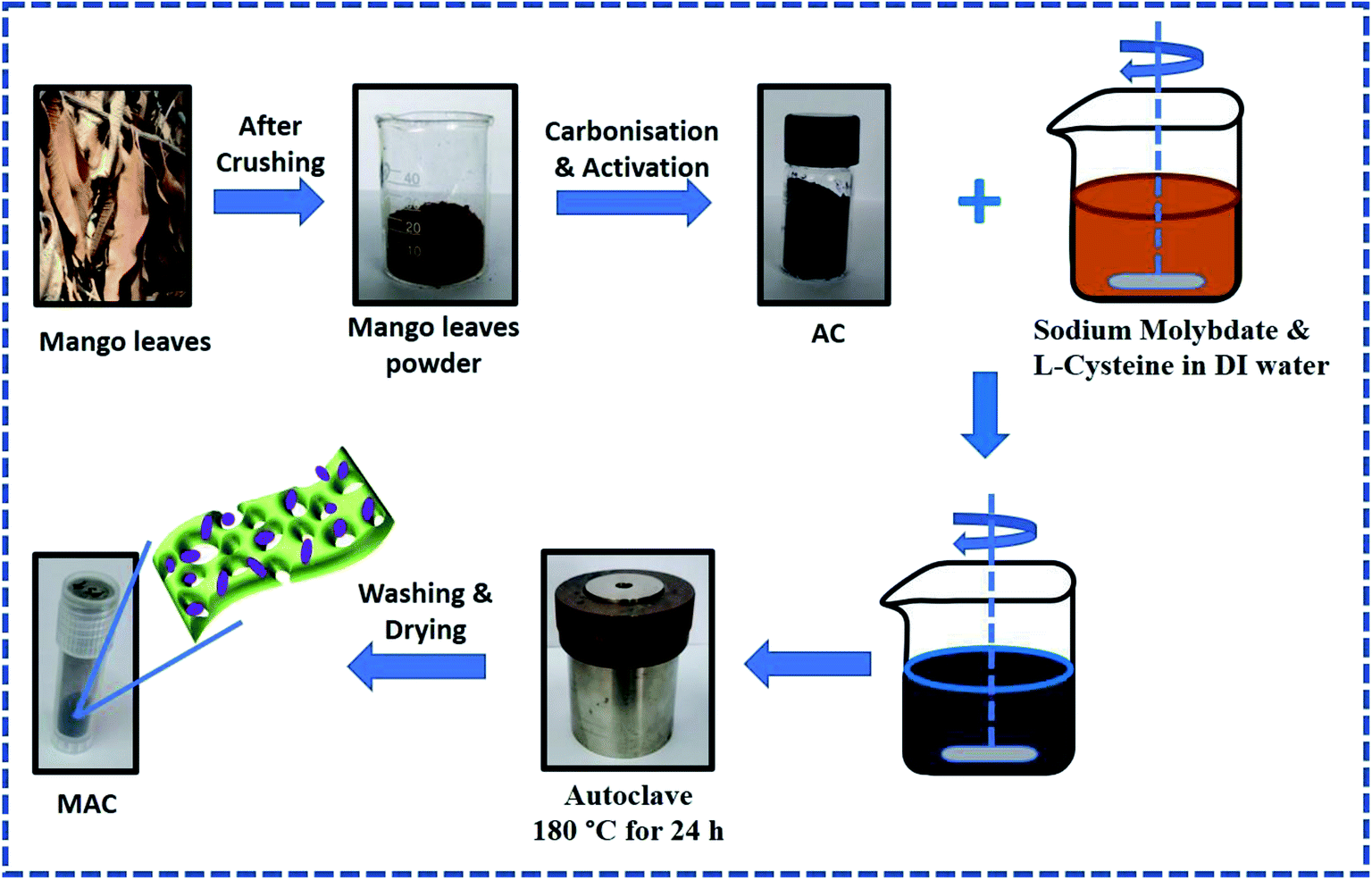 | ||
| Scheme 1 Schematic illustration for the preparation of the MoS2/AC composite. | ||
2.3. Characterization
Powder X-ray diffraction (XRD) was performed using a Rigaku Miniflex II with Cu Kα radiation (λ = 1.54 Å). A confocal micro-Raman spectrometer (AIRIX CORP) with laser excitation at 532 nm was used to obtain Raman spectra. The morphology was studied by field emission scanning electron microscopy (FESEM, FEI Nova Nano) and high-resolution transmission electron microscopy (HRTEM, FEI Tecnai G2 20 S-TWIN). A Thermo Fisher Scientific Nexsa base was used to record X-ray photoelectron spectra (XPS). A Quantachrome Nova 2200e was used to measure nitrogen adsorption–desorption isotherms at 77.3 K. A multiple points Brunauer–Emmett–Teller (BET) method was used to calculate the specific surface area, and the Barrett, Joyner, and Halenda (BJH) model was used to calculate the pore size distribution.2.4. Microwave absorption measurements
To study the microwave absorption properties, MAC powder and paraffin wax were mixed and heated at 100 °C. The mixture was then pressed into a toroidal shape (φout = 7.0 mm, φin = 3.0 mm) using a die. The wt% of MAC in wax was varied, and 10%, 20%, 30%, 40%, and 50% were tested. Therefore, the samples were named MAC10, MAC20, MAC30, MAC40, and MAC50, where the numbers represent the loading wt% of MAC in paraffin wax.An Agilent E8364B PNA series vector network analyzer (VNA) was used to obtain the relative complex permittivity (εr) and permeability (μr) in the frequency range of 2–18 GHz. The RL values were calculated by the following eqn (1) and (2):2,14
| RL (dB) = 20log|(Zin − Z0)/(Zin + Z0)| | (1) |
 | (2) |
3. Results and discussion
3.1. Morphological and structural analyses
Fig. 1a depicts the XRD pattern of AC where the broad peak at 2θ = 23.6° corresponds to the (002) plane and a weak peak at 2θ = 43.2° corresponds to the (100) plane. These two planes confirm the graphitic nature of AC.18,24,27 These broad and weak peaks of AC indicate the low level of crystallinity and amorphous nature of porous AC.18 The XRD pattern of the MoS2/AC composite as shown in Fig. 1b contains characteristic diffraction peaks at 2θ = 14.3°, 32.6°, and 58.2° that correspond to the (002), (100), and (110) planes of MoS2, respectively (JCPDS card no. 37-1492).2,4,15 The broadening of peaks implies the formation of nano-sized MoS2 particles28 that were further confirmed by FESEM and HRTEM images. The intensity of the (002) plane of AC in the MoS2/AC composite was suppressed, and this can be attributed to the formation of MoS2 nanoparticles on the surface of carbon sheets as well as the low crystallinity of AC.13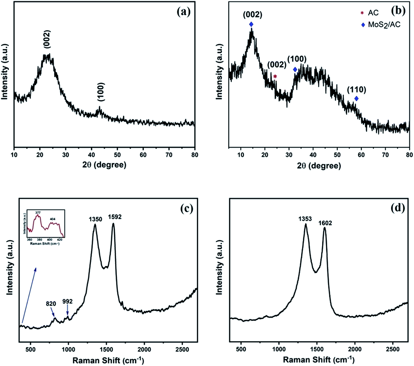 | ||
| Fig. 1 XRD pattern of (a) activated carbon (AC) and (b) MoS2/AC composite (MAC), and Raman spectrum of (c) MAC and (d) AC. | ||
The nitrogen adsorption–desorption isotherm as depicted in Fig. S1† was obtained to study the porosity of AC. The activation process by KOH resulted in a large specific surface area (SBET = 995.129 m2 g−1). The BJH pore size distribution (Fig. S1† inset) revealed that the total pore volume was 0.513 cm3 g−1, and the majority of pore sizes were in the range of 2–26 nm, which indicates the presence of mesopores in the AC.29 The presence of AC in the MoS2/AC composite was further confirmed by Raman analysis, as shown in Fig. 1c. The two strong peaks present at 1350 cm−1 (D band) and 1592 cm−1 (G band) are characteristic of graphitic carbon.3,24 The G band arose due to the E2g vibrational mode present within the aromatic carbon rings,30 and it also represents the degree of graphitization.31 The D band is attributed to the defects and disorder introduced into sp2 carbon.27,31,32
When compared with the Raman spectra of AC (Fig. 1d), which exhibited a D band at 1353 cm−1 and G band at 1602 cm−1, a blueshift was observed for the MAC Raman spectra, which can be attributed to the stress induced in AC by the formation of MoS2 nanoparticles.33 The two weak peaks at 377 cm−1 and 404 cm−1 shown in the Fig. 1c inset are the first-order Raman modes present in MoS2, and these modes are associated with in-plane vibration (E12g) and out-of-plane vibration (A1g), respectively.2,13,34 The other minor peaks at approximately 820 cm−1 and 992 cm−1 are attributed to the partial oxidation of MoS2 (ref. 34 and 35) by the laser power used in Raman spectroscopy.36
The FESEM images shown in Fig. 2(a–d) depict the distribution of MoS2 particles over the AC. The voids and pores formed in the carbon structure due to the activation process serve as a nucleation site for MoS2 nanoparticles, hence the nanoparticles are also visible inside the pores (Fig. 2(c and d)). The majority of nanoparticles are in the range of 60 to 80 nm, as depicted in the particle size distribution graph of MoS2 nanoparticles (Fig. S2†). The TEM images clearly depict the AC sheets (Fig. 2e), as well as the formation of the nano-sized MoS2 particles (Fig. 2f). The HRTEM image depicted in Fig. 2g shows interlayer spacing of 0.27 nm that corresponds to the (100) plane of MoS2,37,38 whereas the selected area electron diffraction (SAED) pattern given in Fig. 2h resulted from the (100) and (110) planes of MoS2.13,16
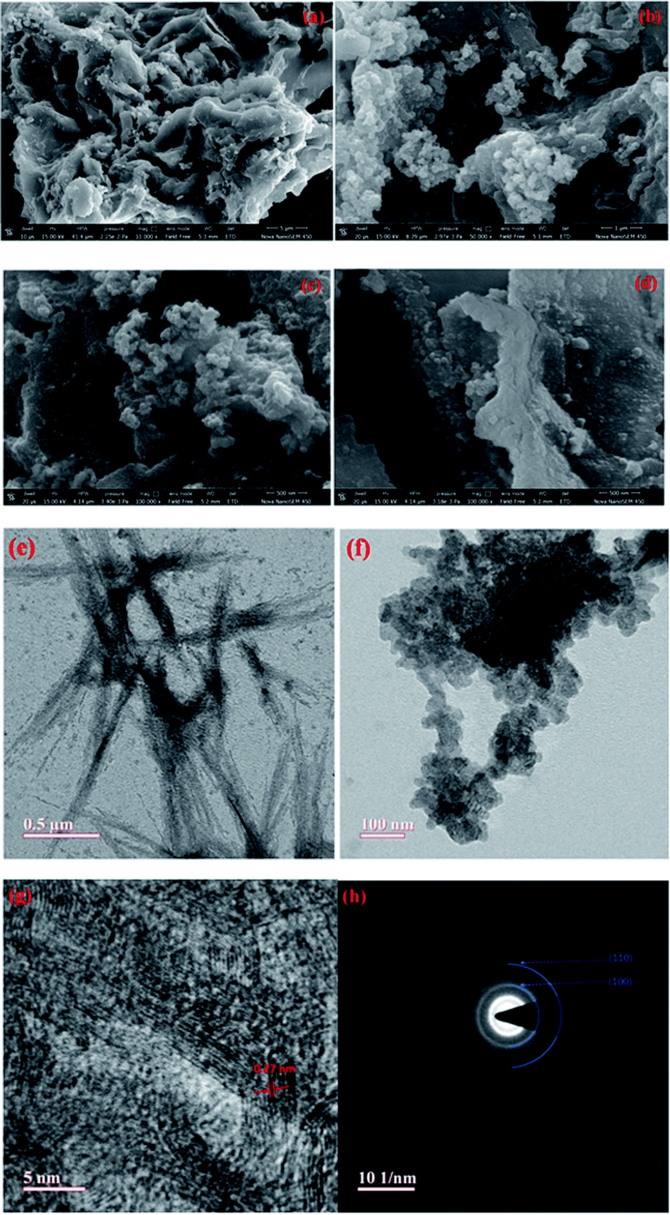 | ||
| Fig. 2 (a–d) FESEM images, (e, f) TEM images, (g) HRTEM image, and (h) SAED pattern of MAC. | ||
X-ray photoelectron spectroscopy (XPS) was performed to analyze the chemical composition and oxidation states of the elements present in the MoS2/AC composite. Fig. 3a shows the full XPS spectrum of the composite, which confirms the presence of Mo, S, C, and O elements.14,39,40 The atomic percents of Mo, S, and C were 12.64%, 26.73%, and 22.16%, respectively. The atomic ratio of Mo and S is 1:2.1, which is very close to the theoretical value of MoS2, whereas the atomic ratio of MoS2 and carbon is approximately 1:0.56, which is quite close to the initial precursor values. Fig. 3b depicts the high-resolution spectrum of Mo 3d, in which the Mo 3d5/2 and Mo 3d3/2 orbitals at approximately 229.5 eV and 232.7 eV, respectively, determine the existence of Mo4+.2,3,15Fig. 3c shows the high-resolution spectra of C 1s, which was de-convoluted into three peaks. The most dominating peak at approximately 285 eV corresponds to the C–C/C![[double bond, length as m-dash]](https://www.rsc.org/images/entities/char_e001.gif) C group, while the minor peaks at approximately 286.5 eV and 288.3 eV correspond to the C–O and CO groups, respectively.2,3,15 The S 2p high-resolution spectrum depicted in Fig. 3d was de-convoluted into three peaks. The peaks at approximately 162.5 eV and 163.7 eV correspond to the 2p3/2 and 2p1/2 orbitals40,41 respectively, whereas the peak at approximately 164.9 eV corresponds to the C–S–C group.39,42,43
C group, while the minor peaks at approximately 286.5 eV and 288.3 eV correspond to the C–O and CO groups, respectively.2,3,15 The S 2p high-resolution spectrum depicted in Fig. 3d was de-convoluted into three peaks. The peaks at approximately 162.5 eV and 163.7 eV correspond to the 2p3/2 and 2p1/2 orbitals40,41 respectively, whereas the peak at approximately 164.9 eV corresponds to the C–S–C group.39,42,43
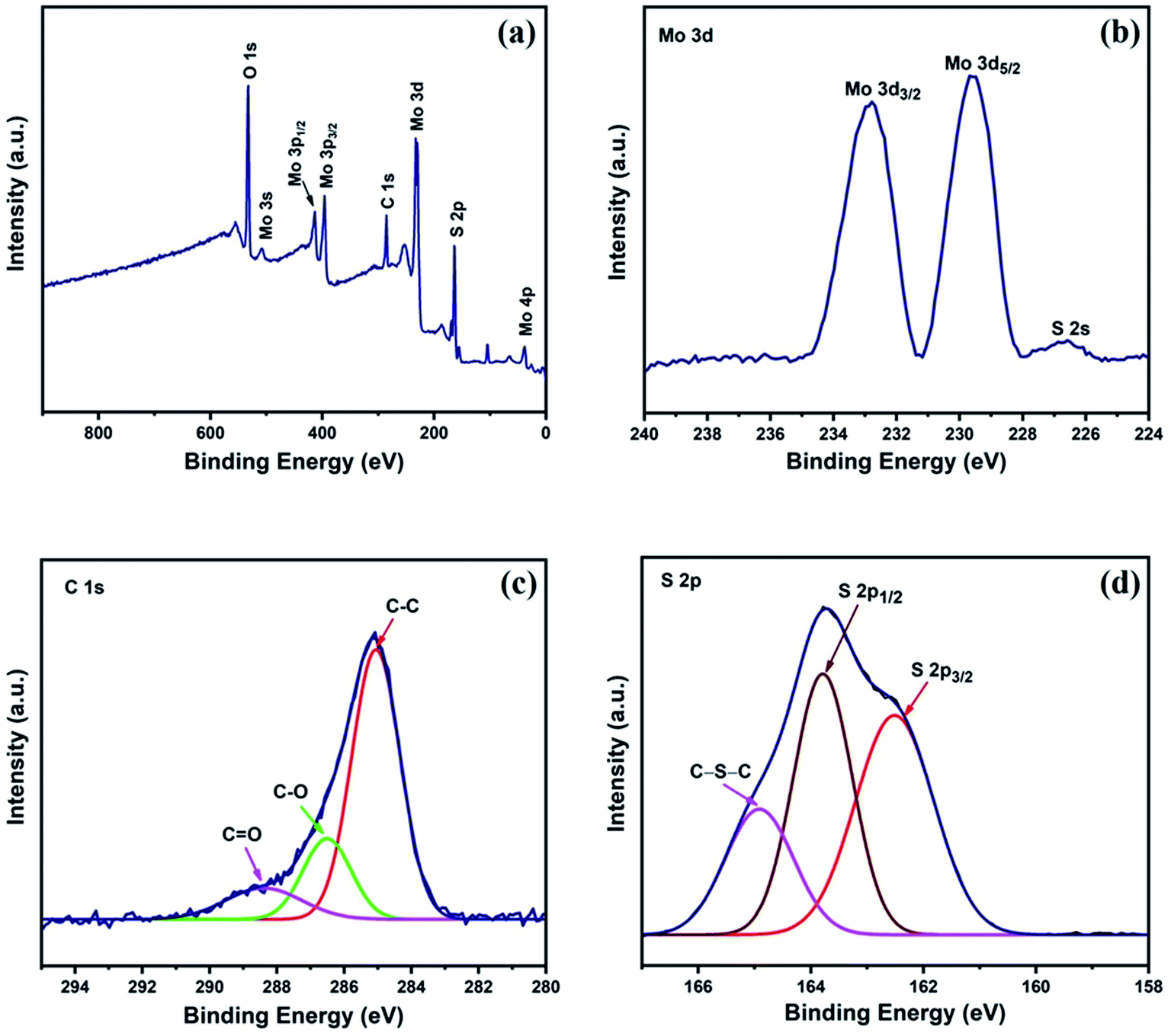 | ||
| Fig. 3 (a) XPS survey spectra and high resolution spectra of (b) Mo 3d, (c) C 1s, and (d) S 2p for MAC. | ||
3.2. Microwave absorption properties
To study the microwave absorption properties of an absorber, the two important parameters, i.e., εr and μr were obtained from VNA. Because both MoS2 and AC are nonmagnetic materials, hence the value of μr was taken to be 1. The εr consists of two parts: the real part of permittivity (ε′) represents the storage of energy, whereas the imaginary part of permittivity (ε′′) represents the energy dissipation.4The value of ε′ for all the samples shows a decreasing trend with increase in frequency, with minor fluctuations as shown in Fig. 4a. The ε′ value for MAC10, MAC20, MAC30, MAC40, and MAC50 are in the range of 2.69–2.57, 3.95–3.49, 5.19–4.54, 7.58–6.33, and 11.68–9.08, respectively. The value of ε′ increases with increasing concentration of MAC in paraffin wax, as per effective medium theory,2,4,15 and the increase in MAC in paraffin wax leads to an increase in interfacial polarization. Multiple interfaces within the paraffin matrix are created by the porous structure of AC along with the MoS2 nanoparticles, which amplifies the interfacial polarization. Hence, there will be clear increases in the values of ε′ with increasing filler (MAC) loading.
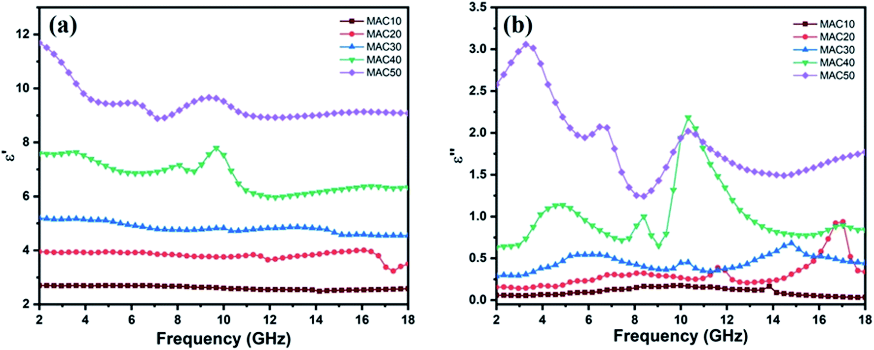 | ||
| Fig. 4 (a) The real part and (b) imaginary part of the relative complex permittivity of the MAC–paraffin wax composite with different filler loadings ranging from 10 wt% to 50 wt%. | ||
Similar to ε′, the ε′′ values as depicted in Fig. 4b also show an increasing trend with increasing filler (MAC) loading. This can be attributed to the increase in the AC content, which increases the electrical conductivity of sample. According to free electron theory: ε′′ ≈ 1/(2πε0fρ)−1,3,44 where ρ denotes the resistivity of an absorber, ε0 denotes the permittivity of free space, and f denotes the electromagnetic (EM) wave frequency. Therefore, increasing the carbon content decreases the electrical resistivity of the absorber, which increases the ε′′ value. As the MAC loading increased above 10 wt%, several relaxation peaks were obtained in the complex permittivity.5 Fig. S3(a–d)† shows two peaks for MAC20 and MAC30, whereas there are 3 peaks for MAC40 and MAC50. The peak in the frequency range of 10–12 GHz is common in all the graphs, which suggests that the complex permittivity of the MAC–wax composite has a resonant characteristic,45,46 and this resonance peak can be attributed to relaxation from the MoS2–AC interfaces.47 Because the dipoles were created by asymmetrical charge distribution in the AC due to the presence of pores and defects, dipole orientation polarization results.46,48,49 When these dipoles cannot maintain the pace of the changing EM field, polarization relaxation occurs.50 These polarization relaxations are responsible for the other relaxation peaks shown at 17 GHz in Fig. S3a,† 14.8 GHz in Fig. S3b,† 4.8 and 8.4 GHz in Fig. S3c,† and 3.2 and 6.8 GHz in Fig. S3d.†
To understand the mechanism of MW absorption inside the absorber, the dielectric loss tangent17 (Fig. 5a) and the attenuation constant (α)1,2 (Fig. 5b) were calculated using eqn (3) and (4), respectively.
| tan δε = ε′′/ε′ | (3) |
 | (4) |
δε maximum value, except in the frequency range of 9.7–12.4 GHz and 16.3–17.3 GHz, where MAC40 and MAC20 dominate, respectively. This occurred because of the resonance peak of relative permittivity for MAC20 and MAC40, which enhanced their dielectric loss in these specific frequency range. A similar trend was observed for α values, in which the highest value was obtained for MAC50 except in the frequency range 9.8–11.6 GHz.
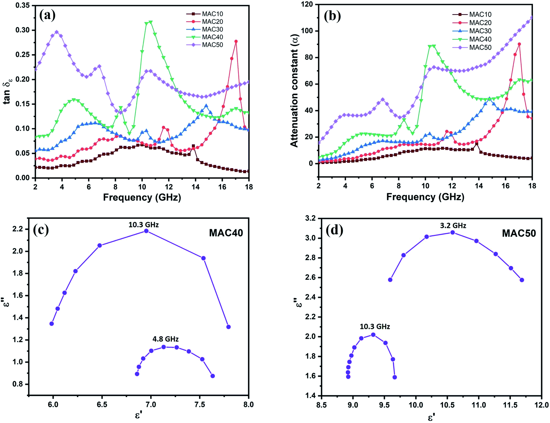 | ||
| Fig. 5 (a) Dielectric loss tangent and (b) attenuation constant (α) of MAC–paraffin wax composites with different filler loadings ranging from 10 wt% to 50 wt%; Cole–Cole plot of (c) MAC40 and (d) MAC50. | ||
Dielectric relaxation plays an important role in the MW absorption performance of an absorber. Based on the Debye dipolar relaxation,14,51 the relationship between ε′ and ε′′ can be written as:
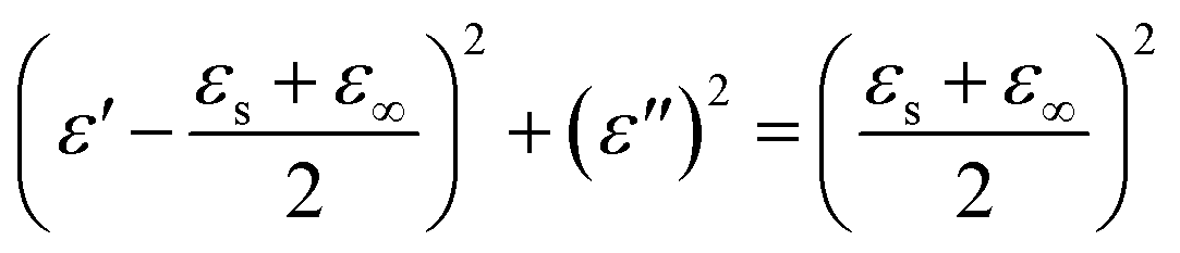 | (5) |
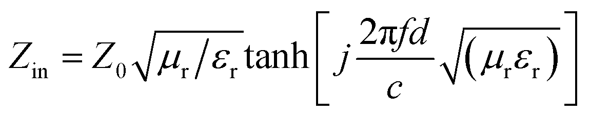
Impedance matching is another important characteristic of an absorber for enhanced MW-absorbing properties. It is represented by the relation Z = |Zin/Z0|, where Z0 denotes the impedance of air.2,23 The closer the value of Z to 1, the greater the amount of microwaves that can enter the absorber and thus reduce the direct reflections of MWs from the surface of an absorber. Fig. S5(a–e)† shows a curve of impedance matching with frequency. The peak values of Z range between 11.43 to 34.63 for MAC10, 7.34 to 11.86 for MAC20, 5.1 to 7.7 for MAC30, 2.68 to 4.52 for MAC40, and 1.36 to 3 for MAC50. It is clear from the Z values that as the filler loading of MAC increases, the absorber exhibits more optimal impedance-matching characteristics.
Fig. 6(a–e) depicts the RL curve for five different loadings of MAC at thicknesses ranging from 2 to 7 mm. At 10 wt% MAC loading (Fig. 6a), the sample did not show any significant RL values, and the low amount of filler loading resulted in low dielectric losses that led to poor MW absorption by MAC10. As the filler loading increased to 20 wt% (MAC20, Fig. 6b), the highest RL value of −31.8 dB at 16.72 GHz (7 mm) was obtained. This enhanced MW-absorbing performance can be attributed to the higher values of α and tanδε along with more optimal impedance matching (Fig. S6†) in the frequency range of 16–17 GHz. Fig. 6c shows the RL curve for MAC30, and due to low attenuation constant values, RL values above −10 dB were only achieved at thicknesses of 6.5 and 7 mm (RLmax = −14.8 GHz, EAB = 1.47 GHz).
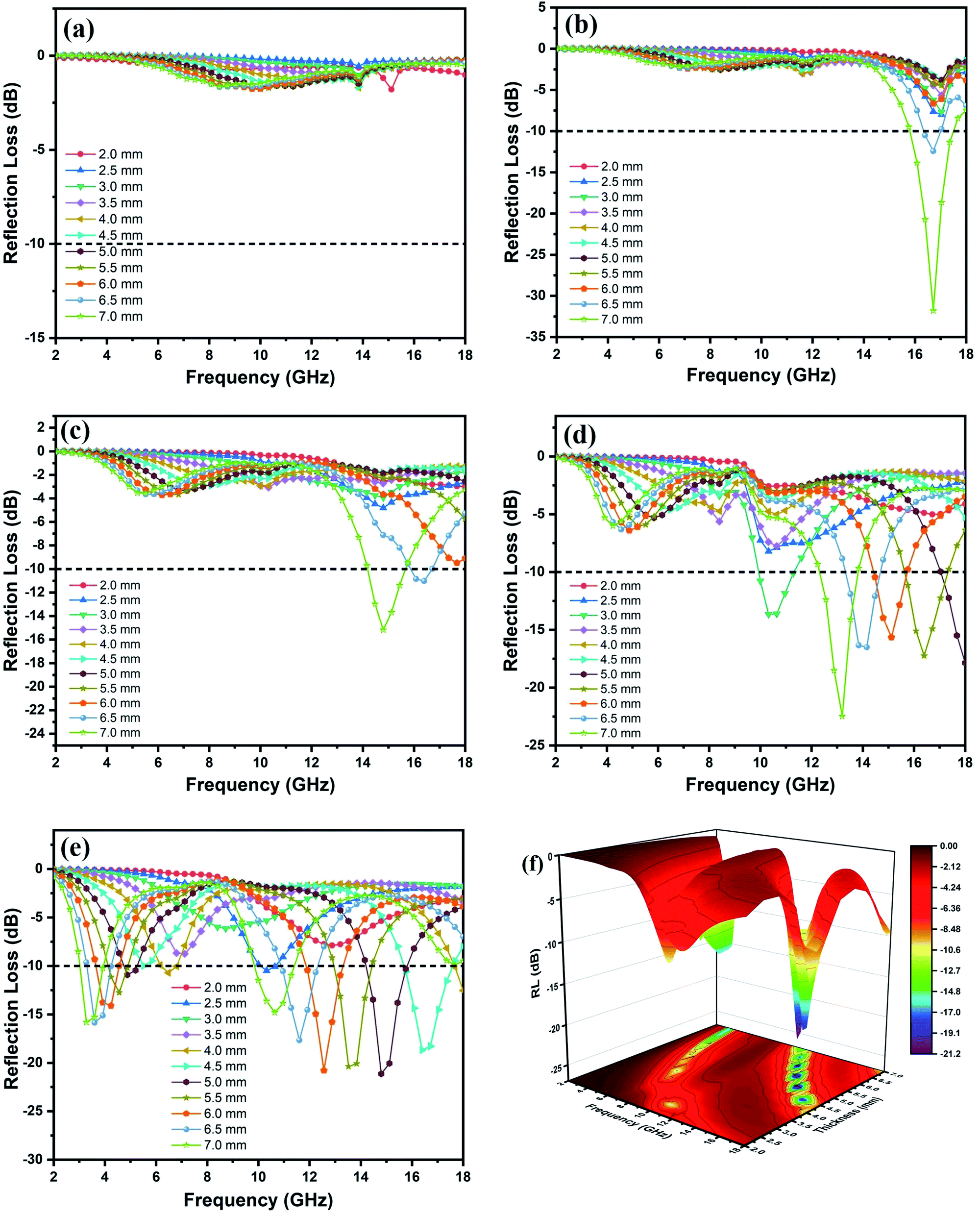 | ||
| Fig. 6 Reflection loss curves of (a) MAC10, (b) MAC20, (c) MAC30 (d) MAC40, (e) MAC50, and (f) 3-D graph of MAC50 at thicknesses ranging from 2 mm to 7 mm. | ||
As the filler loading reached 40 wt% in sample MAC40 (Fig. 6d), the RLmax value of −22.47 dB at 7 mm thickness was achieved, and the RL values below −10 dB for thicknesses of 5–7 mm covered the frequency range from 12.2 to 18 GHz, which included almost the entire Ku band. An EAB of 1.37 GHz at a thickness of only 3 mm was also obtained for the sample. As the filler loading increased from 10 to 40 wt%, one can clearly see an improvement in the RL values in the lower frequency range (4 to 6 GHz), as the RL value reached 5 dB for thicknesses above 5 mm.
Fig. 6e and f show the 2D and 3D RL graph for MAC50, respectively. It clearly depicts the further improvement in the RL values in the frequency range of 3–5.2 GHz, reaching to −15.86 dB for 6.5 mm thickness. Thus, the RL values above −10 dB were achieved in two different frequency bands, i.e., the C and Ku bands, which resulted in dual-band MW absorption characteristics. The RLmax = −21.13 dB was obtained at 14.8 GHz for 5 mm thickness, whereas the maximum EAB of 2.45 GHz was obtained at 7 mm thickness. Therefore, MAC50 contributed the most optimal MW-absorbing performance out of all the samples. The RL <−10 dB covered approximately 10.4 GHz (3–5.2 GHz, 9.8–18 GHz) for various thicknesses.
From Fig. 7a, it is clear that the maximum value of RL gradually shifts towards a lower frequency with the increasing thickness of the absorber. The thickness of an absorber plays an important role in the MW-absorbing performance. This behavior can be explained by the quarter wavelength matching model:26,53
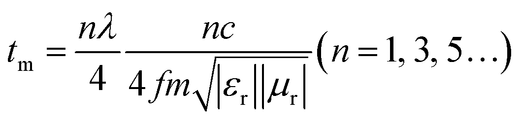 | (6) |
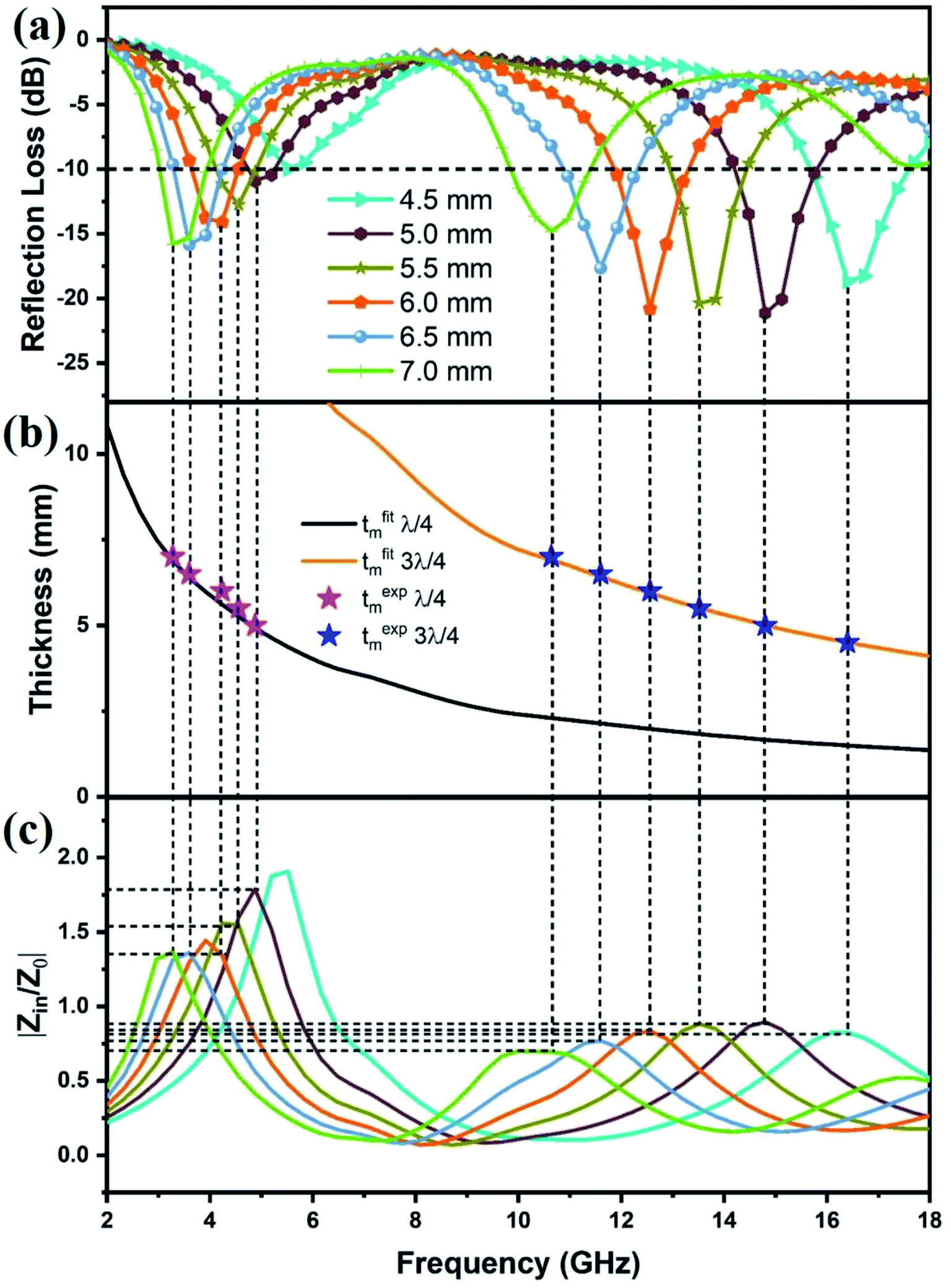 | ||
| Fig. 7 (a) The RL-frequency curves of MAC50 with absorber thickness from 4.5 mm to 7 mm; (b) relationship between tfitm, texpm, and the peak frequency of MAC50 under the nλ/4 model, and (c) the relationship between |Zin/Z0| and frequency for MAC50. | ||
Fig. 7a, c, S7(a, c), and S6† show the relationships between reflection loss and impedance matching for MAC50, MAC40, and MAC20, respectively. It is evident from the graphs that the closer the values of Z to 1, the more optimal the RL values. At 7 mm thickness for MAC20, the value of Z reaches approximately 1, hence, the RL reaches a maximum of −31.8 dB.
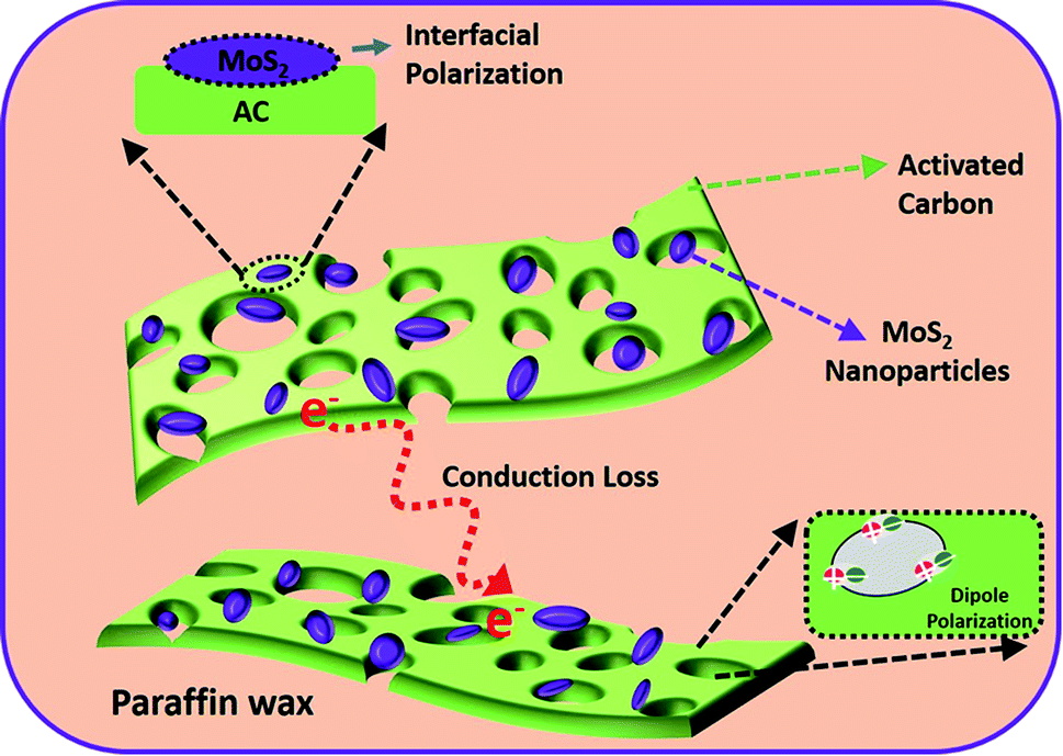
The mechanism for enhanced MW absorption performance in MAC50 can be explained as depicted in Scheme 2. First, the increase in conductivity due to the incorporation of AC resulted in the migration of additional electrons, and those then convert the EM energy by colliding with the lattice,55 leading to high conduction losses.19,23,56 It also improved the impedance matching and reduced the surface reflection of MWs, allowing more MWs to enter the absorber. Second, the combination of AC and MoS2 in the paraffin wax resulted in multiple interfaces, thus increasing the interfacial polarization. Third, the asymmetrical charge distribution due to the pores and defects present in the AC resulted in the formation of dipoles.46 These dipoles under an alternating EM field rotate to align themselves with the EM field and thus convert the EM energy into heat.55 Therefore, it is concluded that MoS2/AC has the potential for MW absorption applications.
 | ||
| Scheme 2 Schematic illustration of the MW absorption mechanism in the MAC–paraffin wax composite. | ||
4. Conclusions
A MoS2/AC composite was successfully synthesized by a hydrothermal method. The incorporation of biomass (mango leaves)-based AC played a key role in improving the MW absorption performance of the MAC composite. The maximum RL value of −31.8 dB was achieved with a filler loading of only 20 wt%. It was also found that a filler loading of 50 wt% MAC in paraffin wax resulted in a unique dual-band absorption property in C and Ku bands. Impressively, an EAB of 10.4 GHz (3–5.2 GHz, 9.8–18 GHz) was achieved at thicknesses ranging from 4.5 mm to 7 mm. The synergistic effects between the MoS2 nanoparticles and AC resulted in high impedance matching, multiple reflections, and improved attenuation constant values, which contributed to the enhancement of the MW absorption properties of MoS2/AC. These results suggest that MoS2/AC is a promising dielectric dual-band MW absorber for practical applications. This study can also be extended to other combinations of biomass-based carbon with MoS2 for designing novel MW absorbers.Conflicts of interest
There are no conflicts to declare.Acknowledgements
Author Praveen Negi is thankful to the Director, National Institute of Technology Kurukshetra for providing Institute fellowship. The authors are also thankful to the Director, DMSRDE, DRDO Kanpur for VNA characterization. Additionally, the authors acknowledge MNIT Jaipur (MRC) for FESEM, HRTEM, and IIT Mandi (AMRC) for XPS characterization.References
- D. Zhang, H. Zhang, J. Cheng, H. Raza, T. Liu, B. Liu, X. Ba, G. Zheng, G. Chen and M. Cao, J. Mater. Chem. C, 2020, 8, 5923–5933 Search PubMed.
- M. Ning, Q. Man, G. Tan, Z. Lei, J. B. Li and R. W. Li, ACS Appl. Mater. Interfaces, 2020, 12, 20785–20796 Search PubMed.
- D. Zhang, J. Chai, J. Cheng, Y. Jia, X. Yang, H. Wang, Z. Zhao, C. Han, G. Shan, W. Zhang, G. Zheng and M. Cao, Appl. Surf. Sci., 2018, 462, 872–882 Search PubMed.
- F. Zhang, W. Zhang, W. Zhu, B. Cheng, H. Qiu and S. Qi, Appl. Surf. Sci., 2019, 463, 182–189 Search PubMed.
- M. Q. Ning, M. M. Lu, J. B. Li, Z. Chen, Y. K. Dou, C. Z. Wang, F. Rehman, M. S. Cao and H. B. Jin, Nanoscale, 2015, 7, 15734–15740 Search PubMed.
- X. Liang, X. Zhang, W. Liu, D. Tang, B. Zhang and G. Ji, J. Mater. Chem. C, 2016, 4, 6816–6821 Search PubMed.
- L. Xing, X. Li, Z. Wu, X. Yu, J. Liu, L. Wang, C. Cai, W. You, G. Chen, J. Ding and R. Che, Chem. Eng. J., 2020, 379, 122241 Search PubMed.
- J. Pan, X. Sun, T. Wang, Z. Zhu, Y. He, W. Xia and J. He, Appl. Surf. Sci., 2018, 457, 271–279 Search PubMed.
- M. Wang, Y. Lin, H. Yang, Y. Qiu and S. Wang, J. Alloys Compd., 2020, 817, 153265 Search PubMed.
- W. Zhang, X. Zhang, Q. Zhu, Y. Zheng, L. F. Liotta and H. Wu, J. Colloid Interface Sci., 2021, 586, 457–468 Search PubMed.
- Y. Sun, W. Zhong, Y. Wang, X. Xu, T. Wang, L. Wu and Y. Du, ACS Appl. Mater. Interfaces, 2017, 9, 34243–34255 Search PubMed.
- L. Lyu, F. Wang, B. Li, X. Zhang, J. Qiao, Y. Yang and J. Liu, J. Colloid Interface Sci., 2021, 586, 613–620 Search PubMed.
- Y. Wang, D. Chen, X. Yin, P. Xu, F. Wu and M. He, ACS Appl. Mater. Interfaces, 2015, 7, 26226–26234 Search PubMed.
- X. Ding, Y. Huang, S. Li, N. Zhang and J. Wang, Composites, Part A, 2016, 90, 424–432 Search PubMed.
- M. Ning, B. Kuang, Z. Hou, L. Wang, J. Li, Y. Zhao and H. Jin, Appl. Surf. Sci., 2019, 470, 899–907 Search PubMed.
- D. Zhang, Y. Jia, J. Cheng, S. Chen, J. Chai, X. Yang, Z. Wu, H. Wang, W. Zhang, Z. Zhao, C. Han, M. Cao and G. P. Zheng, J. Alloys Compd., 2018, 758, 62–71 Search PubMed.
- W. Zhang, X. Zhang, H. Wu, H. Yan and S. Qi, J. Alloys Compd., 2018, 751, 34–42 Search PubMed.
- X. Qiu, L. Wang, H. Zhu, Y. Guan and Q. Zhang, Nanoscale, 2017, 9, 7408–7418 Search PubMed.
- Z. Wu, K. Tian, T. Huang, W. Hu, F. Xie, J. Wang, M. Su and L. Li, ACS Appl. Mater. Interfaces, 2018, 10, 11108–11115 Search PubMed.
- L. Wang, P. Zhou, Y. Guo, J. Zhang, X. Qiu, Y. Guan, M. Yu, H. Zhu and Q. Zhang, RSC Adv., 2019, 9, 9718–9728 Search PubMed.
- H. Zhao, Y. Cheng, H. Lv, G. Ji and Y. Du, Carbon, 2019, 142, 245–253 Search PubMed.
- H. Guan, H. Wang, Y. Zhang, C. Dong, G. Chen, Y. Wang and J. Xie, Appl. Surf. Sci., 2018, 447, 261–268 Search PubMed.
- L. Liu, S. Yang, H. Hu, T. Zhang, Y. Yuan, Y. Li and X. He, ACS Sustainable Chem. Eng., 2019, 7, 1228–1238 Search PubMed.
- P. Negi, A. K. Chhantyal, A. K. Dixit, S. Kumar and A. Kumar, Sustainable Mater. Technol., 2021, 27, e00244 Search PubMed.
- P. Liu, Z. Yao, J. Zhou, Z. Yang and L. B. Kong, J. Mater. Chem. C, 2016, 4, 9738–9749 Search PubMed.
- R. Shu, W. Li, X. Zhou, D. Tian, G. Zhang, Y. Gan, J. Shi and J. He, J. Alloys Compd., 2018, 743, 163–174 Search PubMed.
- W. Gu, J. Sheng, Q. Huang, G. Wang, J. Chen and G. Ji, Nano-Micro Lett., 2021, 13, 102 Search PubMed.
- H. Liu, X. Chen, L. Deng, M. Ding, J. Li and X. He, J. Mater. Chem. A, 2016, 4, 17764–17772 Search PubMed.
- K. S. W. Sing, D. H. Everett, R. A. W. Haul, L. Moscou, R. A. Pierotti, J. Rouquerol and T. Siemieniewska, Pure Appl. Chem., 1985, 57, 603–619 Search PubMed.
- L. Sun, C. Tian, M. Li, X. Meng, L. Wang, R. Wang, J. Yin and H. Fu, J. Mater. Chem. A, 2013, 1, 6462–6470 Search PubMed.
- V. C. Tung, M. J. Allen, Y. Yang and R. B. Kaner, Nat. Nanotechnol., 2009, 4, 25–29 Search PubMed.
- H. Zhou, J. Zhang, I. S. Amiinu, C. Zhang, X. Liu, W. Tu, M. Pan and S. Mu, Phys. Chem. Chem. Phys., 2016, 18, 10392–10399 Search PubMed.
- G. Katumba, B. W. Mwakikunga and T. R. Mothibinyane, Nanoscale Res. Lett., 2008, 3, 421–426 Search PubMed.
- S. Mignuzzi, A. J. Pollard, N. Bonini, B. Brennan, I. S. Gilmore, M. A. Pimenta, D. Richards and D. Roy, Phys. Rev. B, 2015, 91, 195411 Search PubMed.
- G. Mestl, P. Ruiz, B. Delmon and H. Knözinger, J. Phys. Chem., 1994, 98, 11269–11275 Search PubMed.
- B. C. Windom, W. G. Sawyer and D. W. Hahn, Tribol. Lett., 2011, 42, 301–310 Search PubMed.
- C. P. Veeramalai, F. Li, Y. Liu, Z. Xu, T. Guo and T. W. Kim, Appl. Surf. Sci., 2016, 389, 1017–1022 Search PubMed.
- S. V. P. Vattikuti, P. C. Nagajyothi, P. Anil Kumar Reddy, M. Kotesh Kumar, J. Shim and C. Byon, Mater. Res. Lett., 2018, 6, 432–441 Search PubMed.
- H. Liu, H. Hu, J. Wang, P. Niehoff, X. He, E. Paillard, D. Eder, M. Winter and J. Li, ChemElectroChem, 2016, 3, 922–932 Search PubMed.
- Q. Tian, W. Wu, S. Yang, J. Liu, W. Yao, F. Ren and C. Jiang, Nanoscale Res. Lett., 2017, 12, 221 Search PubMed.
- J. Wang, X. Lin, Z. Chu, Z. Huang, T. Guo, L. Yang and S. Li, Nanotechnology, 2020, 31, 135602 Search PubMed.
- L. L. Feng, G. D. Li, Y. Liu, Y. Wu, H. Chen, Y. Wang, Y. C. Zou, D. Wang and X. Zou, ACS Appl. Mater. Interfaces, 2015, 7, 980–988 Search PubMed.
- T. Wu, M. Jing, L. Yang, G. Zou, H. Hou, Y. Zhang, Y. Zhang, X. Cao and X. Ji, Adv. Energy Mater., 2019, 9, 1803478 Search PubMed.
- M. S. Cao, W. L. Song, Z. L. Hou, B. Wen and J. Yuan, Carbon, 2010, 48, 788–796 Search PubMed.
- X. L. Shi, M. S. Cao, J. Yuan, Q. L. Zhao, Y. Q. Kang, X. Y. Fang and Y. J. Chen, Appl. Phys. Lett., 2008, 93, 183118 Search PubMed.
- X. X. Wang, W. Q. Cao, M. S. Cao and J. Yuan, Adv. Mater., 2020, 32, 2002112 Search PubMed.
- L. Yan, J. Liu, S. Zhao, B. Zhang, Z. Gao, H. Ge, Y. Chen, M. Cao and Y. Qin, Nano Res., 2017, 10, 1595–1607 Search PubMed.
- M. Zhang, C. Han, W. Q. Cao, M. S. Cao, H. J. Yang and J. Yuan, Nano-Micro Lett., 2021, 13, 27 Search PubMed.
- Z. Zhang, J. Tan, W. Gu, H. Zhao, J. Zheng, B. Zhang and G. Ji, Chem. Eng. J., 2020, 395, 125190 Search PubMed.
- M. S. Cao, X. X. Wang, M. Zhang, J. C. Shu, W. Q. Cao, H. J. Yang, X. Y. Fang and J. Yuan, Adv. Funct. Mater., 2019, 29, 1807398 Search PubMed.
- W. Gu, X. Cui, J. Zheng, J. Yu, Y. Zhao and G. Ji, J. Mater. Sci. Technol., 2021, 67, 265–272 Search PubMed.
- M. S. Cao, X. X. Wang, M. Zhang, W. Q. Cao, X. Y. Fang and J. Yuan, Adv. Mater., 2020, 32, 1907156 Search PubMed.
- W. Jang, S. Mallesh, S. B. Lee and K. H. Kim, Curr. Appl. Phys., 2020, 20, 525–530 Search PubMed.
- J. Fang, Y. Shang, Z. Chen, W. Wei, Y. Hu, X. Yue and Z. Jiang, J. Mater. Chem. C, 2017, 5, 4695–4705 Search PubMed.
- M. Cao, X. Wang, W. Cao, X. Fang, B. Wen and J. Yuan, Small, 2018, 14, 1800987 Search PubMed.
- B. Quan, W. Gu, J. Sheng, X. Lv, Y. Mao, L. Liu, X. Huang, Z. Tian and G. Ji, Nano Res., 2021, 14, 1495–1501 Search PubMed.
Footnote |
| † Electronic supplementary information (ESI) available: Particle size distribution graph with FESEM images, BET of AC, complex permittivity, Cole–Cole plot, frequency vs. impedance matching curves, RL and thickness graph for MAC20, and combined graph of RL, impedance matching, and thickness for MAC40. See DOI: 10.1039/d1na00292a. |
| This journal is © The Royal Society of Chemistry 2021 |