
 Open Access Article
 This Open Access Article is licensed under a
 Creative Commons Attribution 3.0 Unported Licence
Inverted perovskite solar cells with enhanced lifetime and thermal stability enabled by a metallic tantalum disulfide buffer layer†
Konstantinos
Chatzimanolis
a,
Konstantinos
Rogdakis
 *ab,
Dimitris
Tsikritzis
ab,
Nikolaos
Tzoganakis
a,
Marinos
Tountas
a,
Miron
Krassas
a,
Sebastiano
Bellani
c,
Leyla
Najafi
c,
Beatriz
Martín-García
de,
Reinier
Oropesa-Nuñez
f,
Mirko
Prato
g,
Gabriele
Bianca
dh,
Iva
Plutnarova
i,
Zdeněk
Sofer
i,
Francesco
Bonaccorso
cd and
Emmanuel
Kymakis
*ab
*ab,
Dimitris
Tsikritzis
ab,
Nikolaos
Tzoganakis
a,
Marinos
Tountas
a,
Miron
Krassas
a,
Sebastiano
Bellani
c,
Leyla
Najafi
c,
Beatriz
Martín-García
de,
Reinier
Oropesa-Nuñez
f,
Mirko
Prato
g,
Gabriele
Bianca
dh,
Iva
Plutnarova
i,
Zdeněk
Sofer
i,
Francesco
Bonaccorso
cd and
Emmanuel
Kymakis
*ab
aDepartment of Electrical & Computer Engineering, Hellenic Mediterranean University (HMU), Heraklion 71410, Crete, Greece. E-mail: krogdakis@hmu.gr; kymakis@hmu.gr
bInstitute of Emerging Technologies (i-EMERGE) of HMU Research Center, Heraklion 71410, Crete, Greece
cBeDimensional SpA, Via Lungotorrente Secca 3d, 16163 Genova, Italy
dGraphene Labs, Istituto Italiano di Tecnologia, via Morego 30, Genova, 16163, Italy
eCIC nanoGUNE, Tolosa Hiribidea, 76, 20018 Donostia-San Sebastian, Spain
fDepartment of Materials Science and Engineering, Uppsala University, Box 534, 751 03 Uppsala, Sweden
gMaterials Characterization Facility, Istituto Italiano di Tecnologia, via Morego 30, 16163 Genova, Italy
hDipartimento di Chimica e Chimica Industriale, Università degli Studi di Genova, via Dodecaneso 31, 16146 Genoa, Italy
iDepartment of Inorganic Chemistry, University of Chemistry and Technology Prague, Technická 5, 166 28 Prague 6, Czech Republic
First published on 9th April 2021
Abstract
Perovskite solar cells (PSCs) have proved their potential for delivering high power conversion efficiencies (PCE) alongside low fabrication cost and high versatility. The stability and the PCE of PSCs can readily be improved by implementing engineering approaches that entail the incorporation of two-dimensional (2D) materials across the device's layered configuration. In this work, two-dimensional (2D) 6R-TaS2 flakes were exfoliated and incorporated as a buffer layer in inverted PSCs, enhancing the device's PCE, lifetime and thermal stability. A thin buffer layer of 6R-TaS2 flakes was formed on top of the electron transport layer to facilitate electron extraction, thus improving the overall device performance. The optimized devices reach a PCE of 18.45%, representing a 12% improvement compared to the reference cell. The lifetime stability measurements of the devices under ISOS-L2, ISOS-D1, ISOS-D1I and ISOS-D2I protocols revealed that the TaS2 buffer layer retards the intrinsic, thermally activated degradation processes of the PSCs. Notably, the devices retain more than the 80% of their initial PCE over 330 h under continuous 1 Sun illumination at 65 °C.
Introduction
Organic–inorganic hybrid perovskite solar cells (PSCs) have revealed their potential as excellent solar energy conversion devices, reaching a power conversion efficiency (PCE) of 25.2%.1 The biggest challenge for the further deployment of PSCs is to attain enhanced lifetime stability without reducing device PCE while up-scaling active area and manufacturing processes. Engineering approaches to tackle these issues include the incorporation of two-dimensional (2D) interlayers (e.g., graphene2 and transition metal dichalcogenides (TMDs))3 – a process applicable also in large-area modules4–6 – the optimization of the doping and surface functionalization of 2D interlayers,7 as well the possibility of integrating passivation layers8 such as 2D insulators.9 Therefore, the flexible design of printable PSCs with integrated 2D materials offers many possibilities to discover new properties and functionalities, and constitutes a perfect match for providing power in autonomous Internet of Things (IoT) and wearable systems.10In particular, the engineering of PSC's charge transport layers (CTLs) has a pivotal role in achieving high PCEs and extended device lifetimes.11,12 Thanks to the plethora of their properties, 2D materials are excellent candidates for tuning and/or replacing the hole transport layer (HTL) or electron transport layer (ETL) of PSCs.13–15 For instance, graphene has been extensively used in PSCs as dopant for CTLs for enhancing their carriers' mobility.16–19 Meanwhile, 2D TMDs have been recently incorporated in PSCs due to their unique electrical and optical properties, allowing the energey levels to be aligned across cell's layers.16,20 Among 2D materials, group-VI TMDs (e.g., WSe2, MoS2, MoSe2) and group-XIV metal chalcogenides (e.g., SnS2) have been integrated in PSCs using various approaches. Specifically, 2D MoS2 flakes were used as interlayer over the HTL in inverted21–24 and normal PSCs,7,25 increasing the PCE and the stability, while approaches for HTL replacement were also demonstrated.26 Few-layer flakes of SnS2 were used as ETL material in planar PSC structures, exhibiting PCE values up to 20.1%,27 while WSe2 interlayer over PEDOT:PSS was reported to increase the PCE from 13.8% to 16.2%.28 Finally, inverted PSCs were fabricated through the employment of MoSe2 as HTL29,30 or as buffer layer.31
Differently from the most investigated TMDs, group-V TMDs (e.g., TaS2, NbS2 and VS2) can be found in metal-like phases32,33 such as 2H-, 3R- and 6R polytypes for Nb- or Ta-based TMDs,34,35 and 1T-polytypes for V-based TMDs.36,37 Nevertheless, their unique properties have been rarely used in photovoltaic (PV) systems, and only few studies have recently reported the successful integration of group-V TMDs (mainly TaS2 and NbS2) in PSCs.38,39 These investigations mainly aimed to replace traditional CTLs by bulk or 2D group-V TMDs. For instance, a thin film of metallic TaS2 has been recently used as back contact in Cu2BaSnS4 solar cells as alternative to Mo/MoS2.40 The potential of incorporating 2D TaS2 in PVs was demonstrated by inserting TaS2 nanosheets as HTL (oxidized flakes) or ETL in normal and inverted organic solar cells, respectively, leading to a PCE enhancement – especially for the case of inverted configurations. The PCE improvement was attributed to the favourable energy level alignment between the active layer and the TaS2 CTLs.41 Following a similar approach, TaS2 nanosheets were used to replace SnO2 that served as ETL in normal PSCs, leading to a PCE as high as 15.23%.38
In this study, differently from previous works, we investigated the incorporation of 2D TaS2 flakes in inverted PSCs as efficient buffer layer on top of the ETL, improving both the PCE and the stability of reference devices. More in detail, TaS2 flakes were produced through an up-scalable ultrasonication-assisted liquid-phase exfoliation (LPE) process of the corresponding bulk 6R-TaS2 crystals and then were deposited on the ETL, i.e., PC70BM. The buffer layer formed by TaS2 flakes was optimized by varying the number of consequent spin coatings (SCs). The PSCs incorporating the TaS2 buffer layer demonstrated a PCE value of 18.45%, corresponding to a 12% improvement compared to the reference device (PCE = 17.66%). The enhanced performance is attributed to the excellent charge transport properties and suitable work function (WF) of TaS2 flakes, matching the energy level of the in-contact materials. More importantly, the TaS2-enabled devices exhibited an improved lifetime and thermal stability when tested under ISOS-L2, ISOS-D1I and ISOS-D2I protocols. The optimized devices showed a degradation rate of 0.061% PCE per h and retained more than the 80% of their initial PCE for 330 h under continuous 1 Sun AM1.5G illumination.
Experimental
Synthesis and exfoliation of 6R-TaS2 crystals
6R-TaS2 crystals were prepared through direct synthesis from elements, i.e., Ta and S, following protocols previously reported in literature.42 Experimentally, amounts of Ta (99.999%, <6 μm) and S (99.9%, <100 μm) powders (Strem Chemicals, Inc.), with a S![[thin space (1/6-em)]](https://www.rsc.org/images/entities/char_2009.gif) :Ta stoichiometry of 2:1, were placed in a quartz glass ampoule (20 mm × 120 mm). Once evacuated until a pressure of 1 × 10⁻³ Pa, the ampoule was sealed using an oxygen–hydrogen welding torch. The ampoule was heated to 450 °C for 12 h, and subsequently heated to 600 °C for 48 h, and up to 900 °C for 48 h. Afterwards, the ampoule was cooled down to room temperature over 24 h. The heating rate was +5 °C min−1 for all the heating steps. The TaS2 flakes were produced by ultrasonication-assisted LPE of fragments of 6R-TaS2 crystals,42–44 followed by sedimentation-based separation (SBS),45 in anhydrous isopropanol (IPA). Briefly, 50 mg of crystal fragments were inserted in 50 mL of anhydrous IPA. The resulting mixture was ultrasonicated in a sonicator (Branson® 5800 cleaner, Branson Ultrasonics) for 6 h. Then, the dispersion was ultracentrifuged using a Beckman Coulter centrifuge (Optima™ XE-90 with a SW32Ti rotor) at 2700g for 20 min at 15 °C to separate the exfoliated materials (as supernatant) from the unexfoliated bulk crystals (sediment). Lastly, the TaS2 flakes were collected by pipetting 80% of the supernatant. The concentration of the so-produced TaS2 nanoflakes dispersion was fixed to 1 mg mL−1 by adjusting the amount of IPA.
:Ta stoichiometry of 2:1, were placed in a quartz glass ampoule (20 mm × 120 mm). Once evacuated until a pressure of 1 × 10⁻³ Pa, the ampoule was sealed using an oxygen–hydrogen welding torch. The ampoule was heated to 450 °C for 12 h, and subsequently heated to 600 °C for 48 h, and up to 900 °C for 48 h. Afterwards, the ampoule was cooled down to room temperature over 24 h. The heating rate was +5 °C min−1 for all the heating steps. The TaS2 flakes were produced by ultrasonication-assisted LPE of fragments of 6R-TaS2 crystals,42–44 followed by sedimentation-based separation (SBS),45 in anhydrous isopropanol (IPA). Briefly, 50 mg of crystal fragments were inserted in 50 mL of anhydrous IPA. The resulting mixture was ultrasonicated in a sonicator (Branson® 5800 cleaner, Branson Ultrasonics) for 6 h. Then, the dispersion was ultracentrifuged using a Beckman Coulter centrifuge (Optima™ XE-90 with a SW32Ti rotor) at 2700g for 20 min at 15 °C to separate the exfoliated materials (as supernatant) from the unexfoliated bulk crystals (sediment). Lastly, the TaS2 flakes were collected by pipetting 80% of the supernatant. The concentration of the so-produced TaS2 nanoflakes dispersion was fixed to 1 mg mL−1 by adjusting the amount of IPA.
Materials characterization
Scanning electron microscopy (SEM) measurements of the as-synthetized 6R-TaS2 crystals were acquired using JEOL® JSM-6490LA SEM equipped with an energy-dispersive X-ray spectroscopy (EDS) detector, operating at 20 kV. The samples were imaged without any metal coating or pre-treatment.Bright-filed transmission electron microscopy (BF-TEM) measurements of the TaS2 flakes were performed with a JEM 1011 (JEOL) TEM (thermionic W filament), operating at 100 kV. ImageJ software (NIH) and OriginPro 9.1 software (OriginLab) were used to analyse the images and to perform the statistical analysis of the flakes' lateral dimension data, respectively. The samples were fabricated by depositing the LPE-produced TaS2 flake dispersions onto ultrathin C-on-holey C-coated Cu grids. The samples were rinsed with deionized water and subsequently dried overnight under vacuum before to their imaging.
Atomic force microscopy (AFM) measurements were performed using a Nanowizard III (JPK Instruments, Germany), mounted on an Axio Observer D1 (Carl Zeiss, Germany) inverted optical microscope. The images were acquired using a PPP-NCHR cantilevers (Nanosensors, USA), which have a tip with a nominal diameter of 10 nm. The image acquisition was performed using a drive frequency of ∼295 kHz. Intermittent contact mode was used to record the image over an area of 2.5 × 2.5 μm2 (512 × 512 data points), using a scan rate of 0.7 Hz. The working set point was set above 70% of the free oscillation amplitude. JPK Data Processing software (JPK Instruments, Germany) and OriginPro 9.1 software were used to elaborate the height profiles and to perform the statistical analysis of the flakes' thickness data. The samples were produced by depositing the LPE-produced TaS2 flake dispersions on substrates of mica (G250-1, Agar Scientific Ltd.). Before the measurements, the samples were dried under vacuum overnight.
X-ray diffraction (XRD) characterization was carried out using a PANalytical Empyrean with Cu Kα radiation. The samples were produced by depositing powder of 6R-TaS2 crystals or LPE-produced TaS2 flake dispersions onto Si/SiO2 substrates. Before the measurements, the samples were dried under vacuum overnight to remove moisture or solvent residuals.
Raman spectroscopy measurements were carried out using a Renishaw microRaman Invia 1000 mounting a 50× objective. The excitation wavelength the incident power on the samples were 532 nm and 1 mW, respectively. The samples were prepared following the procedure described for the XRD characterization.
Kelvin probe force microscopy (KPFM) images were acquired in air with a XE7 AFM (Park System, Korea) and low-noise lock-in amplifier SR830 DSP (Stanford research systems, USA) operating in AM mode equipped with Au-coated PPP-NCSTAu cantilevers (Nanosensors, Switzerland) having a tip diameter less than 50 nm. The topography images were collected in non-contact mode using the resonant oscillation of the cantilever (160 kHz) and the potential images were collected using an AC modulation voltage of 0.5 V at 17 kHz applied to the tip. The scan rate for the acquisition of the images was 0.1–0.2 Hz. The samples were prepared by spin-coating a droplet of the TaS2 flakes dispersion onto ITO.
Ultraviolet photoelectron spectroscopy (UPS) with He I (hν = 21.2 eV) radiation was performed using a Kratos Axis UltraDLD spectrometer, operating at <10−8 mbar. A −9.0 V bias was applied to the sample to precisely determine the low kinetic energy cut-off.
Device fabrication
Pre-patterned ITO/glass substrates were cleaned in ultrasonic bath using deionised water, acetone, and IPA. Then, the samples were transferred in N2 glovebox, where they underwent a UV–ozone treatment for 15 min. Thin (∼10 nm) films of poly[bis(4-phenyl)(2,4,6-trimethylphenyl)amine] (PTAA) (Solaris Mw = 20–70 kDa) were prepared by spin coating a 2 mg mL−1 PTAA solution in toluene at an angular speed of 6000 rpm. The PTAA films were annealed at 110 °C for 10 min. The perovskite solution was prepared by mixing 0.2 M methylammonium bromide (MABr) (GreatCell Solar), 1.14 M formamidinium iodide (FAI) (GreatCell Solar), 0.2 M PbBr2 (TCI America) and 1.24 M PbI2 (TCI America) in 4:1 v/v anhydrous dimethylformamide (DMF) (99.8%, Sigma Aldrich):dimethyl sulfoxide (DMSO) (99.9%, Sigma Aldrich) and then adding 5 vol% from a 1.5 M CsI stock solution and 4 vol% from 1.5 M RbI stock solution. The perovskite layers were spin coated on the PTAA film at 6000 rpm for 45 s. 10 s prior to the end of the spinning process, 200 mL of anhydrous chlorobenzene (CB) (99.8%, Sigma Aldrich) was dropped onto the spinning perovskite film. Subsequently, the samples were immediately annealed for 45 min on a hotplate preheated at 100 °C. Next, thin-layers of PC70BM (99%, Solenne) were deposited by spin coating a 20 mg mL−1 PC70BM solution in anhydrous CB onto the perovskite at 1000 rpm. The PSCs were then completed following a procedure described in ref. 8. Briefly, the TaS2 flakes were deposited from their dispersions onto PC70BM through consecutive SCs (up to five). Afterwards, 45 mL of 0.5 mg mL−1 bathocuproine (BCP) (96%, Sigma Aldrich) prepared in IPA (99.5% extra dry, ACROS Organics) was spin coated onto the TaS2 buffer layers. Finally, a 100 nm-thick Ag top electrode was deposited by vacuum thermal evaporation.
Device characterization
The PSCs were evaluated under an inert atmosphere using an ABB solar simulator (Sol1A, Oriel) equipped with a 450 W Xe lamp and an AM1.5G filter. The intensity was calibrated at 100 mW cm−2 using a KG3-window Si reference cell. The J–V curves were recorded at a constant scan rate of 20 mV s−1 using a multiplexor test board system (Ossila), and no device preconditioning was applied before the measurements. A black metallic aperture mask was used during each measurement to set the active area of the fabricated devices at 0.04 cm2 and to reduce the influence of the scattered light. The external quantum efficiency (EQE) spectra were recorded using a QE-T system from Enlitech. A chopping frequency of 60 Hz was used. The calibration of the light intensity was performed using a quartz-window Si solar cell. The integrated current density was calculated by integrating the product between the spectral response of the test cell and the reference AM1.5G solar spectrum. Optoelectrical characterization was performed with a transient module of ARKEO measurement platform (Cicci Research s.r.l.). Transient photovoltage (TPV) experiments were performed in small perturbation mode by confining the intensity of the light pulse to less than 10% of the background voltage, unaltering the equilibrium of the field induced by the background bias. The voltage decay of the measured devices was fitted by an exponential decay with a time constant that directly reflects the lifetime of the charge carriers. Transient photocurrent (TPC) experiments were performed in both large and small perturbation regimes. Large perturbations were induced over 200 ms under a 0.8 duty cycle, while small perturbations were loaded with a 0.001 cycle and passed through an external circuit of 50 ohm resistance. Both the signals of open circuit voltage, Voc, (for TPV) and short circuit current, Jsc, (for TPC) were monitored after passing them through voltage and impedance amplifiers. To observe the photoinduced charge extraction through linearly increasing voltage (photo-CELIV) measurements, a 470 nm fast LED source driven by a 100 mA current and exhibiting a Lambertian radiation pattern was used. The relaxation pulse width was set to 20 ms, charged by a 50000 V s−1 ramp, following a 13 ms delay after the injection pulse. The collected signals were processed through a transimpedance amplifier and passed through a 100 MHz bandwidth digitizer running in single-shot mode. The lifetime behaviour of the PSCs was monitored using an ISOS testing laboratory from InfinityPV in ISOS-L2 operation mode. The devices were first encapsulated with a piece of glass and a UV-curable epoxy as an adhesive (Ossila E132). Then, the devices were placed inside the test chamber and exposed to continuous illumination. The apparatus was equipped with a solar simulator using a metal halide light source simulating the AM1.5 G spectrum in the range of 300–900 nm. The light intensity was calibrated at 100 mW cm−2 using a Si reference cell. The humidity in the test chamber was below 15%, while the temperature was over 65 °C. Between the J–V measurements, the devices were left in open circuit condition. The shelf lifetime measurement of the unencapsulated devices was performed in the glove box either at room temperature (ISOS D1I) or at 65 °C (ISOS D2I).
Results and discussion
The as-synthesized 6R-TaS2 crystal was characterized by SEM-EDS measurements (see ESI, Fig. S1a–c†), showing crystal fragment with nearly straight borders and a S:Ta atomic ratio of 1.9 ± 0.2, which is similar to the values previously measured for TaS2 produced with similar protocols.42,44,46,47 Fig. S1d† shows a SEM image zooming a crystal edge, evidencing the layered structure the 6R-TaS2 crystals. Transmission electron microscopy and AFM measurements were performed to evaluate the lateral size and thickness of the TaS2 flakes produced through LPE of fragments of 6R-TaS2 crystals in anhydrous IPA. Fig. S2a† shows a BF-TEM image of representative TaS2 flakes, exhibiting irregular shapes with flat surfaces and nearly straight edges. The data of the lateral size of the flakes follow a log-normal distribution peaked at ∼25 nm, with an average value of 87.6 nm (Fig. S2b†). Fig. S2c† reports an AFM image of representative TaS2 flakes. The statistical analysis of the thickness data indicate that they follow a log-normal distribution peaked at ∼1.7 nm (Fig. S2d†). Since the AFM thickness of TaS2 monolayer typically lies between 0.4 and 0.9 nm (depending on the TaS2/substrate interaction and AFM instrumentation),48,49 these results indicate that the exfoliated TaS2 sample mainly consists of single-/few-layer flakes. The structural properties of the TaS2 flakes were evaluated through XRD and Raman spectroscopy measurements. Fig. S3a† reports the XRD pattern of the TaS2 flakes in comparison to the one recorded for the native bulk crystal. Both the XRD patterns shows reflections which match those of the 6R phase ((ICSD-52117), although a secondary 2H phase (ICSD-68488) coexists with a marginal contribution, as observed by previous studies on 6R-TaS2 polytypes.42 Fig. S3b† shows the Raman spectra of both bulk and exfoliated TaS2 samples, further confirming their crystal structure. Noteworthy, 6R-TaS2 polytype exhibits Raman modes similar to those of 2H polytype, namely the out-of-plane vibration A1g mode at ∼380 cm−1, the in-plane vibrational E12g mode at ∼280 cm−1 and the broad second-order peak attributed to two-phonon process at ∼180 cm−1.50,51 The TaS2 flakes retain the position of the A1g mode of the bulk crystals. Differently, E12g is blue-shifted by ∼17 cm−1, because of the decrease of long-range Coulomb interlayer interactions with decreasing the number of layers.52 Moreover, the two-phonon peak is red-shifted by 22 cm−1, which may be consequence of the emergence of the E1g mode.53 The latter can be activated by the symmetry breaking caused by interaction of single/few layer nanoflakes with SiO2/Si substrate.54 The layers with octahedral Ta coordination may also contribute with Raman mode resembling those exhibited by 1T-TaS2 polytypes, which typically shows peaks at ∼250, ∼310 and ∼380 cm−1.55–58
To investigate the energetics of the TaS2 flakes, the latter were deposited on ITO and characterized by KPFM. Fig. S4† displays a 3D representation of surface topography including an overlayer of the Contact Potential Difference (CPD). Interestingly, at the places where TaS2 flakes were deposited, the CPD increase by 15 mV compared to the substrate values. These data indicate that the WF of the TaS2 flakes is lower than the one of the ITO.59 Lastly, UPS measurements were performed to quantitatively estimate the WF of a film of TaS2 flakes. Fig. S5a† shows the secondary electron cut-off region of the spectrum indicating a cut-off energy of ∼17.1 eV, corresponding to a WF of 4.1 eV. Noteworthy, the LPE process is effective to reduce the WF of the 6R-TaS2 bulk crystal, which is 3.9 eV (Fig. S5b†). This means that the exfoliation of the material can tune the energy barrier between the PC70BM LUMO (4.0 eV) to improve the electron extraction process from PC70BM to 6R-TaS2 (see the details on the PSC structure in the next section). Although the LPE process duration may further improve the electron extracting properties of the 6R-TaS2 flakes, the concomitant reduction of the lateral dimension of the flakes may negatively affect the protective properties of the 6R-TaS2 flakes against volatile species and ion migration, as demonstrated later in the text. Therefore, we limited the exfoliation of the flakes without prolonging further the LPE process. Fig. S5c and d,† show the regions near the Fermi energy level of the UPS spectra for both bulk and exfoliated 6R-TaS2 crystals. The presence of an “edge” centred at the zero of the binding energy scale confirms the metallic character of the 6R phase of TaS2, in agreement with previous literature.42
Structural and morphological characterization of PSCs
Fig. 1 shows a schematic illustration of an inverted PSC, which consists of a glass/ITO/PTAA/perovskite/PC70BM/TaS2/BCP/Ag material stack. Based on the characterization of the TaS2 flakes (Fig. S1–S5†), the WF of 4.1 eV and the metallic character of the material indicate that TaS2 buffer layers over the PC70BM can effectively passivate interfacial defects and pin-holes,60–62 while improving the energy level alignment at the interface between the ETL and Ag electrode63 that has a WF of ∼4.3 eV.64 Hereafter, PSC-1, -2, -3 and -5 refers to a device incorporating TaS2 buffer layers obtained through 1, 2, 3 and 5 SCs, respectively.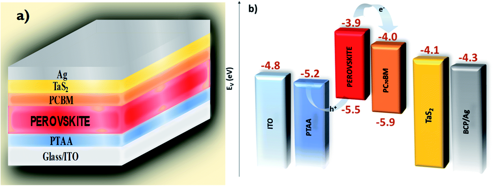 | ||
| Fig. 1 (a) Schematic illustration of an inverted PSC incorporating 6R-TaS2 flakes, with the following layered stack: Glass/ITO/PTAA/Perovskite/PC70BM/TaS2/Ag. (b) Energy level diagram of the material stack in the PSC. | ||
Scanning electron measurements (FEI Helios Nanolab 450S microscope −5 kV and 0.2 nA imaging conditions) were performed to elucidate the layered structures of both reference PSC without TaS2 buffer layer (PSC-Ref) and PSC-2 (Fig. 2a, c and b, d, respectively). Fig. 2a shows the surface of the perovskite layered in PSC-Ref, revealing crystal grain sizes of ca. 250 nm. Fig. 2b shows the top-view of the TaS2 buffer layer deposited over PC70BM layer. Since most of the flakes have nanometric thicknesses (see Fig. S2c and d†), only occasional thick TaS2 flakes are clearly distinguished by SEM imaging. Nevertheless, SEM-EDS analysis (FEI Quanta 250 FEG microscope, acquiring at 30 kV) (Fig. S6b and c†) confirmed the homogeneous presence of TaS2 flakes on the PC70BM surface. Fig. 2c depicts a cross-section of the layered structure (made by focused ion beam, dual-beam FEI Helios Nanolab 450S microscope) of the complete reference device, showing a perovskite layer with a thickness of about 350–400 nm. As shown in the cross-sectional SEM image of PSC-2 (Fig. 2d), the device structure is not significantly affected by the incorporation of the few-nm thick TaS2 buffer layer.
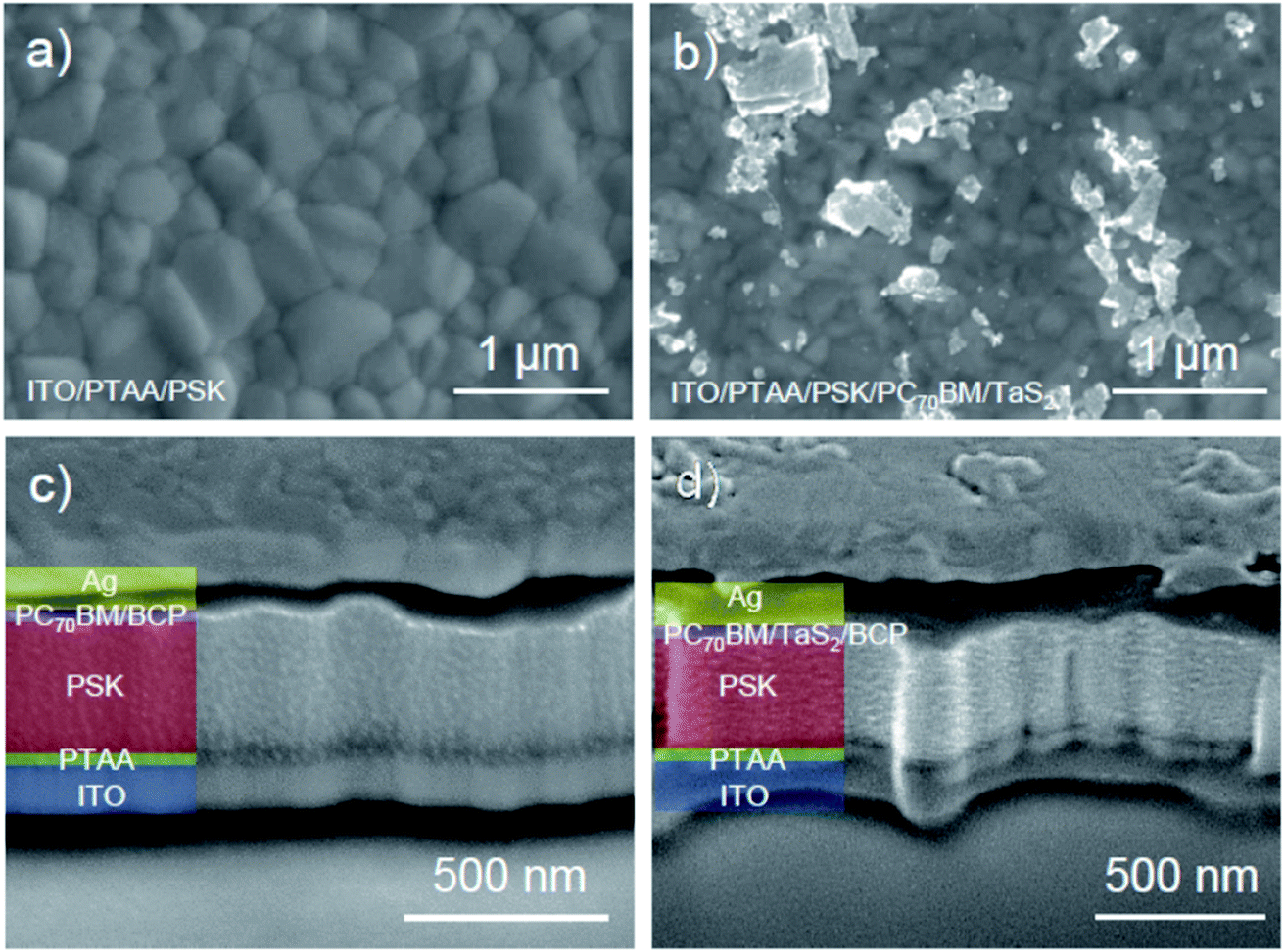 | ||
| Fig. 2 Representative top-view and cross-sectional SEM images of PSC-Ref (panels a, c) and PSC-2 (panels b, d). (a) Top-view of perovskite surface prior to PCBM deposition in PSC-Ref. (b) Top-view of the 6R-TaS2 buffer layer on top of the PC70BM layer. (c) Cross-sectional SEM image of PSC-Ref. (d) Cross-section SEM image of PSC-2 incorporating the TaS2 buffer layer. False colouring was used for the different layers of the structure: ITO/PTAA/perovskite (PSK)/PC70BM/Ag. | ||
Steady state photovoltaic characterization of PSC devices
The PV performance of the investigated PSCs was evaluated as a function of the number of consecutive SCs of the TaS2 flakes dispersion on top of the PC70BM. As shown in Fig. 3a, the PV performance of the devices is improved upon TaS2 flakes deposition, except when the total number of SCs is more than three. The maximum PCE performance was recorded for PSC-1 and PSC-2 devices (average PCE of 17.5% and 17.4%, respectively), while the average PCE of PSC-3 (17.3%) also remained higher than the one recorded for PSC-Ref (∼16.6%). By increasing the number of the SCs to more than 3, the average PCE decreases to 15.74% because of the enhanced electron scattering rate as the thickness of the TaS2 buffer layer increases. Moreover, the excessive IPA exposure of the device for 5 SCs is detrimental for the device performance.31Fig. 3b shows the J–V curves of the champion PSC-1, PSC-2, PSC-3, PSC-5 and PSC-Ref, while Table 1 summarizes the main device PV parameters extracted from the J–V curves analysis, i.e.: average and maximum values of PCE, open circuit voltage (Voc), short circuit current density (Jsc) and fill factor (FF). The average PCE improves from 16.57% in PSC-Ref to 17.53%, 17.36% and 17.30% for the PSC-1, PSC-2 and PSC-3, respectively and drops to 15.74% in PSC-5. The champion device (PSC-3) achieved a PCE up to 18.45%, representing a +12% PCE improvement compared to the best PSC-Ref (PCE = 17.66%). All devices exhibited negligible hysteresis, as revealed by their reverse J–V scan analysis shown in Fig. S7 and Table S1.† Moreover, the steady-state PCE of the devices was quite stable, as shown in Fig. S7b,† where the Jsc stabilized after 120 s after a slight initial increase. Fig. S7c† shows the EQE spectrum of the most performant device together with the calculated current density, which matches the Jsc. Fig. S8† shows the photoluminescence (PL) measurements of samples fabricated up to perovskite layer, as well as samples containing also PC70BM and TaS2 layers. The addition of PC70BM ETL on top of the perovskite causes PL quenching because of a more efficient electron extraction by the PC70BM. Meanwhile, the PL peak is red-shifted from 790 nm in the ETL-free sample to 793 nm. The red-shift can be attributed to an enhanced photon recycling due to the metallic 2D-flakes.65,66 The incorporation of the TaS2 buffer layer does not increase further the PL quenching. | ||
| Fig. 3 Photovoltaic performance of the reference PSC (PSC-Ref) and the PSCs incorporating TaS2 flakes as a buffer layer (PSC-X). (a) Box chart of PCE performance for PSC-Ref, PSC-1, PSC-2 PSC-3 and PSC-5, and (b) the J–V curves measured for the champion devices for each PSC configuration. | ||
| PCE (%) | V oc (V) | J sc (mA cm−1) | FF (%) | |
|---|---|---|---|---|
| PSC-Ref | 16.57 ± 0.43 (17.66) | 1.067 ± 0.022 (1.081) | 20.71 ± 0.58 (20.84) | 74.16 ± 1.66 (78.37) |
| PSC-1 | 17.53 ± 0.50 (18.28) | 1.077 ± 0.021 (1.070) | 21.25 ± 0.43 (21.56) | 75.48 ± 2.45 (79.22) |
| PSC-2 | 17.36 ± 0.12 (18.10) | 1.088 ± 0.020 (1.096) | 21.41 ± 0.52 (21.98) | 73.87 ± 1.87 (75.09) |
| PSC-3 | 17.30 ± 0.60 (18.45) | 1.068 ± 0.020 (1.080) | 21.29 ± 0.45 (21.45) | 75.07 ± 2.20 (79.65) |
| PSC-5 | 15.74 ± 0.50 (16.06) | 1.048 ± 0.018 (1.036) | 20.01 ± 0.42 (20.15) | 74.29 ± 1.58 (76.86) |
Transient photovoltage characterization of PSC devices
Transient photovoltage and TPC measurements were performed to explain the physical mechanism behind the performance enhancement reported when the TaS2 flakes are incorporated into the PSCs as a buffer layer. Fig. 4a shows the comparison between the lifetime decay of PSC-1, PSC-3, and PSC-Ref. The carrier lifetimes were extracted from corresponding transient tail of TPV decay curves (Fig. S9†) that follow a single exponential trend.27 In particular, TPV results show that the TaS2 buffer layer reduces the charge recombination rate and increases the charge carrier lifetime (Fig. 4a), which is consistent with the highest Voc measured for TaS2-based devices (see Fig. 3a and Table 1). Furthermore, the addition of the TaS2 buffer layer does not significantly affect the distribution of shallow defect states (see inset panels in Fig. S9†). Transient photocurrent experiments in charge extraction mode demonstrated that the TaS2 buffer layer increases the overall extracted charge density, especially in the PSC-1 device (Fig. 4b). These data suggest that the metallic character of the TaS2 flakes (see Fig. S5b†) play a beneficial role in the charge extraction process. The measurements performed in the high perturbation regime (0.8 duty cycle) show the absence of deep trap states in all the tested samples (Fig. S10†). | ||
| Fig. 4 Estimation of the carrier's lifetime, the extracted charge density, as well as the effective carrier mobility, based on transient measurements. (a) Extracted carrier's lifetime from TPV decay measurements at different bias conditions. (b) Charge density extracted from TPC measurements. The lines in panels (a, b) represent linear fittings. (c) Drift mobility estimation from the photo-CELIV technique. | ||
The drift mobility of electrons/holes was probed using charge extraction by linearly increasing voltage (photo-CELIV) under various light pulse delay points. More in detail, the drift mobility was derived from the extracted charge represented by the part of the transient superimposed over the displacement current level (Fig. S11†). The mobility (μ) can be derived according to the equation:27

Lifetime and thermal stability measurements of perovskite devices
Various approaches have been proposed to enhance the stability of PSCs and related modules, which still suffer of significant degradation over timescale required for commercial applications.67–69 Here, the lifetime and shelf stability of the devices incorporating the TaS2 buffer layer were probed either under inert or ambient atmosphere in accordance with the updated ISOS protocols (ISOS-L2, D1I, -D2I, -D1).70 The updated ISOS protocols were designed to cover emerging PV technologies with distinctive characteristics (e.g., light soaking effect and volatile nature of organic species) compared to commercially available solar cells. These technologies include the PSCs, which require specific treatment. Apart from measurements under continuous illumination at elevated temperature (ISOS-L2), measurements under N2 atmosphere were also implemented by investigating the shelf life of the devices and the thermal stability at 65 °C though ISOS-D1I and ISOS-D2l protocols, respectively. Finally, we evaluated the shelf life of our devices (unencapsulated) in ambient conditions (ISOS-D1).Under continuous illumination at elevated temperature, the PSC-Ref exhibited a drop of its initial PCE by 50% after 35 h (T50) and lost more than the 70% of its initial PCE after 100 h (Fig. 5). The incorporation of TaS2 buffer layer significantly improved the device stability. In particular, the PSC-1 reported an excellent stability performance, showing a T50 of over 300 h, while its PCE did not drop below 40% even after 600 h. Notably, the best performing device PSC-2 displayed a T50 of more than 600 h. The best stability of PSC-2 can be associated to the optimal surface coverage of the TaS2 buffer layer obtained through two SCs. By further increasing the number of SCs, the stability of the device decreases probably because of excessive exposure of the perovskite to IPA.27 Nevertheless, PSC-3 and PSC-5 are still outperforming the PSC-Ref in terms of lifetime stability. These results indicate that the TaS2 buffer layer between the PC70BM and the Ag metal can serve as a protective layer, retarding device degradation under continuous illumination and thermal stresses.
 | ||
| Fig. 5 Lifetime measurements of encapsulated perovskite devices under continuous 1 sun illumination, 65 °C and 10–15% RH. (a) Long term ISOS-L2 lifetime measurements of PSC-Ref (black), PSC-1 (red), PSC-2 (magenta), PSC-3 (green) and PSC-5 (blue). (b) Normalized PCE over time for PSC-2. The degradation rate is calculated from a linear fit of the experimental data in the stabilized region. Tburn-in marks the end of the burn-in phase and Ts80 denotes the time at which the PCE drops to 80% of the initial PCE at Tburn-in in the stabilized region. | ||
As shown in Fig. 5b, the lifetime stability measurement of the most stable PSC-2 reveals a burn-in phase lasting for about 80 h. During this phase, the initial PCE drops rapidly by about 20%, and afterwards stabilizes with a slow linear decline. The burn-in behaviour is common in organic PVs71,72 and is even often observed in PSCs.73–75 However, in the latter case, the initial losses are often recovered when devices are left to rest under dark conditions.76 Therefore, the linear decay regime of the device was used to estimate the device lifetime. By considering the time at the end of the burn-in phase (Tburn-in), the time at which the PCE drops by 20% compared to Tburn-in, Ts80 represents a usual metric for the PSC stability. The linear fit of the experimental data in the linear regime enables the degradation rate to be estimated. In particular, the estimated degradation slope of PSC-2 was 0.061% h−1. Hence, the device incorporating the TaS2 buffer layer are expected to retain 80% of their initial PCE for 330 h under continuous 1 Sun illumination.
Apart from ISOS-L2 protocols, the device stability was also evaluated by stressing the devices in inert atmosphere under ISOS-D1I and ISOS-D2l protocols. Fig. 6a shows the shelf lifetime of the PSC-Ref and PSC-2 stored in N2 atmosphere with 0% relative humidity (RH) at room temperature and at elevated temperature of 65 °C (Fig. 6b). Importantly, the PSC-2 showed a better stability compared to PSC-Ref (under ISOS-D1I), retaining more than 85% of initial PCE after 50 days of storage (PSC-Ref retained more than 85% of the initial PCE for only 20 days of storage) (Fig. 6a). The beneficial role of TaS2 protective buffer layer appeared also during ISOS-D2l stability tests (Fig. 6b), in which PSC-2 exhibited a superior thermal stability compared to PSC-Ref, retaining more than 60% of the initial PCE after 120 h (PSC-Ref retained only 43% of the initial PCE over the same time interval). The diffusion of the metal and of volatile species through the device and their reactivity to form metal halides have been recognized as the main intrinsic degradation pathway, which can be accelerated through heating.77–80 Thus, the improved thermal stability of the devices with TaS2 flakes can be directly correlated to a reduced diffusion rate of the volatile organic species, and a limited metal diffusion, both enabled by the TaS2 buffer layer.
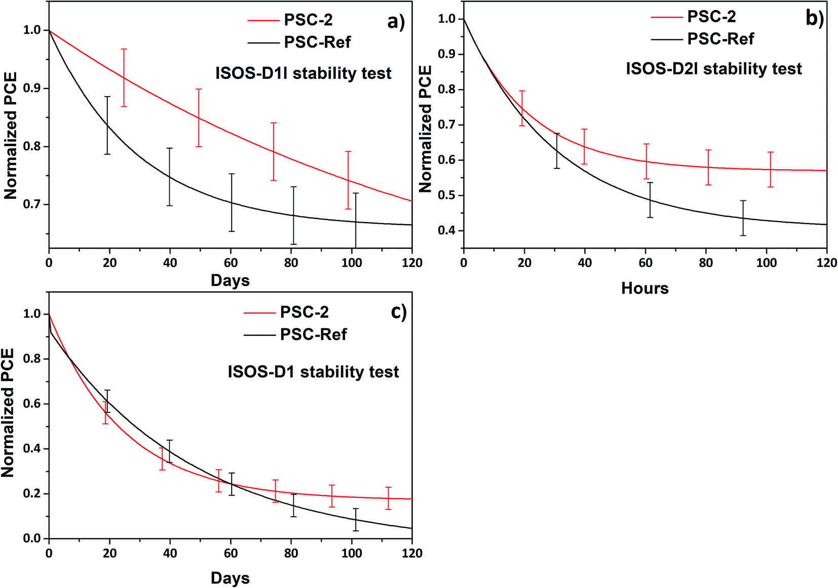 | ||
| Fig. 6 Lifetime measurements for PSC-2 (red), compared to those of PSC-Ref (black) using the following stress factors: (a) under inert atmosphere and 0% RH in the dark, (b) thermal stress at 65 °C under inert conditions and 0% RH and (c) under ambient conditions in the dark of unencapsulated cells. | ||
To better understand the protection role of TaS2 layer, ISOS-D1 measurements were carry out by storing unencapsulated cells at ambient conditions at room temperature (Fig. 6c). Both PSC-Ref and PSC-2 showed higher degradation rate compared to those measured for storage at inert conditions (both devices retained only 20% of their initial PCE after 120 days of storage). It is evident that both devices showed similar degradation rate, losing 80% of their initial PCE after 100 days. This indicates that TaS2 flakes do not significantly protect the devices from ambient exposure (i.e., humidity and oxygen) and thus, the protection mechanism observed in ISOS-L2, ISOS-D1I and D2I measurements must be of different nature. It should be noted that the thermal degradation of the PSCs is significantly faster compared to the degradation under room temperature and ambient conditions.
Based on these three different stability experiments, we concluded that the elevated operation temperature is a major degradation factor that reduces device lifetime from 120 days down to 120 h timescale.81–83 Even though TaS2 flakes fail to protect the unencapsulated PSCs operating at ambient conditions (Fig. 6c), the TaS2 buffer layer significantly improve the thermal stability of the device (Fig. 6a and b) stored under inert conditions (both at room temperature and 65 °C). Prospectively, our optimized TaS2-based PSCs can be further protected from external degradation factors such as humidity/oxygen through proper packaging75,84 while TaS2 buffer layer can solve the intrinsic instability issues.
Other buffer layers, such as AZO,85,86 TPBi,87 metal(acac)x,88,89 Zr(Ac)4 (ref. 90) have been successfully implemented in inverted PSCs between the PCBM and Ag layers. However, most of these studies focused on the PCE enhancement, without deeply discussing their effect on the device lifetime stability following an ISOS protocol. Comparing the stability enhancement of our approach with the literature, the TaS2 buffer layer improves the thermal stability of the devices and the lifetime of the devices is similar or even better. In this context, we recently reported the incorporation of 2D Bi2Te3 flakes buffer layer on top of PC70BM (doped with similar flakes), extending the lifetime of the perovskite devices, while retaining the 80% of their initial PCE for about 1100 h.8 In the current work, our interfacial engineering process leads to a similar enhancement of the device lifetime stability (our devices retain 80% of their initial PCE for 330 h) compared to our previous two-fold engineering strategy. Therefore, our results indicates that the incorporation of a 2D-material-enabled buffer layer over the PC70BM represents a viable route to improve the lifetime and thermal stability in inverted PSCs.
Conclusions
The incorporation of TaS2 flakes as a protective buffer layer was demonstrated to improve all main PV parameters of PSCs. The systematic increase of the Voc and Jsc is attributed to the passivation of the PC70BM surface traps upon buffer layer formation. This process reduces the non-radiative recombination while enhancing the charge extraction rate, verified by both PL and the transient measurements. By optimizing the spin coating deposition of TaS2 flakes, the champion devices reached a PCE as high as 18.45%, representing +12% PCE improvement compared to reference cells. More importantly, TaS2 buffer layer represents an effective thermal diffusion barrier against volatile species and metal ions, mitigating the intrinsic degradation pathways occurring in PSCs at elevated operational temperature (as verified by ISOS-L2 and -D2I stability tests). Overall, this novel interface engineering approach based on TaS2 buffer layer leads to extended thermal stability and longer device lifetime under continuous 1 Sun illumination and elevated temperature.Conflicts of interest
There are no conflicts to declare.Acknowledgements
We would like to thank Dr M. Petrovic for his contribution in TPV measurements during the initial stages of this study. This project has received funding from the European Union's Horizon 2020 research and innovation program under grant agreements no. 881603-GrapheneCore3. This project has received funding from European Union's MSCA-ITN ULTIMATE project under grant agreement No. 813036 and from the Italian Ministry of Foreign Affairs and International Cooperation (MAECI) through Cooperation Project “GINGSENG” (Grant PGR05249>) between Italy and China. B.M-G. thanks also to Gipuzkoa Council (Spain) in the frame of Gipuzkoa Fellows Program. We thank the Electron Microscopy facility and material characterization facility (Istituto Italiano di Tecnologia) for support in SEM/TEM and XRD data acquisition. Project was supported by Czech Science Foundation (GACR No. 20-16124J).References
- J. J. Yoo, G. Seo, M. R. Chua, T. G. Park, Y. Lu, F. Rotermund, Y. Kim, C. S. Moon, N. J. Jeon, J.-P. Correa-Baena, V. Bulović, S. S. Shin, M. G. Bawendi and J. Seo, Nature, 2021, 590, 587–593 CrossRef CAS PubMed.
- S. Das, D. Pandey, J. Thomas and T. Roy, Adv. Mater., 2019, 31, 1802722 CrossRef PubMed.
- A. Agresti, S. Pescetelli, A. L. Palma, B. Martín-García, L. Najafi, S. Bellani, I. Moreels, M. Prato, F. Bonaccorso and A. Di Carlo, ACS Energy Lett., 2019, 4, 1862–1871 CrossRef CAS.
- A. Agresti, S. Pescetelli, A. L. Palma, A. E. Del Rio Castillo, D. Konios, G. Kakavelakis, S. Razza, L. Cinà, E. Kymakis, F. Bonaccorso and A. Di Carlo, ACS Energy Lett., 2017, 2, 279–287 CrossRef CAS.
- A. Agresti, S. Pescetelli, A. L. Palma, B. Martín-García, L. Najafi, S. Bellani, I. Moreels, M. Prato, F. Bonaccorso and A. Di Carlo, ACS Energy Lett., 2019, 4, 1862–1871 CrossRef CAS.
- S. Pescetelli, A. Agresti, S. Razza, L. A. Castriotta and A. Di Carlo, in 2019 International Symposium on Advanced Electrical and Communication Technologies (ISAECT), IEEE, 2019, pp. 1–5 Search PubMed.
- L. Najafi, B. Taheri, B. Martín-García, S. Bellani, D. Di Girolamo, A. Agresti, R. Oropesa-Nuñez, S. Pescetelli, L. Vesce, E. Calabrò, M. Prato, A. E. Del Rio Castillo, A. Di Carlo and F. Bonaccorso, ACS Nano, 2018, 12, 10736–10754 CrossRef CAS PubMed.
- D. Tsikritzis, K. Rogdakis, K. Chatzimanolis, M. Petrović, N. Tzoganakis, L. Najafi, B. Martín-García, R. Oropesa-Nuñez, S. Bellani, A. E. Del Rio Castillo, M. Prato, M. M. Stylianakis, F. Bonaccorso and E. Kymakis, Mater. Adv., 2020, 1, 450–462 RSC.
- Z. Fan, H. Xiao, Y. Wang, Z. Zhao, Z. Lin, H.-C. Cheng, S.-J. Lee, G. Wang, Z. Feng, W. A. Goddard, Y. Huang and X. Duan, Joule, 2017, 1, 548–562 CrossRef CAS.
- F. Yi, H. Ren, J. Shan, X. Sun, D. Wei and Z. Liu, Chem. Soc. Rev., 2018, 47, 3152–3188 RSC.
- N. E. Courtier, J. M. Cave, J. M. Foster, A. B. Walker and G. Richardson, Energy Environ. Sci., 2019, 12, 396–409 RSC.
- D.-J. Xue, Y. Hou, S.-C. Liu, M. Wei, B. Chen, Z. Huang, Z. Li, B. Sun, A. H. Proppe, Y. Dong, M. I. Saidaminov, S. O. Kelley, J.-S. Hu and E. H. Sargent, Nat. Commun., 2020, 11, 1514 CrossRef CAS PubMed.
- M. M. Stylianakis, D. Konios, C. Petridis, G. Kakavelakis, E. Stratakis and E. Kymakis, 2D Mater., 2017, 4, 042005 CrossRef.
- A. G. Ricciardulli and P. W. M. Blom, Adv. Mater. Technol., 2020, 5, 1900972 CrossRef CAS.
- P. You, G. Tang and F. Yan, Mater. Today Energy, 2019, 11, 128–158 CrossRef CAS.
- S. Das, D. Pandey, J. Thomas and T. Roy, Adv. Mater., 2019, 31, 1802722 CrossRef PubMed.
- E. P. Randviir, D. a. C. Brownson and C. E. Banks, Mater. Today, 2014, 17, 426–432 CrossRef CAS.
- X. Kong, L. Zhang, B. Liu, H. Gao, Y. Zhang, H. Yan and X. Song, RSC Adv., 2019, 9, 863–877 RSC.
- T. Mahmoudi, Y. Wang and Y.-B. Hahn, Nano Energy, 2018, 47, 51–65 CrossRef CAS.
- A. S. R. Bati, M. Batmunkh and J. G. Shapter, Adv. Energy Mater., 2020, 10, 1902253 CrossRef CAS.
- G. Tang, P. You, Q. Tai, A. Yang, J. Cao, F. Zheng, Z. Zhou, J. Zhao, P. K. L. Chan and F. Yan, Adv. Mater., 2019, 31, 1807689 CrossRef PubMed.
- R. Dai, Y. Wang, J. Wang and X. Deng, ChemSusChem, 2017, 10, 2869–2874 CrossRef CAS PubMed.
- Y. G. Kim, K. C. Kwon, Q. Van Le, K. Hong, H. W. Jang and S. Y. Kim, J. Power Sources, 2016, 319, 1–8 CrossRef CAS.
- G. Kakavelakis, I. Paradisanos, B. Paci, A. Generosi, M. Papachatzakis, T. Maksudov, L. Najafi, A. E. Del Rio Castillo, G. Kioseoglou, E. Stratakis, F. Bonaccorso and E. Kymakis, Adv. Energy Mater., 2018, 8, 1702287 CrossRef.
- A. Capasso, F. Matteocci, L. Najafi, M. Prato, J. Buha, L. Cinà, V. Pellegrini, A. Di Carlo and F. Bonaccorso, Adv. Energy Mater., 2016, 6, 1600920 CrossRef.
- S. Kohnehpoushi, P. Nazari, B. A. Nejand and M. Eskandari, Nanotechnology, 2018, 29, 205201 CrossRef PubMed.
- X. Zhao, S. Liu, H. Zhang, S.-Y. Chang, W. Huang, B. Zhu, Y. Shen, C. Shen, D. Wang, Y. Yang and M. Wang, Adv. Funct. Mater., 2019, 29, 1805168 CrossRef.
- Y. Choi, S. Jung, N. K. Oh, J. Lee, J. Seo, U. Kim, D. Koo and H. Park, ChemNanoMat, 2019, 5, 1050–1058 CrossRef CAS.
- L.-B. Chang, C.-C. Tseng, J.-H. Lee, G.-M. Wu, M.-J. Jeng, W.-S. Feng, D. W. Chen, L.-C. Chen, K.-L. Lee, E. Popko, L. Jacak and K. Gwozdz, Vacuum, 2020, 178, 109441 CrossRef CAS.
- L.-C. Chen, Z.-L. Tseng, C.-C. Chen, S. H. Chang and C.-H. Ho, Appl. Phys. Express, 2016, 9, 122301 CrossRef.
- M. Liang, A. Ali, A. Belaidi, M. I. Hossain, O. Ronan, C. Downing, N. Tabet, S. Sanvito, F. EI-Mellouhi and V. Nicolosi, npj 2D Mater. Appl., 2020, 4, 40 CrossRef CAS.
- Y. Liu, J. Wu, K. P. Hackenberg, J. Zhang, Y. M. Wang, Y. Yang, K. Keyshar, J. Gu, T. Ogitsu, R. Vajtai, J. Lou, P. M. Ajayan, B. C. Wood and B. I. Yakobson, Nat. Energy, 2017, 2, 17127 CrossRef CAS.
- J. Shi, X. Wang, S. Zhang, L. Xiao, Y. Huan, Y. Gong, Z. Zhang, Y. Li, X. Zhou, M. Hong, Q. Fang, Q. Zhang, X. Liu, L. Gu, Z. Liu and Y. Zhang, Nat. Commun., 2017, 8, 1–9 CrossRef PubMed.
- L. Najafi, S. Bellani, R. Oropesa-Nuñez, B. Martín-García, M. Prato, L. Pasquale, J.-K. Panda, P. Marvan, Z. Sofer and F. Bonaccorso, ACS Catal., 2020, 10, 3313–3325 CrossRef CAS PubMed.
- L. Najafi, S. Bellani, R. Oropesa-Nuñez, R. Brescia, M. Prato, L. Pasquale, C. Demirci, F. Drago, B. Martín-García, J. Luxa, L. Manna, Z. Sofer and F. Bonaccorso, Small, 2020, 16, 2003372 CrossRef CAS PubMed.
- J. Feng, X. Sun, C. Wu, L. Peng, C. Lin, S. Hu, J. Yang and Y. Xie, J. Am. Chem. Soc., 2011, 133, 17832–17838 CrossRef CAS PubMed.
- Y. Jing, Z. Zhou, C. R. Cabrera and Z. Chen, J. Phys. Chem. C, 2013, 117, 25409–25413 CrossRef CAS.
- M. Afzali, A. Mostafavi and T. Shamspur, J. Alloys Compd., 2020, 817, 152742 CrossRef CAS.
- F. Shao, Z. Tian, P. Qin, K. Bu, W. Zhao, L. Xu, D. Wang and F. Huang, Sci. Rep., 2018, 8, 7033 CrossRef PubMed.
- A. Crovetto, K. Børsting, R. Nielsen, A. Hajijafarassar, O. Hansen, B. Seger, I. Chorkendorff and P. C. K. Vesborg, ACS Appl. Energy Mater., 2020, 3, 1190–1198 CrossRef CAS.
- Q. Van Le, T. P. Nguyen, K. S. Choi, Y.-H. Cho, Y. J. Hong and S. Y. Kim, Phys. Chem. Chem. Phys., 2014, 16, 25468–25472 RSC.
- L. Najafi, S. Bellani, R. Oropesa-Nuñez, R. Brescia, M. Prato, L. Pasquale, C. Demirci, F. Drago, B. Martín-García, J. Luxa, L. Manna, Z. Sofer and F. Bonaccorso, Small, 2020, 16, 2003372 CrossRef CAS PubMed.
- L. Najafi, S. Bellani, R. Oropesa-Nuñez, B. Martín-García, M. Prato, V. Mazánek, D. Debellis, S. Lauciello, R. Brescia, Z. Sofer and F. Bonaccorso, J. Mater. Chem. A, 2019, 7, 25593–25608 RSC.
- L. Najafi, S. Bellani, R. Oropesa-Nuñez, B. Martín-García, M. Prato, L. Pasquale, J.-K. Panda, P. Marvan, Z. Sofer and F. Bonaccorso, ACS Catal., 2020, 10, 3313–3325 CrossRef CAS PubMed.
- C. Backes, A. M. Abdelkader, C. Alonso, A. Andrieux-Ledier, R. Arenal, J. Azpeitia, N. Balakrishnan, L. Banszerus, J. Barjon, R. Bartali, S. Bellani, C. Berger, R. Berger, M. M. B. Ortega, C. Bernard, P. H. Beton, A. Beyer, A. Bianco, P. Bøggild, F. Bonaccorso, G. B. Barin, C. Botas, R. A. Bueno, D. Carriazo, A. Castellanos-Gomez, M. Christian, A. Ciesielski, T. Ciuk, M. T. Cole, J. Coleman, C. Coletti, L. Crema, H. Cun, D. Dasler, D. De Fazio, N. Díez, S. Drieschner, G. S. Duesberg, R. Fasel, X. Feng, A. Fina, S. Forti, C. Galiotis, G. Garberoglio, J. M. García, J. A. Garrido, M. Gibertini, A. Gölzhäuser, J. Gómez, T. Greber, F. Hauke, A. Hemmi, I. Hernandez-Rodriguez, A. Hirsch, S. A. Hodge, Y. Huttel, P. U. Jepsen, I. Jimenez, U. Kaiser, T. Kaplas, H. Kim, A. Kis, K. Papagelis, K. Kostarelos, A. Krajewska, K. Lee, C. Li, H. Lipsanen, A. Liscio, M. R. Lohe, A. Loiseau, L. Lombardi, M. Francisca López, O. Martin, C. Martín, L. Martínez, J. A. Martin-Gago, J. Ignacio Martínez, N. Marzari, Á. Mayoral, J. McManus, M. Melucci, J. Méndez, C. Merino, P. Merino, A. P. Meyer, E. Miniussi, V. Miseikis, N. Mishra, V. Morandi, C. Munuera, R. Muñoz, H. Nolan, L. Ortolani, A. K. Ott, I. Palacio, V. Palermo, J. Parthenios, I. Pasternak, A. Patane, M. Prato, H. Prevost, V. Prudkovskiy, N. Pugno, T. Rojo, A. Rossi, P. Ruffieux, P. Samorì, L. Schué, E. Setijadi, T. Seyller, G. Speranza, C. Stampfer, I. Stenger, W. Strupinski, Y. Svirko, S. Taioli, K. B. K. Teo, M. Testi, F. Tomarchio, M. Tortello, E. Treossi, A. Turchanin, E. Vazquez, E. Villaro, P. R. Whelan, Z. Xia, R. Yakimova, S. Yang, G. R. Yazdi, C. Yim, D. Yoon, X. Zhang, X. Zhuang, L. Colombo, A. C. Ferrari and M. Garcia-Hernandez, 2D Mater., 2020, 7, 022001 CrossRef CAS.
- X. Chia, A. Ambrosi, P. Lazar, Z. Sofer and M. Pumera, J. Mater. Chem. A, 2016, 4, 14241–14253 RSC.
- J. Luxa, V. Mazánek, M. Pumera, P. Lazar, D. Sedmidubský, M. Callisti, T. Polcar and Z. Sofer, Chem.–Eur. J., 2017, 23, 8082–8091 CrossRef CAS PubMed.
- E. Navarro-Moratalla, J. O. Island, S. Mañas-Valero, E. Pinilla-Cienfuegos, A. Castellanos-Gomez, J. Quereda, G. Rubio-Bollinger, L. Chirolli, J. A. Silva-Guillén, N. Agraït, G. A. Steele, F. Guinea, H. S. J. van der Zant and E. Coronado, Nat. Commun., 2016, 7, 11043 CrossRef CAS PubMed.
- Z. Zeng, C. Tan, X. Huang, S. Bao and H. Zhang, Energy Environ. Sci., 2014, 7, 797–803 RSC.
- S. Sugai, K. Murase, S. Uchida and S. Tanaka, Solid State Commun., 1981, 40, 399–401 CrossRef CAS.
- M. Hangyo, S.-I. Nakashima and A. Mitsuishi, Ferroelectrics, 1983, 52, 151–159 CrossRef CAS.
- A. Molina-Sánchez and L. Wirtz, Phys. Rev. B: Condens. Matter Mater. Phys., 2011, 84, 155413 CrossRef.
- H. Beydaghi, L. Najafi, S. Bellani, A. Bagheri, B. Martín-García, P. Salarizadeh, K. Hooshyari, S. Naderizadeh, M. Serri, L. Pasquale, B. Wu, R. Oropesa-Nuñez, Z. Sofer, V. Pellegrini and F. Bonaccorso, J. Mater. Chem. A, 2021, 9, 6368–6381 RSC.
- P. Hajiyev, C. Cong, C. Qiu and T. Yu, Sci. Rep., 2013, 3, 2593 CrossRef PubMed.
- T. Hirata and F. Ohuchi, Solid State Commun., 2001, 117, 361–364 CrossRef CAS.
- J. R. Duffey, R. D. Kirby and R. V. Coleman, Solid State Commun., 1976, 20, 617–621 CrossRef CAS.
- W. Wen, Y. Zhu, C. Dang, W. Chen and L. Xie, Nano Lett., 2019, 19, 1805–1813 CrossRef CAS PubMed.
- O. R. Albertini, R. Zhao, R. L. McCann, S. Feng, M. Terrones, J. K. Freericks, J. A. Robinson and A. Y. Liu, Phys. Rev. B, 2016, 93, 214109 CrossRef.
- Kelvin Probe Force Microscopy, ed. S. Sadewasser and T. Glatzel, Springer Berlin Heidelberg, Berlin, Heidelberg, 2012, vol. 48 Search PubMed.
- R. Fang, S. Wu, W. Chen, Z. Liu, S. Zhang, R. Chen, Y. Yue, L. Deng, Y.-B. Cheng, L. Han and W. Chen, ACS Nano, 2018, 12, 2403–2414 CrossRef CAS PubMed.
- J. Seo, S. Park, Y. Chan Kim, N. J. Jeon, J. H. Noh, S. C. Yoon and S. Il Seok, Energy Environ. Sci., 2014, 7, 2642–2646 RSC.
- Y. Bai, H. Yu, Z. Zhu, K. Jiang, T. Zhang, N. Zhao, S. Yang and H. Yan, J. Mater. Chem. A, 2015, 3, 9098–9102 RSC.
- W. Chen, L. Xu, X. Feng, J. Jie and Z. He, Adv. Mater., 2017, 29, 1603923 CrossRef PubMed.
- M. Uda, A. Nakamura, T. Yamamoto and Y. Fujimoto, J. Electron Spectrosc. Relat. Phenom., 1998, 88–91, 643–648 CrossRef CAS.
- Y. Kanemitsu, J. Mater. Chem. C, 2017, 5, 3427–3437 RSC.
- L. M. Pazos-Outon, M. Szumilo, R. Lamboll, J. M. Richter, M. Crespo-Quesada, M. Abdi-Jalebi, H. J. Beeson, M. Vru ini, M. Alsari, H. J. Snaith, B. Ehrler, R. H. Friend and F. Deschler, Science, 2016, 351, 1430–1433 CrossRef CAS PubMed.
- R. Wang, M. Mujahid, Y. Duan, Z. Wang, J. Xue and Y. Yang, Adv. Funct. Mater., 2019, 29, 1808843 CrossRef CAS.
- Z. Yang, B. H. Babu, S. Wu, T. Liu, S. Fang, Z. Xiong, L. Han and W. Chen, Sol. RRL, 2020, 4, 1900257 CrossRef.
- O. Almora, D. Baran, G. C. Bazan, C. Berger, C. I. Cabrera, K. R. Catchpole, S. Erten-Ela, F. Guo, J. Hauch, A. W. Y. Ho-Baillie, T. J. Jacobsson, R. A. J. Janssen, T. Kirchartz, N. Kopidakis, Y. Li, M. A. Loi, R. R. Lunt, X. Mathew, M. D. McGehee, J. Min, D. B. Mitzi, M. K. Nazeeruddin, J. Nelson, A. F. Nogueira, U. W. Paetzold, N. Park, B. P. Rand, U. Rau, H. J. Snaith, E. Unger, L. Vaillant-Roca, H. Yip and C. J. Brabec, Adv. Energy Mater., 2020, 2002774 Search PubMed.
- M. V Khenkin, E. A. Katz, A. Abate, G. Bardizza, J. J. Berry, C. Brabec, F. Brunetti, V. Bulović, Q. Burlingame, A. Di Carlo, R. Cheacharoen, Y.-B. Cheng, A. Colsmann, S. Cros, K. Domanski, M. Dusza, C. J. Fell, S. R. Forrest, Y. Galagan, D. Di Girolamo, M. Grätzel, A. Hagfeldt, E. von Hauff, H. Hoppe, J. Kettle, H. Köbler, M. S. Leite, S. Liu, Y.-L. Loo, J. M. Luther, C.-Q. Ma, M. Madsen, M. Manceau, M. Matheron, M. McGehee, R. Meitzner, M. K. Nazeeruddin, A. F. Nogueira, Ç. Odabaşı, A. Osherov, N.-G. Park, M. O. Reese, F. De Rossi, M. Saliba, U. S. Schubert, H. J. Snaith, S. D. Stranks, W. Tress, P. A. Troshin, V. Turkovic, S. Veenstra, I. Visoly-Fisher, A. Walsh, T. Watson, H. Xie, R. Yıldırım, S. M. Zakeeruddin, K. Zhu and M. Lira-Cantu, Nat. Energy, 2020, 5, 35–49 CrossRef.
- W. R. Mateker and M. D. McGehee, Adv. Mater., 2017, 29, 1603940 CrossRef PubMed.
- C. H. Peters, I. T. Sachs-Quintana, W. R. Mateker, T. Heumueller, J. Rivnay, R. Noriega, Z. M. Beiley, E. T. Hoke, A. Salleo and M. D. McGehee, Adv. Mater., 2012, 24, 663–668 CrossRef CAS PubMed.
- J. Chung, S. S. Shin, K. Hwang, G. Kim, K. W. Kim, D. S. Lee, W. Kim, B. S. Ma, Y.-K. Kim, T. Kim and J. Seo, Energy Environ. Sci., 2020, 13, 4854–4861 RSC.
- Q. Dong, F. Liu, M. K. Wong, H. W. Tam, A. B. Djurišić, A. Ng, C. Surya, W. K. Chan and A. M. C. Ng, ChemSusChem, 2016, 9, 2516 CrossRef CAS.
- M. Wong-Stringer, O. S. Game, J. A. Smith, T. J. Routledge, B. A. Alqurashy, B. G. Freestone, A. J. Parnell, N. Vaenas, V. Kumar, M. O. A. Alawad, A. Iraqi, C. Rodenburg and D. G. Lidzey, Adv. Energy Mater., 2018, 8, 1801234 CrossRef.
- K. Domanski, E. A. Alharbi, A. Hagfeldt, M. Grätzel and W. Tress, Nat. Energy, 2018, 3, 61–67 CrossRef CAS.
- C. C. Boyd, R. Cheacharoen, K. A. Bush, R. Prasanna, T. Leijtens and M. D. McGehee, ACS Energy Lett., 2018, 3, 1772–1778 CrossRef CAS.
- C. C. Boyd, R. Cheacharoen, T. Leijtens and M. D. McGehee, Chem. Rev., 2019, 119, 3418–3451 CrossRef CAS PubMed.
- S. Wu, R. Chen, S. Zhang, B. H. Babu, Y. Yue, H. Zhu, Z. Yang, C. Chen, W. Chen, Y. Huang, S. Fang, T. Liu, L. Han and W. Chen, Nat. Commun., 2019, 10, 1161 CrossRef PubMed.
- E. Bi, H. Chen, F. Xie, Y. Wu, W. Chen, Y. Su, A. Islam, M. Grätzel, X. Yang and L. Han, Nat. Commun., 2017, 8, 15330 CrossRef CAS PubMed.
- J. S. Yun, J. Kim, T. Young, R. J. Patterson, D. Kim, J. Seidel, S. Lim, M. A. Green, S. Huang and A. Ho-Baillie, Adv. Funct. Mater., 2018, 28, 1705363 CrossRef.
- Y. Han, S. Meyer, Y. Dkhissi, K. Weber, J. M. Pringle, U. Bach, L. Spiccia and Y.-B. Cheng, J. Mater. Chem. A, 2015, 3, 8139–8147 RSC.
- F. Galatopoulos, I. T. Papadas, G. S. Armatas and S. A. Choulis, Adv. Mater. Interfaces, 2018, 5, 1800280 CrossRef.
- F. Matteocci, L. Cinà, E. Lamanna, S. Cacovich, G. Divitini, P. A. Midgley, C. Ducati and A. Di Carlo, Nano Energy, 2016, 30, 162–172 CrossRef CAS.
- K. O. Brinkmann, J. Zhao, N. Pourdavoud, T. Becker, T. Hu, S. Olthof, K. Meerholz, L. Hoffmann, T. Gahlmann, R. Heiderhoff, M. F. Oszajca, N. A. Luechinger, D. Rogalla, Y. Chen, B. Cheng and T. Riedl, Nat. Commun., 2017, 8, 13938 CrossRef CAS.
- S. Seo, S. Jeong, C. Bae, N.-G. Park and H. Shin, Adv. Mater., 2018, 30, 1801010 CrossRef PubMed.
- W. K. Lin, S. H. Su, M. C. Yeh, C. Y. Chen and M. Yokoyama, Vacuum, 2017, 140, 82–88 CrossRef CAS.
- W. Chen, L. Xu, X. Feng, J. Jie and Z. He, Adv. Mater., 2017, 29, 1603923 CrossRef PubMed.
- Z. Q. Zhao, S. You, J. Huang, L. Yuan, Z. Y. Xiao, Y. Cao, N. Cheng, L. Hu, J. F. Liu and B. H. Yu, J. Mater. Chem. C, 2019, 7, 9735–9742 RSC.
- X. Zhang, C. Liang, M. Sun, H. Zhang, C. Ji, Z. Guo, Y. Xu, F. Sun, Q. Song and Z. He, Phys. Chem. Chem. Phys., 2018, 20, 7395–7400 RSC.
Footnote |
| † Electronic supplementary information (ESI) available. See DOI: 10.1039/d1na00172h |
| This journal is © The Royal Society of Chemistry 2021 |