
 Open Access Article
 This Open Access Article is licensed under a Creative Commons Attribution-Non Commercial 3.0 Unported Licence
A stable LaB6 nanoneedle field-emission point electron source
Shuai
Tang
a,
Jie
Tang
 *ab,
Jun
Uzuhashi
a,
Tadakatsu
Ohkubo
a,
Wataru
Hayami
a,
Jinshi
Yuan
c,
Masaki
Takeguchi
a,
Masanori
Mitome
a and
Lu-Chang
Qin
*d
*ab,
Jun
Uzuhashi
a,
Tadakatsu
Ohkubo
a,
Wataru
Hayami
a,
Jinshi
Yuan
c,
Masaki
Takeguchi
a,
Masanori
Mitome
a and
Lu-Chang
Qin
*d
aNational Institute for Materials Science, Tsukuba, Ibaraki 305-0047, Japan. E-mail: tang.jie@nims.go.jp
bGraduate School of Pure and Applied Science, University of Tsukuba, Tsukuba, Ibaraki 305-8857, Japan
cCollege of Physics, Qingdao University, Qingdao 266071, China
dDepartment of Physics and Astronomy, University of North Carolina at Chapel Hill, Chapel Hill, NC 27599-3255, USA. E-mail: lcqin@email.unc.edu
First published on 6th April 2021
Abstract
A material with a low work function exhibiting field-emission of electrons has long been sought as an ideal point electron source to generate a coherent electron beam with high brightness, long service life, low energy spread, and especially stable emission current. The quality and performance of the electron source are now becoming limiting factors for further improving the spatial resolution and analytical capabilities of the electron microscope. While tungsten (W) is still the only material of choice as a practically usable field emission filament since it was identified more than six decades ago, its electron optical performance remains unsatisfactory, especially the poor emission stability (>5% per hour), rapid current decay (20% in 10 hours), and relatively large energy spread (0.4 eV), even in an extremely high vacuum (10−9 Pa). Herein, we report a LaB6 nanoneedle structure having a sharpened tip apex with a radius of curvature of about 10 nm that is fabricated and finished using a focused ion beam (FIB) and show that it can produce a field emission electron beam meeting the application criteria with a high reduced brightness (1010 A m−2 sr−1 V−1), small energy spread (0.2 eV), and especially high emission stability (<1% fluctuation in 16 hours without decay). It can now be used practically as a next-generation field-emission point electron source.
Introduction
The electron source has been one of the crucial components of the electron microscope since it was first constructed in 1932 by Knoll and Ruska,1 though its point-to-point resolution has been mostly limited by the quality, especially the spherical aberrations, of the magnetic lenses. The spherical aberration can now be well corrected, as demonstrated with a Cs-corrected high-performance transmission electron microscope (TEM).2–5 With further improvements in the correction of spherical aberration, energy filtering, and single electron detection cameras, it has now come to the point that the quality and performance of the electron source are becoming the limiting factors to the point-to-point resolution and the analytical capabilities of the electron microscope, as demonstrated in recent breakthroughs in resolution revolution in cryo-electron microscopy by applying energy-filtering and room-temperature field-emission electron sources.6,7 In evaluating the quality of an electron source, the most important performance criteria are (i) energy spread (related directly to the temporal coherence and chromatic aberration) in the electron beam, (ii) stability of the electron beam current, and (iii) brightness of the electron beam.Over the past 90 years, there have been only four distinct electron sources that have been put into practical use in the electron microscope, each of which signified a milestone for the performance of the electron microscope: (i) the thermionic emission tungsten filament, (ii) the thermionic emission lanthanum hexaboride (LaB6) filament, (iii) the electric field-assisted thermionic emission (Schottky type) tungsten filament, and (iv) the electric field-induced emission tungsten filament. While significant improvements had been made, especially to raise the reduced brightness from 106 to 109 A m−2 sr−1 V−1 from the thermionic W filament to the field emission W filament, they all suffered from a large energy spread (0.7 eV for the Schottky filament) that ultimately determines the temporal coherence of the electron beam and contributes to the chromatic aberration of the electron microscope. A key material parameter determining the emission energy spread is the work function of the emission surface, which is the energy barrier that the electrons inside the emitter need to overcome via thermal activation for thermionic emission. Due to the large fluctuations in thermionic emission, the energy spread is governed by the Maxwell–Boltzmann distribution and it is intrinsically large. In contrast, in electric field induced electron emission, which is realized via quantum tunneling of the free electrons located near the Fermi level (following the Dirac–Einstein distribution) of the emitter material, the energy spread of the emitted electrons is fundamentally smaller than that of thermionically emitted electrons from the same material, though it is still related to the work function of the emission surface.8 As described by the classic Fowler–Nordheim model, a material with a higher work function will lead to a greater energy spread because it requires a greater electrostatic force to induce electron emission.9 As a result, searching for electron emission materials with a lower work function has always been a first target step in the development of field emission electron sources.
Due to the distinct advantages of field emission, there have been continuing efforts to search for and develop new field emission point electron sources. Many studies have been reported, adopting various strategies including single atom tips,10–13 carbon nanotubes,14–17 and etched sharp tips using a variety of materials such as carbides18–22 and borides.23–32 Given its low work function and its successful application as a thermionic electron source, LaB6 has been explored extensively over the past few decades, including the many focused studies that have been organized and carried out to make it applicable as a field emission point electron source.26–32 A recent example of success was the utilization of a single LaB6 nanowire, as a field emission electron source, synthesized by chemical vapor deposition (CVD) and assembled using sophisticated nanomanipulation tools and techniques, and encouraging results have been obtained, demonstrating the great promise of using LaB6 as a field emission filament.28 However, this nanowire structure suffers from a major setback for practical applications: its fabrication involves inefficient processes and its structure is not robust enough to provide a stable emission in practical operation. The LaB6 tip has been another good choice as a field emission electron source since the 1970s. However, the emission current was found to be so unstable with rapid decays (>90% in a few minutes) that it was considered not suitable for application as a field-emission electron source of the electron microscope where a stable emission current is necessary.29–31 However, due to the low work function of LaB6 for a promising lower energy spread, using nanomanipulation and microfabrication techniques, this structure has been re-investigated repeatedly in recent years. It is particularly interesting to note that the LaB6 emitter fabricated by focused ion beam (FIB) milling still showed an unstable current even at a low value of 4 nA during measurement of continuous emission for 30 minutes.32
We herein report the successful discovery and development of a field emission LaB6 nanoneedle as a point electron source and the characterization of its field emission characteristics as well as its structure at the atomic level. The reported LaB6 nanoneedle field-emitter is mechanically stable, structurally robust, and can be processed controllably. Its high performance stems from the intrinsic properties of the LaB6 material – it has a low work function of 2.1 eV, a rich electron reservoir, and a high melting point as already well tested in the course of its utilization as a thermionic electron source over the past 50 years.
Results and discussion
Morphology of LaB6 nanoneedle and its field emission image
Following our success in obtaining a stable field emission from a single LaB6 nanowire,28 we have adopted a two-step process for the development of a robust structure using microfabrication techniques. We first applied low voltage FIB milling to refine the apical structure of an HfC nanowire emitter tip to establish the operational parameters.19Fig. 1a shows a scanning electron microscope (SEM) image of a finished LaB6 nanoneedle. It was fabricated from a LaB6 crystal by using the lift-out method with an FIB-SEM dual beam system. Unlike the W filament that always produces multiple emission spots from its tip when used in field emission,33 a distinct advantage of the LaB6 nanoneedle is that it has only one emission spot in its field emission pattern as shown in Fig. 1b. The divergence of the emitted electron beam was confined in a cone of 4.7 × 10⁻² steradians (solid angle), corresponding to a semi-angle of divergence of 6°, indicating that the probe current can be as high as 10% of the total emission current when the electron beam is used for illumination in the electron microscope with a typically adopted semi-angle of 1–2°. Using the measured parameters of the field emission microscope (FEM), it was determined that the electron emission took place from an area of 4.4 nm2 on the LaB6 nanoneedle tip apex. As a result, the areal emission current density is 1.4 × 10¹⁰ A m−2 when the emission current is 57 nA.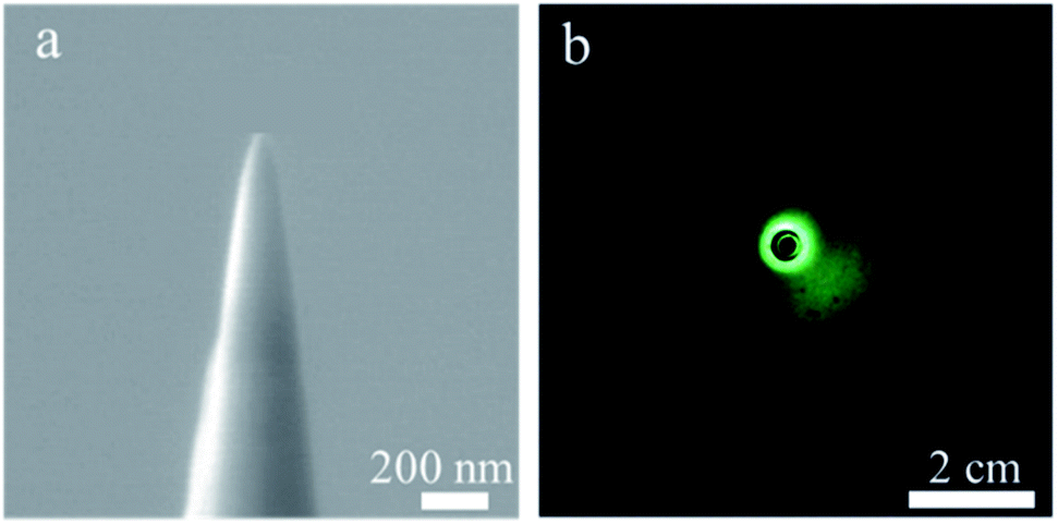 | ||
| Fig. 1 (a) SEM image of a finished LaB6 nanoneedle as a field emission electron source showing a sharpened tip with a radius of curvature of 11 nm. (b) Field emission image of the LaB6 nanoneedle with a single emission spot in the axial direction. It should be noted that there is a hole at the centre of the microchannel plate for measurement of probe current. | ||
Field emission characteristics and current stability
To assess the field emission properties, Fig. 2a shows the emission current (I) versus extraction voltage (V). It follows the Fowler–Nordheim equation as expressed in the following form | (1) |
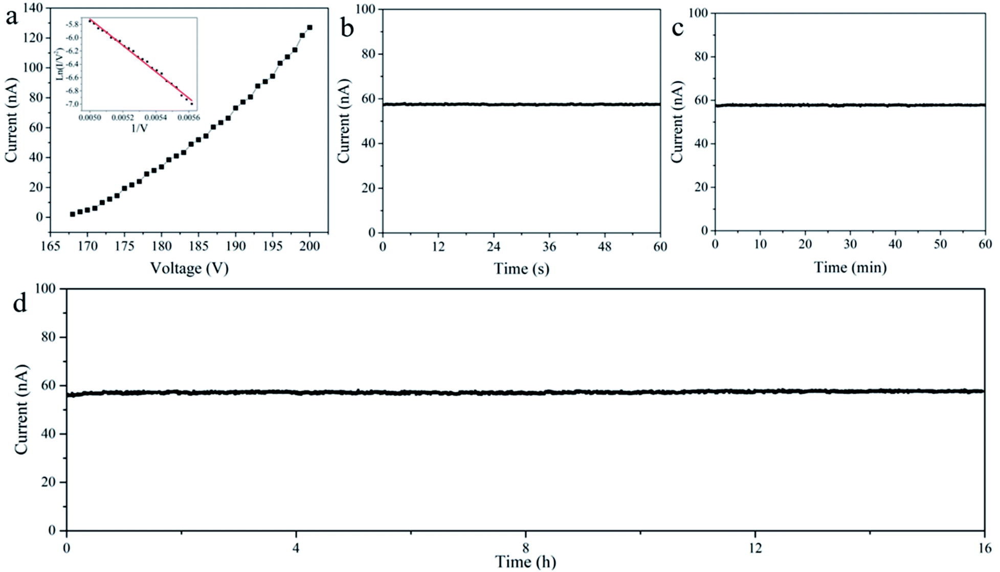 | ||
| Fig. 2 (a) I–V plot with error bars showing excellent agreement with the F–N theory. The inset is a linearized F–N plot with a residual of R2 = 0.993. (b) Short-term stability with a fluctuation of 0.2% in a period of 60 seconds. (c) Medium-term stability with a fluctuation of 0.3% in a period of 60 min. (d) Long-term stability with a fluctuation of 0.7% in 16 hours of measurement. | ||
The energy spread is estimated from the full width at half maximum (FWHM) of the total energy distribution.35 In this particular example, a narrow energy spread of 0.2 eV was obtained by calculation (Experimental section). It is much smaller than that of W(310) which is 0.4 eV due to its greater work function (4.3 eV).36
As described earlier, the emission stability is of crucial importance for the field emission filament in practical operations. For the W(310) field emission filament, apart from its having a large work function of 4.3 eV, a major shortcoming has been that its field emission is unstable and degrades rapidly, so an extreme high vacuum (EHV, ∼10−9 Pa or higher) has to be used in order to extract a usable emission current and reduce current degradation. This stringent requirement has imposed great challenges for practical applications. Fig. 2a–d show the measurements of emission stability of the LaB6 nanoneedle acquired in a vacuum of 1 × 10⁻⁷ Pa at an emission current of 57 nA. To demonstrate the stability of emission, we performed analyses of short-term (60 seconds), medium-term (60 minutes), and long-term (16 hours) measurements. The current stability, calculated as 〈ΔI2〉1/2/〈I〉, where I is the emission current and ΔI is the variation of current, was 0.2%, 0.3%, and 0.7%, respectively. On the other hand, when the emission current was increased to 104 nA, in the same vacuum, the emission current fluctuations also increased slightly, as expected, though they were still below 0.5% and 1.5% for continuous measurement over 60 minutes and 8 hours, respectively. However, it should also be noted that this structure had been continuously active in field emission for more than 500 hours and it showed stable emission without decay.
Current decay and current noise of LaB6 nanoneedle emitter
To illustrate the improvement in the field emission stability of the LaB6 nanoneedle, a comparison of the current decay and emission noise between the LaB6 nanoneedle and W(310) is given in Fig. 3. For the W(310) emitter, the current decreased to 80% in 10 hours while the LaB6 nanoneedle emitter showed no current decay (Fig. 3a).37 The emission noise, defined as (Imax − Imin)/Iavg in the first min of every hour, was also compared. For the W(310) emitter, the emission noise increased rapidly with the emission time from 1.1% (first hour) to 18.5% (9th hour), while the noise for the LaB6 nanoneedle was stable at 1–2% even after 10 hours of continuous emission (Fig. 3b).33 It should also be noted that the W(310) emission was operated at an EHV of 10−9 Pa while the LaB6 nanoneedle was operated at an ultrahigh vacuum (UHV) of 10−7 Pa. We expect the LaB6 nanoneedle to show even more stable emissions when it is operated in an EHV of 10−9 Pa.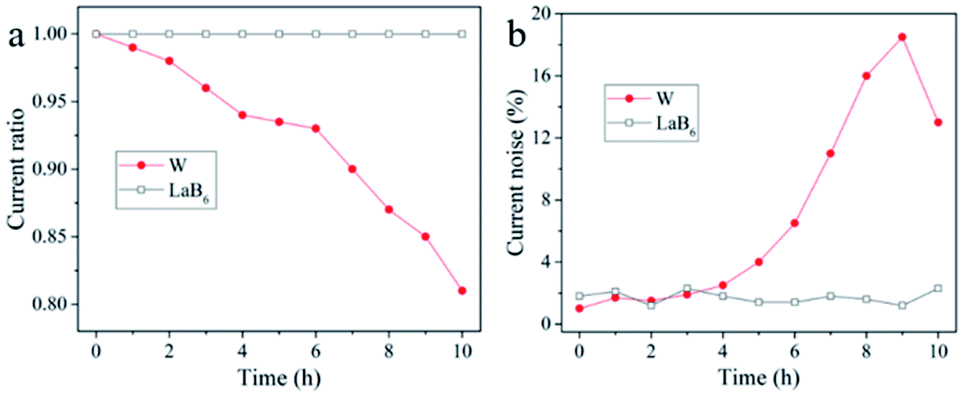 | ||
| Fig. 3 Comparison of current decay and noise between the LaB6 nanoneedle and W(310) cold field emission sources.37 (a) Current decay vs. emission time. The emission current of W (310) decreased to 80% after 10 hours, while the emission current of the LaB6 nanoneedle showed no decay. (b) Current noise vs. emission time. The noise is calculated by (Imax − Imin)/Iave in the first minute of every hour. The noise of W(310) increased with emission time and the its maximum is 18.5%, while the noise of the LaB6 nanoneedle is stable with noise at 1–2%.33 | ||
The recovery and reproducibility of stable emission current after exposure to air are also essential for practical applications and this has been verified by experimental measurements using a controlled procedure. The emitter still showed a fluctuation of 1% per hour after it was exposed to air for two weeks.
In brief, the LaB6 nanoneedle generated a field emission electron beam of higher brightness, greater stability, and smaller energy spread. It can be operated in a vacuum of 10−7 Pa.
Structural characterization of LaB6 nanoneedle
To illustrate the structural features of the LaB6 nanoneedle that enabled its excellent performance in field emission, Fig. 4a shows a TEM image of the LaB6 nanoneedle after field emission measurements. The tip remained sharp and retained its crystalline structure as shown in the selected-area electron diffraction pattern. Fig. 4b shows a high-resolution TEM (HRTEM) image revealing clearly the (100) and (110) lattice fringes of LaB6 with lattice spacings of 0.42 nm and 0.29 nm, respectively. No noticeable mechanical vibration was observed during the TEM examinations, in sharp contrast to the vibrations of the suspended LaB6 nanowire emitter.26 To examine the chemical compositions of the finished nanoneedle tip, energy-dispersive X-ray spectroscopic (EDS) mapping was conducted. The La and B atoms came from the main body of LaB6, Ga was implanted during FIB milling, and O is attributed to surface oxidation after exposure to air. It should be noted that, before field emission was activated, a thermal flashing pre-treatment was carried out to remove the surface oxidation layer to obtain a fresh LaB6 surface.38 To reveal further details of the nanostructure of the LaB6 nanoneedle, line profiles of EDS from the tip region were recorded as shown in Fig. 4g and h. The depth profiles reveal the compositional variations, from which we observed clearly that the concentration of La is uniform at the surface while the concentration of B increases gradually from the surface to the interior and becomes saturated at a depth of 10 nm. This result showed that the ratio of La/B (∼1/3) on the surface is larger than the typical ratio of 1/6 of LaB6, which is actually beneficial for lowering the work function.28,39 The Ga atoms are distributed uniformly at the surface with a concentration of only 1 at%. The concentration of O atoms decreased gradually and became saturated at a depth of 30 nm. One possible concern is that the various crystallites in different orientations at the tip surface of the nanoneedle may exhibit different work functions. However, the EDS mapping revealed that the La/B ratio on the surface is much greater than 1/6, leading us to suggest that the emitting facet was likely to be La-rich regardless of its orientation. This should also help explain the result that the measured work function is insensitive to the orientation of the emitting facet.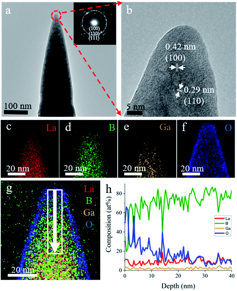 | ||
| Fig. 4 TEM image and EDS analysis after stable field emission. (a) TEM image showing the sharpened LaB6 nanoneedle tip. The inset is a selected-area electron diffraction pattern showing the polycrystalline structure of the nanoneedle tip. (b) HRTEM image showing the tip with a hemispherical apex having a radius of 7.5 nm. Lattice fringes are well resolved showing excellent structural stability free of vibrations. (c–g) EDS maps of the chemical composition and distribution of (c) lanthanum (La), (d) boron (B), (e) gallium (Ga), (f) oxygen (O), and (g) La + B + O + Ga. (h) Depth profiling with concentrations of La, B, Ga, and O along the arrow shown in (g). | ||
For such a sharpened tip with a radius of curvature of about 11 nm, when the applied extraction voltage was 185 V, the local electric field at the tip apex is about 2 V nm−1, much lower than that applied to a typical W(310) filament. For application as a point electron source, the reduced electric field benefits two aspects greatly: (i) it could be operated in a relatively lower vacuum and (ii) a modest thermal flashing procedure could recover the emission performance when the filament is contaminated to result in instabilities in electron emission.
For a practically usable electron source, a great issue has been the stability of the emission current. We wish to emphasize that the LaB6 nanoneedle exhibited a surprising emission stability at a practically usable emission probe current of 10 nA without any decay, in contrast to the less than 3 nA for the W single-atom tips with a decay to 90% in 7 hours. We attribute the emission stability to the following factors in comparison with the W filament: (i) to reach the same probe current (∼3 nA), the total emission current for the LaB6 nanoneedle (50 nA) is much smaller than that of the W filament (10 μA), which reduces the possibility of ion bombardment by decreasing the electron-stimulated-desorption of ions from the electrodes and ions generated in vacuum;11,40 (ii) the local field at the LaB6 nanoneedle tip apex is about 50% that on W; the extraction voltage, and therefore the electric field in between the cathode nanoneedle and anode electrode, is much lower, so the ionization of the residual gases in the emission vacuum chamber is greatly reduced;40 (iii) the large emission current density would transfer the electron energy to the surface atoms, making them hop in the direction of electron flow and combine into a gas molecule, which desorbs from the surface and therefore reduces the adsorption/desorption events on the nanoneedle tip apex which are largely responsible for emission instabilities.41,42
Conclusions
The LaB6 nanoneedle point electron source offers a renewed opportunity to overcome the challenges facing the development of field emission point electron sources. Experimental trials in a Cs-corrected transmission electron microscope are expected to produce further confirmation of its electron optical performance owing to its viable structure. The LaB6 nanoneedle field emitter is also expected to lead to a new generation of point electron sources and therefore a new generation of electron microscopes.Experimental
Fabrication of the LaB6 nanoneedle emitter
The LaB6 nanoneedle emitter was fabricated from a bulk LaB6 crystal by a lift-out method using an FIB-SEM dual beam system (FEI Helios 650). The fabrication processes are as follows: (i) a W(310) needle with a radius of 100 nm was cut by a FIB to produce a flat platform at the tip; (ii) a piece of LaB6 was lifted out from the bulk LaB6 crystal and transferred onto the flat platform of the W(310) needle; (iii) FIB milling was performed to sharpen the LaB6 tip with a Ga-ion beam to obtain the designed structure and geometry.Structural characterization
The microstructure and chemical composition of the LaB6 nanoneedle were characterized using a FIB-SEM dual beam system and Cs-corrected transmission electron microscope (FEI Titan 80–200 kV) equipped with an energy-dispersive X-ray spectrometer (EDS).Field emission measurements
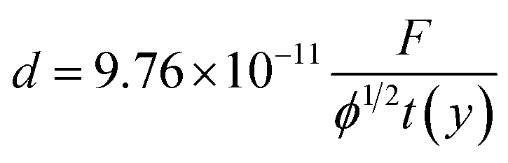
The field emission characteristics were measured in a high vacuum chamber (1 × 10⁻⁷ Pa) with both field emission and thermal flashing functions. Before field emission, a thermal flashing pretreatment was carried out to clean the surface of the LaB6 nanoneedle. During field emission, a negative voltage was applied on the LaB6 nanoneedle emitter to induce electron emission. A grounded annular extractor with a diameter of 1 cm was placed in front of the LaB6 nanoneedle emitter. A grounded microchannel plate (MCP) was placed in front of the LaB6 nanoneedle emitter to observe the field emission pattern. The distance between the emitter and MCP was 5 cm. An electrometer (Keithley 6514) was connected between the power supply and emitter for floating potential measurement of the total current.Calculations of energy spread and reduced brightness
The reduced brightness is expressed as| Br = 1.44J/πd, | (2) |
 | (3) |
The energy spread deduced from the total energy distribution (TED) of electrons due to field-induced emission is35
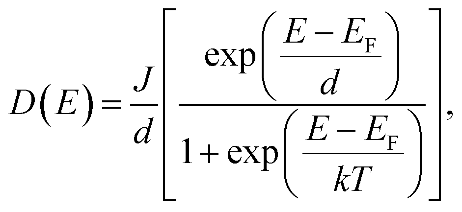 | (4) |
Author contributions
S. T. prepared the samples and carried out structural characterization and field-emission measurements. S. T., J. T. and L. C. Q. analyzed the data and wrote the manuscript. J. U. and T. O. participated in the sample preparation and TEM characterization. W. H., J. Y., M. T. and M. M. participated in data analysis and TEM characterization. J. T. and L. C. Q. conceived the project. J. T. designed and supervised the research. All authors participated in finalizing the manuscript.Conflicts of interest
There are no conflicts to declare.Acknowledgements
This work was supported partially by the NIMS-DENKA Centre of Excellence for Next Generation Materials. A part of this work was also supported by the NIMS Microstructural Characterization Platform as a program of “Nanotechnology Platform” of the Ministry of Education, Culture, Sports, Science and Technology (MEXT), Japan.Notes and references
- M. Knoll and E. Ruska, Z. Phys., 1932, 78, 318 CrossRef CAS.
- H. Rose, Optik, 1990, 85, 19–24 Search PubMed.
- M. Haider, S. Uhlemann, E. Schwan, H. Rose, B. Kabius and K. Urban, Nature, 1998, 392, 768–769 CrossRef CAS.
- P. E. Batson, N. Dellby and O. L. Krivanek, Nature, 2002, 418, 617–620 CrossRef CAS PubMed.
- C. L. Jia, M. Lentzen and K. Urban, Science, 2003, 299, 870–873 CrossRef CAS PubMed.
- K. M. Yip, N. Fischer, E. Paknia, A. Chari and H. Stark, Nature, 2020, 587, 157–161 CrossRef CAS PubMed.
- N. Nakane, et al. , Nature, 2020, 587, 152–156 CrossRef PubMed.
- E. W. Müller, Z. Phys., 1937, 106, 541–550 CrossRef.
- R. H. Fowler and L. Nordheim, Proc. R. Soc. London, Ser. A, 1928, 119, 173–181 CAS.
- N. D. Lang, A. Yacoby and Y. Imry, Phys. Rev. Lett., 1989, 63, 1499 CrossRef CAS PubMed.
- T. Ishikawa, T. Urata, B. Cho, E. Rokuta and C. Oshima, Appl. Phys. Lett., 2007, 90, 143120 CrossRef.
- H. Kuo, I. Hwang, T. Fu, J. Wu, C. Chang and T. Tsong, Nano Lett., 2004, 4, 2379–2382 CrossRef CAS.
- C.-C. Chang, H.-S. Kuo, I.-S. Hwang and T. T. Tsong, Nanotechnology, 2009, 20, 115401 CrossRef PubMed.
- W. A. de Heer, A. Chatelain and D. Ugarte, Science, 1995, 270, 1179–1180 CrossRef CAS.
- Y. Saito, K. Hamaguchi, K. Hata, K. Uchida, Y. Tasaka, F. Ikazaki, M. Yumura, A. Kasuya and Y. Nishina, Nature, 1997, 389, 554–555 CrossRef CAS.
- N. de Jonge, Y. Lamy, K. Schoots and T. Oosterkamp, Nature, 2002, 420, 393–395 CrossRef CAS PubMed.
- G. Zhao, J. Zhang, Q. Zhang, H. Zhang, O. Zhou, L.-C. Qin and J. Tang, Appl. Phys. Lett., 2006, 89, 193113 CrossRef.
- S. Tang, J. Tang, T.-W. Chui, W. Hayami, J. Uzuhashi, T. Ohkubo, F. Uesugi, M. Takeguchi, M. Mitome and L.-C. Qin, Nano Res., 2020, 13, 1620–1626 CrossRef CAS.
- S. Tang, J. Tang, T. Chui, J. Uzuhashi, D. Tang, T. Ohkubo, M. Mitome, F. Uesugi, M. Takeguchi and L.-C. Qin, Nanoscale, 2020, 12, 16770–16774 RSC.
- K. J. Kagarice, G. G. Magera, S. D. Pollard and W. A. Mackie, J. Vac. Sci. Technol., B: Microelectron. Process. Phenom., 2008, 26, 868–871 CrossRef CAS.
- T.-W. Chiu, J. Tang, S. Tang, J. Yuan and L.-C. Qin, Mater. Today Commun., 2020, 25, 101240 CrossRef CAS.
- T.-W. Chiu, J. Tang, S. Tang, W. Hayami, J. Yuan and L.-C. Qin, Appl. Phys. Lett., 2020, 117, 053101 CrossRef CAS.
- H. Zhang, Q. Zhang, G. P. Zhao, J. Tang, O. Zhou and L.-C. Qin, J. Am. Chem. Soc., 2005, 127, 13120–13121 CrossRef CAS PubMed.
- K. Kasuya, T. Kusunoki, T. Hashizume, T. Ohshima, S. Katagiri, Y. Sakai and N. Arai, Appl. Phys. Lett., 2020, 117, 213103 CrossRef CAS.
- T. Kusunoki, T. Hashizume, K. Kasuya and N. Arai, J. Vac. Sci. Technol., B: Microelectron. Process. Phenom., 2021, 39, 013202 CrossRef CAS.
- H. Zhang, J. Tang, J. Yuan, Y. Yamauchi, T. T. Suzuki, N. Shinya, K. Nakajima and L.-C. Qin, Nat. Nanotechnol., 2016, 11, 273–280 CrossRef CAS PubMed.
- H. Zhang, Q. Zhang, J. Tang and L.-C. Qin, J. Am. Chem. Soc., 2005, 127, 2862–2863 CrossRef CAS PubMed.
- H. Zhang, Q. Zhang, J. Tang, O. Zhou and L.-C. Qin, Adv. Mater., 2006, 18, 87–91 CrossRef CAS.
- M. Futamoto, S. Hosoki, H. Okano and U. Kawabe, J. Appl. Phys., 1977, 48, 3541–3546 CrossRef CAS.
- R. Shimizu, Y. Kataoka, T. Tanaka and S. Kawai, Jpn. J. Appl. Phys., 1975, 14, 1089 CrossRef CAS.
- L. W. Swanson, M. A. Gesley and P. R. Davis, Surf. Sci., 1981, 107, 263–289 CrossRef CAS.
- G. Singh, R. Bücker, G. Kassier, M. Barthelmess, F. S. Zheng, V. Migunov, M. Kruth, R. E. Dunin-Borkowski, S. T. Purcell and R. J. Dwayne Miller, Appl. Phys. Lett., 2018, 113, 093101 CrossRef.
- K. Kasuya, S. Katagiri, T. Ohshima and S. Kokubo, J. Vac. Sci. Technol., B: Microelectron. Process. Phenom., 2010, 28, L55–L60 CrossRef CAS.
- G. A. Schwind, G. Magera and L. W. Swanson, J. Vac. Sci. Technol., B: Microelectron. Process. Phenom., 2006, 24, 2897–2901 CrossRef CAS.
- R. D. Young, Phys. Rev., 1959, 113, 110–114 CrossRef CAS.
- L. W. Swanson and L. C. Crouser, Phys. Rev., 1967, 163, 622 CrossRef CAS.
- H. Sawada, N. Shimura, K. Satoh, E. Okunishi, S. Morishita, T. Sasaki, Y. Jimbo, Y. Kohno, F. Hosokawa, T. Naruse, M. Hamochi, T. Sato, K. Terasaki, T. Suzuki, M. Terao, S. Waki, T. Nakamichi, A. Takano, Y. Kondo and T. Kaneyama, JEOL News, 2014, 49, 51–58 Search PubMed.
- C. Oshima, E. Bannai, T. Tanaka and S. Kawai, J. Appl. Phys., 1977, 48, 3925–3927 CrossRef CAS.
- A. Bellucci, M. Mastellone, M. Girolami, V. Serpente, A. Generosi, B. Paci, A. Mezzi, S. Kaciulis, R. Carducci, R. Polinia, S. Orlando, A. Santagata, A. De Bonis, M. Meucci, L. Mercatelli, E. Sani and D. M. Trucchi, Appl. Surf. Sci., 2020, 513, 145829 CrossRef CAS.
- L. W. Swanson and G. A. Schwind, Adv. Imaging Electron Phys., 2009, 159, 63–100 CAS.
- J. R. Black, IEEE Trans. Electron Devices, 1969, 16, 338–347 CAS.
- P. S. Ho and T. Kwok, Rep. Prog. Phys., 1989, 52, 301–348 CrossRef CAS.
- M. Bronsgeest, J. Barth, L. Swanson and P. Kruit, J. Vac. Sci. Technol., B: Microelectron. Process. Phenom., 2008, 26, 949–955 CrossRef CAS.
| This journal is © The Royal Society of Chemistry 2021 |