
 Open Access Article
 This Open Access Article is licensed under a Creative Commons Attribution-Non Commercial 3.0 Unported Licence
Flexible and transparent memristive synapse based on polyvinylpyrrolidone/N-doped carbon quantum dot nanocomposites for neuromorphic computing†
Tao
Zeng‡
,
Zhi
Yang‡
,
Jiabing
Liang
,
Ya
Lin
*,
Yankun
Cheng
,
Xiaochi
Hu
,
Xiaoning
Zhao
*,
Zhongqiang
Wang
,
Haiyang
Xu
 * and
Yichun
Liu
* and
Yichun
Liu
Key Laboratory for UV Light-Emitting Materials and Technology (Northeast Normal University), Ministry of Education, 5268 Renmin Street, Changchun, P. R. China. E-mail: liny474@nenu.edu.cn; zhaoxn430@nenu.edu.cn; hyxu@nenu.edu.cn
First published on 29th March 2021
Abstract
Memristive devices are widely recognized as promising hardware implementations of neuromorphic computing. Herein, a flexible and transparent memristive synapse based on polyvinylpyrrolidone (PVP)/N-doped carbon quantum dot (NCQD) nanocomposites through regulating the NCQD doping concentration is reported. In situ Kelvin probe force microscopy showed that the trapping/detrapping of space charge can account for the memristive mechanism of the device. Diverse synaptic functions, including excitatory postsynaptic current (EPSC), paired-pulse facilitation (PPF), spike-timing-dependent plasticity (STDP), and the transition from short-term plasticity (STP) to long-term plasticity (LTP), are emulated, enabling the PVP–NCQD hybrid system to be a valuable candidate for the design of novel artificial neural architectures. In addition, the synaptic device showed excellent flexibility against mechanical strain after repeated bending tests. This work provides a new approach to develop flexible and transparent organic artificial synapses for future wearable neuromorphic computing systems.
Introduction
Brain-inspired neuromorphic computing has attracted great attention as innovative technology owing to its ability to perform intelligent and energy-efficient computation.1–3 Electronic synaptic devices are considered to be the key step for hardware implementation of neuromorphic computation. Among these devices, the emerging memristor is considered to be a promising candidate for synaptic emulation owing to its functional and structural resemblance to the biological synapse.4–8 Memristors with conductance states incrementally modulated by an external electric field have demonstrated capability for emulating diverse important synaptic functions observed in biology.9–12 Moreover, the simple metal/resistive switching (RS) layer/metal sandwich structure can contribute to facilitate implementation of high-density neural networks.13–15 In comparison with their inorganic counterparts, organic–inorganic hybrid systems have tremendous advantages in fabrication of memristive synapses owing to their cost-effective, environmentally friendly, and biocompatible properties.16–18 Polymers are usually used as the active matrix, and low-dimensional inorganic materials, including nanodots,19,20 nanotubes,21,22 and nanosheets,23,24 are introduced into the polymer as charge trapping centers to trigger RS. In many cases, organic–inorganic hybrid based memristors exhibit digital-type RS (D-RS) between the low-resistance state (LRS) and high-resistance state (HRS) for memory storage applications. For example, Ding et al. reported a Ti3C2 nanosheet/polyvinylpyrrolidone (PVP) based memristor with configurable multistate nonvolatile memory behavior.25 Liu developed flexible nonvolatile rewritable memory devices based on MoS2–PVP nanocomposites.26 However, analog-type RS (A-RS) with continuous resistance-state variation, which is urgently needed for biorealistic emulation of synaptic functions, has seldom been reported in organic–inorganic hybrid systems. Owing to the ubiquitous charge trapping effects, the RS behavior is primarily associated with the characteristic of the electron-trapping centers. Therefore, searching for suitable nanomaterial-doped polymers is beneficial for guiding development of A-RS based memristive synapses with excellent performance and environmental benignity.As a novel zero-dimensional carbon nanomaterial, nitrogen-doped carbon quantum dots (NCQDs) possess unique properties, such as small sizes, excellent biocompatibility, excellent aqueous solubility, and low toxicity, and they are considered to be promising materials for a number of biological and optoelectronic applications.27–30 Doping CQDs with electron-rich N atoms is considered to be a valid strategy to modulate their intrinsic properties and improve their fluorescent properties and quantum yield.31,32 More importantly, the polar groups and defects on the surface of NCQDs can regulate generation and recombination of electron–hole pairs,33–35 suggesting the potential feasibility of doping polymers with NCQDs to achieve closely biorealistic artificial synapses based on the trapping-assisted hopping effect.
Herein, we report a flexible and transparent organic memristive synapse with A-RS behavior in NCQD–PVP hybrid composite films. By modulating the doped NCQD concentration, the filled trapping centers under high NCQD concentration promote formation of multiple conductive paths (CPs), leading to a gradual change in the device conductivity. Advanced synaptic functions, such as excitatory postsynaptic current (EPSC), paired-pulse facilitation (PPF), spike-timing-dependent plasticity (STDP), and transformation from short-term plasticity (STP) to long-term plasticity (LTP), are efficiently emulated. In addition, the transparent organic memristive synapse on a poly(ethylene terephthalate) (PET) substrate shows excellent flexibility under a bending test, providing a potential approach for development of green electronics and wearable neuromorphic computing systems.
Results and discussion
The NCQDs were prepared by a simple hydrothermal treatment process using citric acid and urea as the carbon and nitrogen source, respectively (Fig. 1(a)). The detailed preparation schemes of the NCQDs are provided in Fig. S1 in the ESI† and the Experimental section. The surface morphology of the as-prepared NCQDs was characterized by transmission electron microscopy (TEM) and atomic force microscopy (AFM). A TEM image (Fig. 1(b)) showed good dispersion of the NCQDs in water owing to their hydrophilic nature. The particle size distribution of the pristine NCQDs was in the range from 2 to 5 nm (inset of Fig. 1(b)), suggesting the uniform size and nearly spherical shape of the NCQDs. The NCQDs had an average size of 3.5 nm (Fig. 1(c)). To analyze the chemical composition, the X-ray photoelectron spectroscopy (XPS) of the NCQDs was performed. The XPS survey scan of the NCQDs is shown in Fig. 1(d), in which the apparent peaks are located at 284.2, 403.3, and 535.1 eV, corresponding to C 1s of sp2 C, N 1s of the doped N, and O 1s of the oxygen-containing functional groups, respectively.31–33 The structure of the NCQDs was further characterized by Fourier transform infrared (FT-IR) spectroscopy (Fig. 1(e)). The absorption bands of the NCQD surface revealed the presence of polar groups, including –OH, C![[double bond, length as m-dash]](https://www.rsc.org/images/entities/char_e001.gif) O, C–N (CN), and –NH.31–33 The emission fluorescence spectrum of the NCQDs is shown in Fig. 1(f), which is consistent with the phenomenon shown in the photograph in Fig. 1(a), that is, the NCQDs showed bright blue fluorescence under 325 nm ultraviolet light.31–33 The ultraviolet-visible absorption spectrum of the synthesized NCQDs is shown in Fig. 1(g), in which the absorption band peak is located in the 250–280 nm region, showing that the main absorption of the NCQDs is in the ultraviolet region.31–33
O, C–N (CN), and –NH.31–33 The emission fluorescence spectrum of the NCQDs is shown in Fig. 1(f), which is consistent with the phenomenon shown in the photograph in Fig. 1(a), that is, the NCQDs showed bright blue fluorescence under 325 nm ultraviolet light.31–33 The ultraviolet-visible absorption spectrum of the synthesized NCQDs is shown in Fig. 1(g), in which the absorption band peak is located in the 250–280 nm region, showing that the main absorption of the NCQDs is in the ultraviolet region.31–33
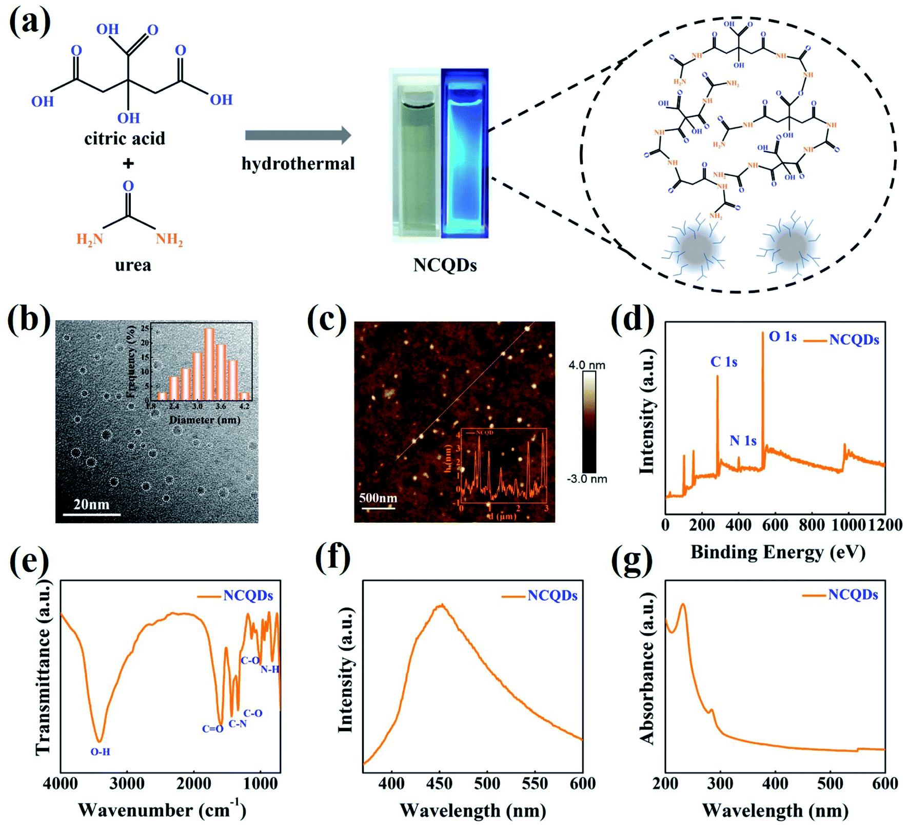 | ||
| Fig. 1 NCQD characteristics. (a) Detailed preparation scheme of the NCQDs. (b) TEM image. (c) AFM image. (d) XPS spectrum. (e) FT-IR spectrum. (f) Fluorescence emission spectrum under 325 nm laser irradiation. (g) Ultraviolet-visible absorption spectrum of the NCQDs on a flexible PET/ITO substrate. | ||
In this work, the NCQDs were inserted into PVP to prepare flexible and transparent artificial synapses. The motivation for developing a highly efficient PVP–NCQD based memristor with biorealistic synaptic functions is shown in Fig. 2(a). The structure and ion transport process of the flexible Al/PVP–NCQD/indium tin oxide (ITO) memristor on a PET substrate are analogous to the ion channel and Ca2+ dynamics of biosynapses. The Al/PVP–NCQD/ITO sandwich structure was prepared in crossbar arrays, as shown in the optical microscope image in Fig. 2(b). In the cross-sectional scanning electron microscopy (SEM) image (Fig. 2(c)), a PVP–NCQD layer with a thickness of 50 nm can be clearly observed between the Al and ITO electrodes, demonstrating the two terminal structure of the device. The surface morphology of the PVP–NCQD film was investigated by AFM (Fig. S2, ESI†). The root mean square roughness value (Rq) was 0.7 nm, confirming the flatness of the as-prepared film. In addition, the PVP–NCQD film was highly transparent, with transmittance of between 90% and 95% in the visible spectrum (Fig. 2(d)). A photograph of the memristive synapse is shown in Fig. 2(e). The device was highly flexible. The data from the mechanical flexibility tests will be discussed later.
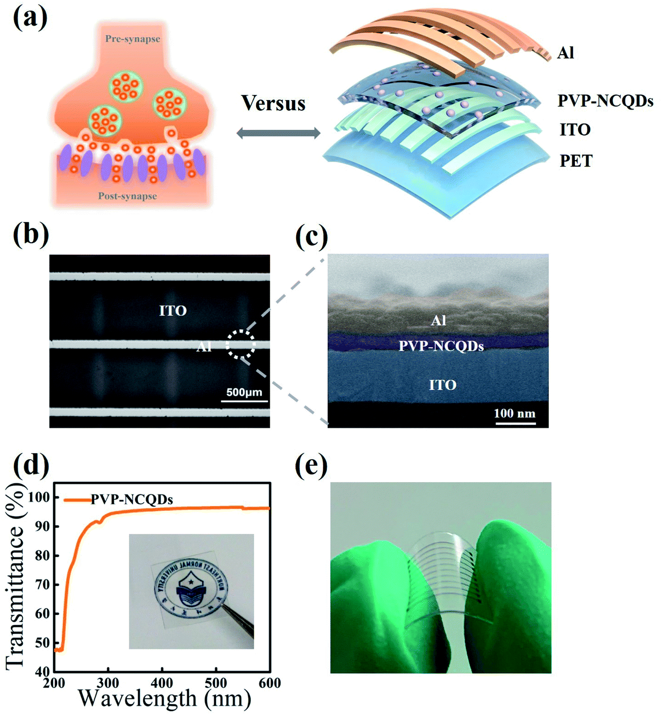 | ||
| Fig. 2 Flexible and transparent Al/PVP–NCQD/ITO memristive synapse. (a) Illustrations of the biological synapse (left) and flexible Al/PVP–NCQD/ITO memristor (right). (b) Optical microscope image of the memristor crossbar array. (c) SEM image of the cross-section of the Al/PVP–NCQD/ITO memristor crossbar array. (d) Ultraviolet-visible transmission spectrum of the PVP–NCQD film. The inset shows a photograph of the transparent memristive synapse. (e) Photograph of the memristive device fabricated on a flexible PET substrate under bending. | ||
To investigate the memristive characteristic of the device, a bias voltage was applied to the Al top electrode and the ITO bottom electrode was grounded. The RS behavior of the device greatly depended on the doping concentration of NCQDs in the nanocomposite. No obvious resistive switching (RS) behavior is appeared in the devices without inserting NCQDs into PVP film beacase there are no charge trapping centers that enhance the localized electric field to aggregate electrons.17,36 (see Fig. S3, ESI†). The typical D-RS behavior after the formation process with a NCQD concentration of 10 wt% is shown in Fig. 3(a), in which an abrupt transition between the HRS and LRS was triggered by a set (0 to 2 V)/reset (0 to −2 V) voltage sweep. The device could be repeatedly switched by 50 consecutive RS cycles (Fig. 3(b)).37,38 When the doping concentration of the NCQDs was increased from 10 to 30 wt% (see Fig. S4, ESI†), both the set and forming voltage greatly decreased, similar to most previous reports.37 It is interesting to note that the transition from D-RS to gradual memristive switching (A-RS) occurred when the doping concentration of the NCQDs was increased from 10 to 40 wt%. Continuous switching of the device (A-RS type) with consecutive positive and negative voltage sweeps (0 to 2 V/0 to −2 V) is shown in Fig. 3(c) and (d), respectively. The insets in Fig. 3(c) and (d) show the variation of the current read at 0.2 V with the cycle number, in which the uptrend (downtrend) is observed after applying positive (negative) sweeps. In addition, the devices with higher concentration exhibit poor A-RS performance duo to the existence of large leakage current in composite film,17,39 suggesting the NCQDs concentration of 40% is the optimal condition to achieve excellent A-RS performance (see Fig. S5, ESI†). Here, to simulate similar information processing to synapses, the memristor was stimulated in the pulse mode. The device conductance continuously strengthened/weakened with 100 consecutive positive/negative voltage pulses (Fig. 3(e) and (f)), which can simulate the synaptic potentiation/depression process when treating the device conductance as the synapse weight.9,10
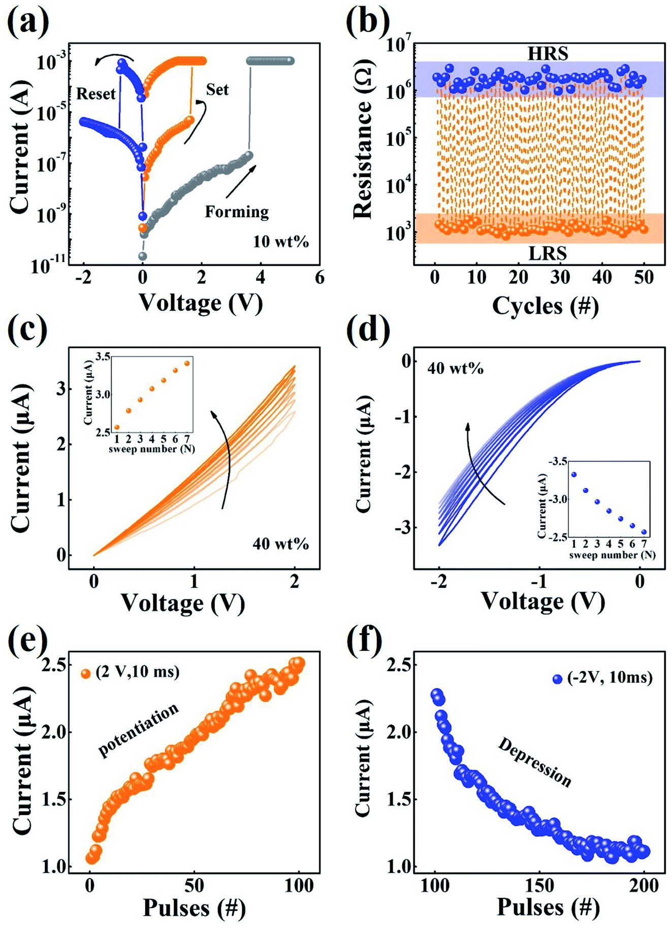 | ||
| Fig. 3 A-RS memristive behavior realized by modulating the doping NCQD concentration in the Al/PVP–NCQD/ITO memristor. (a) I–V characteristics of the memristor with 10 wt% NCQD doping concentration. (b) Statistical values of the HRS/LRS under repeated RS measurement. (c) and (d) I–V characteristics of the memristor with 40 wt% NCQD doping concentration. (e) and (f) Potentiation and depression of the current caused by repeated stimulation of 100 positive pulses (+2 V, 10 ms) and 100 negative pulses (−2 V, 10 ms). | ||
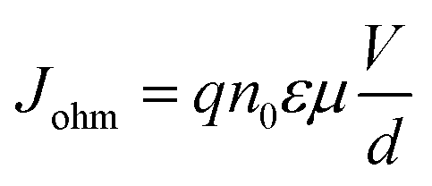
To better understand the conduction mechanism of the devices, the log–log current–voltage (I–V) curves of PVP–NCQD based memristors with different NCQD concentrations (10 and 40 wt%) are shown in Fig. 4(a) and (b). The log–log plot of the direct current sweep exhibited a slope of near one (blue lines) for positive bias in both D-RS and A-RS, indicating typical trap-controlled space-charge limited conduction (SCLC). For the HRS under positive bias, the charge transport behavior consisted of three regions (Fig. 4(a) and (b)). In the low bias region, the transport followed Ohm's law (slope ≈ 1, Johm ∼ V). The J–V equation is as follows:40–42
 | (1) |
 | (2) |
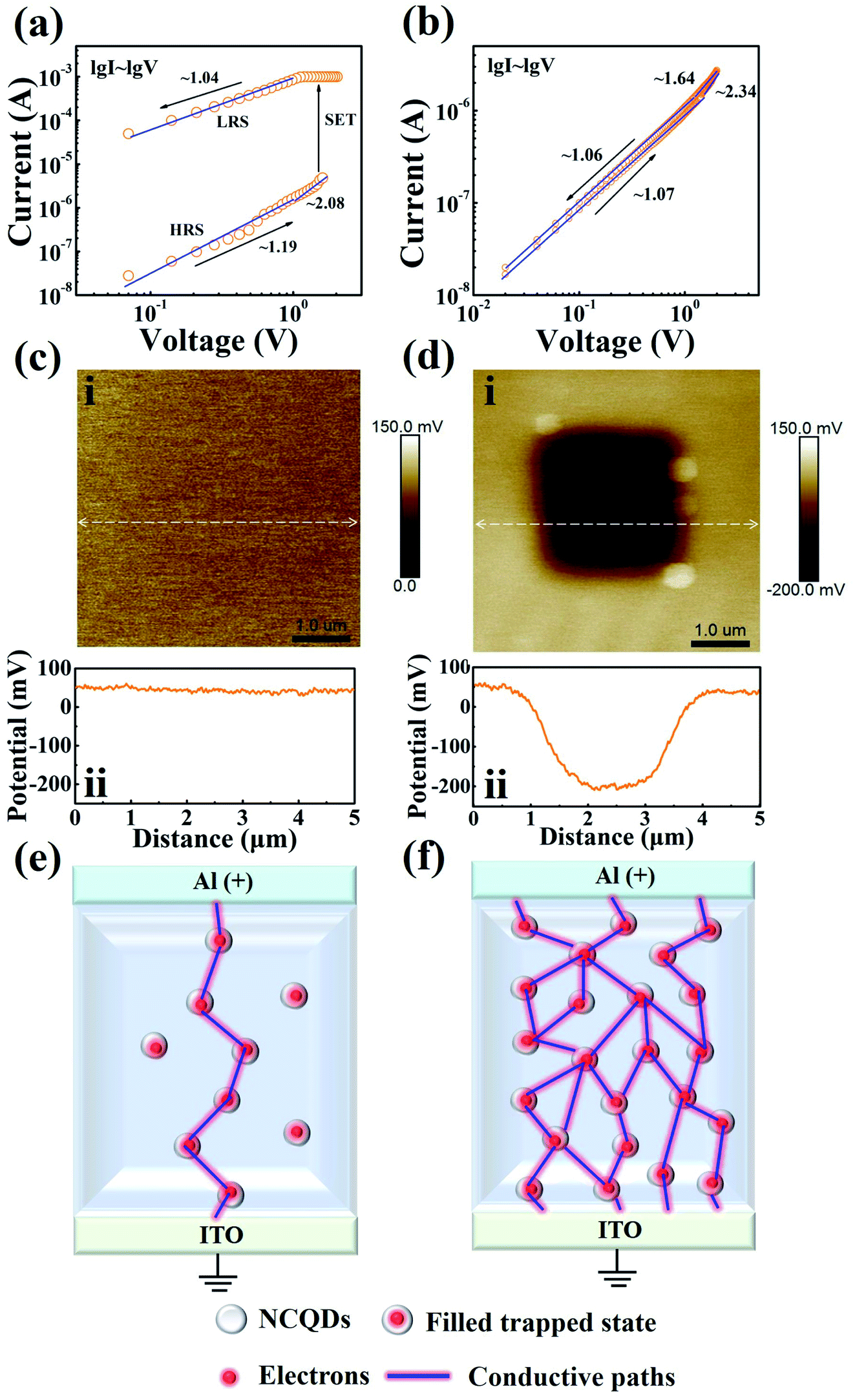 | ||
| Fig. 4 Memristive switching mechanism of D-RS and A-RS in the Al/PVP–NCQD/ITO memristor. (a) and (b) I–V curves in log–log scale in the positive voltage sweeping region of the device with D-RS and A-RS behavior. The charge trapping capability of the PVP–NCQD film was detected by KPFM. Surface potential images of selected cross-sections (c) before and (d) after the charge injection process and the related cross-section data of the surface potential. Schematic diagrams of the mechanisms of (e) D-RS and (f) A-RS. | ||
For the LRS, the conduction mechanism was well fitted by ohmic conduction (slope ≈ 1), which is consistent with formation of a CP in the RS layer. Furthermore, Kelvin probe force microscopy (KPFM) was performed to clearly demonstrate the charge trapping. To form the writing operation for a charge carrier injection process, +5 V tip bias was added to the written square region of about 2 μm × 2 μm (Fig. 4(c)i and (d)i). For surface potential measurement, a 5 μm × 5 μm area was then measured by KPFM. The section data of the surface potential were collected and plotted before and after the charge injection process (Fig. 4(c)ii and (d)ii). The potential difference between the electrical writing region and nonwriting region was ∼250 mV. The potential in the writing region was clearly lower than that in the non-operation region, demonstrating trapping of electrons in the composite films.42,43
One possible switching model is proposed based on the above results (Fig. 4(e) and (f)). The mechanism of RS can be described by a charge trapping assisted hopping conduction model. For the D-RS of the low NCQD concentration (10 wt%) in Fig. 4(e), the charge carriers are injected from the ITO electrode and trapped in the NCQDs under positive bias. Owing to low NCQD concentration, formation of one dominant CP inside the PVP–NCQD nanocomposites resulted in transition from the HRS to the LRS. For the device with high NCQD concentration (40 wt%) in Fig. 4(f), the filled trapping centers under high NCQD concentration tended to form multiple CPs owing to abundant and concentrated trapped defects. The device conductance can be continuously adjusted by controlling the number of these multiple CPs, which is similar to a model involving modulation of the number of CPs leading to a gradual change of the device conductivity of multiple CPs.17,42,43
Such A-RS behavior in the PVP–NCQD based memristor enabled close emulation of synaptic learning functions. The current response of the memristive device under a single spike (2 V, 1 μs) is shown in Fig. 5(a). The single spike triggered an abrupt increase in the current followed by decay to the initial state, which is similar to the excitatory postsynaptic current (EPSC) of the biological synapse.10,44,45 Importantly, the EPSC opens the temporal range for relating the next spike. One typical correlation between spikes is the paired-pulse facilitation (PPF) function, which represents the temporal correlation between two neighboring spikes and is related to the Ca2+ dynamics in biology.46,47 Herein, PPF behavior that continuously enhanced the EPSC by using two successive spikes (2 V, 1 μs) was achieved in the A-RS memristor, as shown in Fig. 5(b). The peak value of the EPSC induced by the second spike I2 was higher than that of the first spike I1, resulting in the PPF effect. The PPF effect weakened with increasing interval time, as shown in Fig. 5(c).
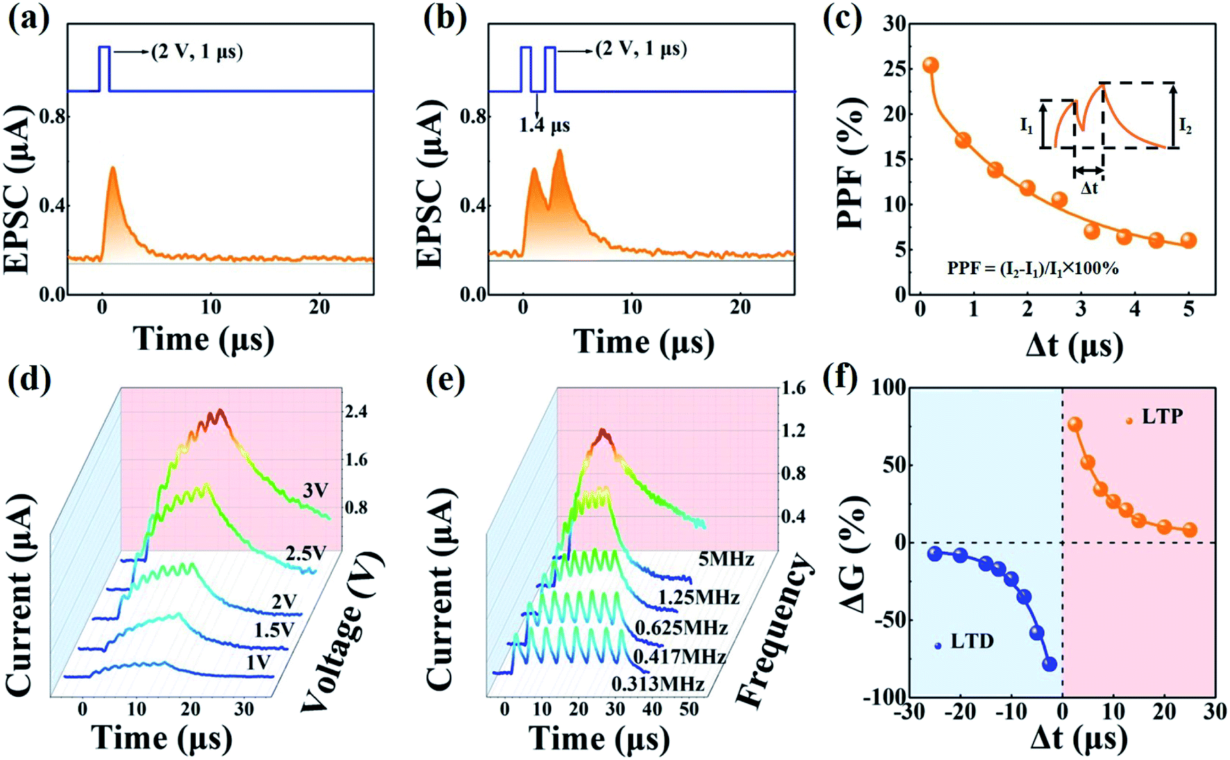 | ||
| Fig. 5 Synaptic learning functions closely emulated in the Al/PVP–NCQD/ITO memristor. Short-term synaptic functions of (a) EPSC, (b) PPF, and (c) PPF versus the relative spike timing. A transition from STP to LTP appears through the (d) pulse amplitude and (e) pulse frequency. (f) Relative changes of the synaptic weight (ΔG) with spike timing (Δt), showing the typical STDP function of the memristive synapses. | ||
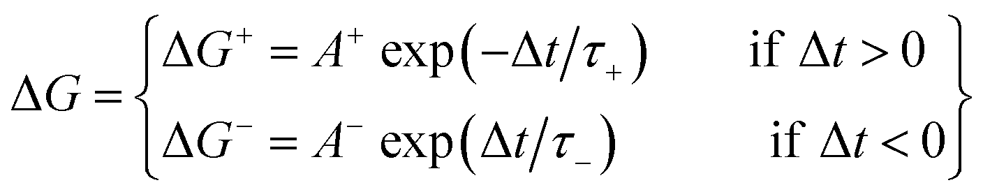
Generally, synaptic plasticity can be divided into short-term plasticity (STP) and long-term plasticity (LTP) depending on the memory retention.9,48 LTP is activated by a permanent change in the synaptic weight. It is believed to be the synaptic mechanism of learning and memory storage, and a transition from STP to LTP appears through repeated rehearsal events.9,48 To measure such a transition, pulses with different amplitudes (1–3 V) were applied to the device. Memory retention was enhanced with increasing pulse amplitude (Fig. 5(d)), demonstrating the transition from STP to LTP. Similarly, memory retention was also enhanced when the pulse frequency was increased from 0.313 to 5 MHz (or the pulse width was increased from 0.2 to 5 μs) (Fig. 5(e) and S6, ESI†). In neuromorphic systems, the spike-timing-dependent plasticity (STDP) learning rules are one typical type of LTP, which is one of the essential learning laws for emulating synaptic functions.49,50 By adjusting the timing between the pre- and postsynaptic spikes, the synaptic weight can be modulated in two ways. To induce LTP, the presynaptic spike needs to precede the postsynaptic spike (Δt > 0), whereas the opposite timing of the pre- and postsynaptic spikes (Δt < 0) induces LTD. To biorealistically implement STDP, a pair of temporally correlated spikes was applied to the top electrode and bottom electrode of the memristor as pre- and postsynaptic spikes, respectively (see Fig. S7 in the ESI† for the detailed trigger signal design). The synaptic weight (ΔG) plotted against the relative timing (Δt) is shown in Fig. 5(f). The change of conductance ΔG as a function of Δt can be expressed by the exponential fitting equation:9,10,49,50
 | (3) |
The PVP–NCQD based memristive synapse also possesses the feature of flexibility for future wearable applications owing to the organic polymer RS layer. To verify the flexibility feature, the Al/PVP–NCQD/ITO device was prepared on PET. A continuous bending test was then performed using a force gauge (Mark-10) and a highly configurable motorized stand (ESM303) (the bending equipment is shown in Fig. S8†). Fifty consecutive positive/negative pulses (2 V/−2 V, 10 ms) were applied to the bent synaptic device. The statistical values of Gmax/Gmin of potentiation/depression under different bending numbers (0–250 times) are shown in Fig. 6(a) and (b). There was no significant change in the potentiation/depression behavior with the number of bending cycles, other than acceptable switching fluctuation, suggesting that the memristive device possessed excellent flexibility against mechanical strain. The above results demonstrated that no obvious degradation was induced by mechanical bending, indicating the excellent bending stability of the device and potential application to flexible and wearable electronics.
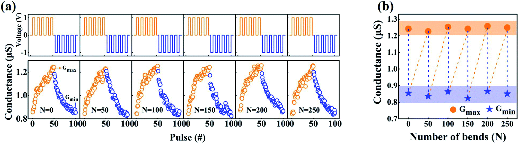 | ||
| Fig. 6 Flexibility characteristic of the Al/PVP–NCQD/ITO synaptic device. (a) Pulse trains (50 positive and 50 negative pulses, 2 V, 10 ms) applied to the device after different bending numbers N. (b) Statistical values of Gmax/Gmin under different bending numbers. | ||
Conclusion
We have experimentally demonstrated a flexible and transparent memristive synapse by inserting NCQDs into PVP. By regulating the NCQD doping concentration, the memristive behavior changes from D-RS to A-RS. The gradual memristive switching is attributed to trapping/detrapping of space charges and formation/rupture of multiple CPs, which is verified by in situ KPFM. Several essential synaptic functions, such as EPSC, PPF, STDP, and a transition from STP to LTP, were demonstrated in the device. In addition, the memristive device can be prepared on a flexible substrate, endowing it with excellent flexibility. This work provides a feasible method for enabling organic memristors to closely simulate synapses, which will broaden the scope for integrating neuromorphic computing systems with novel environmentally friendly and flexible features.Experimental
Preparation of the NCQDs
The NCQDs were synthesized by the hydrothermal treatment method using citric acid and urea. Citric acid (1.4 g) and urea (1 g) were ultrasonically dissolved in 40 mL of secondary deionized water to form a transparent solution. The mixture solution was then transferred to a high-pressure reactor at 180 °C for 5 h with polytetrafluoroethylene as the substrate. The reactant was naturally cooled to room temperature to give a clear brown solution. A dialysis bag with a molecular weight cut-off of 3500 Da was then used to dialyze the solution for 12 h. Finally, NCQD powder was obtained after freeze drying.Device fabrication
Before fabrication of the device, the amount of NCQDs was varied to control the NCQD doping concentration. PVP (1.5 mg) and 0.17, 0.38, 0.64, and 1 mg NCQDs were mixed in 5 mL of secondary deionized water after stirring at room temperature for 2 h to achieve 10, 20, 30, and 40 wt% NCQD doping concentration, respectively. The Al/PVP–NCQD/ITO devices were fabricated on flexible PET substrates and patterned into a crossbar array with a junction area of 100 μm × 100 μm using a metal mask. A 180 nm-thick ITO bottom electrode was prepared by radio frequency sputtering using an ITO target. A PVP–NCQD film with a thickness of 50 nm was spin-coated at room temperature using the prepared solution. An 80 nm-thick Ag top electrode was prepared by electron-beam evaporation.Characterization and electrical measurements
The AFM measurements were performed in air with a Bruker Dimension Icon atomic force microscope (Bruker, Germany). The absorption spectra of the samples were recorded with a UH4150 spectrophotometer. A JEOLJEM 2100F transmission electron microscope was used to characterize the morphology of the NCQDs. A JY HR-800 LabRam Infinity spectrophotometer was used to measure the Raman spectra. The cross-sectional image of the device was recorded by SEM (Nova Nano SEM 450). The X-ray photoelectron Ag spectra were recorded with a Thermo ESCALAB 250 instrument. All of the electrical measurements were performed with a source meter (2636A, Keithley), an arbitrary function generator (3390, Keithley), and an oscilloscope (TDS 2012B, Tektronix). Positive bias voltage was defined as the voltage that produced current flow from the top electrode to the bottom electrode.Conflicts of interest
The authors declare no competing financial interest.Acknowledgements
This work was supported by the fund from Ministry of Science and Technology of China (No. 2018YFE0118300 and 2019YFB2205100), the NSFC for Distinguished Young Scholars (No. 52025022), the NSFC Program (No. 11974072, 52072065, 51732003, 51872043, 51902048, 61774031, 61574031 and U19A2091), the “111” Project (No. B13013), the fund from Ministry of Education of China (No. 6141A02033414), The fund from China Postdoctoral Science Foundation (No. 2019M661185), The Fundamental Research Funds for the Central Universities (No. 2412019QD015) and the Fund from Jilin Province (JJKH20201163KJ).References
- Z. Wang, S. Joshi, S. E. Savel'ev, H. Jiang, R. Midya, P. Lin, M. Hu, N. Ge, J. P. Strachan and Z. Li, Nat. Mater., 2017, 16, 101–108 CrossRef CAS PubMed.
- Y. van de Burgt, E. Lubberman, E. J. Fuller, S. T. Keene, G. C. Faria, S. Agarwal, M. J. Marinella, A. A. Talin and A. Salleo, Nat. Mater., 2017, 16, 414–418 CrossRef CAS PubMed.
- X. Zhu, D. Li, X. Liang and W. D. Lu, Nat. Mater., 2019, 18, 141–148 CrossRef CAS PubMed.
- J. Li, C. Ge, J. Du, C. Wang, G. Yang and K. Jin, Adv. Mater., 2020, 32, 1905764 CrossRef CAS PubMed.
- S. Gao, G. Liu, H. Yang, C. Hu, Q. Chen, G. Gong, W. Xue, X. Yi, J. Shang and R.-W. Li, ACS Nano, 2019, 13, 2634–2642 CAS.
- T. Wang, J. Meng, M. Rao, Z. He, L. Chen, H. Zhu, Q. Sun, S. Ding, W. Bao, P. Zhou and D. Zhang, Nano Lett., 2020, 20, 4111–4120 CrossRef CAS PubMed.
- F. Zhou, Z. Zhou, J. Chen, T. H. Choy, J. Wang, N. Zhang, Z. Lin, S. Yu, J. Kang and H.-S. P. Wong, Nat. Nanotechnol., 2019, 14, 776–782 CrossRef CAS PubMed.
- X. Yan, L. Zhang, H. Chen, X. Li, J. Wang, Q. Liu, C. Lu, J. Chen, H. Wu and P. Zhou, Adv. Funct. Mater., 2018, 28, 1803728 CrossRef.
- Z. Q. Wang, H. Y. Xu, X. H. Li, H. Yu, Y. C. Liu and X. J. Zhu, Adv. Funct. Mater., 2012, 22, 2759–2765 CrossRef CAS.
- Z. Wang, T. Zeng, Y. Ren, Y. Lin, H. Xu, X. Zhao, Y. Liu and D. Ielmini, Nat. Commun., 2020, 11, 1510 CrossRef CAS PubMed.
- Y. Wang, Z. Lv, J. Chen, Z. Wang, Y. Zhou, L. Zhou, X. Chen and S. T. Han, Adv. Mater., 2018, 30, 1802883 CrossRef PubMed.
- J. Zhu, Y. Yang, R. Jia, Z. Liang, W. Zhu, Z. U. Rehman, L. Bao, X. Zhang, Y. Cai and L. Song, Adv. Mater., 2018, 30, 1800195 CrossRef PubMed.
- P. Yao, H. Wu, B. Gao, J. Tang, Q. Zhang, W. Zhang, J. J. Yang and H. Qian, Nature, 2020, 577, 641–646 CrossRef CAS PubMed.
- W. Wang, G. Pedretti, V. Milo, R. Carboni, A. Calderoni, N. Ramaswamy, A. S. Spinelli and D. Ielmini, Sci. Adv., 2018, 4, eaat4752 CrossRef CAS PubMed.
- L. Sun, Y. Zhang, G. Hwang, J. Jiang, D. Kim, Y. A. Eshete, R. Zhao and H. Yang, Nano Lett., 2018, 18, 3229–3234 CrossRef CAS PubMed.
- X. Zhao, H. Xu, Z. Wang, Y. Lin and Y. Liu, InfoMat, 2019, 1, 183–210 CrossRef CAS.
- Y. Lin, Z. Wang, X. Zhang, T. Zeng, L. Bai, Z. Kang, C. Wang, X. Zhao, H. Xu and Y. Liu, NPG Asia Mater., 2020, 12, 64 CrossRef CAS.
- C. Liu, Y.-Q. Cao, D. Wu and A.-D. Li, IEEE Electron Device Lett., 2019, 41, 155–158 Search PubMed.
- S. T. Han, L. Hu, X. Wang, Y. Zhou, Y. J. Zeng, S. Ruan, C. Pan and Z. Peng, Adv. Sci., 2017, 4, 1600435 CrossRef PubMed.
- A. Younis, D. Chu, X. Lin, J. Yi, F. Dang and S. Li, ACS Appl. Mater. Interfaces, 2013, 5, 2249–2254 CrossRef CAS PubMed.
- D. Chaudhary, S. Munjal, N. Khare and V. Vankar, Carbon, 2018, 130, 553–558 CrossRef CAS.
- S. K. Hwang, J. M. Lee, S. Kim, J. S. Park, H. I. Park, C. W. Ahn, K. J. Lee, T. Lee and S. O. Kim, Nano Lett., 2012, 12, 2217–2221 CrossRef CAS PubMed.
- J. Hou, B. Zhang, D. Li, Y. Fu, G. Liu and Y. Chen, J. Mater. Chem. C, 2019, 7, 14664–14671 RSC.
- P. Zhang, C. Gao, B. Xu, L. Qi, C. Jiang, M. Gao and D. Xue, Small, 2016, 12, 2077–2084 CrossRef CAS PubMed.
- G. Ding, K. Zeng, K. Zhou, Z. Li, Y. Zhou, Y. Zhai, L. Zhou, X. Chen and S.-T. Han, Nanoscale, 2019, 11, 7102–7110 RSC.
- J. Liu, Z. Zeng, X. Cao, G. Lu, L. H. Wang, Q. L. Fan, W. Huang and H. Zhang, Small, 2012, 8, 3517–3522 CrossRef CAS PubMed.
- R. Zhang and W. Chen, Biosens. Bioelectron., 2014, 55, 83–90 CrossRef CAS PubMed.
- X. Wu, B. Zhao, J. Zhang, H. Xu, K. Xu and G. Chen, J. Phys. Chem. C, 2019, 123, 25570–25578 CrossRef CAS.
- X. Li, M. Rui, J. Song, Z. Shen and H. Zeng, Adv. Funct. Mater., 2015, 25, 4929–4947 CrossRef CAS.
- L. Wang and H. S. Zhou, Anal. Chem., 2014, 86, 8902–8905 CrossRef CAS PubMed.
- M. Abdullah Issa, Z. Z. Abidin, S. Sobri, S. Rashid, M. Adzir Mahdi, N. Azowa Ibrahim and M. Y. Pudza, Nanomaterials, 2019, 9, 1500 CrossRef PubMed.
- L. Bu, T. Luo, H. Peng, L. Li, D. Long, J. Peng and J. Huang, Microchim. Acta, 2019, 186, 675 CrossRef CAS PubMed.
- Y. Li, Y. Zhao, H. Cheng, Y. Hu, G. Shi, L. Dai and L. Qu, J. Am. Chem. Soc., 2012, 134, 15–18 CrossRef CAS PubMed.
- J. Yu, C. Xu, Z. Tian, Y. Lin and Z. Shi, New J. Chem., 2016, 40, 2083–2088 RSC.
- Z. Qian, J. Ma, X. Shan, H. Feng, L. Shao and J. Chen, Chem.–Eur. J., 2014, 20, 2254–2263 CrossRef CAS PubMed.
- X. Yan, Y. Pei, H. Chen, J. Zhao, Z. Zhou, H. Wang, L. Zhang, J. Wang, X. Li, C. Qin, G. Wang, Z. Xiao, Q. Zhao, K. Wang, H. Li, D. Ren, Q. Liu, H. Zhou, J. Chen and P. Zhou, Adv. Mater., 2019, 31, 1805284 CrossRef PubMed.
- Y. Lin, X. Zhang, X. Shan, T. Zeng, X. Zhao, Z. Wang, Z. Kang, H. Xu and Y. Liu, J. Mater. Chem. C, 2020, 8, 14789–14795 RSC.
- Y. Lin, C. Wang, Y. Ren, Z. Wang, H. Xu, X. Zhao, J. Ma and Y. Liu, Small Methods, 2019, 3, 1900160 CrossRef CAS.
- X. Yan, Q. Zhao, A. Chen, J. Zhao, Z. Zhou, J. Wang, H. Wang, L. Zhang, X. Li, Z. Xiao, K. Wang, C. Qin, G. Wang, Y. Pei, H. Li, D. Ren, J. Chen and Q. Liu, Small, 2019, 15, 1901423 CrossRef PubMed.
- W. Wang, J. Xu, H. Ma, X. Zhao, Y. Lin, C. Zhang, Z. Wang, H. Xu and Y. Liu, ACS Appl. Nano Mater., 2018, 2, 307–314 CrossRef.
- K. Shi, Z. Wang, H. Xu, Z. Xu, X. Zhang, X. Zhao, W. Liu, G. Yang and Y. Liu, IEEE Electron Device Lett., 2018, 39, 488–491 CAS.
- S. R. Zhang, L. Zhou, J. Y. Mao, Y. Ren, J. Q. Yang, G. H. Yang, X. Zhu, S. T. Han, V. A. Roy and Y. Zhou, Adv. Mater. Technol., 2019, 4, 1800342 CrossRef.
- Z. Lv, Y. Wang, Z. Chen, L. Sun, J. Wang, M. Chen, Z. Xu, Q. Liao, L. Zhou and X. Chen, Adv. Sci., 2018, 5, 1800714 CrossRef PubMed.
- L.-G. Wu, J. G. G. Borst and B. Sakmann, Proc. Natl. Acad. Sci. U. S. A., 1998, 95, 4720–4725 CrossRef CAS PubMed.
- P. A. Salin, M. Scanziani, R. C. Malenka and R. A. Nicoll, Proc. Natl. Acad. Sci. U. S. A., 1996, 93, 13304–13309 CrossRef CAS PubMed.
- M. Blatow, A. Caputi, N. Burnashev, H. Monyer and A. Rozov, Neuron, 2003, 38, 79–88 CrossRef CAS PubMed.
- R. Creager, T. Dunwiddie and G. Lynch, J. Physiol., 1980, 299, 409–424 CrossRef CAS PubMed.
- X. Shan, Z. Wang, Y. Lin, T. Zeng, X. Zhao, H. Xu and Y. Liu, Adv. Electron. Mater., 2020, 6, 2000536 CrossRef CAS.
- G. H. Seol, J. Ziburkus, S. Huang, L. Song, I. T. Kim, K. Takamiya, R. L. Huganir, H.-K. Lee and A. Kirkwood, Neuron, 2007, 55, 919–929 CrossRef CAS PubMed.
- G. M. Wittenberg and S. S.-H. Wang, J. Neurosci., 2006, 26, 6610–6617 CrossRef CAS PubMed.
Footnotes |
| † Electronic supplementary information (ESI) available. See DOI: 10.1039/d1na00152c |
| ‡ T. Zeng and Z. Yang contributed equally to this work. |
| This journal is © The Royal Society of Chemistry 2021 |