
 Open Access Article
 This Open Access Article is licensed under a Creative Commons Attribution-Non Commercial 3.0 Unported Licence
Perpendicularly magnetized Co/Pd-based magneto-resistive heterostructures on flexible substrates†
M.
Hassan
 ac,
S.
Laureti
a,
C.
Rinaldi
b,
F.
Fagiani
b,
S.
Varotto
b,
G.
Barucca
c,
N. Y.
Schmidt
d,
G.
Varvaro
*a and
M.
Albrecht
d
ac,
S.
Laureti
a,
C.
Rinaldi
b,
F.
Fagiani
b,
S.
Varotto
b,
G.
Barucca
c,
N. Y.
Schmidt
d,
G.
Varvaro
*a and
M.
Albrecht
d
aConsiglio Nazionale delle Ricerche, Istituto di Struttura della Materia, nM2-Lab, Via Salaria km 29.300, Monterotondo Scalo (Roma), 00015, Italy. E-mail: gaspare.varvaro@ism.cnr.it
bPolitecnico di Milano, Department of Physics and IFN-CNR, via G. Colombo 81, 20133 Milano, Italy
cUniversità Politecnica delle Marche, Dipartimento SIMAU, Via Brecce Bianche, Ancona 60131, Italy
dUniversity of Augsburg, Institute of Physics, Universitätsstraße 1 Nord, D-86159 Augsburg, Germany
First published on 9th April 2021
Abstract
Flexible magneto-resistive heterostructures have received a great deal of attention over the past few years as they allow for new product paradigms that are not possible with conventional rigid substrates. While the progress and development of systems with longitudinal magnetic anisotropy on non-planar substrates has been remarkable, flexible magneto-resistive heterostructures with perpendicular magnetic anisotropy (PMA) have never been studied despite the possibility to obtain additional functionality and improved performance. To fill this gap, flexible PMA Co/Pd-based giant magneto-resistive (GMR) spin-valve stacks were prepared by using an innovative transfer-and-bonding strategy exploiting the low adhesion of a gold underlayer to SiOx/Si(100) substrates. The approach allows overcoming the limits of the direct deposition on commonly used polymer substrates, whose high surface roughness and low melting temperature could hinder the growth of complex heterostructures with perpendicular magnetic anisotropy. The obtained PMA flexible spin-valves show a sizeable GMR ratio (∼1.5%), which is not affected by the transfer process, and a high robustness against bending as indicated by the slight change of the magneto-resistive properties upon bending, thus allowing for their integration on curved surfaces and the development of a novel class of advanced devices based on flexible magneto-resistive structures with perpendicular magnetic anisotropy. Besides endowing the family of flexible electronics with PMA magneto-resistive heterostructures, the exploitation of the results might apply to high temperature growth processes and to the fabrication of other functional and flexible multilayer materials engineered at the nanoscale.
1 Introduction
Flexible electronic devices have received a great deal of attention over the past decades due to some key advantages with respect to conventional rigid systems, such as light-weight, flexibility, shapeability, wearability, and low cost.1 All these properties represent the driving force for the ever-growing research in flexible electronics devices, starting with the fabrication of the first flexible solar cell in 1960 (ref. 2) and nowadays showing all their outstanding potentialities in many technological fields including energy, optics, sensors and information storage, among others.3–13 Aiming to widen the domain of flexible electronics, a significant effort has been recently pursued to develop spin-related electronic devices with in-plane magnetic anisotropy on flexible substrates.3,5,14–24 With respect to conventional electronics, spintronic devices exploit electron spin to achieve additional functionality not provided by charge transport. Giant magneto-resistive spin-valves (GMR-SVs) and magnetic tunneling junctions (MTJs) are well-known examples of spintronic elements, which has been largely investigated for the development of advanced devices, including memories and sensors.25 Both the structures consist of two ferromagnetic layers separated by a non-magnetic spacer (metallic – GMR-SVs or insulating – MTJs), in which the electrical resistance depends on the relative orientation of the magnetization in the two magnetic layers.26 While the first generation of such elements relied on thin films with in-plane magnetic anisotropy, large efforts have been recently made to develop perpendicular magnetized spintronic components on rigid substrates featured by an intrinsic and large uniaxial magnetic anisotropy allowing for additional functionality as well as improved performance for data storage/processing technologies and sensors.27–29 To this aim, [Co/X]N multilayers (where X = Pd, Pt or Ni and N the number of repetitions) have been extensively used as building blocks30–36 due to their large perpendicular magnetic anisotropy (PMA) arising at the interface between the layers (105 to 106 J m−3)32,37,38 and the high tunability of the overall magnetic properties through the modulation of layers' thickness and number of repetitions.39 Contrary to that of the free layer, the orientation of the magnetization of the reference electrode must be relatively insensitive to external fields. For this reason, synthetic antiferromagnetic structures, consisting of two ferromagnetic layers separated by a thin non-magnetic spacer (e.g. Ru)40,41 are commonly used as the reference layer. These synthetic antiferromagnetic structures have also recently attracted a great deal of attention for the development of novel and advanced PMA spintronic devices exploiting the movement of domain walls42 or the displacement and the size change of skyrmions (i.e. a topologically-protected solitons).43–45 Albeit the high potential of PMA spintronic devices, no studies are reported, to the best of our knowledge, on flexible magneto-resistive heterostructures with perpendicular magnetic anisotropy. Indeed, the stringent constrains needed to obtain high-quality PMA magneto-resistive thin film multi-stacks, requiring for a fine control of the stack properties at the sub-nanometer level, hinder the direct deposition on the most common flexible polymeric tapes, which are amorphous and generally present a rougher surface and lower melting temperatures with respect to commonly used single-crystal rigid substrates (e.g. Si). As an alternative to the direct deposition on flexible tapes, transfer-and-bonding strategies, where film stacks are firstly deposited on a rigid, thermally stable, crystalline and smooth substrate/layer and then transferred on flexible tapes, might represent an effective pathway.1 This strategy has also the advantage to allow the film stacks to be transferred on arbitrary and also unconventional substrates (e.g. paper), while the main drawback is represented by the low surface coverage generally achieved.In this work, perpendicular magnetized Co/Pd-based GMR spin-valve thin films (GMR-SVs) consisting of a [Co/Pd]N free layer (FL) and a fully compensated [Co/Pd]N/Ru/[Co/Pd]N synthetic antiferromagnetic reference layer (SAF-RL) separated by a Cu spacer, were prepared for the first time on flexible substrates by using an innovative transfer-and-bonding approach exploiting the low adhesion to SiOx/Si(100) substrates of a gold underlayer.46–49 The strategy is expected to be compatible with existing micro/nano-fabrication processes,50,51 thus having a strong impact on the development of novel flexible functional devices. Besides the great interest of such flexible structures for many applications, such as wearable electronics, soft robotics and biomedicine (e.g. in vivo implants), the complexity of the structure, whose properties are strongly affected by the quality of the interfaces, makes such a system a perfect candidate to test and demonstrate the potential of the proposed strategy, which might be easily extended to other functional multilayer materials engineered at the nanoscale, including those whose fabrication process requires high temperature treatments that impedes the direct deposition on flexible tapes.
2 Experimental details
[Pd(0.9)/Co(0.4)]4/Ru(0.4)/[Co(0.4)/Pd(0.9)]3/Co(0.4)/Cu/[Co(0.4)/Pd(0.9)]2/Pd(2.1) GMR-SV stacks (thicknesses in nanometers) with a Cu spacer layer thickness (tCu) of 2 and 3 nm (Fig. 1) were deposited at room temperature by DC magnetron sputtering (BESTEC UHV system). A Ta(10)/Pd(2.1) buffer layer was used to favor the growth of [Co/Pd]N multilayers with a (111) texture, which is required to obtain a large PMA.52,53 A Pd(2.1) capping layer was deposited on top to prevent the FL oxidation. The single layers' thickness and the number of repetitions of the [Co/Pd]N multilayers were selected on the basis of our previous work54 with the aim to ensure (i) a PMA along the full layer stack, (ii) a strong and compensated antiferromagnetic coupling in the SAF structure, and (iii) two stable parallel/antiparallel magnetization configurations in the spin-valve system. A 10 nm thick weakly-adhering Au underlayer46–49 was interposed between the SiOx/Si(100) substrate and the GMR-SV to favour the transfer of the heterostructure on a flexible tape. All samples were sputter-deposited using an Ar pressure of 3.5 μbar. The deposition rates of each material were set to 0.067 nm s−1 (24 W-DC) for Au, 0.03 nm s−1 (40 W-DC) for Ta, 0.04 nm s−1 (26 W-DC) for Pd, 0.025 nm s−1 (52 W-DC) for Co, and 0.03 nm s−1 (48 W-DC) for Ru. After deposition, large area thin film stacks were easily peeled-off and transferred from the substrate to a flexible tape by using a commercial adhesive polyester tape, 3M 396 (Fig. 2). To favor a better adhesion between the film and the tape during the peeling process, a cellulose acetate butyrate-based paint was spread over the surface of the samples. Conventional GMR-SVs were also prepared as reference systems by direct deposition of the film stacks on SiOx/Si(100) substrates under the same experimental conditions.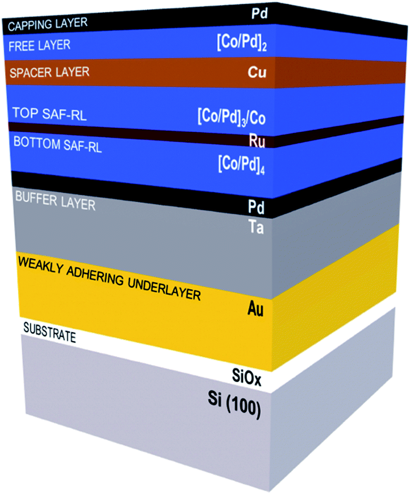 | ||
| Fig. 1 Schematic sample structure of the Co/Pd-based GMR-SV stack consisting of a [Co/Pd]4/Ru/[Co/Pd]3/Co synthetic antiferromagnet reference layer (SAF-RL) and a [Co/Pd]2 free layer separated by a Cu spacer layer. Reference samples were directly deposited on SiOx/Si(100) substrates, while a weakly adhering Au underlayer was interposed to allow for the transfer of the stack on a flexible tape. | ||
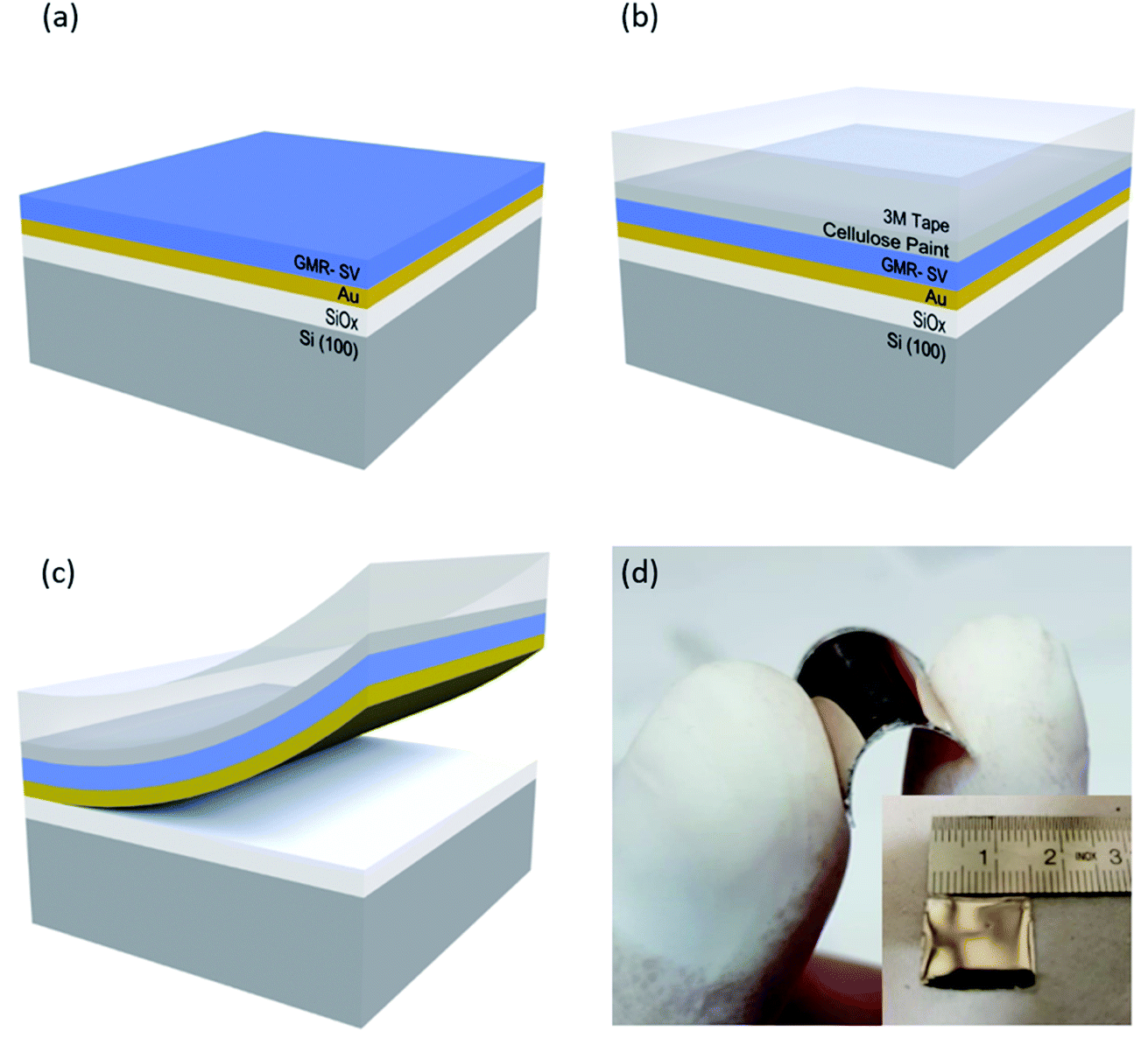 | ||
| Fig. 2 (a–c) Sketch of the Au-mediated transfer-and-bonding approach: (a) perpendicular GMR-SVs are DC sputtered on a SiOx/Si(100) substrate covered with a weakly adhering Au underlayer; (b) a cellulose paint is spread over the film surface to improve the adhesion between the sample and the adhesive tape on which the stack is transferred by a mechanical peel-off step (c). (d) Optical photograph of a flexible perpendicular GMR-SV (tCu = 3 nm). | ||
Room temperature magnetic properties were investigated by using a vibrating sample magnetometer (Model 10 – MicroSense) equipped with a rotating electromagnet that can supply a maximum field of 2 T. Magneto-transport properties were measured at room temperature employing the Van der Pauw method55 on planar, homogeneous square or rectangular samples. Four contacts at the corners of each sample were made on the surface by silver paste and currents in the order of 10 mA flowing in the plane of the films (current-in-plane geometry) were injected using a Keithley 6221 current source, while voltages were measured by a Keithley 2182A nanovoltmeter. Current–voltage characteristics were measured with four different source-measure configurations to compensate for asymmetries and non-idealities using a custom automatic switching board, following the scheme of ref. 56. The homogeneity of our films has been widely tested by comparing different sample sizes and spacing between the four contacts (from 2 × 2 cm down to 2 × 2 mm). The magnetic field was provided by a standard dipole electromagnet (GMW Associates). For measurements under bending conditions, samples were mounted on a semi-cylindrical plastic support with the proper radius of curvature. Transmission electron microscopy (TEM) analysis was performed by means of a Philips CM200 microscope on cross-sectioned films. Owing to the low adhesion between Au and SiOx, an unconventional procedure was developed to obtain thin slices for TEM analysis. GMR-SVs were first glued to a second Si substrate and then peeled-off from the SiOx/Si (100) wafer. This new Si substrate with the GMR-SV firmly attached was glued between two silicon supports to proceed with the standard procedure for TEM cross-section preparation consisting of mechanical polishing by grinding papers, diamond pastes and a dimple grinder. Final thinning was carried out by an ion beam system (Gatan PIPS) using Ar ions at 5 kV.
3 Results and discussion
The room temperature out-of-plane M/Msvs. H loops of GMR-SVs without the Au underlayer (reference samples) are shown in Fig. 3a and b (top panels) as a function of the Cu spacer thickness. A three-step field-dependent magnetization response associated to the individual sharp switching of the top layer of the reference SAF stack (top SAF-RL), the FL and the bottom layer of the reference SAF stack (bottom SAF-RL) is observed in both the samples thus confirming the high reproducibility of the fabrication process, which ensures a large PMA and smooth interfaces to achieve the expected magnetization configuration as a function of the external field. The corresponding magneto-resistance curves (Fig. 3a and b, bottom panels) show the typical behavior expected for a spin-valve system with a SAF reference layer. The change of resistance normalized for its lowest value, ΔR/Rlow = (Rhigh − Rlow)/Rlow, shows a sudden increase in correspondence of the first jump in the hysteresis loop (at ∼0.2 mT) thus indicating that the top SAF-RL switches first. This may be ascribed to a slightly higher magnetic anisotropy of the bottom layer of the SAF that is directly grown on the Pd/Ta buffer layer. The resistance sharply reduces to a low value in correspondence of the magnetization reversal of the FL (at ∼0.15 mT for tCu = 2 nm and ∼0.35 mT for tCu = 3 nm). As the absolute value of the magnetic field increases further, a small kink is observed in the high field region corresponding to the magneto-resistive effect within the SAF-RL. The maximum percentage increase of the resistance, i.e. the GMR ratio of the spin-valve stack, is ∼4.5% for both the samples in line with the data reported in the literature for magneto-resistive systems based on Co/Pd multilayers.57–59 When the film stacks are deposited on the Au-underlayer, the main magnetic and magneto-resistive features are maintained for tCu = 3 nm. The field-dependent magnetization and magneto-resistance loops show the same sharp reversal versus field as in the corresponding reference samples and a still relevant GMR ratio of ∼1.5% (Fig. 3d). However, the M vs. H loop shows an increment of the coercivity of bottom and top layers of SAF (from ∼0.07 T to ∼0.11 T) and a slight reduction of the coercivity of the free-layer (from ∼0.35 mT to ∼0.25 mT), which result in a narrowing of the plateau in the high-resistance region of the MR curves. When the Cu spacer thickness is reduced down to 2 nm, a major change occurs as indicated by the appearance of an “inverted” field-dependent magnetization loop in the region around zero field that also manifests in a significant change of the magnetic–resistance curve (Fig. 3e). This can be attributed to a coupling between the FL and the top SAF-RL as evidenced by the field-dependent resistance loops measured within the low-field region where only the FL switches (from −0.15 to 0.15 mT) reported in Fig. S1 of the ESI.†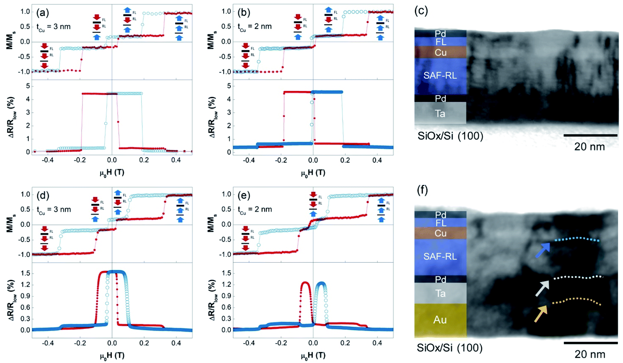 | ||
| Fig. 3 (a, b, d and e) Room temperature out-of-plane field-dependent magnetization loops (M/Msvs. H) and the corresponding magneto-resistance response (ΔR/Rlowvs. H) of perpendicular GMR-SVs deposited on (a and b) SiOx/Si(100) (reference samples) and (d and e) Au/SiOx/Si(100) substrates as a function of Cu spacer thickness: (a and d) tCu = 3 nm, (b and e) tCu = 2 nm. Different colors and symbols are used to evidence the two sweep directions of the external field (ascending red, descending blue). The sketches reported in the top panels denote the mutual alignment of the magnetization (arrows) in the FL, top SAF-RL, and bottom SAF-RL at different points in the loop for the magnetic field sweep from positive to negative values. (c and f) TEM bright field image of GMR-SV stacks (tCu = 3 nm) on (c) SiOx/Si (100) and (f) Au/SiOx/Si (100). In (f) the Volmer–Weber growth mechanism of the Au underlayer results in a wavy interface with the Ta buffer layer (gold arrow and dotted line); the ripple is then transferred to the Pd/SAF-RL (white arrow and dotted line) and the SAF-RL/Cu (blue arrow and dotted line) interfaces. | ||
The observed differences with respect to the reference samples are ascribed to the specific morphology of the Au underlayer, whose growth on SiOx follows the Volmer–Weber mechanism, involving the nucleation and growth of islands that coalesce when the thickness reaches a value between 10 and 15 nm.47 The resulting nanogranular microstructure can lead to surface inhomogeneity extending over the whole structure deposited on top, which may affect the PMA of the Co/Pd multilayers,60,61 the interlayer exchange coupling in synthetic antiferromagnetic heterostructures,62 and the magneto-resistive properties of the whole GMR spin-valve stack.63 To investigate in details the microstructural changes induced by the Au underlayer, TEM analysis was performed on two identical stacks (tCu = 3 nm) with and without Au. Fig. 3c shows a very smooth and sharp interface between the Ta/Pd buffer layer and the SAF obtained by direct deposition on SiOx/Si (100) substrates, which regularity extends over the successive layers. The Cu layer is clearly visible with a uniform thickness of about 3 nm, in perfect agreement with the nominal value. On the contrary, in samples deposited on Au/SiOx/Si(100), the TEM image in Fig. 3f shows the presence of adjacent Au islands, confirming the Volmer–Weber growth resulting in a wavy surface (yellow arrow and dotted line in Fig. 3f and S2 in the ESI†) with an estimated amplitude and wavelength of ∼1.5 nm and ∼20 nm, respectively. Although the roughness tends to be transmitted to the upper layers (white and blue arrows and dotted lines at the buffer layer/SAF and SAF/Cu interfaces in Fig. 3f), the ratio between the amplitude and the wavelength associated to it is small enough that the whole structure is overall retained. However, the presence of this roughness can be a source of inhomogeneity and defects, which in turn may locally affect the magnetic and magneto-resistive properties of the system. In particular, it may be responsible for the reduction of the GMR ratio63 and the enhancement of the coercivity of the bottom and top layers of the SAF as a result of an increase in domain wall pinning.64,65 Moreover, it can be the source of interlayer magnetostatic interactions (orange-peel Néel coupling) or a direct exchange coupling through the formation of pinholes in the Cu spacer layer,63 between the FL and the top SAF-RL, which may explain the inverted magnetization loop for tCu = 2 nm and the slight reduction of the coercivity of the free layer for tCu = 3 nm.
Spin-valve thin film stacks with a Cu spacer thickness of 3 nm, showing the characteristic magnetic and magneto-resistive features of perpendicular magnetized GMR-SVs with a SAF-RL and a still relevant GMR ratio when grown on the Au underlayer, were transferred on a flexible tape by mechanical peel-off (Fig. 2). Despite the presence of very thin layers forming the spinvalve thin film stacks whose thickness is as low as 0.4 nm for Co and Ru, both the magnetic and magneto-resistive behavior remain unchanged after the peeling-off process (Fig. 4), thus demonstrating the high robustness of the system and the high potentiality of the proposed Au-mediated transfer-and-bonding methodology that allows transferring complex multilayered heterostructures on flexible tapes without sacrificing their properties.
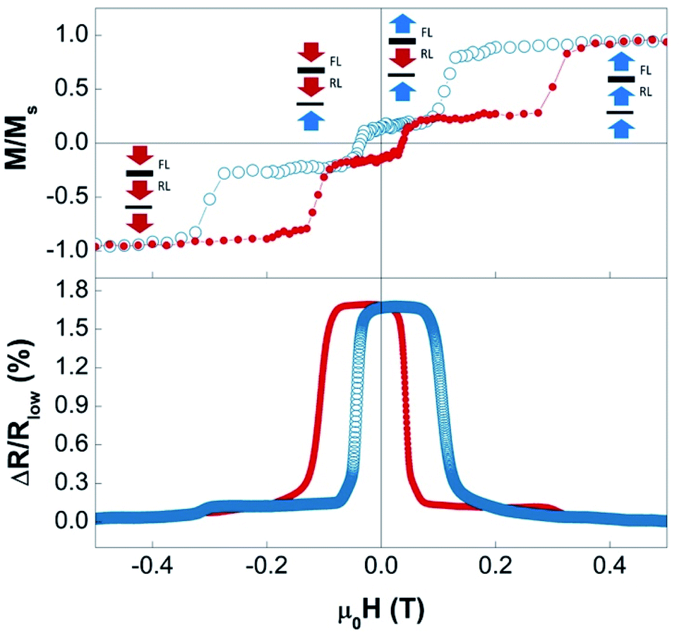 | ||
| Fig. 4 Flexible GMR-SVs (tCu = 3 nm). Room temperature out-of-plane field-dependent magnetization loop (M/Msvs. H) and corresponding magneto-resistive response (ΔR/Rlowvs. H). Different colors and symbols were used for indicating the upward (red) and downward (blue) field sweep direction. The sketches reported in the top panel denote the mutual alignment of the magnetization (arrows) in the FL, top SAF-RL, and bottom SAF-RL at different points in the loop for the magnetic field sweep from positive to negative values. | ||
In order to explore the possibility to integrate such flexible systems on curved surfaces, bending tests under a uniform magnetic field were performed on flexible spin-valves with tCu = 3 nm. To the best of our knowledge, the effect of bending in perpendicular magnetized GMR-SV thin film stacks is not reported in literature and here we disclose the influence of the geometry of a bended heterostructure. When a bended GMR-SV thin film stack with PMA is placed in a uniform magnetic field, each region of the folded sample will experience a different angle with the external magnetic field (Fig. S3 in the ESI†), thus resulting in a variation of the magneto-resistance. To quantify the geometrical effect of a folded heterostructure, samples were glued to a plastic semi-cylindrical support with a given radius of curvature r = 5 mm (Fig. 5a) and Van der Pauw measurements were performed at different bending angles θ (°) = L × 360/2πr ranging between 20° and 180°, where L is the distance between the electrical contacts along the side of the sample parallel to the bending along which the probing current is injected (Fig. S4 in the ESI†). This configuration with a fixed radius of curvature allows measuring the effect of the angular distribution between the magnetic field and the easy-axis while keeping constant the strain to which the heterostructure is subjected. Representative magneto-resistance curves for different bending angles are reported in Fig. 5c and d. As compared to the planar structure, the GMR ratio of the bended samples (hereafter called GMRB (θ), where “B” stands for “bended”) slightly decreases by ∼15% of the GMR of the flat sample for θ = 180°.
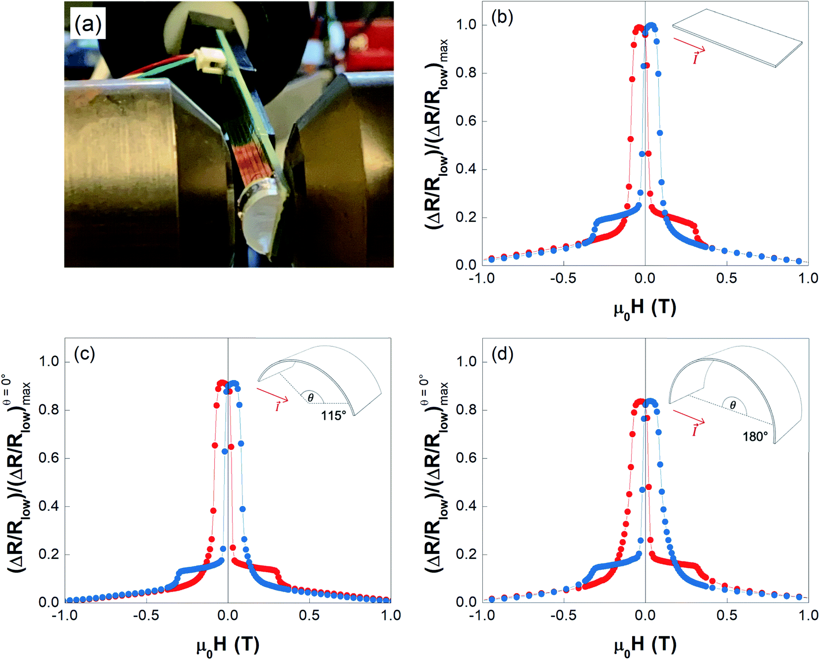 | ||
| Fig. 5 (a) Experimental setup used for magneto-resistive measurements of flexible GMR-SVs with PMA under bending conditions. (b–d) Representative room temperature magneto-resistance curves of flexible perpendicular GMR-SVs with tCu = 3 nm: (b) without bending (θ = 0°) and (c and d) under a bending angle θ of (c) 115° and (d) 180°; the probing current I is injected parallelly to the curvature. Curves are normalized to the maximum ΔR/Rlow value measured on the flat sample (θ = 0°). | ||
To explain the observed behavior, the change of the magnetization loops was studied on planar samples (i.e. without bending) as a function of the angle Φ between the external applied field H and the film normal (Φ = 0° for H perpendicular to the film plane). As shown in Fig. 6a, the characteristic three-step behavior of perpendicular magnetized GMR-SVs with a SAF-RL is retained up to Φ = 45°, while at larger angles (Φ ≥ 60°) the shape of the loop significantly changes with a progressive evolution towards a fully reversible curve at Φ = 90°, corresponding to the magnetic hard-axis of the stack. This magnetic behavior reflects in the magneto-resistance curves measured as a function of the angle Φ (Fig. 6b), revealing that the magneto-resistive response is almost insensitive for angles Φ ≤ 45°. Fig. 6c indicates that the GMRP ratio (where “P” stands for “planar”) slowly decreases with Φ approaching a cross-geometry configuration when the magnetic field is parallel to the sample surface (Φ = 90°), where the magneto-resistance curve significantly differs from that measured at Φ = 0°.
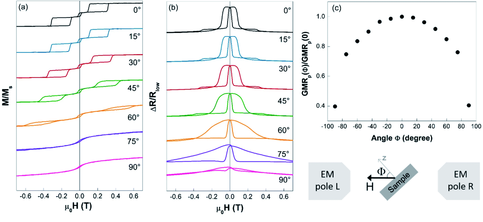 | ||
| Fig. 6 Room temperature (a) magnetic (M/Msvs. H) and (b) magneto-resistive (ΔR/Rlowvs. H) response of planar flexible GMR spin-valves (tCu = 3 nm) as a function of the angle Φ between the external applied field H and the film normal. All measurements were performed at room temperature. (c) Evolution of the GMR ratio normalized to the value at Φ = 0° as a function of the angle Φ, GMRP(Φ)/GMRP(0), as obtained from the curves in (b). The sketch illustrates the experimental configuration. | ||
Based on these results, the evolution of the GMR ratio as a function of the bending angle, GMRB(θ), is modeled as the integral of the experimental GMRP(Φ), where Φ accounts for the different angle that each portion of the sample forms with the magnetic field due to the bending. Referring to the sketch in the inset of Fig. 5c and d, the expected GMR ratio for the bended film under the magnetic field can be interpret as the result of the following integral:
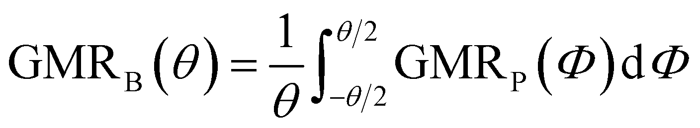 | (1) |
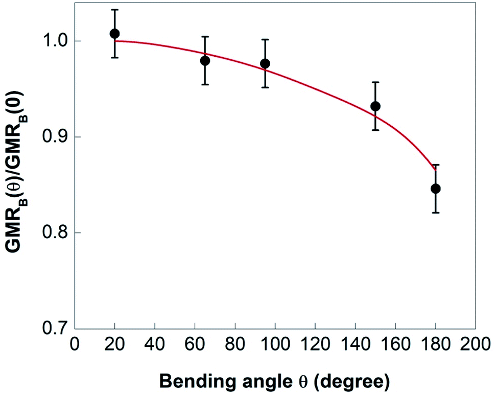 | ||
| Fig. 7 Experimental GMRB(θ) ratio (dots) normalized to the value measured on the flat sample (θ = 0°). Calculated values using eqn (1) are marked by a red line. | ||
Finally, it is worth mentioning that we do not detect a major effect of strain on the magneto-electric behaviour. Indeed, the GMR ratio of flat samples is the same as the one measured on the same samples at small bending angles (up to θ = 20°), where the magnetic field can be considered orthogonal to the surface within the experimental error bar. This suggests that the level of strain we applied, which meets the curvature of practical applications, does not imply any significant effect on the magneto-electric properties of our heterostructures.
4 Conclusions
In this work we demonstrated the feasibility of flexible magneto-resistive heterostructures with perpendicular magnetic anisotropy on large-area substrates through the use of a versatile Au-mediated transfer-and-bonding strategy. By exploiting the weak adhesion of an Au underlayer on SiOx/Si(100) substrates, perpendicular GMR-SVs with a GMR ratio of ∼1.5%, were efficiently transfered on commercial adhesive tapes by mechanical peel-off while preserving the whole magnetic and magneto-resistive properties despite the presence of very thin layers (down to 0.4 nm) forming the spinvalve thin film system. An improvement of the GMR ratio towards the limit of reference samples deposited on SiOx/Si (100) substrates is expected to be achieved by further reducing the Au surface roughness through a fine optimization of the deposition conditions. Magneto-resistance measurements versus bending revealed the magneto-electric robustness of these flexible structures, where the moderate change in the GMR ratio is mainly ascribed to the geometrical configuration with respect to the magnetic field rather than to a change of the electric behavior, thus paving the way for their integration on curved surfaces and the development of novel flexible devices requiring perpendicular magnetic anisotropy. The results also prove the effectiveness of the proposed Au-mediated transfer and bonding approach, which can be easily applied to other functional and flexible multilayer materials engineered at the nanoscale, including those whose fabrication process requires high temperature treatments that impedes the direct deposition on flexible polymeric tapes.Conflicts of interest
There are no conflicts to declare.Acknowledgements
C. R. acknowledges the PRIN project TWEET funded by the Italian Ministry of University and Research (MUR, project no. 2017YCTB59).References
- Flexible Electronics: Materials and Applications, ed. W. S. Wong and A. Salleo, Springer, 2009 Search PubMed.
- R. L. Crabb and F. C. Treble, Thin Silicon Solar Cells for Large Flexible Arrays, Nature, 1997, 213, 1223 CrossRef.
- M. Melzer and D. Makarov, A review on stretchable magnetic field sensorics, J. Phys. D Appl. Phys. Top., 2020, 53(1–34), 083002 CrossRef CAS.
- S. Huang, Y. Liu, Y. Zhao, Z. Ren and C. F. Guo, Flexible Electronics: Stretchable Electrodes and Their Future, Adv. Funct. Mater., 2019, 29(1–15), 1805924 CrossRef.
- D. Makarov, M. Melzer, D. Karnaushenko and O. G. Schmidt, Shapeable magnetoelectronics, Appl. Phys. Rev., 2016, 3, 011101 Search PubMed.
- F. An, et al., Highly Flexible and Twistable Freestanding Single Crystalline Magnetite Film with Robust Magnetism, Adv. Funct. Mater., 2020, 30(1–7), 2003495 CrossRef CAS.
- S. Han, et al., An Overview of the Development of Flexible Sensors, Adv. Mater., 2017, 29(1–22), 1700375 CrossRef.
- X. Wang, Z. Liu and T. Zhang, Flexible Sensing Electronics for Wearable/Attachable Health Monitoring, Small, 2017, 13(1–19), 1602790 CrossRef PubMed.
- Y. S. Rim, S. Bae, H. Chen, N. D. Marco and Y. Yang, Recent Progress in Materials and Devices toward Printable and Flexible Sensors, Adv. Mater., 2016, 28, 4415–4440 CrossRef CAS PubMed.
- Y. Liu, M. Pharr and G. A. Salvatore, Lab-on-Skin: A Review of Flexible and Stretchable Electronics for Wearable Health Monitoring, ACS Nano, 2017, 11, 9614–9635 CrossRef CAS PubMed.
- K. Fukuda, K. Yu and T. Someya, The Future of Flexible Organic Solar Cells, Adv. Energy Mater., 2020, 10(1–10), 2000765 CrossRef CAS.
- L. Li, Z. Wu, S. Yuan and X.-B. Zhang, Advances and challenges for flexible energy storage and conversion devices and systems, Energy Environ. Sci., 2014, 7, 2101–2122 RSC.
- S. Han, Y. Zhou and V. A. L. Roy, Towards the Development of Flexible Non-Volatile Memories, Adv. Mater., 2013, 25, 5425–5449 CrossRef CAS PubMed.
- S. Ota, A. Ando, T. Sekitani, T. Koyama and D. Chiba, Flexible CoFeB/MgO-based magnetic tunnel junctions annealed at high temperature (> 350 °C), Appl. Phys. Lett., 2019, 115(1–4), 202401 CrossRef.
- G. S. C. Bermúdez, H. Fuchs, L. Bischoff, J. Fassbender and D. Makarov, Electronic-skin compasses for geomagnetic field-driven artificial magnetoreception and interactive electronics, Nat. Electron., 2018, 1, 589–595 CrossRef.
- G. S. C. Bermúdez, et al., Magnetosensitive e-skins with directional perception for augmented reality, Sci. Adv., 2018, 4(1–9), 2623 CrossRef PubMed.
- S. Amara, et al., High-Performance Flexible Magnetic Tunnel Junctions for Smart Miniaturized Instruments, Adv. Eng. Mater., 2018, 20, 1800471–1800479 CrossRef.
- J. Chen, Y. Lau, J. M. D. Coey, M. Li and J. Wang, High Performance MgO-barrier Magnetic Tunnel Junctions for Flexible and Wearable Spintronic Applications, Sci. Rep., 2017, 7, 42001 CrossRef CAS PubMed.
- L. M. Loong, et al., Flexible MgO Barrier Magnetic Tunnel Junctions, Adv. Mater., 2016, 28, 4983–4990 CrossRef CAS PubMed.
- M. Melzer, et al., Imperceptible magnetoelectronics, Nat. Commun., 2015, 6(1–8), 6080 CrossRef CAS PubMed.
- A. Bedoya-Pinto, M. Donolato, M. Gobbi, L. E. Hueso and P. Vavassori, Flexible spintronic devices on Kapton, Appl. Phys. Lett., 2016, 104(1–5), 062412 Search PubMed.
- G. Lin, D. Makarov, M. Melzer, W. Si and O. G. Schmidt, A highly flexible and compact magnetoresistive analytic device, Lab Chip, 2014, 14, 4050–4058 RSC.
- M. Melzer, et al., Stretchable Magnetoelectronics, Nano Lett., 2011, 11, 2522–2526 CrossRef CAS PubMed.
- C. Barraud, et al., Magnetoresistance in magnetic tunnel junctions grown on flexible organic substrates, Appl. Phys. Lett., 2010, 96(1–4), 072502 CrossRef.
- B. Dieny, et al., Opportunities and challenges for spintronics in the microelectronics industry, Nat. Electron., 2020, 3, 446–459 CrossRef.
- V. K. Joshi, Spintronics: A contemporary review of emerging electronics devices, Eng. Sci. Technol. an Int. J., 2016, 19, 1503–1513 CrossRef.
- S. Bhatti, et al., Spintronics based random access memory: a review, Mater. Today, 2017, 20, 530–548 CrossRef.
- J. Ryu, S. Lee, K. Lee and B. Park, Current-Induced Spin – Orbit Torques for Spintronic Applications, Adv. Mater., 2020, 32(1–17), 1907148 CrossRef CAS PubMed.
- R. Bertacco and M. Cantoni, New trends in magnetic memories, in Ultra-high density magnetic recording-Storage Materials and Media Designs, ed. G. Varvaro and F. Casoli, Pan Stanford Publishing, 2016 Search PubMed.
- K. Yakushiji, A. Fukushima, H. Kubota, M. Konoto and S. Yuasa, Ultralow-voltage spin-transfer switching in perpendicularly magnetized magnetic tunnel junctions with synthetic antiferromagnetic reference layer, Appl. Phys. Express, 2013, 6(4pp), 113006 CrossRef.
- K. Yakushiji, H. Kubota, A. Fukushima and S. Yuasa, Perpendicular magnetic tunnel junctions with strong antiferromagnetic interlayer exchange coupling at first oscillation peak, Appl. Phys. Express, 2015, 8(4pp), 083003 CrossRef.
- M. Arora, et al., Magnetic properties of Co/Ni multilayer structures for use in STT-RAM, J. Phys. D Appl. Phys., 2017, 50(11pp), 505003 CrossRef.
- M. Arora, et al., Spin Torque Switching in Nanopillars With Antiferromagnetic Reference Layer, IEEE Magn. Lett., 2017, 8, 3100605 Search PubMed.
- Y. Chang, V. Garcia-vazquez, Y. Chang and T. Wu, Perpendicular magnetic tunnel junctions with synthetic antiferromagnetic pinned layers based on [ Co/Pd] multilayers, J. Appl. Phys., 2016, 113, 17B909 CrossRef.
- T. Devolder, et al., Annealing stability of magnetic tunnel junctions based on dual MgO free layers and [Co/Ni] based thin synthetic antiferromagnet fixed system, J. Appl. Phys., 2017, 121, 113904 CrossRef.
- Z. Li, Z. Zhang, H. Zhao, B. Ma and Q. Y. Jin, High giant magnetoresistance and thermal annealing effects in perpendicular magnetic [Co/Ni]N-based spin valves, J. Appl. Phys., 2015, 106, 013907 CrossRef.
- S. T. Lim, M. Tran, J. W. Chenchen, J. F. Ying and G. Han, Effect of different seed layers with varying Co and Pt thicknesses on the magnetic properties of Co/Pt multilayers, J. Appl. Phys., 2015, 117, 17A731 CrossRef.
- B. N. Engel, C. D. England, R. A. Van Leeuwen, M. H. Wiedmann and C. M. Falco, Interface Magnetic Anisotropy in Epitaxial Superlattices, Phys. Rev. Lett., 1991, 67, 1910–1913 CrossRef CAS PubMed.
- M. T. Johnson, P. J. H. Bloemen, F. J. A. Den Broeder and J. J. De Vries, Magnetic anisotropy in metallic multilayers, Rep. Prog. Phys., 1996, 59, 1409–1458 CrossRef CAS.
- S. Bandiera, et al., Comparison of Synthetic Antiferromagnets and Hard Ferromagnets as Reference Layer in Magnetic Tunnel Junctions With Perpendicular Magnetic Anisotropy, IEEE Magn. Lett., 2010, 1, 3000204 Search PubMed.
- J. A. Katine and E. E. Fullerton, Device implications of spin-transfer torques, J. Magn. Magn. Mater., 2008, 320, 1217–1226 CrossRef CAS.
- S. Yang, K. Ryu and S. Parkin, Domain-wall velocities of up to 750 ms−1 driven by exchange-coupling torque in synthetic antiferromagnets, Nat. Nanotechnol., 2015, 10, 221–226 CrossRef CAS PubMed.
- W. Legrand, et al., Room-temperature stabilization of antiferromagnetic skyrmions in synthetic antiferromagnets, Nat. Mater., 2020, 19, 34–42 CrossRef CAS PubMed.
- R. Chen, et al., Realization of Isolated and High-Density Skyrmions at Room Temperature in Uncompensated Synthetic Antiferromagnets, Nano Lett., 2020, 20, 3299–3305 CrossRef CAS PubMed.
- Z. Yu, et al., Voltage-controlled skyrmion-based nanodevices for neuromorphic computing using a synthetic antiferromagnet, Nanoscale Adv, 2020, 2, 1309–1317 RSC.
- M. Todeschini, A. Bastos, F. Jensen, J. B. Wagner and A. Han, Influence of Ti and Cr Adhesion Layers on Ultrathin Au Films, Appl. Mater. Interfaces, 2017, 9, 37374–37385 CrossRef CAS PubMed.
- L. Leandro, R. Malureanu, N. Rozlosnik and A. Lavrinenko, Ultrathin , Ultrasmooth Gold Layer on Dielectrics without the Use of Additional Metallic Adhesion Layers, Appl. Mater. Interfaces, 2015, 7, 5797–5802 CrossRef CAS PubMed.
- M. Donolato, C. Tollan, J. M. Porro, A. Berger and P. Vavassori, Flexible and Stretchable Polymers with Embedded Magnetic Nanostructures, Adv. Mater., 2013, 25, 623–629 CrossRef CAS PubMed.
- C. H. Lee, et al., Peel-and-Stick: Mechanism Study for Efficient Fabrication of Flexible/Transparent Thin-film Electronics, Sci. Rep., 2013, 3(1–6), 2917 CrossRef PubMed.
- C. H. Lee, D. R. Kim and X. Zheng, Fabrication of nanowire electronics on nonconventional substrates by water-assisted transfer printing method, Nano Lett., 2011, 11, 3435–3439 CrossRef CAS PubMed.
- G. F. Schneider, V. E. Calado, H. Zandbergen, L. M. K. Vandersypen and C. Dekker, Wedging transfer of nanostructures, Nano Lett., 2010, 10, 1912–1916 CrossRef CAS PubMed.
- F. J. A. Den Broeder, D. Kuiper, H. C. Donkersloot and W. Hoving, A comparison of the magnetic anisotropy of [001] and [111] oriented Co/Pd Multilayers, Appl. Phys. A, 1989, 49, 507–512 CrossRef.
- K. Tobari, M. Ohtake, K. Nagano and M. Futamoto, Preparation and characterization of Co/Pd epitaxial multilayer films with different orientations, Jpn. J. Appl. Phys., 2011, 50(1–7), 073001 CrossRef.
- G. Varvaro, et al., Co/Pd-Based synthetic antiferromagnetic thin films on Au/resist underlayers: Towards biomedical applications, Nanoscale, 2019, 11, 21891–21899 RSC.
- L. J. Van der Pauw, A Method of Measuring Specific Resistivity and Hall Effect of Discs of Arbitrary Shape, Philips Res. Reports, 1958, 13, 1–9 Search PubMed.
- S. K. Pandey and A. Manivannan, A fully automated temperature-dependent resistance measurement setup using van der Pauw method, Rev. Sci. Instrum., 2018, 89, 33906 CrossRef PubMed.
- J. E. Davies, et al., Reversal mode instability and magnetoresistance in perpendicular (Co/Pd)/Cu/(Co/Ni) pseudo-spin-valves, Appl. Phys. Lett., 2013, 103, 022409 CrossRef.
- N. Thiyagarajah and S. Bae, Effects of engineered Cu spacer on the interlayer coupling and giant magnetoresistance behavior in Pd/[Pd/Co]2/Cu/[Co/Pd]4 pseudo-spin-valves with perpendicular anisotropy, J. Appl. Phys., 2008, 104, 113906 CrossRef.
- N. ThiyagarajahI, L. LinI and S. BaeI, Effects of NiFe/Co Insertion at the [Pd/Co] and Cu Interface on the Magnetic and GMR Properties in Perpendicularly Magnetized [Pd/Co]/Cu/[Co/Pd] Pseudo Spin-Valves, IEEE Trans. Magn., 2010, 46, 968 Search PubMed.
- J. Qiu, et al., Effect of roughness on perpendicular magnetic anisotropy in (Co90Fe10/Pt)n superlattices, AIP Adv, 2016, 6(1–5), 056123 CrossRef.
- A. Paul, Effect of interface roughness on magnetic multilayers of Fe/Tb and Fe/Cr, J. Magn. Magn. Mater., 2017, 240, 497–500 CrossRef.
- M. Desai, A. Misra and W. D. Doyle, Effect of Interface Roughness on Exchange Coupling in Synthetic Antiferromagnetic Multilayers, IEEE Trans. Magn., 2005, 41, 3151–3153 CAS.
- E. Y. Tsymbal and D. G. Pettifor, Perspectives of Giant Magnetoresistance, in Solid State Physics vol 56, ed. H. Ehrenreich and F. Spaepen, Academic, New York, 2001, vol. 113–237 Search PubMed.
- S. Nakagawa and H. Yoshikawa, Effect of roughness and continuity of Co layers to magnetic properties of Co/Pd multilayers, J. Magn. Magn. Mater., 2005, 287, 193–198 CrossRef CAS.
- H. Oh and S. Joo, Enhancement of Coercivity by Underlayer Control in Co/Pd and Co/Pt Multilayers, IEEE Trans. Magn., 1996, 32, 4061–4063 CrossRef CAS.
Footnote |
| † Electronic supplementary information (ESI) available. See DOI: 10.1039/d1na00110h |
| This journal is © The Royal Society of Chemistry 2021 |