
 Open Access Article
 This Open Access Article is licensed under a Creative Commons Attribution-Non Commercial 3.0 Unported Licence
Morphology-dependent fluorescence of europium-doped cerium oxide nanomaterials†
Anne E.
D'Achille
a,
Robert M.
Wallace
 b and
Jeffery L.
Coffer
*a
b and
Jeffery L.
Coffer
*a
aDepartment of Chemistry and Biochemistry, Texas Christian University, Ft. Worth, TX. 76129, USA. E-mail: j.coffer@tcu.edu
bDepartment of Materials Science and Engineering, University of Texas at Dallas, Dallas, TX 75080, USA
First published on 28th April 2021
Abstract
Europium-doped CeO2 nanomaterials have been investigated for a variety of sensing and biological applications, as doping enhances the catalytic activity of CeO2 and contributes visible fluorescence to the nanomaterial. However, scant evidence is available that directly compares Eu3+ fluorescence from multiple morphologies establishing useful correlation(s) between physical and optical trends in such structures. To address this shortcoming, Eu3+-doped CeO2 nanorods, nanowires, nanocubes, and annealed nanorods were synthesized and characterized, representing a range of crystalline defect sizes, defect concentrations, and surface moieties. Morphologies rich with oxygen defects and hydroxyl groups (assessed via X-ray photoelectron spectroscopy) quenched the Eu3+ fluorescence, while samples with larger crystalline domains and lower Ce3+ concentrations have relatively stronger emission intensities. Of the four morphologies, nanocubes exhibit the strongest emission, as each structure is monocrystalline with few oxygen defects and associated quenching sites. Furthermore, the Eu3+ hypersensitive transition is more responsive to the dopant concentration in the nanocubes, as defects induced by the dopant are not removed by thermal annealing.
Introduction
Interest in cerium oxide (CeO2) nanomaterials continues to grow at a significant pace, due to ever-expanding applications in three-way catalytic converters,1 solid oxide fuel cells,2,3 radioprotective agents,4 oxygen5 and biological sensors,6 and enzyme mimetics,7,8 among others. This versatility stems from cerium's ability to easily convert between Ce3+ and Ce4+ oxidation states, as facilitated by the adsorption or release of oxygen. Methods to synthesize CeO2 nanomaterials have been extensively explored, with popular approaches including controlled precipitation,9,10 hydrothermal,11–13 sol–gel,14,15 surfactant-assisted,16 electrodeposition,17 and micellular methods. A range of morphologies including rods,11,12 cubes,18 wires,19 tubes,20 and polyhedral13 particles have been synthesized by adjusting the reaction parameters.Cerium is predominantly present as Ce4+ within the CeO2 structure, with a small concentration of Ce3+ defects charge balanced by oxygen vacancies.21 Manipulation of the ratio of Ce3+ to Ce4+ within a nanomaterial controls the nature of the CeO2 chemical activity as seen with the material's enzyme mimetic activity.8,22,23 Ce3+-rich materials act as superoxide dismutase mimetics, while Ce4+-rich samples mimic catalase.7,8,24 Reducing the nanoparticle dimensions25,26 and doping with lower-valent ions27,28 are two common approaches to increase the Ce3+/Ce4+ ratio, which is accompanied by an increase in oxygen vacancy concentration to maintain balanced charge within the nanomaterial.25–29
Other rare earth ions, which prefer the +3 oxidation state in many oxide phases, are easily doped into CeO2 nanomaterials due to similar ionic radii. The lower oxidation state of the dopant generates oxygen vacancies as well as Ce3+ defects to maintain charge balance.26,28 The resulting Ln3+-doped CeO2 (Ln–CeO2) nanomaterials have altered oxygen mobility, magnetism, catalytic reactivity, and fluorescence compared to the CeO2 host.30–32 In addition to controlling the Ce3+/Ce4+ ratio, doping CeO2 nanomaterials with known lanthanide fluorophores makes the structure fluorescent, eliminating the need for surface functionalization using fluorescent labels via post-fabrication processing.33–38
In terms of lanthanide ion choices, europium(III) is known for its intense red-orange emission and hypersensitive 5D0 → 7F2 transition. This transition is permitted only in the absence of an inversion symmetry, so the fluorescence associated with this hypersensitive transition in Eu3+ has been used in metal complexes and metal–organic frameworks as sensors/biosensors.39–43 The factors controlling fluorescence from the Eu–CeO2 nanoparticle morphology are the most thoroughly studied,44,45 with less thorough investigation of Eu–CeO2 films, rods, and nanowires or ribbons.33,34,38,46–48 Emission is believed to initiate with excitation of the O2− → Ce4+ charge transfer band, followed by energy transfer to Eu3+ and relaxation with emission of a photon. Ce3+ defects are proposed to aid the emission from Eu3+, but are typically accompanied by other intrinsic defects (oxygen vacancies, OH− groups, etc.) that facilitate non-radiative relaxation.33,49 Annealing removes these defects and associated non-radiative pathways, increasing overall emission intensity but weakens the hypersensitive transition in the 610–630 nm range as the removal of defects increases the symmetry about the Eu3+.46
At low dopant concentrations, emission intensity from Eu–CeO2 nanomaterials typically strengthens as the Eu3+ concentration is increased.34,47 Elevated dopant concentrations are associated with a stronger contribution from the hypersensitive transition, due to the introduction of defects.38,47,50 As the dopant concentration increases, the internal defects become more concentrated and the distance between Eu3+ ions is diminished, increasing the likelihood of self-quenching. Above a morphologically-dependent limit, quenching from these defects or other lanthanide ions prevents Eu3+ emission from the Eu–CeO2 nanomaterial.51,52
While considerable research is available regarding the photophysical properties of various Eu–CeO2 morphologies, many of these studies are focus only on one morphology or one dopant concentration, so a systematic comparison of emission as a function of morphology is lacking. In this paper, we report the synthesis and thorough characterization (scanning and transmission electron microscopies, energy dispersive X-ray spectroscopy, X-ray diffraction) of a well-defined series of morphologies through hydrothermal and electrospinning/annealing techniques. By comparing the optical properties of samples with similar dopant concentrations, we demonstrate the significant morphological dependence of emission intensity and asymmetry, associated with differences in surface chemistry, oxygen vacancy concentrations and Ce3+/Ce4+ ratios (as monitored indirectly by X-ray Photoelectron Spectroscopy (XPS)), and crystalline domain dimensions. Furthermore, the impact of Eu3+ concentration on the overall emission intensity, especially the hypersensitive transition, is found to be highly sensitive to CeO2 host morphology.
Methods and materials
All reagents purchased were of analytical grade. Polyvinyl-pyrrolidone (PVP, Mw ∼ 1![[thin space (1/6-em)]](https://www.rsc.org/images/entities/char_2009.gif) 300000), dimethyl-formamide (DMF), and methanol (MeOH) were purchased from Sigma Aldrich. MeOH and DMF were stored with molecular sieves. PVP was heated to 95 °C for 6 h, vacuum dried at room temperature overnight, and stored in a desiccator. All other chemicals were used as received with no further purification. Acetone and ethanol (95%) were purchased from Pharmco-Aaper. Cerium(III) chloride heptahydrate (CeCl3·7H2O), europium(III) nitrate hexahydrate (Eu(NO3)3·6H2O), and sodium hydroxide (NaOH) were purchased from Alfa Aesar. Europium(III) chloride hexahydrate (EuCl3·6H2O) was purchased from Strem. Cerium(III) nitrate heptahydrate (Ce(NO3)3·7H2O) was purchased from Acros Organics. Tribasic sodium phosphate dodecahydrate (Na3PO4·12H2O) was purchased from Mallinckrodt.
300000), dimethyl-formamide (DMF), and methanol (MeOH) were purchased from Sigma Aldrich. MeOH and DMF were stored with molecular sieves. PVP was heated to 95 °C for 6 h, vacuum dried at room temperature overnight, and stored in a desiccator. All other chemicals were used as received with no further purification. Acetone and ethanol (95%) were purchased from Pharmco-Aaper. Cerium(III) chloride heptahydrate (CeCl3·7H2O), europium(III) nitrate hexahydrate (Eu(NO3)3·6H2O), and sodium hydroxide (NaOH) were purchased from Alfa Aesar. Europium(III) chloride hexahydrate (EuCl3·6H2O) was purchased from Strem. Cerium(III) nitrate heptahydrate (Ce(NO3)3·7H2O) was purchased from Acros Organics. Tribasic sodium phosphate dodecahydrate (Na3PO4·12H2O) was purchased from Mallinckrodt.
Synthesis of Eu–CeO2 nanowires
The Eu–CeO2 nanowires were synthesized by a sol–gel reaction, followed by electrospinning to produce metal–polymer composite nanowires. The polymer template was subsequently removed through a two-step annealing process to produce the desired nanowire product. In a typical reaction, 0.25 g PVP was dissolved in 1.5 g dry MeOH while 0.3 g (0.70 mmol) Ce(NO3)3 and 0.0–0.06 g (0–0.13 mol) Eu(NO3)3 were dissolved in 1.0 g dry DMF. Once dissolved, the two solutions were rapidly stirred for 20 s until any visible precipitates dispersed, then gently shaken for 10 min to release any air bubbles. The solution was transferred to a syringe, which was connected to a long cannula terminated with a 25 mm,16-gauge metal needle. The polymer solution was injected (via a syringe pump) at a speed of 0.8 mL h−1 into an electric field with a voltage of 20 kV for a minimum of 15 min. A rotating drum covered with Al foil was placed 12 cm from the syringe tip and used as the counter electrode (Fig. S1†). To anneal, the metal–polymer nanowire films were removed from the collecting drum and sandwiched between two Si plates. The films were first gradually heated in ambient air (1 atm) to 220 °C over the course of 3 h (∼1 °C min−1) in an oven, held at that temperature for 16 h, then gradually cooled to room temperature over a 5 hour period. Once cooled, the Si plates containing the nanowire films were heated (air, 1 atm) to 950 °C over the course of 5 h (∼3 °C min−1) in a tube furnace, maintained at that temperature for 16 h, then cooled to room temperature over 6 h to yield white flakes weighing 5–20 mg.Synthesis of Eu–CeO2 nanorods
CeO2 and Eu–CeO2 nanorods were synthesized by modification of well-established hydrothermal procedures.53,54 In a typical reaction, 0.3 g (0.81 mmol) CeCl3 and 0.0–0.04 g (0–0.12 mmol) EuCl3 were dissolved in 4.5 mL H2O, and 0.018 g (0.05 mmol) Na3PO4 dissolved in 13.9 mL of 2.5 M NaOH. The final reactant concentrations were 44 mM CeCl3, 0–6.5 mM EuCl3, and 2.7 mM Na3PO4. The solutions were mixed and rapidly stirred in an ice bath at 0 °C for 20 min, transferred to a 50 mL Teflon screw-cap reactor, and heated at 100 °C in an oven for 16 h. The samples were washed while hot with three cycles of ethanol and water, dry at 100 °C, and ground to yield ∼100 mg of a light yellow powder.Synthesis of Eu–CeO2 annealed nanorods
Annealed nanorods were produced from the Eu–CeO2 nanorods as described above. The dry and ground nanorod powder was transferred to a quartz boat and placed in an oven. The annealed rods were heated to 500–800 °C (ambient air, 1 atm) over the course of an hour (∼8–14 °C min−1), maintained at that temperature for 16 h, then allowed to cool gradually to room temperature to yield a white/pale yellow powder.Synthesis of Eu–CeO2 nanocubes
CeO2 and Eu–CeO2 nanocubes were synthesized by a previously-reported hydrothermal procedure.53,54 Briefly, 0.4 g (0.92 mmol) Ce(NO3)3 and 0.0–0.054 g Eu(NO3)3 (0–0.12 mmol) were dissolved in 6.6 mL H2O. 13.3 mL of 15 M NaOH was added to yield final concentrations of 46 mM Ce3+, 0.0–6.0 mM Eu3+, and 10 M OH−. The reaction mixture was rapidly stirred in an iced acetone bath at 0 °C for 20 min, transferred to a 20 mL stainless steel-coated Teflon vessel, and placed in an oven preheated to 180 °C for 16 h. After allowing the reactor to cool naturally, samples were washed with water, dry and ground into ∼150 mg of white powder.Characterization
The morphology of the Eu–CeO2 nanorods was characterized by Transmission Electron Microscopy (TEM) and High Resolution TEM (HRTEM) using a JEOL 2100 TEM operating at 200 kV. Samples were first sonicated in de-ionized water for 2 min, then a drop of the suspension was transferred to a carbon coated copper grid and allowed to evaporate prior to analysis. Elemental data was collected using EDAX Energy Dispersive Spectroscopy Unit (EDS) attached to the JEOL 2100.Powder X-ray diffraction (XRD) data was acquired using a Philips XRG3100 using Cu Kα radiation, with step size of 0.02 deg and step time of 20 seconds in the 10–80° 2Θ range. Sample peak positions were compared to CeO2 reference sample data from the National Institute of Standards and Technology (NIST), Standard Reference Material 674b.55
X-ray Photoelectron Spectroscopy (XPS) measurements were made on a PerkinElmer Phi 560 XPS/Auger system using a non-monochromatic Mg/Al X-ray source (nanorods, nanocubes, annealed nanorods) and a PHI 5000 Versa Probe II equipped with a monochromatic Al Kα and a hemispherical analyzer (nanowires). All nanowire XPS data were taken with a pass energy of 23.5 eV, while XPS data for the other samples were taken with a pass energy of 100 eV for survey scans and 50 eV for detailed scans. The energy scale calibration for XPS is done using clean metal foils (polycrystalline Cu, Ag, Au) across the (binding) energy scale according to ASTM E2108-16. The scans were charge corrected (by a magnitude of no more than 1 eV) to adventitious carbon and assumed with have a binding energy of 284.6 eV. The Ce 3d and O 1s regions were fitted using CasaXPS software using Shirley backgrounds.
Spectroscopic analysis
For selected fluorescence measurements, the above Eu–CeO2 nanomaterials were excited at a wavelength of 370 nm using a mercury lamp equipped with a ±5 nm bandpass filter. Fluorescence images were taken on a Nikon fluorescence microscope and associated fluorescence spectra were recorded using an Ocean Optics 1000 series spectrometer interfaced to the above microscope. Fluorescence was acquired with a 100 ms integration time, unless otherwise noted.Fluorescence and UV-Vis absorbance spectra were also recorded for these nanomaterials as aqueous suspensions. Three mg of 8 at% Eu–CeO2 nanocubes were suspended in 5 mL of DI H2O to make a stock solution. The stock solution was diluted until the peak absorbance was between 1.3 and 1.4. The diluted solutions were 112 μg mL−1 for nanocubes, 260 μg mL−1 for nanorods, 188 μg mL−1 for annealed nanorods, and 75 μg mL−1 for nanowires. These concentrations were used to obtain fluorescence and UV-Vis absorbance spectra of all suspended nanomaterials.
UV-Vis spectra were collected using an Agilent Cary 60 UV-Vis spectrometer in the 200–800 nm range. Selected fluorescence spectra were collected on a Shimadzu RF-5301 PC spectrofluorometer, with excitation at 375 nm, measuring emission from 400 nm to 700 nm, and using slit widths of 5 mm.
Results – nanomaterial characterization
Morphology
The morphologies of the four nanomaterials (nanowires, nanorods, nanocubes, annealed nanorods) were first characterized using transmission electron microscopy (TEM). The target Eu3+ concentration with regard to atomic percentage within each material ranges from 0% to 18% Eu3+, as calculated by eqn (S1)† and based on experimental reactant concentrations.Shown in Fig. 1 are the TEM images of the 8% Eu–CeO2 of the above morphologies, where 8% indicates the target Eu concentration. This Eu3+ concentration is selected on the basis of its near-optimal emission intensity and associated absence of clustering/phase segregation of the lanthanide species in a given CeO2 matrix. The nanowires are synthesized in and retain an interconnected network, due to the nature of the electrospinning process (Fig. 1a). The metal salts were dispersed into a polymer solution which was then injected into a strong electric field. Thin jets of this solution are ejected due to surface charge repulsion (Fig. S1†), whipping in transit to a collection drum, and depositing as long metal ion-loaded polymer nanowires (Fig. S2†). Annealing removes the template without loss of the network morphology. The nanowire lengths are difficult to measure due to their non-linear morphology and a lack of discrete boundaries but are estimated to be ∼1–2 μm. The nanowire diameter can be manipulated between 80 nm and 300 nm by adjusting the solvent ratio, but for this work the nanowire diameters are kept near 100 nm (Table 1 and Fig. S3†). Doping the nanowires with Eu3+ is accomplished by addition of Eu(NO3)3 to the electrospinning solution, and had no detectable influence on the resultant nanowire morphology.
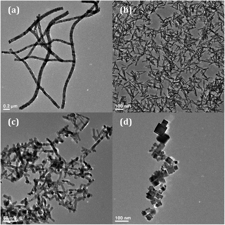 | ||
| Fig. 1 TEM images of 8% Eu–CeO2 (a) nanowires; (b) nanorods; (c) annealed nanorods; and (d) nanocubes. | ||
| Sample | Width (nm) | Length (nm) |
|---|---|---|
| Nanowires | 108 ± 25 | >1 μm |
| Nanorods | 11 ± 3 | 91 ± 21 |
| Annealed nanorods | 19 ± 6 | 59 ± 29 |
| Nanocubes | 25 ± 11 | — |
In contrast to the nanowire template-based approach, the hydrothermal synthesis of nanocubes and nanorods uses the relative growth and oxidation of Ce(OH)3 and CeO2 to control CeO2 morphology. Ce(OH)3 precipitates upon mixing of the Ce3+ and OH− solutions. By heating under pressure, Ce(OH)3 nanorods grow through Oswald ripening, which are converted to CeO2 during the washing and drying steps. While occasional dense aggregates are observed, typically the nanorods grow with an average length of 91 nm and an average width of 11 nm (Fig. 1b and Table 1). The nanorods were annealed in air at 800 °C to remove defects and reduce the hydroxide presence. After annealing in air, some sintering was observed with increased fusion between rods (Fig. 1c). The nanorod length was reduced from 91 nm to 59 nm, and width increased from 11 nm to 19 nm (Table 1 and Fig. S3†).
By using higher concentrations of OH–, eliminating Na3PO4, and carrying out the hydrothermal reaction at 180 °C, nanocubes are synthesized instead of nanorods. The Ce(OH)3 nuclei dissolve given the higher pressure and temperature, and the Ce3+ is oxidized to Ce4+ prior to precipitation as small CeO2 nuclei. The nanocubes grow through oriented attachment, with average edge lengths of about 25 nm (Fig. 1d, Table 1 and Fig. S3(f)†). Due to attraction between individual cubes, they appear as small clusters under 200 nm in diameter.
Crystallinity
The 8% Eu nanowires, nanocubes, nanorods, and annealed nanorods were characterized through powder X-ray diffraction (XRD) to determine their crystal structure, detect any possible phase separation of europium oxide (Eu2O3) or Ce2O3, and estimate crystalline domain size. CeO2 crystallizes in a cubic fluorite structure, with cerium ions arranged in a face centered cubic lattice and oxygen ions in the tetrahedral holes. The XRD patterns of 8% Eu–CeO2 nanorods, nanocubes, nanowires, and annealed nanorods are shown in Fig. S4,† indicating that all four morphologies are composed of CeO2 in the cubic fluorite phase.12 No evidence of Eu2O3 or other crystal phases is observed in any sample. Relative crystalline domain sizes were determined by a Scherrer analysis of broadening from the (111) reflection (ESI†). The calculated domain sizes are consistent with the peak broadening seen in Fig. S4,† with the nanorods and nanocubes assigned the smallest and largest domains, respectively (Table 2). Annealing the nanorods increases the domain size from 6 nm to 16 nm, consistent with sintering and fusion of the nanorods.| Sample | FWHM (2Θ) | XRD crystalline domain (nm) |
|---|---|---|
| Nanowires | 0.5 | 17 |
| Nanocubes | 0.38 | 22 |
| Nanorods | 1.44 | 6 |
| Annealed nanorods | 0.58 | 16 |
Each morphology was also characterized using HRTEM to further investigate differences in crystallinity and exposed lattice faces. All lattice spacings observed in each sample morphology are assignable to the (111), (200), and (220) planes of the cubic fluorite CeO2 crystal structure.12 However, the samples differed regarding which of the three CeO2 planes were exposed, the size of the crystalline domains, and whether the nanomaterial was monocrystalline or polycrystalline.
At high magnification, the 8% Eu–CeO2 nanowires are composed of fused nanoparticles about 15–20 nm in diameter (Fig. 2a). The lattice spacing is difficult to image, due to reduced electron transmission through the thick nanowires. Despite this, some fringes can be observed in small protruding nanoparticles. Each of these nanoparticles is monocrystalline, typically with the CeO2 cubic fluorite (111) plane exposed. Occasionally one crystalline domain expands past one nanoparticle into the neighboring fused particles. The 8% Eu–CeO2 nanocubes are also monocrystalline, with clusters of nanocubes commonly consisting of one domain due to their growth through oriented attachment (Fig. 2d). Consistent with previously published literature, the nanocubes expose higher energy (200) lattice planes, with the (111) and (220) lattice fringes occasionally observed.56
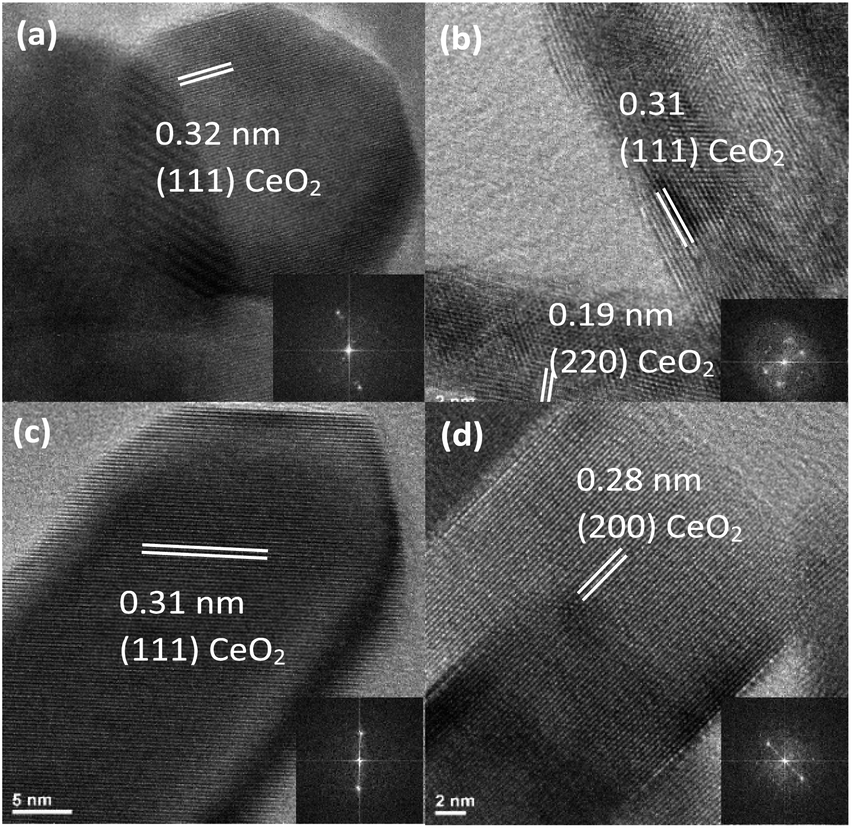 | ||
| Fig. 2 HR-TEM images with lattice spacings of 8% Eu–CeO2 (a) nanowires, (b) nanorods, (c) annealed nanorods, and (d) nanocubes. Inset in each HRTEM image is the respective fast fourier transform (FFT). | ||
In contrast, the nanorods are polycrystalline, with each rod exposing several crystalline planes within one rod (Fig. 2b). The highest energy plane, (220), often runs perpendicular to the length of the rod or needle, while (111) planes run both diagonally and parallel to the nanorod length. Two to five nanometer domains are also often observed, with random orientation relative to the remainder of the particle. The conversion from Ce(OH)3 to CeO2 during washing and drying results in rapid crystallization at several locations within a single particle, consistent with the observed polycrystallinity. Upon annealing the nanorods, the individual crystalline domains are sintered into one large domain that encompasses the entire nanorod (Fig. 2c). The (220) plane is no longer observed, with only the (111) lattice fringes observed, similar to the nanowires.
Elemental characterization
All four morphologies were characterized using energy dispersive X-ray spectroscopy (EDS) to determine elemental composition. The EDS spectra showed the expected elements, namely cerium, oxygen, and europium (Fig. 3a). Copper and carbon peaks were also observed due to the carbon-coated copper mesh sample holder and a Si artefact was occasionally observed, with no other contaminants. Oxygen, europium, and cerium were relatively evenly distributed throughout the nanowires, as seen by elemental mapping of the 8% Eu–CeO2 nanowires (Fig. 3b–e). The atomic concentrations were calculated assuming cerium, europium, and oxygen to be the only significant components (Tables 3, S1 and S2†).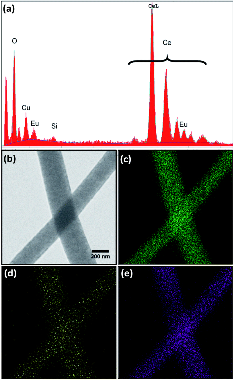 | ||
| Fig. 3 (a) Representative EDS spectrum of 8% Eu–CeO2 nanowires, with corresponding (b) STEM image, and elemental maps of (c) cerium (d) europium, and (e) oxygen, elemental maps. | ||
| Sample | Metal and oxygen concentrations | Metal elements only | |||
|---|---|---|---|---|---|
| At% O | At% Ce | At% Eu | At% Ce | At% Eu | |
| Nanowire | 53.1 ± 4.3 | 42.3 ± 3.8 | 4.6 ± 0.9 | 90.3 ± 1.7 | 9.7 ± 1.7 |
| Nanorod | 62.1 ± 5.5 | 34.2 ± 4.6 | 3.7 ± 0.9 | 92.1 ± 1.7 | 7.9 ± 1.7 |
| Annealed nanorod | 60.2 ± 1.9 | 36.9 ± 2.1 | 2.8 ± 0.4 | 93.0 ± 0.9 | 7.0 ± 0.9 |
| Nanocube | 54.3 ± 3.6 | 42.6 ± 3.7 | 3.1 ± 0.2 | 93.2 ± 0.9 | 6.8 ± 0.9 |
The use of EDS to quantify oxygen concentrations is somewhat unreliable as oxygen is a relatively mobile species in a focused electron beam. The nanorod and annealed nanorod morphologies show slightly elevated oxygen concentrations relative to the nanocube and nanowire samples. Since the nanorods are initially synthesized as Ce(OH)3 with rapid oxidation to CeO2, trace amounts of Ce(OH)3 may remain in the nanorod, increasing the oxygen-to-cerium ratio. The oxygen concentration is somewhat lower in the nanowires and nanocubes compared to the rod samples. The nanocube synthesis is driven by oriented attachment of CeO2 nanoparticles, reducing the likelihood of trapped hydroxide species, while the nanowires have a slightly higher concentration of Eu3+, increasing the oxygen defect concentration.
XPS analysis
To more quantitatively determine the influence of morphology on the Ce3+/Ce4+ ratio and oxygen defect concentration, XPS measurements were performed on the four 8% Eu–CeO2 nanomaterials (nanorods, nanocubes, nanowires, annealed nanorods), as well as undoped CeO2 nanorods. After fitting of the Eu–CeO2 nanorod's core level Ce 3d spectral region, six peaks at 881.8, 888.2, 898.0, 900.6, 906.7, and 916.4 eV were assigned to Ce4+, while two peaks at 884.7 and 903.2 eV were assigned to Ce3+ (Fig. 4a and Table S4†). Similar components were identified in the Ce 3d spectrum of the Eu–CeO2 annealed rods, with negligible shifts in binding energy of 0.3 eV or less (Fig. 4b and Table S4†). Similar peak fitting was used for the Eu–CeO2 nanowires and Eu–CeO2 nanocubes (Tables S3, S4 and Fig. S5†).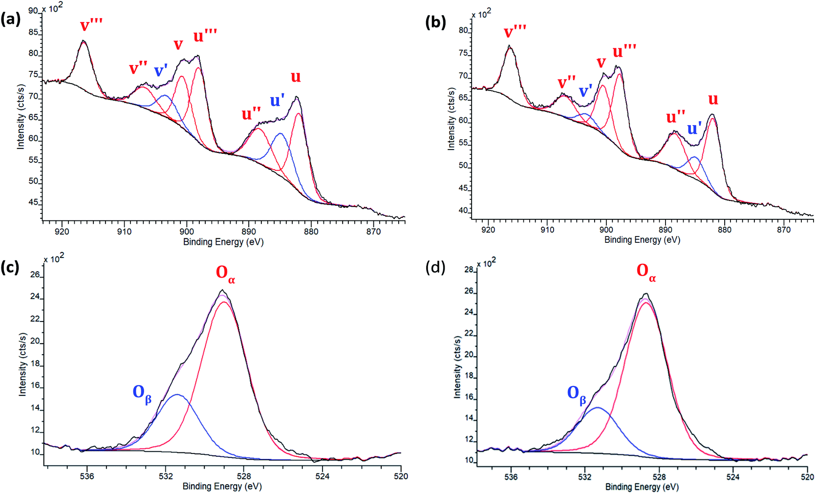 | ||
| Fig. 4 XPS spectra of 8% Eu–CeO2 (a) Ce 3d region of nanorods; (b) Ce 3d annealed nanorods; and (c) O 1s region of nanorods, and (d) O 1s of annealed nanorods. | ||
The concentration of Ce3+ ions within the nanomaterial can then be calculated using the integrated areas of the fitted peaks, as written in eqn (1) where Ax is the area of the peak “x”.
 | (1) |
Since the nanorods are synthesized as Ce(OH)3 prior to drying with no high temperature annealing treatment, the Ce3+ concentration was highest in the nanorod morphology (20.1%), followed by the nanocubes (15.1%), annealed nanorods (10.4%), and finally the nanowires (8.2%).
The O 1s spectrum for the above CeO2 nanomaterials (Fig. 4c and d) was fitted to show two peaks, Oα and Oβ. Oα is typically associated with lattice oxygen and Oβ accounts for surface oxygen as well as oxygen near crystal defects. The undoped CeO2 nanorods had a Oβ percentage of 17.4%, which increased upon doping to 25.7% due to the internal defects induced by the presence of Eu3+. Annealing the nanorods reduces the percentage of Oβ down to 20.2%, as defects and/or surface hydroxides are eliminated. The nanocubes and nanowires had the lowest Oβ concentrations of 9.7% and 13.6% respectively.
Results – optical properties
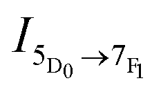
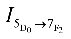
Europium(III) is well known for its hypersensitive electric dipole (ED) transition, 5D0 → 7F2, which is parity forbidden, and thus is particularly sensitive to surrounding inversion symmetry. The emission is forbidden if the ion is located in more symmetrical environments, and therefore Eu3+ has been used as to probe local structure.57 In addition to this ED hypersensitive 5D0 → 7F2 transition emitting in the 610–630 nm region, europium has another transition of particular interest, the magnetic dipole (MD) 5D0 → 7F1 transition emitting near 590 nm which is relatively insensitive to the local environment.58Analysis of asymmetry about the Eu3+ ion is well-established, typically quantified by the asymmetry ratio, R21, which compares the integrated area of the two transitions as defined in eqn (2).58 Higher R21 values correspond with insertion of the Eu3+ ion into relatively more asymmetric environments, due to the increased emission intensity of the hypersensitive transition.
 | (2) |
Fluorescence from europium-doped cerium oxide has been previously reported in several CeO2 morphologies, including particles,33 wires,51 and rods.50 The Eu3+ ions substitute into the highly symmetrical Ce4+ site, suppressing emission through the 5D0 → 7F2 transition, and lowering the R21 ratio.47,59 Introduction of defects, such as oxygen vacancies and accompanying Ce3+ ions also disrupts the CeO2 lattice, breaking the inversion symmetry and increasing the asymmetry ratio.60 However, these defects may also facilitate non-radiative relaxation, thereby suppressing Eu3+ emission intensity.
Fluorescence: excitation at 370 nm
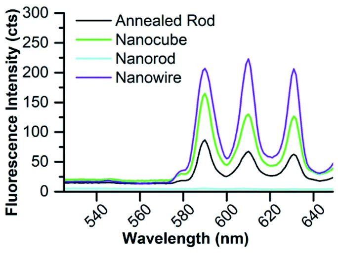
The nanomaterials were first investigated as dry powders or films using a 370 nm excitation wavelength to minimize scattering (as seen in the UV-Vis absorption spectra). Upon excitation at 370 nm, the 8% Eu–CeO2 nanocubes, nanowires, and annealed nanorods all exhibit strong red fluorescence (Fig. 5a, c, d and 6), associated with previously reported Eu3+ luminescence spectra of Eu–CeO2 materials.33,50,51 In contrast, no visibly detectable emission was observed from the as prepared nanorods (Fig. 5b).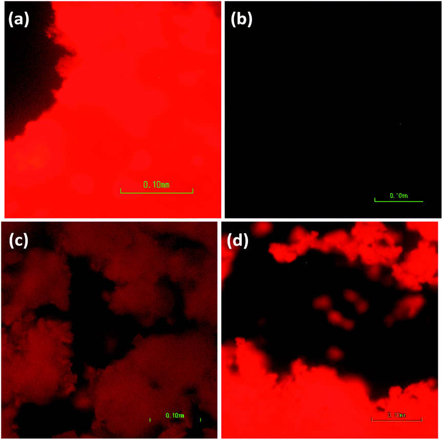 | ||
| Fig. 5 Images of emission from 8 at% Eu–CeO2 (a) nanowires, (b) nanorods, (c) annealed nanorods, and (d) nanocubes, following excitation at 375 nm, with acquisition time of 800 ms. | ||
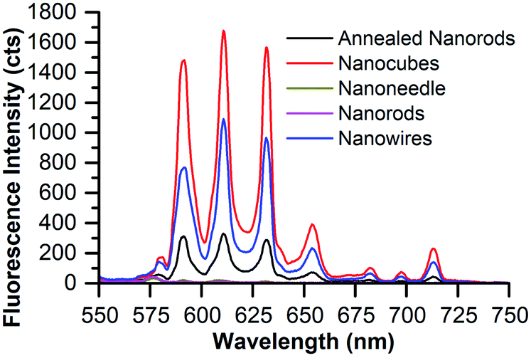 | ||
| Fig. 6 Emission of 8% Eu–CeO2 dry powder or film samples following excitation at 375 nm with 100 ms acquisition time. | ||
Eu–CeO2 systems are prone to Eu3+ fluorescence quenching through non-radiative relaxation facilitated by surface hydroxyls or oxygen vacancies within the material;28,33 so the 8% Eu–CeO2 nanorods were annealed to increase Eu3+ emission intensity by ideally removing defects. Weak emission is first detected after annealing to 400 °C and intensifies with increasing annealing temperature (Fig. 7). The asymmetry ratio decreases with increasing annealing temperature, driven in part by the sharpening of the hypersensitive peak at 610 nm due to reduction of a shoulder near 606 nm. The presence of this shoulder at low annealing temperatures suggests that the symmetry around the europium ions may be broken by several different types of defects (Ce3+, oxygen vacancy, hydroxyl group, etc.).61 The removal of some of these defects, leaving only Ce3+ and oxygen vacancies as required by europium-induced charge balance, is reflected in the peak sharpening and disappearance of the shoulder if the nanorods are annealed to 700 °C or higher.
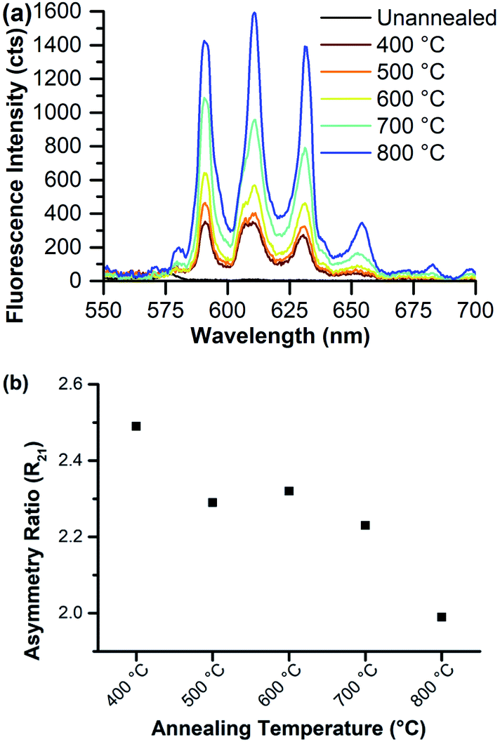 | ||
| Fig. 7 8% Eu–CeO2 nanorods annealed to various temperatures and excited at 375 nm, showing (a) fluorescence spectra; and (b) asymmetry ratio values as a function of annealing temperature. | ||
It should be pointed out, however, that the strongly fluorescing nanocubes are also synthesized through a hydrothermal reaction and should also be covered with the same functional moieties. The difference in emission of the nanorods and nanocubes may be explained in part by the rapid oxidation of the nanorods and their smaller crystal domains. These domains in principle allow more defects, which may act as sites of emission quenching. Hydroxide species not removed from the nanorods due to rapid oxidation also act to quench the Eu3+ emission.
Therefore, we propose two separate stages of fluorescence activation. Quenching species such as surface hydroxyls are eliminated at temperatures below 600 °C (Fig. S6†) so the nanorods exhibit weak Eu3+ emission. Removal of internal and/or surface defects such as oxygen vacancies and Ce3+ defects occurs at higher temperatures. The removal of these defects reduces the asymmetry about the Eu3+ centers, as reflected in the reduction of the asymmetry ratio with a concurrent enhancement of fluorescence intensity.
Fluorescence: excitation at 340 nm
The emission from suspended Eu–CeO2 nanomaterials was then measured following excitation at 340 nm, the absorbance maximum (Fig. S7 and S8†). Comparisons of emission intensity between morphologies is not feasible, as each morphology is suspended using a different concentration limited by size-dependent scattering. However, the Eu3+ asymmetry ratios may still be calculated and compared as they are an intrinsic property and independent of concentration. Furthermore, the influence of Eu3+ concentration may be compared between samples of similar morphology, due to the negligible influence of Eu3+ on morphology and size.As previously described, the nanocubes have the most intense emission of the four morphologies when excited as a dry powder at 375 nm. For this reason, the excitation spectrum was collected for the nanocubes, monitoring emission at 590 nm (Fig. S9†). As anticipated, the maximum emission is observed with excitation near 340 nm, consistent with CT excitation of host CeO2 and energy transfer to Eu3+. Insignificant peaks are also observed at 500 nm and 620 nm, representing weak direct excitation of Eu3+ through the 7F0 → 5D0 and 7F2 → 5D0.
Representative fluorescence spectra of the suspended 8% Eu–CeO2 samples, following excitation at 340 nm using a commercial fluorimeter are shown in Fig. 8. The asymmetry ratios (R21) calculated from these spectra are listed in Table 4. The asymmetry ratio loosely tracks with the crystalline domain size, with the nanocubes showing the lowest asymmetry followed by the annealed nanorods and finally the nanowires. As CeO2 nanoparticles with small crystalline domains typically exhibit higher defect concentrations,62 Eu3+ ions doped into materials with small domains are more likely to be in an asymmetrical site. However, compared to the variation in asymmetry ratio observed with changing Eu3+ concentration, the differences between morphologies are relatively small.
 | ||
| Fig. 8 Emission of 8 at% Eu–CeO2 nanowires (75 μg mL−1), nanorods (260 μg mL−1), nanocubes (112 μg mL−1), nanorods (260 μg mL−1) and annealed nanorods (188 μg mL−1) following excitation at 340 nm with 100 ms acquisition. | ||
| Sample |
|
|
Asymmetry ratio (R21) |
|---|---|---|---|
| Nanowire | 2087 | 4030 | 1.93 |
| Nanorod | 145 | 72 | 1.99 |
| Annealed nanorod | 1420 | 782 | 1.81 |
| Nanocube | 2636 | 1512 | 1.74 |
Each morphology was synthesized at target Eu3+ concentrations of 0–15%, then analyzed for differences in Eu3+ emission intensity and asymmetry ratio (Table 4 and Fig. 9). Emission from the nanorods was extremely weak, regardless of europium concentration or emission acquisition parameters. In addition, no emission is observed for any undoped morphology except the nanowires with an extremely weak 7F0 → 5D1 emission at 590 nm, attributed to a small Eu3+ contamination. Therefore, the following analysis is limited to the doped nanowires, nanocubes, and annealed nanorods.
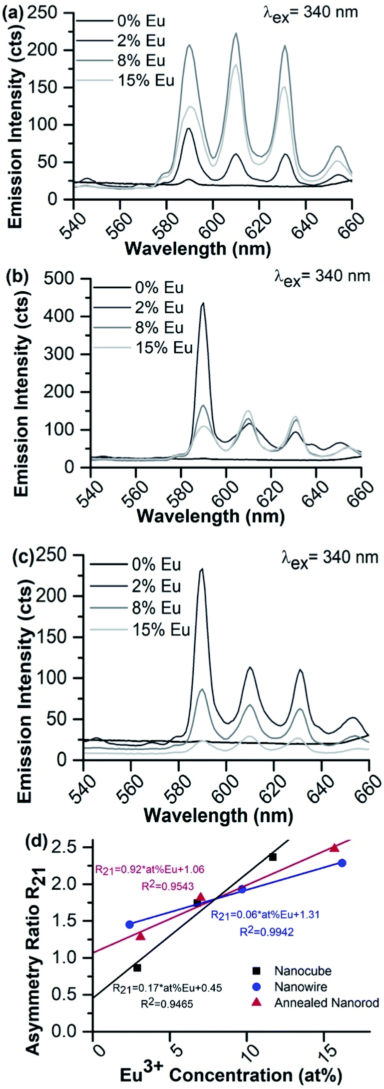 | ||
| Fig. 9 Fluorescence of target 0–15% Eu3+-doped CeO2 (a) nanowires; (b) nanocubes; (c) annealed nanorods; and (d) the calculated asymmetry ratio for various Eu3+ concentrations, all following excitation at 340 nm. | ||
If CeO2 is doped with relatively low concentrations of europium, the europium substitutes into the highly symmetrical Ce4+ sites of the CeO2 crystal lattice with minimal nearby asymmetry, so emission from the hypersensitive 7F0 → 5D2 transition at 610 nm and 630 nm is suppressed.34 Increasing the Eu3+ concentration generates more Ce3+ defects and oxygen vacancies, breaking the inversion symmetry about the emitting ion and allowing the hypersensitive transition. However, most Eu3+-containing nanomaterials suffer from concentration quenching, limiting emission intensity overall at higher doping concentrations.
The fluorescence spectra of the 2% Eu–CeO2 nanomaterials are all dominated by intense emission from the 7F0 → 5D1 MD transition at 590 nm, while emission through the 7F0 → 5D2 hypersensitive peaks at 610 and 630 nm is relatively suppressed (Fig. 9). Increasing the Eu3+ concentration to 8% quenches the MD transition by about 60% for the nanocubes and annealed nanorods, while the intensity doubles for the nanowires. This emission is further quenched in the most heavily-doped nanocubes and annealed nanorods, with an overall decrease in fluorescence of 60% and 85%, respectively. The MD transition is also less intense in the 15% Eu3+ nanowire samples compared to the 8% sample, but is still relatively 60% stronger than the 2% doped sample.
Manipulation of the Eu3+ concentration has a unique impact on the hypersensitive emission intensity from each of the three morphologies. In the nanocubes, the fluorescence intensity increases by less than 10%, consistent with the introduction of new defects into the crystal lattice. In contrast, the hypersensitive transition emission steadily weakens with increasing Eu3+ concentrations in the annealed nanorods, suggesting an increased likelihood of lanthanide self-quenching. In the nanowires, the hypersensitive transition mirrors the behavior of the MD transition, more than doubling in intensity when the Eu3+ concentration is increased from 2 at% to 8 at%, then slightly weakening at 8 at% to 15 at% respectively. The calculated asymmetry ratio reflects these trends between materials (Fig. 9d). The R21 ratio is more sensitive to the Eu3+ concentration in the nanocube morphology compared to the nanowires or annealed nanorods, due to the significant quenching at 590 nm in the nanocube sample coupled with slight intensification of the hypersensitive transition. R21 also increases for the nanowires and annealed nanorods, but in a manner far less sensitive to [Eu3+] compared to the nanocubes. Annealing the CeO2, as required during synthesis of the nanowires and annealed nanorods (Table S5†), minimizes the presence of defects such as oxygen vacancies or Ce3+ ions, reducing the asymmetry observed by the emitting Eu3+.
Conclusions
A series of doped CeO2 nanomaterials have been synthesized with morphological control, and subsequently doped with europium in an effort to understand the relationship between morphology and fluorescent properties. The four morphologies present a range of dimensions, Ce3+/Ce4+ ratios, surface chemistries, and crystalline defects with an important impact on the Eu3+ emission. The CeO2 nanowires and nanocubes were successful hosts for Eu3+ doping, both intensely emitting when excited at 340 nm due to large crystalline domains and minimal defects which would otherwise quench the fluorescence. The CeO2 nanorods were non-emissive as synthesized, requiring an annealing treatment to remove surface hydroxyls and internal defects to avoid quenching of the emission from Eu3+.While all three emissive morphologies exhibit the expected increase in asymmetry ratio with doping concentration, the sensitivity of the Eu3+ hypersensitive transition, as determined through the asymmetry ratio, to the Eu3+ concentration was highly morphologically dependent. The nanocube morphology was particularly sensitive to increases in the doping concentration, with minimal change in the hypersensitive transition despite strong lanthanide self-quenching as indicated by the suppression of the magnetic dipole transition. Also, on a pragmatic level, the nanocubes are much smaller than the nanowires, with edge lengths of ∼25 (±10 nm) versus nanowires, which are ∼100 nm thick and microns long. Due to their small size, the nanocubes disperse in water with significantly reduced scattering compared to the nanowire samples. Thus, optimal photophysical outcome, for a discrete, strongly emissive platform, lies with this cubic nanostructure shape. Further investigations of the utility of selected doped cerium oxide nanostructures such as these in applications such as cell labeling, are underway.
Conflicts of interest
There are no conflicts to declare.Acknowledgements
The authors gratefully thank Dr Jiechaeo Jiang at the University of Texas-Arlington and Mr Christopher Cormier at the University of Texas-Dallas for assistance with XPS measurements of selected samples. AED and JLC gratefully acknowledge financial support of this research by the Robert A. Welch Foundation (Grant P-1212). RMW acknowledges the support of the Erik Jonsson Distinguished Chair.Notes and references
- J. Kašpar, P. Fornasiero and M. Graziani, Catal. Today, 1999, 50, 285–298 CrossRef.
- V. V. Kharton, F. M. Figueiredo, L. Navarro, E. N. Naumovich, A. V. Kovalevsky, A. A. Yaremchenko, A. P. Viskup, A. Carneiro, F. M. B. Marques and J. R. Frade, J. Mater. Sci., 2001, 36, 1105–1117 CrossRef CAS.
- B. C. Steele, Solid State Ionics, 2000, 129, 95–110 CrossRef CAS.
- R. W. Tarnuzzer, J. Colon, S. Patil and S. Seal, Nano Lett., 2005, 5, 2573–2577 CrossRef CAS PubMed.
- N. Izu, W. Shin, N. Murayama and S. Kanzaki, Sens. Actuators, B, 2002, 87, 95–98 CrossRef CAS.
- B. Liu, Z. Sun, P.-J. J. Huang and J. Liu, J. Am. Chem. Soc., 2015, 137, 1290–1295 CrossRef CAS PubMed.
- T. Pirmohamed, J. M. Dowding, S. Singh, B. Wasserman, E. Heckert, A. S. Karakoti, J. E. King, S. Seal and W. T. Self, Chem. Commun., 2010, 46, 2736–2738 RSC.
- C. Korsvik, S. Patil, S. Seal and W. Self, Chem. Commun., 2007, 10, 1056–1058 RSC.
- H.-I. Chen and H.-Y. Chang, Ceram. Int., 2005, 31, 795–802 CrossRef CAS.
- M. Yamashita, K. Kameyama, S. Yabe, S. Yoshida, Y. Fujishiro, T. Kawai and T. Sato, J. Mater. Sci., 2002, 37, 683–687 CrossRef CAS.
- Z. Ji, X. Wang, H. Zhang, S. Lin, H. Meng, B. Sun, S. George, T. Xia, A. E. Nel and J. I. Zink, ACS Nano, 2012, 6, 5366–5380 CrossRef CAS.
- H.-X. Mai, L.-D. Sun, Y.-W. Zhang, R. Si, W. Feng, H.-P. Zhang, H.-C. Liu and C.-H. Yan, J. Phys. Chem. B, 2005, 109, 24380–24385 CrossRef CAS PubMed.
- Z. L. Wang and X. Feng, J. Phys. Chem. B, 2003, 107, 13563–13566 CrossRef CAS.
- C. Laberty-Robert, J. W. Long, E. M. Lucas, K. A. Pettigrew, R. M. Stroud, M. S. Doescher and D. R. Rolison, Chem. Mater., 2006, 18, 50–58 CrossRef CAS.
- N. Özer, Sol. Energy Mater. Sol. Cells, 2001, 68, 391–400 CrossRef.
- A. Vantomme, Z.-Y. Yuan, G. Du and B.-L. Su, Langmuir, 2005, 21, 1132–1135 CrossRef CAS PubMed.
- X.-h. Lu, X. Huang, S.-l. Xie, D.-z. Zheng, Z.-q. Liu, C.-l. Liang and Y.-X. Tong, Langmuir, 2010, 26, 7569–7573 CrossRef CAS PubMed.
- S. Yang and L. Gao, J. Am. Chem. Soc., 2006, 128, 9330–9331 CrossRef CAS PubMed.
- X. Q. Fu, C. Wang, H. C. Yu, Y. G. Wang and T. H. Wang, Nanotechnology, 2007, 18, 145503 CrossRef.
- K. Zhou, Z. Yang and S. Yang, Chem. Mater., 2007, 19, 1215–1217 CrossRef CAS.
- F. Esch, S. Fabris, L. Zhou, T. Montini, C. Africh, P. Fornasiero, G. Comelli and R. Rosei, Science, 2005, 309, 752 CrossRef CAS PubMed.
- E. G. Heckert, A. S. Karakoti, S. Seal and W. T. Self, Biomaterials, 2008, 29, 2705–2709 CrossRef CAS PubMed.
- Y. Hernández-Castillo, M. García-Hernández, A. López-Marure, J. H. Luna-Domínguez, P. Y. López-Camacho and Á. d. J. Morales-Ramírez, Ceram. Int., 2019, 45, 2303–2308 CrossRef.
- I. Celardo, J. Z. Pedersen, E. Traversa and L. Ghibelli, Nanoscale, 2011, 3, 1411–1420 RSC.
- C. Sun, H. Li and L. Chen, Energy Environ. Sci., 2012, 5, 8475 RSC.
- S. Deshpande, S. Patil, S. V. N. T. Kuchibhatla and S. Seal, Appl. Phys. Lett., 2005, 87, 133113 CrossRef.
- M. Nolan, J. Phys. Chem. C, 2011, 115, 6671–6681 CrossRef CAS.
- B. Suresh, T. Ranjith, I. Talgat, D. Richard, E. M. Artëm, S. Alfons and S. Sudipta, Nanotechnology, 2009, 20, 085713 CrossRef PubMed.
- V. Stetsovych, Doctor of Philosophy Doctoral Thesis, Charles University, 2015.
- W. Huang, P. Shuk and M. Greenblatt, Chem. Mater., 1997, 9, 2240–2245 CrossRef CAS.
- D. Zhang, X. Du, L. Shi and R. Gao, Dalton Trans., 2012, 41, 14455–14475 RSC.
- D. Avram, M. Sanchez-Dominguez, B. Cojocaru, M. Florea, V. Parvulescu and C. Tiseanu, J. Phys. Chem. C, 2015, 119, 16303–16313 CrossRef CAS.
- A. Kumar, S. Babu, A. S. Karakoti, A. Schulte and S. Seal, Langmuir, 2009, 25, 10998–11007 CrossRef CAS PubMed.
- X. Liu, S. Chen and X. Wang, J. Lumin., 2007, 127, 650–654 CrossRef CAS.
- J. Wu, S. Shi, X. Wang, J. Li, R. Zong and W. Chen, J. Mater. Chem. C, 2014, 2, 2786–2792 RSC.
- H. Guo, J. Solid State Chem., 2007, 180, 127–131 CrossRef CAS.
- J.-H. Cho, M. Bass, S. Babu, J. M. Dowding, W. T. Self and S. Seal, J. Lumin., 2012, 132, 743–749 CrossRef CAS.
- L. Li, H. K. Yang, B. K. Moon, Z. Fu, C. Guo, J. H. Jeong, S. S. Yi, K. Jang and H. S. Lee, J. Phys. Chem. C, 2009, 113, 610–617 CrossRef CAS.
- B. Chen, L. Wang, Y. Xiao, F. R. Fronczek, M. Xue, Y. Cui and G. Qian, Angew. Chem., Int. Ed., 2009, 48, 500–503 CrossRef CAS PubMed.
- C. P. Montgomery, B. S. Murray, E. J. New, R. Pal and D. Parker, Acc. Chem. Res., 2009, 42, 925–937 CrossRef CAS PubMed.
- P. P. Ortega, L. S. R. Rocha, J. A. Cortés, M. A. Ramirez, C. Buono, M. A. Ponce and A. Z. Simões, Appl. Surf. Sci., 2019, 464, 692–699 CrossRef CAS.
- A. Othman, A. Hayat and S. Andreescu, ACS Appl. Nano Mater., 2018, 1, 5722–5735 CrossRef CAS.
- E. O. Gubernatorova, X. Liu, A. Othman, W. T. Muraoka, E. P. Koroleva, S. Andreescu and A. V. Tumanov, Adv. Healthcare Mater., 2017, 6, 1700176 CrossRef PubMed.
- D. Avram, C. Rotaru, B. Cojocaru, M. Sanchez-Dominiguez, M. Florea and C. Tiseanu, J. Mater. Sci., 2014, 49, 2117–2126 CrossRef CAS.
- V. I. Parvulescu and C. Tiseanu, Catal. Today, 2015, 253, 33–39 CrossRef CAS.
- S. Babu, A. Schulte and S. Seal, Appl. Phys. Lett., 2008, 92, 123112 CrossRef.
- G. Vimal, K. P. Mani, P. R. Biju, C. Joseph, N. V. Unnikrishnan and M. A. Ittyachen, Appl. Nanosci., 2015, 5, 837–846 CrossRef CAS.
- J. Lee, Y. Park, S. Woo Joo and Y. Sohn, Doping-Concentration and Annealing Effects on Photoluminescence Profile of Eu(III)-doped CeO2 nanorods, 2014 Search PubMed.
- A. V. Thorat, T. Ghoshal, P. Carolan, J. D. Holmes and M. A. Morris, J. Phys. Chem. C, 2014, 118, 10700–10710 CrossRef CAS.
- W. Gao, J. Li, X. Zhou, Z. Zhang, Y. Ma and Y. Qu, J. Mater. Chem. C, 2014, 2, 8729–8735 RSC.
- D. Fang, M. Zhang, Z. Luo, T. Cao, Q. Wang, Z. Zhou, M. Jiang and C. Xiong, Opt. Mater., 2014, 38, 1–5 CrossRef CAS.
- C. Tiseanu, V. Parvulescu, D. Avram, B. Cojocaru, M. Boutonnet and M. Sanchez-Dominguez, Phys. Chem. Chem. Phys., 2014, 16, 703–710 RSC.
- H. Mai, L. Sun, Y. Zhang, R. Si, W. Feng, H. Zhang, H. Liu and C. Yan, J. Phys. Chem. B, 2005, 109, 24380–24385 CrossRef CAS PubMed.
- Q. Wu, F. Zhang, P. Xiao, H. Tao, X. Wang, Z. Hu and Y. Lü, J. Phys. Chem. C, 2008, 112, 17076–17080 CrossRef CAS.
- SRM 674b, X-Ray Powder Diffraction Intensity Set for Quantitative Analysis by X-Ray Powder Diffraction, National Institute of Standards and Technology, U.S. Department of Commerce, Gaithersburg, MD, 2017 Search PubMed.
- T. Sakthivel, S. Das, A. Kumar, D. L. Reid, A. Gupta, D. C. Sayle and S. Seal, ChemPlusChem, 2013, 78, 1446–1455 CrossRef CAS PubMed.
- B. R. Judd, J. Chem. Phys., 1966, 44, 839–840 CrossRef CAS.
- K. Binnemans, Coord. Chem. Rev., 2015, 295, 1–45 CrossRef CAS.
- A. Sharma, M. Varshney, J. Park, T. K. Ha, K. H. Chae and H. J. Shin, Phys. Chem. Chem. Phys., 2015, 17, 30065–30075 RSC.
- I. E. Kolesnikov, A. V. Povolotskiy, D. V. Mamonova, E. Y. Kolesnikov, A. V. Kurochkin, E. Lähderanta and M. D. Mikhailov, J. Rare Earths, 2018, 36, 474–481 CrossRef CAS.
- T. Aubert, F. Grasset, M. Potel, V. Nazabal, T. Cardinal, S. Pechev, N. Saito, N. Ohashi and H. Haneda, Sci. Technol. Adv. Mater., 2010, 11, 044401 CrossRef PubMed.
- X. D. Zhou and W. Huebner, Appl. Phys. Lett., 2001, 79, 3512–3514 CrossRef CAS.
Footnote |
| † Electronic supplementary information (ESI) available. See DOI: 10.1039/d1na00096a |
| This journal is © The Royal Society of Chemistry 2021 |