
 Open Access Article
 This Open Access Article is licensed under a Creative Commons Attribution-Non Commercial 3.0 Unported Licence
Synergetic enhancement of thermoelectric performances by localized carrier and phonon scattering in Cu2Se with incorporated fullerene nanoparticles†
Yingshi
Jin‡
a,
Junphil
Hwang‡
a,
Sujin
Kim
a,
Jungwon
Kim
 b and
Sung-Jin
Kim
*a
b and
Sung-Jin
Kim
*a
aDepartment of Chemistry and Nano Science, Ewha Womans University, Seoul 03760, Korea. E-mail: sjkim@ewha.ac.kr
bInstitute of Advanced Composite Materials, Korea Institute of Science and Technology (KIST), Jeonbuk 55324, Korea
First published on 9th April 2021
Abstract
C60/Cu2Se thermoelectric nanocomposites were synthesized with various amounts of fullerene (C60; 0.03, 0.3, 0.5, 0.7 mol%) incorporated in Cu2Se. The thermoelectric figures of merits (zT) of the C60/Cu2Se nanocomposites were enhanced by 20–30% compared to that of pure Cu2Se, reaching a value of 1.4 at 773 K. The primary cause of zT enhancement is the synergetic effect of thermal conductivity reduction by phonon scattering and Seebeck coefficient increase by carrier localization that results from incorporation of C60 nanoparticles. Theoretical calculations for Seebeck coefficient enhancement and lattice thermal conductivity reduction were performed. The Seebeck coefficients of C60/Cu2Se nanocomposites were around 43% higher than that of pure Cu2Se, whereas the reduction of lattice thermal conductivity with incorporation of C60 was around 40–50%.
Introduction
Thermoelectric nanocomposites have powerful advantages with regard to overcoming the complex coupling of transport properties. A thermoelectric material can convert thermal energy to electrical energy and vice versa.1 Thermoelectric conversion efficiency is a function of a dimensionless parameter known as the thermoelectric figure of merit, zT = (S2σ/κ)T,1 where S, σ, κ, and T are the Seebeck coefficient, electrical conductivity, thermal conductivity, and temperature, respectively.1 Conversion efficiency increases with zT.1 However, zT increase is difficult due to the coupling of three interdependent parameters that determine zT. The thermal conductivity, κ, is composed of electron and phonon contributions; thus, the thermal conductivity is coupled to electrical conductivity, σ. The Seebeck coefficient, S, is reversely coupled to electrical conductivity.2 The Seebeck coefficient can be derived from the Boltzmann transport equation. According to quantum statistical mechanics, the Seebeck coefficient can be determined with the following equation:2 | (1) |
Cu2Se is an excellent thermoelectric material due to its PLEC (Phonon Liquid Electron Crystal) characteristic.18 The superionic conduction of Cu ions with liquid-like mobility can reduce the shear resistance of Cu2Se crystals, resulting in ultralow lattice thermal conductivity.18–22 Recently, a graphene-incorporated Cu2Se nanocomposite was reported.23 The study demonstrated that clustered graphene–Cu2Se mixtures could effectively reduce the lattice thermal conductivity.23
In this study, we found synergetic effects of embedding C60 in Cu2Se to improve zT. The carrier localization (energy filtering effect) and phonon scattering caused by C60 nanoparticles effectively enhanced the Seebeck coefficient and reduced the lattice thermal conductivity. Fullerenes behave as semiconductors with a band gap around 1.5–5 eV24,25 which is suitable for the formation of a potential well in a matrix of the p-type semiconductor of Cu2Se with band gap around 1–2 eV. V. A. Kulbachinskii et al. have reported26 that the electron acceptor behavior of C60 molecules increases the hole concentration in a BST (Bi–Sb–Te) alloy system. Meanwhile, D. Zhao et al. have reported27 the energy filtering effect of embedded C60 in a Cu2SnSe3 system. In our study, we found that fullerenes act as potential wells to carriers and as scatterers to phonons. Theoretical calculations based on the Boltzmann transport equation for carrier localization clarifies that the source of Seebeck coefficient enhancement is formation of potential wells by embedded C60.2,15 Phonon scattering by fullerene nanoparticles in the Cu2Se matrix is calculated using the model reported by W. Kim et al.3,4,28,29
Results & discussion
The C60/Cu2Se nanocomposites were prepared with various amounts of C60; 0.03, 0.3, 0.5, 0.7 mol% incorporated in the Cu2Se matrix. Due to the lower density of C60 compared to Cu2Se, C60 molar percentages of 0.03, 0.3, 0.5, and 0.7% correspond to the higher volumetric percentages of approximately 0.5, 5, 8, and 10%, respectively. These C60 concentrations were used for phonon scattering calculations. From our previous report,12 phonon scattering by embedded nanoparticles strongly depends on the interparticle distance between nanoparticles. To obtain optimal phonon scattering, the interparticle distances should be less than 15 nm.12 Considering that the average size of C60 is around 1 nm, a rough estimation as described in the ESI (Table S1†) suggests that volumetric percentages around 1–10 vol% yield interparticle distances on the few nanometer scale. Even though we assumed that our nanoparticles consisted of clustered C60 in the fullerite form, the interparticle distances were estimated to be less than 15 nm (Table S1†). The microstructures of the fabricated samples are shown in Fig. 1. The resultant microstructures clearly differed for samples with varying C60 contents. When comparing pure Cu2Se to the C60/Cu2Se nanocomposites, the most notable difference was average grain size. The grain size of pure Cu2Se is a few micrometers. However, the grain sizes of the C60/Cu2Se nanocomposites are less than 100 nm, which seemed to be due to the Zener pinning effect.30 When small incoherent particles are dispersed in a material, a counter force is applied against grain growth by the dispersed particles, which is known as the Zener pinning pressure.31 For this reason, the grain growth of a C60/Cu2Se nanocomposite is interrupted, resulting in a smaller grain size than in pure Cu2Se. D. Chen et al.32 reported that the R/d ratio should be large to produce a strong Zener pinning pressure, where R is the particle size, and d is the interparticle distance. They reported that 0.4–0.8 nm sized particles with 4–13 nm interparticle distance are sufficient to create the pinning effect.32 | ||
Fig. 1 SEM images of (a) pure Cu2Se and nanocomposites of Cu2Se embedded with (b) 0.3, (c) 0.5, and (d) 0.7 mol% C60. Images (a–d) are produced at mid-magnification (×50![[thin space (1/6-em)]](https://www.rsc.org/images/entities/char_2009.gif) 000).38 000).38 | ||
The dispersed C60 was analyzed in detail using transmission electron microscopy (TEM) as shown in Fig. 2. The low-magnification image shown in Fig. 2(a) shows that the 0.7 mol% C60/Cu2Se nanocomposite has a small grain size (below 50 nm) and a large number of bright contrast regions. The carbon atom is much lighter than Cu and Se, and C60 produces bright contrast in TEM images. The high resolution TEM (HR-TEM) image shown in Fig. 2(b) clearly indicates that the bright contrast region has a lattice spacing different from that of the Cu2Se matrix. The fast Fourier transform (FFT) patterns showed that the bright contrast region contains lattice spacings of 7.42 and 4.46 Å, which correspond to the interplanar distance of the (200) and (2![[2 with combining macron]](https://www.rsc.org/images/entities/char_0032_0304.gif) 2) planes, indexed based on FCC fullerite, respectively.33 On the other hand, the FFT pattern from the background shows lattice spacings of 6.84 and 3.52 Å, which correspond to the interplanar distance of the (00
2) planes, indexed based on FCC fullerite, respectively.33 On the other hand, the FFT pattern from the background shows lattice spacings of 6.84 and 3.52 Å, which correspond to the interplanar distance of the (00![[4 with combining macron]](https://www.rsc.org/images/entities/char_0034_0304.gif) ) and (131) planes of monoclinic α-Cu2Se, respectively.34 These results indicate that the C60s incorporated in the Cu2Se matrix are agglomerated in fullerite structures with sizes of 5–10 nm. The estimated interparticle distance is roughly 4–15 nm (Table S1†), which must be sufficient to produce the Zener pinning effect. XRD data and lattice parameters for each crystalline plane are plotted in Fig. 3. Peaks of all samples were indexed based on monoclinic α-Cu2Se structures with space group C2/c (no. 15)20,21,34,35 whose lattice parameter was consistent with those calculated by HR-TEM analysis in Fig. 2(b). The lattice parameters34a = 7.1379 Å, b = 12.3823 Å, c = 27.3904 Å, and β = 94.308° (Fig. 3(b)) were constant for the C60/Cu2Se nanocomposite with various C60 contents, which suggests that the C60s are dispersed as a separate phase instead of reacting with the Cu2Se.
) and (131) planes of monoclinic α-Cu2Se, respectively.34 These results indicate that the C60s incorporated in the Cu2Se matrix are agglomerated in fullerite structures with sizes of 5–10 nm. The estimated interparticle distance is roughly 4–15 nm (Table S1†), which must be sufficient to produce the Zener pinning effect. XRD data and lattice parameters for each crystalline plane are plotted in Fig. 3. Peaks of all samples were indexed based on monoclinic α-Cu2Se structures with space group C2/c (no. 15)20,21,34,35 whose lattice parameter was consistent with those calculated by HR-TEM analysis in Fig. 2(b). The lattice parameters34a = 7.1379 Å, b = 12.3823 Å, c = 27.3904 Å, and β = 94.308° (Fig. 3(b)) were constant for the C60/Cu2Se nanocomposite with various C60 contents, which suggests that the C60s are dispersed as a separate phase instead of reacting with the Cu2Se.
 | ||
| Fig. 2 (a) Low magnification and (b) high resolution TEM images of the 0.7 mol% C60/Cu2Se nanocomposite. The FFT pattern with a yellow border is obtained from a region of bright contrast (yellow box) and that with a red border is from a background region (red box).38 | ||
 | ||
| Fig. 3 (a) XRD data for pure Cu2Se and C60/Cu2Se nanocomposites. (b) Lattice parameters for a (black), b (green), c (red) in the monoclinic unit cell, and angle β (blue).38 | ||
The electrical properties of the C60/Cu2Se nanocomposites are plotted in Fig. 4. The electrical transport properties showed metallic behavior, which is typical of heavily doped thermoelectric semiconductors. The slight variation of temperature dependence around 350–400 K is clear evidence for the phase transition of Cu2Se from monoclinic to cubic, consistent with previous reports.20,22,35 The electrical conductivities of the C60/Cu2Se nanocomposites were less than that of pure Cu2Se for all temperatures. As shown in Table S2,† the carrier concentration and mobility of the C60/Cu2Se nanocomposites were less than those of pure Cu2Se, likely due to carrier localization by potential wells, as shown in Fig. 4(d).15 C60 and Cu2Se have significantly different Fermi levels. The work function of Cu2Se is 4.69 eV,36 whereas the HOMO and LUMO levels of C60 are – 1.183, and – 3.567 eV, respectively.24 Thus, the potential well depth is estimated to be around 2.3 eV, which could be the main reason for carrier localization. The Seebeck coefficient of C60/Cu2Se nanocomposites was significantly greater than that of pure Cu2Se (Fig. 4(b)), as expected due to carrier localization. The Seebeck coefficient was calculated using the following equation from the Boltzmann transport equation:2
 | (2) |
 | ||
| Fig. 4 Electrical properties of C60/Cu2Se nanocomposites. (a) Electrical conductivities, (b) experimental (markers) and calculated (dot-dash lines) Seebeck coefficients, (c) power factors, and (d) schematics of the band structures of Cu2Se, and C60.38 | ||
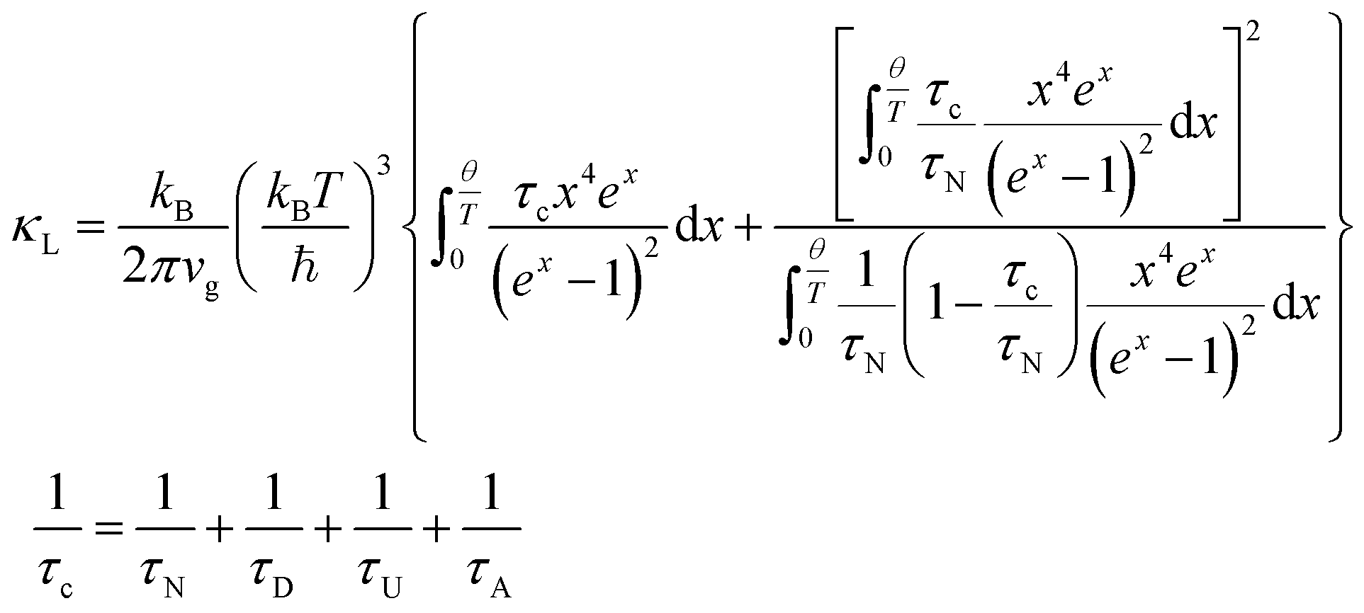
The thermal properties are plotted in Fig. 5. The thermal conductivities of the C60/Cu2Se nanocomposites were less than that of pure Cu2Se over the entire tested temperature range. Both electron thermal conductivities and lattice thermal conductivities were reduced for all C60/Cu2Se nanocomposites compared to those of pure Cu2Se. The reduction of electronic thermal conductivities is caused by reduction of electrical conductivities which are shown in Fig. 4(a). The lattice thermal conductivity reduction is due to phonon scattering by embedded C60 nanoparticles, and can be calculated by a relaxation time approximation:4,28
 | (3) |
 | ||
| Fig. 5 Thermal properties of C60/Cu2Se nanocomposites. Experimental (markers) and calculated (solid lines) (a) total thermal conductivities, (b) electron thermal conductivities, and (c) lattice thermal conductivities.38 | ||
The experimental and calculated lattice thermal conductivities are plotted in Fig. 5(c) (calculation details are described in the ESI.†) The phonon scattering by embedded C60s was considered to be defect scattering. The calculation was only based on the 0.7 mol% C60/Cu2Se nanocomposite sample. The volume fraction of C60 is derived from the mole fraction and size of C60. The calculation results fit well with the experimental results of the 0.7 mol% C60/Cu2Se nanocomposite. To fit the experimental data, 8 nm was used as the diameter of the clustered C60 nanoparticles, which is consistent with TEM results shown in Fig. 2. The samples with other C60 amounts (0.03, 0.3, 0.5 mol%) also had low lattice thermal conductivities that were similar to that of the 0.7 mol% sample. These data indicate that additional phonon scattering can drastically reduce lattice thermal conductivity when C60 is embedded in Cu2Se. For example, correlated scattering between scattered phonons by multiple C60 nanoparticles could additionally reduce lattice thermal conductivity.4 M. Brewster and C. Tien37 suggested that when c/λ < 0.3, where c is the interparticle distance and λ is the phonon wavelength, the correlated scattering effect should be considered, as interference between scattered phonons becomes important. A rough estimation (as described in the ESI†) suggests that the interparticle distances for the 0.3, 0.5, and 0.7 mol% C60/Cu2Se nanocomposites were around 5.3, 4.5, and 4.0 nm, respectively. As shown in Fig. 2, the experimentally observed value for interparticle distances was also on the few-nm scale. Considering that the dominant phonon wavelength is around 1–10 nm, some portion of phonon waves could have a c/λ value below 0.3, indicating the importance of the correlated scattering effect. Therefore, the observed lattice thermal conductivity is lower than the theoretical estimate, as shown in Fig. 5(c). Because of significant phonon scattering, the lattice thermal conductivity was around 0.25 W m−1 K−1 which is similar to the minimum thermal conductivity.2
As shown in Fig. 6, the maximum zT was around 1.4 at 773 K for the 0.7 mol% C60/Cu2Se nanocomposite. The enhancement of zT was mainly caused by the synergetic effect of phonon scattering and carrier localization. The strong phonon scattering by embedded C60 significantly reduced lattice thermal conductivity by 40–50% over the entire tested temperature range. The energy-dependent electron scattering by potential well of C60 significantly reduces electrical conductivity, resulting in the reduction of electronic thermal conductivity. Through these mechanisms, incorporation of C60 decreases the total thermal conductivity by around 60%. Moreover, the Seebeck coefficient is enhanced by the carrier localization. By the synergetic effect of the carrier localization and phonon scattering by the embedded C60s, zT is enhanced by 20–30% in C60/Cu2Se nanocomposites compared to that of pure Cu2Se.
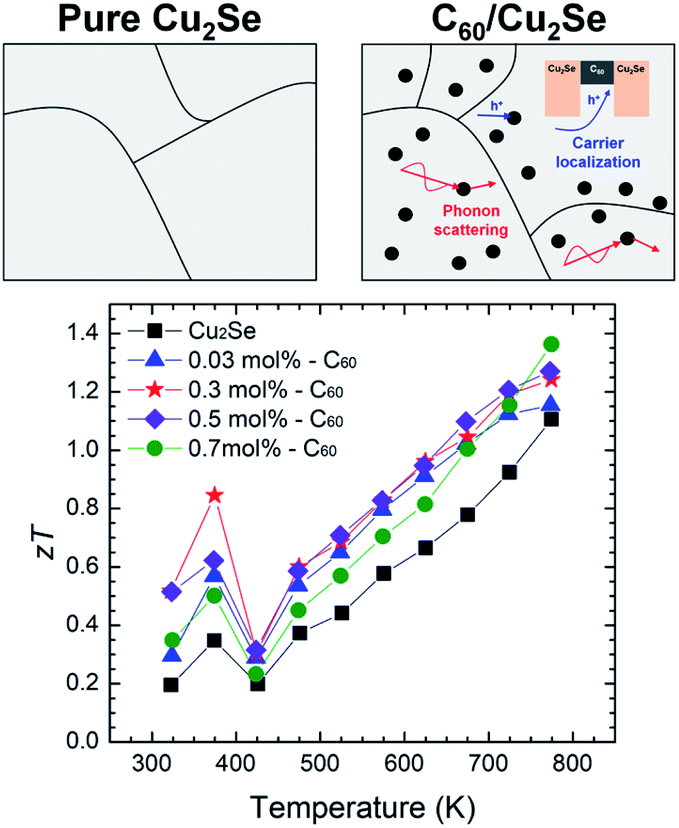 | ||
| Fig. 6 Schematic comparing pure Cu2Se and a C60/Cu2Se nanocomposite and the thermoelectric figure of merit zT as a function of temperature.38 | ||
Conclusion
C60 incorporated Cu2Se nanocomposites were synthesized using a simple solid-state reaction. The microstructure of the C60/Cu2Se nanocomposites was different from that of pure Cu2Se. Grain growth was suppressed in C60/Cu2Se nanocomposites because of the Zener pinning effect, showing that the nanocomposites contain more grain boundaries than pure Cu2Se. The dispersed C60s are clustered in the fullerite form around 10 nm size. They act as phonon scatterers and potential wells for holes. Due to the phonon scattering by the embedded C60 nanoparticles, the lattice thermal conductivity of the C60/Cu2Se nanocomposite is reduced by around 40–50% compared to that of pure Cu2Se. The reduction of lattice thermal conductivity was analyzed quantitively using a phonon scattering model. The Seebeck coefficient was enhanced by carrier localization caused by C60. Due to the difference in Fermi level between C60 and Cu2Se, C60 can act as a potential well for carriers (holes), resulting in carrier localization (energy filtering). Through quantitative analysis using the Boltzmann transport equation, it was found that the C60/Cu2Se nanocomposites have an additional scattering process for carriers that is caused by the C60 nanoparticles. The additional scattering process increased the Seebeck coefficient by 43%. Through the synergetic effect of phonon scattering and carrier localization in C60/Cu2Se nanocomposites, the thermoelectric figure of merit was enhanced by 20–30% compared to that of pure Cu2Se.Experimental38
Synthesis
The precursor materials, namely, copper powder (Cu, <425 μm, 99.5%), selenium pellets (Se, <5 mm, >99.99%), and fullerene powder (C60, 98%) were obtained from Sigma-Aldrich. The mixture of raw materials was sealed in a quartz tube and loaded in a furnace, where the temperature was slowly increased to 673 K in 6 hours and then held for 2 hours. The reaction was carried out at a temperature of 1073 K for 5 days, and the samples were naturally cooled to 298 K. Subsequently, the resultant ingots were ground into a powder. The fullerene (C60) was added to the as-synthesized Cu2Se powder through a simple mechanical alloy method. Fullerenes and hand ground Cu2Se were weighed to produce accurate C60 contents of 0.03, 0.3, 0.5, and 0.7 mol%. Then, the mixed powders were mechanically ground using planetary ball milling for 2 hours. The pure Cu2Se hand ground powder was also ground again using ball milling for 2 hours. In order to obtain high density samples for measurement, the ball-milled powders were consolidated into pellets by spark plasma sintering (SPS) at 723 K and under a high pressure of 85 MPa. The relative densities of C60-incorporated Cu2Se samples were 98.6–99.9% of the theoretical density.Characterization
The crystal structures of the ball-milled products and sintered pellets were characterized by powder X-ray diffraction (PXRD), recorded on X-ray diffractometer equipment using a Cu-Kα radiation wavelength of 1.5418 Å at 40 kV and 30 mA. The diffraction data were collected at a scan rate of 2° min−1 with the angle ranging from 10° to 80°. The microstructures of samples were obtained by scanning electron microscopy (SEM) using a JEOL JSM-6700F at an accelerating voltage of 10 kV. Transmission electron microscopy (TEM) and high resolution TEM (HR-TEM) images were recorded on a JEOL JEM-F200 instrument.The electrical conductivity (σ) and Seebeck coefficient (S) were measured simultaneously on a ZEM-3 (Ulvac-Riko ZEM-3). The thermal conductivity (κ) was obtained through κ = D × Cp × ρ, where D, Cp and ρ are the thermal diffusivity, heat capacity, and mass density, respectively. The thermal diffusivity (D) was measured using an LFA 457 (NETZSCH). The heat capacity (Cp) was obtained from the literature.36 The Archimedes method was performed to calculate the mass density (ρ). The Hall coefficient was obtained using a physical property measurement system (PPMS 16T, Quantum Design) with magnetic field ranging from −9 T to 9 T.
Calculation of Seebeck coefficient and lattice thermal conductivity
The calculation of the Seebeck coefficient is based on eqn (2) in the main text. The temperature-dependence of the Fermi level position is used as fitting parameter to calculate the Seebeck coefficient of pure Cu2Se. The Seebeck coefficient for C60/Cu2Se nanocomposites is fitted by changing the scattering parameter.The calculation of lattice thermal conductivity is based on the Callaway model, as described in eqn (3). The relaxation time for the defect (embedded C60) is obtained by methods reported in the literature.3 (A detailed process is described in the ESI.†)
Conflicts of interest
There are no conflicts to declare.Acknowledgements
This work was supported by the National Research Foundation of Korea (NRF) grant funded by the Korea government (MSIT) (NRF-2018R1A2B2005455).References
- D. M. Rowe, CRC Handbook of Thermoelectrics, CRC Press, 1995 Search PubMed.
- G. Chen, Nanoscale Energy Transport and Conversion, Oxford university press, New york, 2005 Search PubMed.
- W. Kim and A. Majumdar, J. Appl. Phys., 2006, 99, 084306 CrossRef.
- W. Kim, J. Zide, A. Gossard, D. Klenov, S. Stemmer, A. Shakouri and A. Majumdar, Phys. Rev. Lett., 2006, 96, 045901 CrossRef PubMed.
- W. Kim, R. Wang and A. Majumdar, Nano Today, 2007, 2, 40–47 CrossRef.
- K. Biswas, J. He, Q. Zhang, G. Wang, C. Uher, V. P. Dravid and M. G. Kanatzidis, Nat. Chem., 2011, 3, 160–166 CrossRef CAS PubMed.
- K. Biswas, J. Q. He, G. Y. Wang, S. H. Lo, C. Uher, V. P. Dravid and M. G. Kanatzidis, Energy Environ. Sci., 2011, 4, 4675–4684 RSC.
- J. He, J. Androulakis, M. G. Kanatzidis and V. P. Dravid, Nano Lett., 2011, 12, 343–347 CrossRef PubMed.
- L. D. Zhao, J. Q. He, C. I. Wu, T. P. Hogan, X. Y. Zhou, C. Uher, V. P. Dravid and M. G. Kanatzidis, J. Am. Chem. Soc., 2012, 134, 7902–7912 CrossRef CAS PubMed.
- L. D. Zhao, J. Q. He, S. Q. Hao, C. I. Wu, T. P. Hogan, C. Wolverton, V. P. Dravid and M. G. Kanatzidis, J. Am. Chem. Soc., 2012, 134, 16327–16336 CrossRef CAS PubMed.
- A. Banik and K. Biswas, J. Mater. Chem. A, 2014, 2, 9620–9625 RSC.
- H. Wang, J.-H. Bahk, C. Kang, J. Hwang, K. Kim, J. Kim, P. Burke, J. E. Bowers, A. C. Gossard, A. Shakouri and W. Kim, Proc. Natl. Acad. Sci. U. S. A., 2014, 111, 10949–10954 CrossRef CAS PubMed.
- W. H. Nam, B. B. Kim, Y. S. Lim, K. S. Dae, W. S. Seo, H. H. Park and J. Y. Lee, Nanoscale, 2017, 9, 12941–12948 RSC.
- K. Q. Zhang, H. C. Wang, W. B. Su, T. Wang, X. Wang, T. T. Chen, T. C. Huo, F. Dang, M. Y. Dong, C. L. Wang, B. B. Dong and Z. H. Guo, J. Phys. D: Appl. Phys., 2020, 53, 245501 CrossRef CAS.
- D. Narducci, E. Selezneva, G. Cerofolini, S. Frabboni and G. Ottaviani, J. Solid State Chem., 2012, 193, 19–25 CrossRef CAS.
- M. Zebarjadi, K. Esfarjani, M. S. Dresselhaus, Z. F. Ren and G. Chen, Energy Environ. Sci., 2012, 5, 5147–5162 RSC.
- J. H. Yingshi Jin, H. Mi-Kyung, W. Shon, R. Jong-Soo and K. Sung-Jin, ACS Appl. Mater. Interfaces, 2020, 12, 36589–36599 CrossRef PubMed.
- H. L. Liu, X. Shi, F. F. Xu, L. L. Zhang, W. Q. Zhang, L. D. Chen, Q. Li, C. Uher, T. Day and G. J. Snyder, Nat. Mater., 2012, 11, 422–425 CrossRef CAS PubMed.
- H. L. Ping Lu, X. Yuan, F. Xu, X. Shi, K. Zhao, W. Qiu, W. Zhang and L. Chen, J. Mater. Chem. A, 2015, 3, 6901–6908 RSC.
- H. L. Liu, X. Yuan, P. Lu, X. Shi, F. F. Xu, Y. He, Y. S. Tang, S. Q. Bai, W. Q. Zhang, L. D. Chen, Y. Lin, L. Shi, H. Lin, X. Y. Gao, X. M. Zhang, H. Chi and C. Uher, Adv. Mater., 2013, 25, 6607–6612 CrossRef CAS PubMed.
- B. Yu, W. S. Liu, S. Chen, H. Wang, H. Z. Wang, G. Chen and Z. F. Ren, Nano Energy, 2012, 1, 472–478 CrossRef CAS.
- B. Zhong, Y. Zhang, W. Q. Li, Z. R. Chen, J. Y. Cui, W. Li, Y. D. Xie, Q. Hao and Q. Y. He, Appl. Phys. Lett., 2014, 105, 123902 CrossRef.
- M. Li, D. L. Cortie, J. X. Liu, D. H. Yu, S. M. K. N. Islam, L. L. Zhao, D. R. G. Mitchell, R. A. Mole, M. B. Cortie, S. X. Dou and X. L. Wang, Nano Energy, 2018, 53, 993–1002 CrossRef CAS.
- R. Q. Zhang, Y. Q. Feng, S. T. Lee and C. L. Bai, J. Phys. Chem. B, 2004, 108, 16636–16641 CrossRef CAS.
- S. M. Lee, R. J. Nicholls, D. Nguyen-Manh, D. G. Pettifor, G. A. D. Briggs, S. Lazar, D. A. Pankhurst and D. J. H. Cockayne, Chem. Phys. Lett., 2005, 404, 206–211 CrossRef CAS.
- V. A. Kulbachinskii, V. G. Kytin, M. Y. Popov, S. G. Buga, P. B. Stepanov and V. D. Blank, J. Solid State Chem., 2012, 193, 64–70 CrossRef CAS.
- D. G. Zhao, J. A. Ning, D. Wu and M. Zuo, Materials, 2016, 9, 629 CrossRef PubMed.
- W. Kim, S. L. Singer, A. Majumdar, J. M. O. Zide, D. Klenov, A. C. Gossard and S. Stemmer, Nano Lett., 2008, 8, 2097–2099 CrossRef CAS PubMed.
- S. V. Faleev and F. Leonard, Phys. Rev. B: Condens. Matter Mater. Phys., 2008, 77, 214304 CrossRef.
- A. Pakdel, Q. S. Guo, V. Nicolosi and T. Mori, J. Mater. Chem. A, 2018, 6, 21341–21349 RSC.
- G. Couturier, R. Doherty, C. Maurice and R. Fortunier, Acta Mater., 2005, 53, 977–989 CrossRef CAS.
- D. K. Chen, T. Ghoneim and Y. Kulkarni, Appl. Phys. Lett., 2017, 111 CAS.
- J. I. Tapia, E. Larios, C. Bittencourt, M. J. Yacaman and M. Quintana, Carbon, 2016, 99, 541–546 CrossRef CAS.
- M. D. L. Gulay, O. Strok and A. Pietraszko, Chem. Met. Alloys, 2011, 4, 200–205 CrossRef.
- S. Ballikaya, H. Chi, J. R. Salvador and C. Uher, J. Mater. Chem. A, 2013, 1, 12478–12484 RSC.
- R. Nunna, P. F. Qiu, M. J. Yin, H. Y. Chen, R. Hanus, Q. F. Song, T. S. Zhang, M. Y. Chou, M. T. Agne, J. Q. He, G. J. Snyder, X. Shi and L. D. Chen, Energy Environ. Sci., 2017, 10, 1928–1935 RSC.
- M. Q. Brewster and C. L. Tien, J. Heat Transfer, 1982, 104, 573–579 CrossRef CAS.
- Y. Jin, Synthesis and Characterization of Cu2Se-based Nanostructured Materials and Their Thermoelectric Properties, Ewha Womas University, 2020 Search PubMed.
- T. Chen, H. Wang, W. Su, X. Wang, F. Mehmood, K. Zhang, T. Huo and C. Wang, Thermoelectric performance of Dy/Y co-doped SrTiO3 ceramic composites with submicron A2Ti2O7 (A = Dy, Y) pyrochlore, J. Phys. D: Appl. Phys., 2021, 54(15), 155501 CrossRef CAS.
- X. Wang, H. Wang, W. Su, T. Wang, M. A. Madre, J. Zhai, T. Chen, A. Sotelo and C. Wang, A novel multilayer composite structured thermoelectric module with high output power, J. Mater. Chem. A, 2020, 8, 3379–3389 RSC.
Footnotes |
| † Electronic supplementary information (ESI) available. See DOI: 10.1039/d1na00085c |
| ‡ These authors equally contributed to this work. |
| This journal is © The Royal Society of Chemistry 2021 |