
 Open Access Article
 This Open Access Article is licensed under a Creative Commons Attribution-Non Commercial 3.0 Unported Licence
Surface passivation of organometal halide perovskites by atomic layer deposition: an investigation of the mechanism of efficient inverted planar solar cells†
Ran
Zhao‡
 a,
Kai
Zhang‡
b,
Jiahao
Zhu‡
a,
Shuang
Xiao
*b,
Wei
Xiong
a,
Jian
Wang
b,
Tanghao
Liu
c,
Guichuan
Xing
c,
Kaiyang
Wang
c,
Shihe
Yang
*b and
Xinwei
Wang
*a
a,
Kai
Zhang‡
b,
Jiahao
Zhu‡
a,
Shuang
Xiao
*b,
Wei
Xiong
a,
Jian
Wang
b,
Tanghao
Liu
c,
Guichuan
Xing
c,
Kaiyang
Wang
c,
Shihe
Yang
*b and
Xinwei
Wang
*a
aSchool of Advanced Materials, Shenzhen Graduate School, Peking University, Shenzhen 518055, China. E-mail: wangxw@pkusz.edu.cn
bGuangdong Key Lab of Nano-Micro Material Research, School of Chemical Biology and Biotechnology, Shenzhen Graduate School, Peking University, Shenzhen 518055, China. E-mail: xiaoshuang@pku.edu.cn; chsyang@pku.edu.cn
cInstitute of Applied Physics and Materials Engineering, University of Macau, Avenida da Universidade, Taipa, Macau, China
First published on 18th February 2021
Abstract
Interface passivation plays a pivotal role in achieving high-efficiency organic metal halide perovskite solar cells (PSCs). It has been recently revealed that atomic layer deposition (ALD) of wide-band gap oxides shows great potential to effectively passivate defects at the interface, and ALD is also of great technological promise for industrial upscaling. However, the conflicting observations of ALD passivation are often reported in the literature, even with very similar ALD conditions. To unveil the involved crucial mechanism, this work carefully investigates the evolution of a representative MAPbI3 perovskite surface during the ALD of Al2O3, by employing the technique of in situ X-ray photoelectron spectroscopy. The ALD at 125 °C was found to cause significant degradation of the perovskite; lowering the deposition temperature can largely minimize the degradation, and 75 °C was found to be the best ALD temperature. Following this conclusion, inverted planar perovskite solar cells were prepared in ambient conditions with ALD Al2O3 interlayers. Indeed, cells with the interlayer deposited at 75 °C exhibited a significantly enhanced power conversion efficiency from 18.8% (champion 19.2%) to 20.0% (champion 20.4%). Photoluminescence measurements further evidence that the ALD layer can effectively passivate defect states at the perovskite surface. Considering the great representativeness and broad applicability of MAPbI3 and ALD Al2O3, the mechanism and strategy reported herein should be of significant value for the perovskite interface engineering in general.
Introduction
Organic–inorganic halide perovskite solar cells (PSCs) are highly promising emerging photovoltaic cells, and they have shown rapid improvement in certified power conversion efficiency (PCE) from 3.8% to 25.5% over the past decade.1,2 While the halide perovskites appear to be resilient to bulk point defects (such as vacancies, interstitials, and antisites), their optoelectronic properties are fairly susceptible to the quality of perovskite (PVK) surfaces and interfaces.3 Given current synthesis techniques, perovskite surfaces are rarely stoichiometric and usually defective.3 Defects at perovskite surfaces could induce significant nonradiative charge recombination and deteriorate the solar cell performance.3–7 Particularly, in state-of-the-art solar cells, the nonradiative recombination at interfaces between the perovskite and charge transport layers is predominant compared to those in the bulk or at grain boundaries.4 Therefore, the passivation of interface defects is pivotal to achieve high-efficiency PSCs. To this end, numerous passivation approaches have been reported, for instance, by adding an interlayer of small molecules, polymers, and inorganic compounds or incorporating wide-band gap 2D perovskites.8–11 Despite their promising improvements on solar cell efficiency, concerns still remain about the upscalability of these approaches.Recently, atomic layer deposition (ALD) of wide-band gap oxides (e.g. Al2O3) has emerged as a promising strategy to effectively passivate perovskite surfaces.12 ALD is a scalable vapor-phase thin-film deposition technique, which relies on sequential alternate self-limiting surface reactions, and it is renowned for producing highly uniform, conformal thin films on non-flat surfaces with atomic-precise film thickness control and remarkable process reproducibility.13,14 Currently, ALD has been widely used in the Si photovoltaic industry for the production of passivated emitter and rear cells (PERC).15 Analogously, the passivation of perovskites by ALD is of great technological promise for future industrial upscaling. However, despite a number of positive reports showing promising improvements in the efficiency and stability of PSCs, direct growth of ALD on the top of perovskites has often encountered significant incompatibility issues.12,16,17 During an ALD process, perovskites are subjected to an often elevated temperature and the exposures of ALD precursors could potentially change the structure, composition, and therefore the optoelectronic properties of perovskites. Notably, these effects are largely dependent on the ALD surface reaction chemistries and the properties of perovskites (such as composition and surface condition).12,16,17 Hence, understanding the fundamental mechanisms of the interactions between ALD precursors and perovskites becomes the key to reliably employing this ALD technology for PSCs. Toward this goal, a growing number of reports have recently appeared to investigate the related ALD mechanisms, but often conflicting observations were published in the literature.12 For instance, taking the most studied system of ALD Al2O3 on methylammonium lead iodide (MAPbI3) as an example, under quite similar deposition conditions, both increase and decrease in the solar cell efficiency have been reported.18–26 Notably, a recent study27 using in situ quartz crystal microbalance (QCM) and quadruple mass spectrometry (QMS) showed that the differences in the ALD temperature and precursor partial pressure could result in drastically different outcome interfaces, which were suggested to account for the discrepancies observed across different laboratories. Their conclusion, together with the well-known sensitivity of the perovskite surfaces and subtleties in preparation, highlights two very important issues for this type of studies. First, the mechanism study should be accompanied with the high-reliability and high-performance PSCs; otherwise, the conclusions do not reflect the de facto limiting factors. Second, the mechanism study should be conducted in situ or in vacuo, in order to avoid possible ambient interference when exposed to air.
To find out the critical mechanism underlying ALD passivation, we herein focused on the PSCs with high benchmarking PCE (18.8% in average) and employed the technique of in situ X-ray photoelectron spectroscopy (XPS) to investigate the evolution of the perovskite surface during the ALD process. The representative perovskite of MAPbI3 and the ALD material of Al2O3 were chosen for this study. Following the careful study, we found that quite a few experimental observations were rather different from previous reports, which highlight the importance of carrying out in situ investigation on high-efficiency PSCs. Therefore, the results and mechanism reported herein should be of significant value for the interface engineering of high-performance PSCs in general.
Experimental
Materials
Fluorine-doped tin oxide (FTO, 1.5 cm × 1.5 cm) was purchased from OPV TECH LTD. Methylammonium iodide (MAI) was purchased from Dyesol Ltd. Lead iodide (PbI2, extra dry, 99.999%) and nickel(II) acetylacetonate (95%) were purchased from Alfa Aesar Ltd. N,N-Dimethylformamide (DMF, anhydrous, 99.8%), dimethyl sulfoxide (DMSO, anhydrous, 99.8%) and chlorobenzene (CB, extra dry, 99.5%) were purchased from Acros Ltd. 2,2,2-Trifluoroethanol (TFE, 99.5%) was purchased from Energy chemical Ltd. [6,6]-Phenyl-C61-butyric acid methyl ester (PC61BM) was purchased from NANO-C Tech Ltd. Anisole (anhydrous, 99.7%) was purchased from Aladdin Ltd. Diethanol amine (DEA, 99%) was purchased from Sigma-Aldrich Ltd.Device fabrication
The perovskite precursor solution was prepared according to our previous publications.28,29 First, 461 mg of PbI2 and 159 mg of MAI were dissolved in a mixture of 434 μL DMSO and 124 μL DMF. After stirring on a 60 °C hotplate overnight, the transparent yellowish solution was filtered using a filter head of 0.22 μm. A perovskite film was prepared using the as-prepared solution in a fume hood under the humidity between 20 and 60% RH. Then, 35 μL of the as-prepared precursor solution was drop-casted onto the substrate at room temperature. The spin coating process consisted of four steps, which were 1000 rpm for 45 s, 6000 rpm for 40 s, 0 rpm for 10 s, and 6000 rpm for 10 s sequentially. During the last 5 s of the second step and the whole process of the fourth step, 80 μL anisole was dropped onto the substrate, respectively. After the first dripping, the film was still transparent and it could maintain the state for a long time in ambient air. After the second dripping, the film turned brown in color, and the as-prepared film was converted into a compact perovskite film at room temperature or 98 °C for 7 min in an ambient atmosphere. On top of the perovskite film, atomic layer deposition (ALD) of Al2O3 was carried out under different conditions.
The PC61BM solution (20 mg mL−1 in CB) was fabricated and stirred at 60 °C for 2 h. First, 35 μL of PC61BM solution was drop-casted onto the substrate and spun at 3000 rpm for 30 s. The interface material PPDIN6 was synthesized according to our previous publication.11 The PPDIN6 solution (0.5 mg mL−1 in TFE) was fabricated and stirred overnight at room temperature. Then, 40 μL of PPDIN6 solution was drop-casted onto the substrate and spun at 3000 rpm for 30 s. Finally, 150 nm of Ag electrode was evaporated on top.
Characterization
 , where λ (=2.3 nm (ref. 34)) is the effective attenuation length of the photoelectrons in the Al2O3 layer, θ (=90°) is the photoelectron take off angle, IAl 2p and II 3d are the measured intensities of the Al 2p and I 3d signals from the substrate, respectively, and β (=I∞Al 2p/I∞I 3d) is the ratio of the Al 2p and I 3d intensities for thick Al2O3 and perovskite substrates.
 ,
,  , where A1 and A2 are the relative amplitudes and τ1, τ2, and τave are the fast, slow, and average decay lifetimes, respectively.
Results and discussion
In situ XPS was employed to monitor the evolution of the MAPbI3 perovskite surface upon the ALD of Al2O3 from trimethylaluminum (TMA) and H2O (Fig. 1a). Three representative ALD temperatures of 25 °C, 75 °C and 125 °C were selected to investigate the temperature effect. As a few recent reports27,35 suggested that the MAPbI3 perovskite could be etched by excessively exposing to the TMA and H2O vapors, we chose to use relatively small exposures of 0.025 and 0.051 Torr s for the TMA and H2O vapors, respectively, in each ALD cycle. These exposures were sufficient to saturate the normal ALD growth of Al2O3 on the flat SiOx surface.36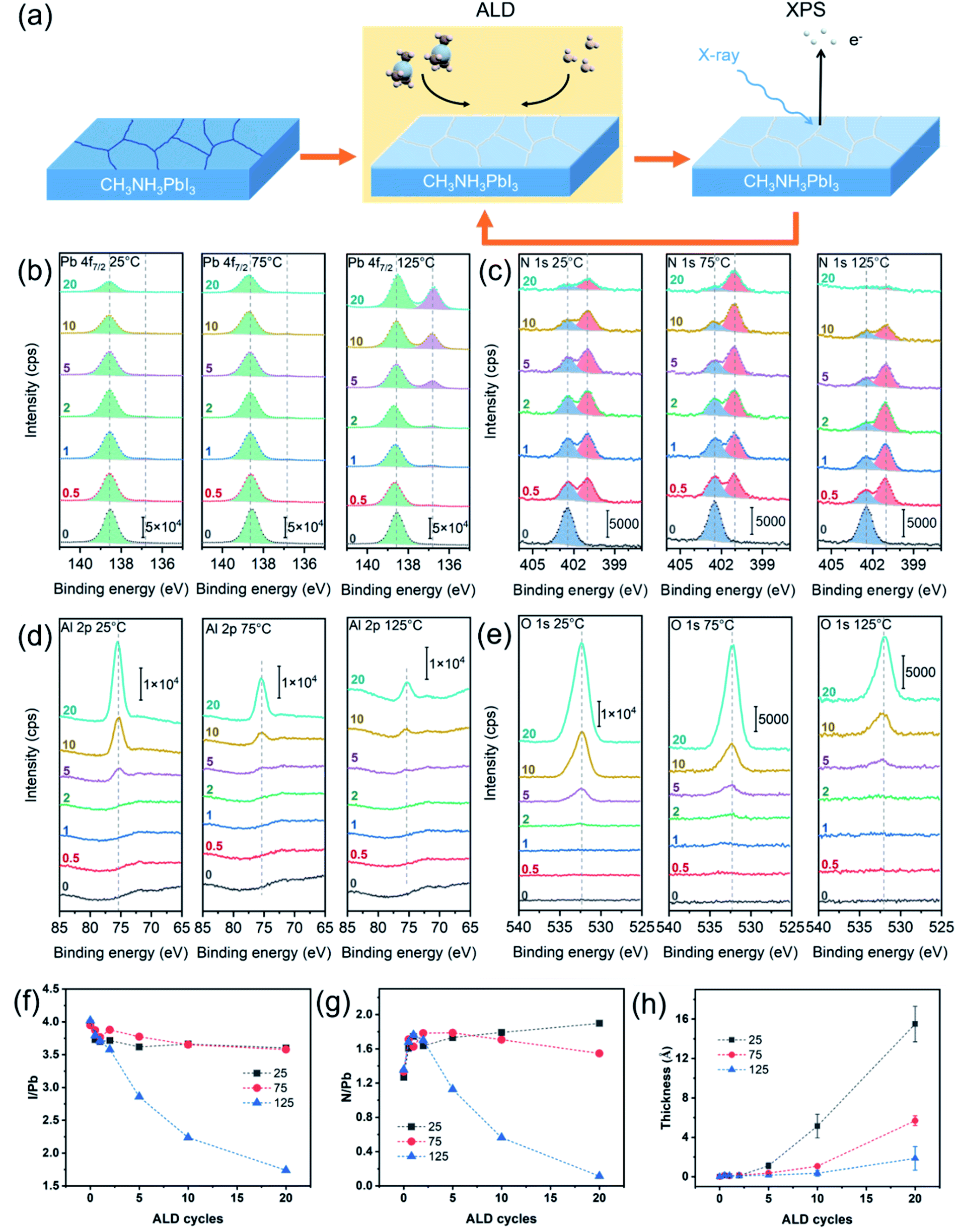 | ||
| Fig. 1 (a) Schematic of the in situ experimental procedure. High-resolution XPS core-level spectra of (b) Pb 4f7/2, (c) N 1s, (d) Al 2p, and (e) O 1s taken from 0 cycles (i.e., initial surface) through 20 cycles of ALD of Al2O3 on MAPbI3. The deposition temperatures were 25 °C, 75 °C and 125 °C. Atomic ratios of (f) I/Pb and (g) N/Pb and (h) the equivalent thickness of the deposited Al2O3 with respect to the number of the ALD cycles. | ||
Fig. 1b–e shows the acquired in situ XPS spectra for the core-level emissions of Pb 4f7/2, N 1s, Al 2p, and O 1s. All the XPS spectra were taken for 0 cycle (i.e., initial surface) through 20 cycles of Al2O3 deposited on the perovskite surface. Half-integer and full-integer numbers were used to denote the spectra taken after the TMA and H2O half-cycles, respectively. Fig. 1b compares the evolutions of the Pb 4f7/2 spectra upon the ALD at 25, 75 and 125 °C. All the spectra for the pristine perovskite surfaces (0 cycle) show a similar symmetric peak at a binding energy (BE) of 138.6 eV, which corresponds to Pb2+–I in perovskites.37 However, as the ALD proceeded, the Pb 4f7/2 spectra behaved differently for the depositions at different temperatures. At a low deposition temperature of 25 °C or 75 °C, the intensity of the Pb2+–I peak continually diminished as the deposition proceeded, probably owing to the increasing attenuation of the photoelectrons by the deposited Al2O3 layer on top. Comparatively, the signal diminished faster for 25 °C than 75 °C, suggesting a faster per-cycle growth of Al2O3 at 25 °C. As for the ALD at 125 °C, the Pb 4f7/2 spectrum continually developed an additional peak at a lower BE of 136.8 eV, and this BE corresponds to metallic lead (Pb0),37 which suggests that the Pb2+ in perovskite was reduced upon the ALD at 125 °C. Considering that the conduction band minimum of MAPbI3 has mostly nonbonding Pb p character,38 the reduction of Pb2+ to Pb0 can significantly alter the optoelectronic properties of MAPbI3. Perhaps because it was only present on the surface and of a small amount compared to the bulk, the metallic lead was not observed by XRD or IR in previous ALD studies,18,35,39 and thus its adverse effect on the solar cell performance was likely overlooked. In addition, it is worth noting that no Pb–OH species (at 138.2 eV (ref. 20)) was detected on the pristine perovskite surfaces or after the ALD, and this observation is in stark contrast to a previous study on relatively low-PCE (13.6%) MAPbI3 surface,20 which therefore signifies a different passivation mechanism for high-PCE MAPbI3 surfaces.
Fig. 1c compares the evolutions of the N 1s spectra upon the ALD at 25, 75 and 125 °C. All the spectra of the pristine perovskite surfaces show a single peak at 402.4 eV for N in CH3NH3+,37 but after the TMA dose, a pronounced new peak emerged at a lower BE of 401.0 eV. The appearance of this peak is suggestive of the deprotonation of CH3NH3+ by TMA to afford CH3NH2,35,40 which has a lower N 1s BE.41,42 Although CH3NH2 itself is a gas at room temperature (b.p. −6.8 °C), for the ALD at ≤75 °C, most of the afforded CH3NH2 seemed to remain in the perovskite or be trapped at the perovskite/Al2O3 interface. In contrast, the ALD at 125 °C resulted in a significant reduction of the overall N 1s signal (e.g. 20 cycles), which indicates a significant loss of CH3NH3+ at 125 °C.
Fig. 1d and e displays the acquired Al 2p and O 1s spectra upon the ALD at 25, 75 and 125 °C. All the Al 2p spectra show a similar trend, where no Al 2p signal was observed for the first 2 cycles, indicating that the growth of ALD Al2O3 on the perovskite was delayed. After 5 ALD cycles, the spectra showed observable Al 2p peaks, and the peak intensities later increased as the ALD proceeded. The peak BE was found to be at 75.5 eV, which agrees with Al2O3 (Al–OH).21,43 The O 1s spectra showed correlated results that the O signals were barely observable after 2 cycles and became prominent (at 532.7 eV, Al–OH21,43) after 5 cycles, and these results corroborate that the ALD Al2O3 growth was delayed on the perovskite. It is worth noting that the O 1s spectra for the initial MAPbI3 surfaces do not contain any detectable O signals, which is in stark contrast to previous photoelectron spectroscopy studies.20,21 This discrepancy signifies different ALD growth behaviors, which could therefore lead to different passivation mechanisms for the perovskite solar cells. Nevertheless, the intensities of the Al 2p and O 1s peaks are correlated with the amount of the Al2O3 grown on the perovskite surface, and apparently the growth was slower at a higher temperature. In addition, I 3d5/2 spectra were also taken. As shown in Fig. S1,† aside from a continual signal intensity decrease with the ALD cycle number, all the I 3d5/2 spectra show only a single peak at 619.4 eV for Pb2+–I,37 and thus no iodate-like species (at 623.8 eV (ref. 44)) was formed.
Based on the above-mentioned in situ XPS results, the change in the perovskite surface composition was traced. Fig. 1f and g plot the atomic ratios of I/Pb and N/Pb extracted from the XPS spectra. Because the mean free path of the photoelectrons is about 2–3 nm,34 these ratios reflect only the compositional information near the perovskite surface. The I/Pb and N/Pb ratios for the pristine perovskite surfaces (e.g., 0 ALD cycle) were found to be 4.0 and 1.3, respectively. These numbers are greater than those in the stoichiometric MAPbI3, which suggests that the initial perovskite surface contained excessive iodine and MAI.45 Although the I-rich MAI surface termination is more stable than the PbI2 termination for the MAPbI3 surface,46–48 excessive iodine can result in deep electronic traps, thereby deteriorating the solar cell performance.49 Apparently, as shown in Fig. 1f, the surface reactions of the I-rich MAPbI3 with the ALD precursors of TMA and H2O can reduce the surface I/Pb ratio, by forming volatile CH3I, as previously identified via in situ QMS.27 As shown in Fig. 1f, the 10- and 20-cycle ALD at 25 °C or 75 °C reduced the I/Pb ratio to 3.7 and 3.6, respectively. As for the ALD at 125 °C, the I/Pb ratio drastically decreased to 2.2 and 1.7 after 10 and 20 ALD cycles, respectively, which is consistent with the formation of metallic Pb as previously suggested from the BE change. Concurrently, a significant drop of the N/Pb ratio to 0.1 was found for the 20-cycle ALD at 125 °C (Fig. 1g). Such a low N/Pb ratio indicates a significant loss of the CH3NH3+ ions, which eventually collapsed the perovskite structure to form PbI2 (as will be shown later). However, we also noticed a pronounced increase in the N/Pb ratio (from 1.3 to 1.7) upon the first TMA dose (0.5 cycle) for all the temperatures. Given the surface-sensitivity of the XPS technique, the increase in the N/Pb ratio suggests that a certain amount of CH3NH2 accumulated near the perovskite surface. CH3NH2 could be afforded at the perovskite surface and grain boundaries; for the latter, the afforded CH3NH2 diffused outward through the grain boundaries to the top of the perovskite layer. This situation is analogous to a technique called methylamine-induced defect-healing (MIDH), which aims to reduce the perovskite defects by recrystallizing it via an intermediate MAPbI3·xCH3NH2 liquid.50,51 Certainly, the in situ formed CH3NH2 in our case was only of a small amount and thus not enough to form a full liquid intermediate, but the defects at the surface can be healed by the same scheme. In addition, CH3NH2 can also passivate the surface I vacancies by coordinating to Pb2+, forming a Pb–N bond which is much stronger than Pb–OH.52
The thickness of the ALD Al2O3 layer can be estimated from the degree of attenuation of the photoelectron signal from the perovskite underneath (see Experimental). Fig. 1h plots the extracted equivalent Al2O3 thickness with respect to the ALD cycle number. For all the deposition temperatures, the initial Al2O3 growth was delayed for at least 2 cycles, and after 5 cycles, the thickness versus cycle number exhibited a superlinear relation, which suggests that the per-cycle growth rate accelerated as the deposition proceeded. This behavior is suggestive of an inhibited initial growth mechanism.53 Inhibited initial growth is usually because of the lack of ALD-reactive moieties on the substrate surface, and it would normally result in the growth of islands on the substrate.53 Given the small equivalent thickness of ALD-Al2O3 after 10 cycle ALD at 25–125 °C, the afforded Al2O3 islands should be no greater than several nanometers in size and therefore elude direct observation by SEM or AFM. Although detailed chemistry of the ALD Al2O3 growth on MAPbI3 is still unknown, the ALD Al2O3 growth normally starts from TMA reacting with surface hydroxyls to afford Al–O bonds. Presumably, the same reaction scheme is also plausible if the surface defect sites adsorb H2O. Recently, Choudhury et al.35 and Koushik et al.40 proposed another reaction scheme that TMA reacts with MAPbI3 to afford a PbI3–Al(CH3)2 complex; however, our XPS results did not show the presence of Al after the first TMA half-cycle. Therefore, the growth from the surface defect sites is more likely to be the case. Given that the surface defects are often detrimental to the perovskite optoelectronic properties,3,4 fine-tuning the ALD conditions to well passivate these defects is of crucial importance to achieve high-performance solar cells.
X-ray diffraction (XRD) was employed to investigate the bulk part of the perovskite upon ALD. Fig. 2a compares the obtained XRD patterns for the pristine perovskite and the perovskites with 10-cycle ALD Al2O3 grown at different temperatures. The pattern of the pristine perovskite contains the characteristic MAPbI3 diffraction peaks of (110) and (200) at 14.2° and 20.1°, respectively,18,54 and the pattern remained almost the same after the 10-cycle ALD at 25 °C or 75 °C. However, for the ALD at 125 °C, a prominent PbI2 (001) peak appeared at 12.8°, while the perovskite (110) peak became weaker. These results indicate that a considerable portion of the perovskite was converted to PbI2 upon the ALD at 125 °C. Notably, thermal annealing at 125 °C itself was not enough to drive this conversion, as the vacuum annealed sample shows an almost unchanged XRD pattern. Therefore, the surface reactions with the ALD precursors must be the promoter to the degradation of the perovskite structure. Scanning electron microscopic (SEM) measurements were performed to examine the morphology of the above perovskite samples. The pristine perovskite layer was found to be fairly smooth and uniform (Fig. 2b), and the surface morphology remained almost unchanged after the ALD at 25 °C or 75 °C (Fig. 2c and d) or by vacuum annealing at 125 °C (Fig. S3†). However, the ALD at 125 °C considerably roughened the surface and created pinholes through the perovskite layer (Fig. 2e). On the basis of the above-mentioned analysis, Fig. 2f schematically summarizes the evolutions of MAPbI3 upon the ALD of Al2O3 at different temperatures. While the ALD at 125 °C considerably roughened the perovskite surface and formed metallic lead and PbI2, the degradation was largely minimized as the ALD temperature was lowered to 25 or 75 °C. Compared to 25 °C, the initial ALD growth at 75 °C was apparently slower, and therefore, the growth could occur more selectively on the surface defects.55 As such, wide-band gap Al2O3 could be more selective to only passivate the surface defects while not to impede the charge transport across the interface. Therefore, 75 °C was determined to be the best ALD temperature for perovskite passivation. In order to compare the hydrophobicity of the MAPbI3 surface, we carried out the contact angle measurement. The contact angle increased from 52.79° to 75.81° after 10 cycles of ALD-Al2O3 at 75 °C (Fig. S4†), which indicates that the MAPbI3 surface became more hydrophobic after ALD of Al2O3.
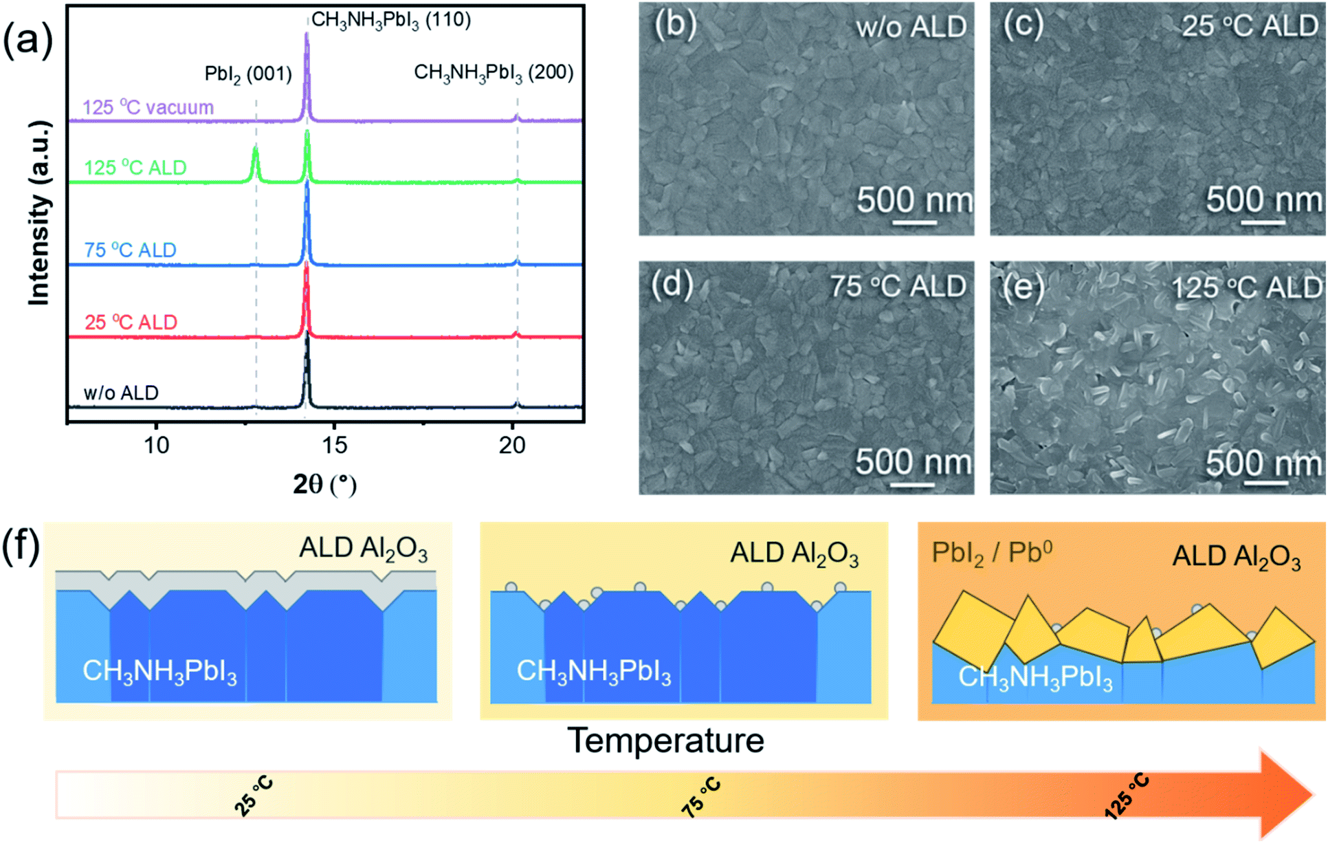 | ||
| Fig. 2 (a) XRD patterns and (b–e) SEM images taken on a pristine MAPbI3 film and the films with 10-cycle ALD of Al2O3 on top. The deposition temperatures were 25 °C, 75 °C and 125 °C. For comparison, the XRD pattern for a MAPbI3 film annealed under vacuum at 125 °C is also shown. (f) Schematic of the evolution of MAPbI3 upon the ALD of Al2O3 at different temperatures. | ||
To further demonstrate the ALD passivation effect, we fabricated a series of inverted planar MAPbI3 solar cells with ALD Al2O3 and measured their photovoltaic performance. The cells had a configuration of FTO/NiOx/MAPbI3/ALD-Al2O3/PCBM/PPDIN6/Ag, which is schematically shown in Fig. 3a. The influence of the ALD temperature was first investigated by 10-cycle ALD of Al2O3 directly on MAPbI3 (Fig. 3b). The benchmarking solar cells (i.e. without ALD) exhibited an average power conversion efficiency (PCE) of 18.8% (champion of 19.2%). The ALD at the temperatures of 25 °C and 75 °C were both found to increase the PCE. As shown in Fig. 3b and S2,† the open-circuit voltage (Voc) and fill factor were both increased by ALD, probably because of the surface defect passivation by the ALD of Al2O3. However, the variations in the PSC parameters are considerably larger for 25 °C than for 75 °C, which suggests that the ALD passivation at 25 °C is less stable. However, the ALD at 125 °C was found to drastically deteriorate the efficiency to 14.2%, probably by forming the more insulating PbI2 at the surface, which hindered the interface charge transfer and therefore reduced the short-circuit current (Jsc).
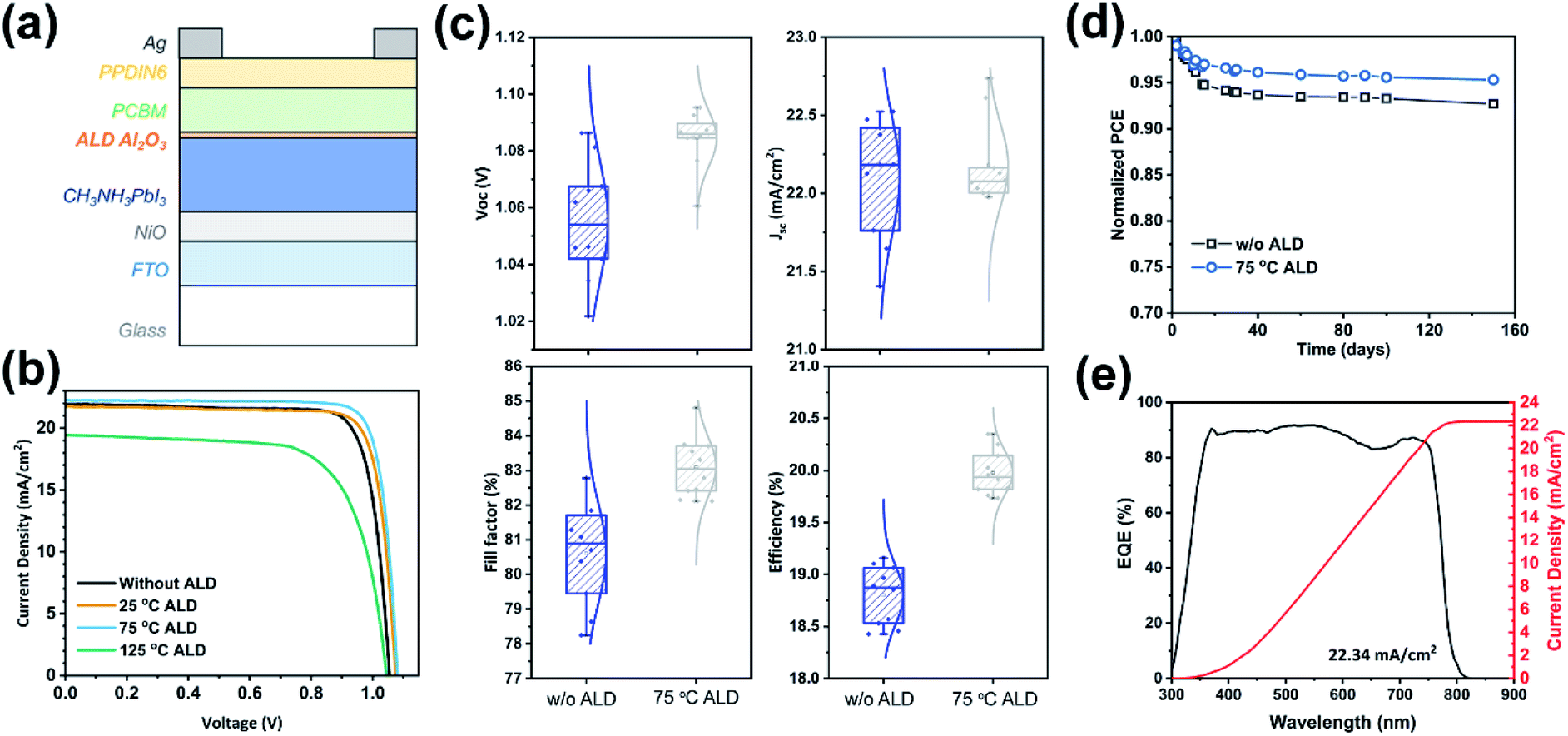 | ||
| Fig. 3 (a) Schematic architecture of the ambient-prepared PSCs with an ALD Al2O3 interlayer: FTO/NiOx/MAPbI3/ALD-Al2O3/PCBM/PPDIN6/Ag. (b) Curves of current density versus voltage (J–V) for the PSCs with and without 10 cycles of ALD of Al2O3 deposited at 25 °C, 75 °C and 125 °C, and the corresponding statistical distributions of performance parameters are shown in Fig. S2.† (c) Statistical distributions of Voc, Jsc, fill factor, and PCE for the PSCs with and without ALD Al2O3 deposited at 75 °C. (d) Long-term stability of PSCs in a N2 atmosphere. (e) Incident photon-to-electron conversion efficiency (IPCE) spectrum and the corresponding integrated current density for the PSCs with 10 cycles of ALD of Al2O3 at 75 °C ((b): 75 °C ALD). | ||
Given the optimal ALD temperature of 75 °C, the effect of the total ALD cycle number was also investigated. As shown in Fig. S5,† the cells with 10-cycle ALD of Al2O3 gave out the highest PCE, as compared to the 5- and 20-cycle samples. Notably, the equivalent thickness of 10-cycle ALD of Al2O3 was only about 1 Å (Fig. 1h). With this extremely small number, it is highly probable that ALD Al2O3 grew only selectively on the defect sites of the perovskite surface. This selective growth is desirable for effectively passivating the defects while not impeding the charge transport at the interface. As a result, 10-cycle ALD of Al2O3 75 °C gave out a much-improved average PCE of 20.0% and a champion PCE of 20.4% (Fig. 3c). Moreover, the hysteresis was small for both of the PSCs with and without 10 cycles of ALD of Al2O3 at 75 °C (Fig. S6†).
The stability of the fabricated solar cells was also evaluated in a N2-filled glove box. As shown in Fig. 3d, after the initial “burn-in” process,29,56 the normalized PCE of the solar cells remained fairly stable over the later test period up to 150 days. With the addition of ALD Al2O3, the eventual retention of the PCE increased from 92.7% to 95.3%, which suggests a good stability of the ALD-passivated perovskite. The maximum power point tracking result is shown in Fig. S7,† in which the PSCs with and without ALD-Al2O3 both have high operational stability. The incident photon-to-electron conversion efficiency (IPCE) spectrum was also measured for the ALD-passivated champion cell. As shown in Fig. 3e, the spectrum shows a rather flat plateau at ∼90% over the wavelength range from 380 to 760 nm, and the integrated current density was found to be 22.34 mA cm−2, which agrees well with the cell J–V curve of sample 75 °C ALD in Fig. 3b.
To further understand the charge transport at the perovskite/Al2O3 interface, we carried out both steady-state photoluminescence spectroscopy (PL) and time-resolved photoluminescence spectroscopy (TRPL) experiments on the perovskite films with PVK/Al2O3 and without ALD Al2O3 (PVK). The observed PL signals (Fig. 4a) reflect the radiative direct recombination of the photo-generated free carriers. With the presence of defects, the photo-generated carriers can be trapped at the defects and recombine non-radiatively via a Shockley–Read–Hall (SRH) process, resulting in poor PL efficiency.57,58 As shown in Fig. 4a, compared to the bare perovskite film, the perovskite with ALD Al2O3 shows appreciably enhanced PL intensity, which suggests that the defects at the MAPbI3 surface were well passivated by the ALD of Al2O3. At the same time, a small blue-shift from 768 to 766 nm was also observed for the PL peak of the PVK/Al2O3 sample, and this blue-shift could be well ascribed to the reduction of the defect traps, which recover the band edge transition.59,60 Reinforcing evidence was also obtained from the TRPL results. Fig. 4b and c show the TRPL spectra of the samples with the laser illumination from the air side (i.e. the Al2O3 side) and the glass side, respectively. Note that the light penetration depth (∼100 nm (ref. 61)) is smaller than the perovskite layer thickness, and therefore, the TRPL spectra of different sides can provide information about the location of the defects. As shown in Fig. 4b and c, the TRPL curves were all fitted by a bi-exponential decay function, where a longer lifetime of decay corresponds to fewer defects.4,62,63 Table S1† displays the detailed fitting results. For the air-side illumination, the average lifetime increases significantly from 20.88 ns to 73.39 ns after the ALD of Al2O3, which again suggests that the ALD of Al2O3 can effectively passivate the defects on the perovskite surface. In comparison, the glass-side TRPL curves give out a smaller increase in the average lifetime from 49.42 ns to 77.52 ns after the ALD. These results suggest that most of the problematic defects are located near the top surface of the perovskite and they can be effectively passivated by the ALD of Al2O3 (Fig. 4d).64
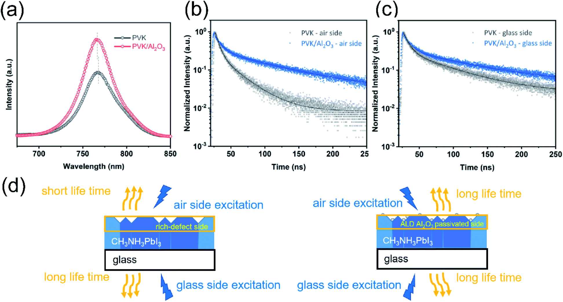 | ||
| Fig. 4 (a) Steady-state photoluminescence (PL) spectra and (b and c) time-resolved photoluminescence (TRPL) spectra of the perovskite-on-glass samples with and without ALD Al2O3. (d) Schematic of the relationship between the carrier life time and laser excitation side. | ||
Conclusions
In summary, the atomic layer deposition (ALD) technique offers a generally promising approach to effectively passivate the perovskite surface defects to improve the power conversion efficiency and stability of PSCs. However, owing to the sensitive chemical reactivity of the perovskite surface, discrepant and conflicting observations of the ALD passivation were often reported in the literature. To unveil the involved crucial mechanism, we herein utilized the in situ XPS technique to directly investigate the evolution of a representative high-performance MAPbI3 perovskite surface during the ALD process of Al2O3. For the ALD at 125 °C, we observed pronounced degradation of the perovskite, as there formed metallic lead at the perovskite/Al2O3 interface and a considerable portion of the bulk perovskite converted to PbI2. As the ALD temperature was lowered to 25 or 75 °C, the degradation was largely minimized, and we observed the formation of CH3NH2, which could possibly heal the perovskite surface defects. The initial ALD growth at 75 °C was apparently slower than that at 25 °C, and therefore Al2O3 grew more selectively on the surface defects, which was desirable to not impede the charge transport across the interface. Therefore, 75 °C was determined to be the best ALD temperature for perovskite passivation. Following this conclusion, inverted planar perovskite solar cells were prepared with the ALD interlayers. Indeed, the cells with the ALD Al2O3 interlayer deposited at 75 °C exhibited a significantly enhanced PCE from 18.8% (champion 19.2%) to 20.0% (champion 20.4%), along with improved Voc and fill factor. In contrast, the ALD at 125 °C drastically deteriorated the cell PCE, which signifies the crucial importance to restrain the in-ALD-process degradation of the perovskites for the high-performance PSCs. Finally, we carried out steady-state and time-resolved PL to explicitly characterize the perovskite layer, and the results indicated that it was the ALD layer that reduced the defect states at the perovskite surface. The harmony of the PSC performance with the implications from the mechanism investigation well highlights the importance of the in situ interface investigation toward rational designing of the perovskite solar cells. Considering the great representativeness and broad applicability of MAPbI3 and ALD Al2O3, the mechanism and strategy reported herein should be of significant value for the PSC interface engineering in general.Author contributions
R. Zhao, K. Zhang, and J. Zhu contributed equally to this work. Prof. S. Yang, S. Xiao and X. Wang supervised this work. R. Zhao, K. Zhang, J. Zhu and S. Xiao designed and conducted the experiments. X. Wang, R. Zhao and J. Zhu took charge of the work of ALD. R. Zhao measured and analysed the in situ XPS data, and wrote the manuscript. R. Zhao and J. Zhu optimized the ALD technology and analysed the relevant data. W. Xiong conducted measurement of SEM. S. Yang, S. Xiao and K. Zhang took charge of the work of perovskite solar cells. S. Xiao and K. Zhang conducted device fabrication, characterization and analysis of passivation mechanism, and prepare relevant data. J. Wang analysed defects of perovskite. T. Liu, G. Xing, and K. Wang carried out the measurement and analysis of TRPL. All authors participated in the writing or revise of the manuscript.Conflicts of interest
The authors declare no conflict of interest.Acknowledgements
This work was financially supported by NSFC (Grant No. 51961165105, 21905006 and 21972006), Shenzhen Fundamental Research Program (Grant No. JCYJ20180302150402760, JCYJ20200109110628172 and JCYJ20190808163201831), Shenzhen Peacock Plan (KQTD2016053015544057), the Nanshan Pilot Plan (LHTD20170001), Guangdong Basic and Applied Basic Research Foundation (2019A1515110434 and 2020B1515120039), The Shenzhen & Hong Kong Joint Research Program (SGLH20180622092406130).Notes and references
- A. Kojima, K. Teshima, Y. Shirai and T. Miyasaka, Organometal Halide Perovskites as Visible-Light Sensitizers for Photovoltaic Cells, J. Am. Chem. Soc., 2009, 131, 6050–6051 CrossRef CAS PubMed.
- Laboratory, N. R. E., in https://www.nrel.gov/pv/assets/pdfs/best-research-cell-efficiencies.20190802.pdf.
- P. Schulz, D. Cahen and A. Kahn, Halide Perovskites: Is It All about the Interfaces?, Chem. Rev., 2019, 119, 3349–3417 CrossRef CAS PubMed.
- C. M. Wolff, P. Caprioglio, M. Stolterfoht and D. Neher, Nonradiative Recombination in Perovskite Solar Cells: The Role of Interfaces, Adv. Mater., 2019, 31, e1902762 CrossRef PubMed.
- A. Fakharuddin, L. Schmidt-Mende, G. Garcia-Belmonte, R. Jose and I. Mora-Sero, Interfaces in Perovskite Solar Cells, Adv. Energy Mater., 2017, 7, 1700623 CrossRef.
- F. Gao, Y. Zhao, X. Zhang and J. You, Recent Progresses on Defect Passivation toward Efficient Perovskite Solar Cells, Adv. Energy Mater., 2019, 1902650 Search PubMed.
- Y. Bai, X. Meng and S. Yang, Interface Engineering for Highly Efficient and Stable Planar p-i-n Perovskite Solar Cells, Adv. Energy Mater., 2018, 8, 1701883 CrossRef.
- Y. Bai, et al., Dimensional Engineering of a Graded 3D-2D Halide Perovskite Interface Enables Ultrahigh Voc Enhanced Stability in the p-i-n Photovoltaics, Adv. Energy Mater., 2017, 7, 1701038 CrossRef.
- E. H. Jung, et al., Efficient, stable and scalable perovskite solar cells using poly(3-hexylthiophene), Nature, 2019, 567, 511 CrossRef CAS PubMed.
- Q. Jiang, et al., Surface passivation of perovskite film for efficient solar cells, Nat. Photonics, 2019, 13, 460 CrossRef CAS.
- X. Meng, et al., Molecular design enabled reduction of interface trap density affords highly efficient and stable perovskite solar cells with over 83% fill factor, Nano Energy, 2018, 52, 300–306 CrossRef CAS.
- J. A. Raiford, S. T. Oyakhire and S. F. Bent, Applications of atomic layer deposition and chemical vapor deposition for perovskite solar cells, Energy Environ. Sci., 2020, 13, 1997–2023 RSC.
- S. M. George, Atomic Layer Deposition: An Overview, Chem. Rev., 2009, 110, 111–131 CrossRef PubMed.
- X. Meng, et al., Atomic layer deposition for nanomaterial synthesis and functionalization in energy technology, Mater. Horiz., 2017, 4, 133–154 RSC.
- H. B. Huang, et al., 20.8% industrial PERC solar cell: ALD Al2O3 rear surface passivation, efficiency loss mechanisms analysis and roadmap to 24%, Sol. Energy Mater. Sol. Cells, 2017, 161, 14–30 CrossRef CAS.
- K. O. Brinkmann, T. Gahlmann and T. Riedl, Atomic Layer Deposition of Functional Layers in Planar Perovskite Solar Cells, Sol. RRL, 2019, 4, 1900332 CrossRef.
- V. Zardetto, et al., Atomic layer deposition for perovskite solar cells: research status, opportunities and challenges, Sustainable Energy Fuels, 2017, 1, 30–55 RSC.
- X. Dong, et al., Improvement of the humidity stability of organic–inorganic perovskite solar cells using ultrathin Al2O3 layers prepared by atomic layer deposition, J. Mater. Chem. A, 2015, 3, 5360–5367 RSC.
- D. Koushik, et al., High-efficiency humidity-stable planar perovskite solar cells based on atomic layer architecture, Energy Environ. Sci., 2017, 10, 91–100 RSC.
- M. Kot, et al., Room-Temperature Atomic-Layer-Deposited Al2O3 Improves the Efficiency of Perovskite Solar Cells over Time, ChemSusChem, 2018, 11, 3640–3648 CrossRef CAS PubMed.
- M. Kot, et al., Room-Temperature Atomic Layer Deposition of Al2O3: Impact on Efficiency, Stability and Surface Properties in Perovskite Solar Cells, ChemSusChem, 2016, 9, 3401–3406 CrossRef CAS PubMed.
- D. Koushik, et al., Atomic Layer Deposition Enabled Perovskite/PEDOT Solar Cells in a Regular n-i-p Architectural Design, Adv. Mater. Interfaces, 2017, 4, 1700043 CrossRef.
- H. Wei, et al., Enhanced charge collection with ultrathin AlOx electron blocking layer for hole-transporting material-free perovskite solar cell, Phys. Chem. Chem. Phys., 2015, 17, 4937–4944 RSC.
- Y. H. Lee, et al., Enhanced Charge Collection with Passivation Layers in Perovskite Solar Cells, Adv. Mater., 2016, 28, 3966 CrossRef CAS PubMed.
- H. Si, et al., An innovative design of perovskite solar cells with Al2O3 inserting at ZnO/perovskite interface for improving the performance and stability, Nano Energy, 2016, 22, 223–231 CrossRef CAS.
- J. Zhang, et al., Al2O3 Underlayer Prepared by Atomic Layer Deposition for Efficient Perovskite Solar Cells, ChemSusChem, 2017, 10, 3810–3817 CrossRef CAS PubMed.
- X. Yu, H. Yan and Q. Peng, Reaction Temperature and Partial Pressure Induced Etching of Methylammonium Lead Iodide Perovskite by Trimethylaluminum, Langmuir, 2019, 35, 6522–6531 CAS.
- S. Xiao, et al., An Ultra - low Concentration of Gold Nanoparticles Embedded in the NiO Hole Transport Layer Boosts the Performance of p-i-n Perovskite Solar Cells, Sol. RRL, 2018, 1800278 CrossRef.
- K. Zhang, et al., A prenucleation strategy for ambient fabrication of perovskite solar cells with high device performance uniformity, Nat. Commun., 2020, 11, 1006 CrossRef CAS PubMed.
- R. Zhao, Z. Guo and X. Wang, Surface Chemistry during Atomic-Layer Deposition of Nickel Sulfide from Nickel Amidinate and H2S, J. Phys. Chem. C, 2018, 122, 21514–21520 CrossRef CAS.
- R. Zhao and X. Wang, Initial Growth and Agglomeration during Atomic Layer Deposition of Nickel Sulfide, Chem. Mater., 2019, 31, 445–453 CrossRef CAS.
- R. Zhao, S. Xiao, S. Yang and X. Wang, Surface Thermolytic Behavior of Nickel Amidinate and Its Implication on the Atomic Layer Deposition of Nickel Compounds, Chem. Mater., 2019, 31, 5172–5180 CrossRef CAS.
- R. Zhao, Y. Gao, Z. Guo, Y. Su and X. Wang, Interface Energy Alignment of Atomic-Layer-Deposited VOx on Pentacene: an in Situ Photoelectron Spectroscopy Investigation, ACS Appl. Mater. Interfaces, 2017, 9, 1885–1890 CrossRef CAS PubMed.
- S. Tanuma, C. J. Powell and D. R. Penn, Calculation of electron inelastic mean free paths (IMFPs) VII. Reliability of the TPP-2M IMFP predictive equation, Surf. Interface Anal., 2003, 35, 268–275 CrossRef CAS.
- D. Choudhury, G. Rajaraman and S. K. Sarkar, Self limiting atomic layer deposition of Al2O3 on perovskite surfaces: a reality?, Nanoscale, 2016, 8, 7459–7465 RSC.
- J. Dendooven, D. Deduytsche, J. Musschoot, R. L. Vanmeirhaeghe and C. Detavernier, Modeling the Conformality of Atomic Layer Deposition: The Effect of Sticking Probability, J. Electrochem. Soc., 2009, 156, P63 CrossRef CAS.
- W. Huang, S. Sadhu and S. Ptasinska, Heat- and Gas-Induced Transformation in CH3NH3PbI3 Perovskites and Its Effect on the Efficiency of Solar Cells, Chem. Mater., 2017, 29, 8478–8485 CrossRef CAS.
- F. Zheng, H. Takenaka, F. G. Wang, N. Z. Koocher and A. M. Rappe, First-Principles Calculation of the Bulk Photovoltaic Effect in CH3NH3PbI3 and CH3NH3PbI3−xClx, J. Phys. Chem. Lett., 2015, 6, 31–37 CrossRef CAS PubMed.
- A. F. Palmstrom, et al., Interfacial Effects of Tin Oxide Atomic Layer Deposition in Metal Halide Perovskite Photovoltaics, Adv. Energy Mater., 2018, 8, 1800591 CrossRef.
- D. Koushik, et al., Chemical Analysis of the Interface between Hybrid Organic-Inorganic Perovskite and Atomic Layer Deposited Al2O3, ACS Appl. Mater. Interfaces, 2019, 11, 5526–5535 CrossRef CAS PubMed.
- M.-C. Jung, et al., Formation of CH3NH2-incorporated intermediate state in CH3NH3PbI3 hybrid perovskite thin film formed by sequential vacuum evaporation, Appl. Phys. Express, 2019, 12, 015501 CrossRef.
- A. Calloni, et al., Stability of Organic Cations in Solution-Processed CH3NH3PbI3 Perovskites: Formation of Modified Surface Layers, J. Phys. Chem. C, 2015, 119, 21329–21335 CrossRef CAS.
- M. Tallarida, et al., Substrate Reactivity Effects in the Atomic Layer Deposition of Aluminum Oxide from Trimethylaluminum on Ruthenium, Chem. Mater., 2011, 23, 3159–3168 CrossRef CAS.
- C. Zeng, et al., Dual redox couples Ag/Ag+ and I−/(IO3)− self-sacrificed transformation for realizing multiplex hierarchical architectures with universally powerful photocatalytic performance, Appl. Catal., B, 2017, 200, 620–632 CrossRef CAS.
- C. Das, M. Wussler, T. Hellmann, T. Mayer and W. Jaegermann, In situ XPS study of the surface chemistry of MAPI solar cells under operating conditions in vacuum, Phys. Chem. Chem. Phys., 2018, 20, 17180–17187 RSC.
- L. She, M. Liu and D. Zhong, Atomic Structures of CH3NH3PbI3 (001) Surfaces, ACS Nano, 2016, 10, 1126–1131 CrossRef CAS PubMed.
- J. Haruyama, K. Sodeyama, L. Han and Y. Tateyama, Termination Dependence of Tetragonal CH3NH3PbI3 Surfaces for Perovskite Solar Cells, J. Phys. Chem. Lett., 2014, 5, 2903–2909 CrossRef CAS PubMed.
- C. Quarti, E. Mosconi and F. De Angelis, Interplay of Orientational Order and Electronic Structure in Methylammonium Lead Iodide: Implications for Solar Cell Operation, Chem. Mater., 2014, 26, 6557–6569 CrossRef CAS.
- A. Buin, et al., Materials processing routes to trap-free halide perovskites, Nano Lett., 2014, 14, 6281–6286 CrossRef CAS PubMed.
- Z. Zhou, et al., Methylamine-Gas-Induced Defect-Healing Behavior of CH3NH3PbI3 Thin Films for Perovskite Solar Cells, Angew. Chem., Int. Ed., 2015, 54, 9705–9709 CrossRef CAS PubMed.
- J.-a. Yang, et al., Methylamine-induced defect-healing and cationic substitution: a new method for low-defect perovskite thin films and solar cells, J. Mater. Chem. C, 2019, 7, 10724–10742 RSC.
- M. Long, et al., Textured CH3NH3PbI3 thin film with enhanced stability for high performance perovskite solar cells, Nano Energy, 2017, 33, 485–496 CrossRef CAS.
- R. L. Puurunen and W. Vandervorst, Island growth as a growth mode in atomic layer deposition: A phenomenological model, J. Appl. Phys., 2004, 96, 7686–7695 CrossRef CAS.
- T. Oku, in Solar Cells - New Approaches and Reviews, 2015, ch. 3 Search PubMed.
- K. Cao, J. Cai and R. Chen, Inherently Selective Atomic Layer Deposition and Applications, Chem. Mater., 2020, 32, 2195–2207 CrossRef CAS.
- J. A. Christians, et al., Tailored interfaces of unencapsulated perovskite solar cells for >1000 hour operational stability, Nat. Energy, 2018, 3, 68–74 CrossRef CAS.
- W. Peng, et al., Influence of growth temperature on bulk and surface defects in hybrid lead halide perovskite films, Nanoscale, 2016, 8, 1627–1634 RSC.
- V. Sarritzu, et al., Optical determination of Shockley-Read-Hall and interface recombination currents in hybrid perovskites, Sci. Rep., 2017, 7, 44629 CrossRef CAS PubMed.
- Y. Shao, Z. Xiao, C. Bi, Y. Yuan and J. Huang, Origin and elimination of photocurrent hysteresis by fullerene passivation in CH3NH3PbI3 planar heterojunction solar cells, Nat. Commun., 2014, 5, 5784 CrossRef CAS PubMed.
- C. Sun, et al., Amino-Functionalized Conjugated Polymer as an Efficient Electron Transport Layer for High-Performance Planar-Heterojunction Perovskite Solar Cells, Adv. Energy Mater., 2016, 6, 1501534 CrossRef.
- L. J. Phillips, et al., Dispersion relation data for methylammonium lead triiodide perovskite deposited on a (100) silicon wafer using a two-step vapour-phase reaction process, Data Brief, 2015, 5, 926–928 CrossRef PubMed.
- N. K. Noel, et al., Enhanced Photoluminescence and Solar Cell Performance via Lewis Base Passivation of Organic–Inorganic Lead Halide Perovskites, ACS Nano, 2014, 8, 9815–9821 CrossRef CAS PubMed.
- N. S. Han, et al., Defect states of ZnO nanoparticles: Discrimination by time-resolved photoluminescence spectroscopy, J. Appl. Phys., 2010, 107, 084306 CrossRef.
- M. Wang, et al., Repairing Defects of Halide Perovskite Films To Enhance Photovoltaic Performance, ACS Appl. Mater. Interfaces, 2018, 10, 37005–37013 CrossRef CAS PubMed.
Footnotes |
| † Electronic supplementary information (ESI) available: Additional XPS, SEM results, additional performance of PSCs, and fitting results of TRPL. See DOI: 10.1039/d1na00075f |
| ‡ These authors contributed equally to this work. |
| This journal is © The Royal Society of Chemistry 2021 |