
 Open Access Article
 This Open Access Article is licensed under a Creative Commons Attribution-Non Commercial 3.0 Unported Licence
Plasmon-induced ultrafast charge transfer in single-particulate Cu1.94S–ZnS nanoheterostructures†
Xueyi
Guo
ac,
Sheng
Liu
ac,
Weijia
Wang
 *bc,
Chongyao
Li
ac,
Ying
Yang
ac,
Qinghua
Tian
ac and
Yong
Liu
bc
*bc,
Chongyao
Li
ac,
Ying
Yang
ac,
Qinghua
Tian
ac and
Yong
Liu
bc
aSchool of Metallurgy and Environment, Central South University, Changsha 410083, China
bState Key Laboratory for Powder Metallurgy, Powder Metallurgy Research Institute, Central South University, Changsha 410083, China. E-mail: wangweijia@csu.edu.cn
cResearch Institute of Resource Recycling, Central South University, Changsha 410083, China
First published on 23rd March 2021
Abstract
Recombination centers generated from structural and interfacial defects in nanoheterostructures (NHs) prevent effective photo-induced charge transfer and have blocked the advance of many photoresponsive applications. Strategies to construct high-quality interfaces in NHs are emerging but are limited in the release of interfacial strain and the integrality of the sublattice. Herein, we synthesize single-particulate Cu1.94S–ZnS NHs with a continuous sublattice using a nanoscale cation exchange reaction (CE). Under near-infrared (NIR) radiation (λ = 1500 nm), femtosecond open-aperture (OA) Z-scan measurements are applied to investigate the nonlinear optical features of samples and verify the existence of plasma-induced charge transfer in the Cu1.94S–ZnS NHs system. The resulting charge transfer time (τCT) of ∼0.091 picoseconds (ps) was confirmed by the femtosecond time-resolved pump–probe technique. Such an ultrafast charge transfer process has been rarely reported in semiconductor–semiconductor NHs. The results suggest that CE can be used as a promising tool to construct well-ordered interfacial structures, which are significant for the performance enhancement of NHs for photon utilization.
1. Introduction
Hot charge carriers generated from the surface plasmon decay in nanoscale metals or semiconductors can be transferred to adjacent semiconductors.1 In recent decades, this plasmon-induced charge transfer (PICT) has attracted extensive attention due to its great application potential in the fields of photocatalysis, sensitive photodetectors, photovoltaics and biomedicine.2 Exciting localized surface plasmon resonances (LSPR) can further enhance the light absorption, resulting in efficient improvement of hot carrier generation.2,3 Therefore, numerous kinds of nanoheterostructures with the characteristic of plasmon-induced charge transfer (PICT-NHs) have been developed by incorporating LSPR nanomaterials into semiconductor substrates, such as in Au–TiO2,4 Au–MoS2,5 Au–CdS,6 CuS–CdS7 and Ag–TiO2.8 Previous reports demonstrated that combining LSPR Cu2−xS nanocrystals (NCs) with ZnS nanostructures enhances light absorption and further improves their photocatalytic properties.9–11 Nevertheless, plasmon-induced hot electron injection in PICT-NHs is still insufficient because the hot electron transfer competes with ultrafast electron relaxation, which usually occurs within hundreds of femtoseconds (fs) through electron–electron scattering.1,6 Hence, faster carrier transfer is crucial for effective plasmon utilization.To facilitate the hot electron injection, three fundamental factors are required: (i) sufficient initial energy of hot electrons to overcome the interfacial Schottky barrier, (ii) direct contact of the LSPR metal (or semiconductor) and the substrate semiconductor and (iii) minimal lattice defects and impurities at interfaces.2,12,13 This implies that the interfacial and structural characteristics of PICT-NHs are determinants for effective charge transfer. For metal–semiconductor PICT-NHs, LSPR metal NCs are commonly connected with substrate semiconductors through insulating layers or molecule connectors14 which impede the hot electron injection process. Moreover, a large lattice mismatch (>20%) is usually introduced to the metal–semiconductor interface during the epitaxial growth process15 and is responsible for the high recombination of electrons and holes.16 For semiconductor–semiconductor PICT-NHs synthesized via seed-mediated growth method, poor interfacial quality resulting from lattice mismatch and defects suppresses the transfer and utilization of plasmon-induced charge carriers.17 Thus, precisely constructing interfaces in PICT-NHs with smaller lattice mismatch and fewer interface defects is beneficial to the realization of charge transfer on a faster time scale.
The nanoscale cation exchange reaction (CE) has been recently brought to fore as a new approach for creating single-particulate nanoheterostructures (NHs) with fine architectures.18–20 As a post-synthetic strategy, CE has been employed to synthesize complex NHs with immiscible phases and predictable morphologies since the first paradigm was created by Alivisatos and co-workers.21–24 Through the efforts of scientists, a variety of single-particulate NHs, such as metal chalcogenides25–36 and perovskite semiconductors,37 have been created via CE. Recently, Schaak and co-workers developed a universal CE strategy to synthesize single-particulate NHs.38–40 Compared to traditional epitaxial growth methods, CE allows the heterogenous cations to replace the host cations under mild conditions (below 120 °C) while the anion skeleton remains intact.19 Moreover, the exchange reaction is kinetically driven and the nucleation-growth process can be avoided, resulting in reduced introduction of impurities.20 These features of CE offer necessary prerequisites that allow the formation of high-quality interfaces among the immiscible phases in the NHs. For instance, recent literature indicated that the lattice mismatch in the a–a, c–c, and angled lattice orientations ranges from 0.7% to 8.2% in Cu1.8S–MexSy NHs (Me = Zn, In, Ga, Co, Cd) synthesized via CE.39 Due to the different cations sharing the same anion skeleton, that is, the cations being located on a continuous sublattice,18 the interfaces in the heterostructures should be neat in theory. A uniform interfacial structure provides the possibility to enhance hot electron injection, which is of great significance for applications in catalysis, biomedicine, and energy conversion. However, at present, PICT in single-particulate NHs has not been investigated and the effect of the interfacial structure on PICT (i.e. structure–function relationship) in NHs is still unknown.
Herein, we synthesized single-particulate Cu1.94S–ZnS NHs using the cation exchange reaction. Femtosecond open-aperture (OA) Z-scan measurements were carried out to verify the existence of plasma-induced charge transfer in the Cu1.94S–ZnS NHs system. The femtosecond time-resolved pump–probe technique was employed to explore the dynamic decay of excited carriers in the as-synthesized single-particulate NHs under near-infrared (NIR) radiation (λ = 1500 nm) and an ultrafast PICT from Cu1.94S to ZnS was observed. Due to fewer lattice defects and reduced lattice mismatch at the interface, the charge transfer time in Cu1.94S–ZnS NHs was ∼0.091 ps, a time rarely reported in traditional semiconductor–semiconductor NHs. Our results point to enhancement of the hot electron injection from the neat interfacial structure in Cu1.94S–ZnS NHs. These findings also reveal that nanoscale CE can be a promising tool for creating novel PICT-NHs with high-quality interfacial structures.
2. Results and discussion
2.1 Characterizations of Cu1.94S NCs and Cu1.94S–ZnS NHs
The Cu1.94S NCs were synthesized via directly decomposing copper(II) acetylacetonate (Cu(acac)2) in the presence of 1-dodecanethiol (1-DDT) at 205 °C with the protection of inert gas. Fig. 1a and d show the transmission electron microscopy (TEM) image and size distribution histogram, respectively, of the Cu1.94S NCs, revealing that the uniform spherical particles have average diameters of ∼14 nm. The high-resolution TEM (HRTEM) image shows that the lattice spacing of 0.196 nm (1.96 Å) is characteristic of the (080) plane of Cu1.94S (Fig. 1b). The lattice fringes in the HRTEM image are arranged uniformly and regularly, indicating that the nature of the as-synthesized nanoparticles is single crystalline. Fig. 1c shows the high angle annular dark-field scanning TEM (HAADF-STEM) image of the Cu1.94S NCs with the corresponding element maps generated using scanning transmission electron microscopy with energy-dispersive spectroscopy (STEM-EDS). The shapes of the element maps for Cu and S match well with those of the Cu1.94S particles in the HAADF-STEM image. As expected, in the element map for Zn, only a weak, chaotic signal can be observed and is ascribed to background noise. These uniform spherical Cu1.94S nanoparticles were further used as templates to synthesize single-particulate Cu1.94S–ZnS NHs via stoichiometrically limited CE.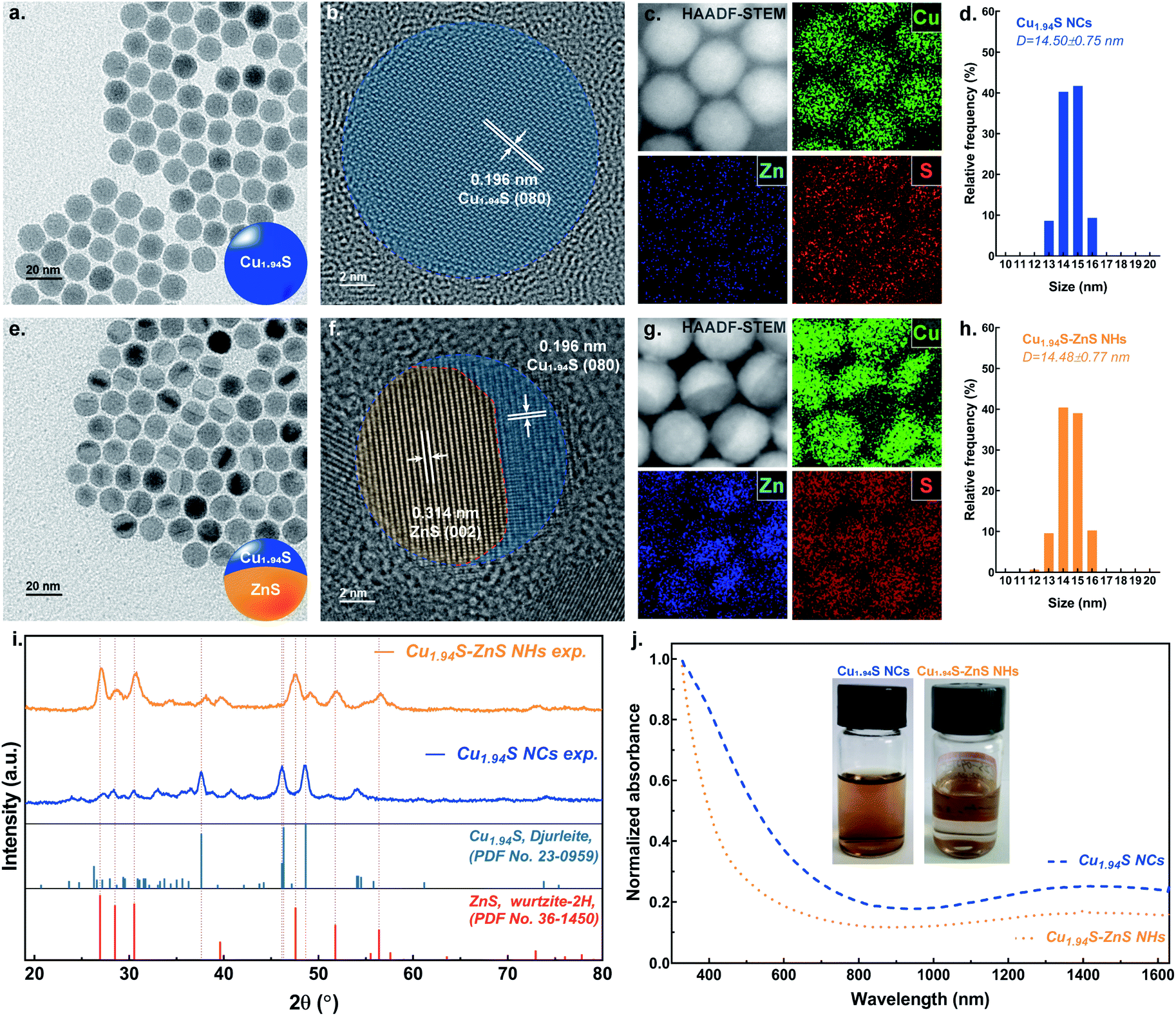 | ||
| Fig. 1 Key characterization data for Cu1.94S NCs and Cu1.94S–ZnS NHs. (a and e) Bright-field TEM images of Cu1.94S NCs and Cu1.94S–ZnS NHs. (b and f) High-resolution TEM images of Cu1.94S NCs and Cu1.94S–ZnS NHs. (c and g) HAADF-STEM images and STEM-EDS elements maps of Cu1.94S NCs and Cu1.94S–ZnS NHs. (d and h) Size distribution histograms of Cu1.94S NCs and Cu1.94S–ZnS NHs. (i) Powder XRD patterns of Cu1.94S NCs and Cu1.94S–ZnS NHs. (j) UV-vis-NIR absorption spectra and digital photographs (inset) of Cu1.94S NCs and Cu1.94S–ZnS NHs dispersed in N-methyl pyrrolidone (NMP). | ||
The TEM image of the nanoparticles after CE is shown in Fig. 1e. Quasi-symmetric bright and dark phases can be observed in a single particle, suggesting the formation of two distinct crystalline phases. The morphology of the resulting particles is still spherical and there is no significant difference in their size distributions before and after CE (Fig. 1h). A relatively low-magnification TEM image that better displays the Cu1.94S–ZnS NHs is shown in Fig. S1.† In contrast to the parent Cu1.94S NCs, an explicit grain boundary can be observed in the particle after CE under HRTEM (Fig. 1f). The lattice spacing of 0.314 nm (3.14 Å) corresponds to the (002) plane of ZnS while the lattice spacing of 0.196 nm (1.96 Å) is still attributed to the (080) plane of Cu1.94S. The HRTEM image also indicates the neat alignment of the parental and heterogeneous atoms located at the interfacial lattice and lattice defects are barely observed, revealing the high-quality interfaces in the Cu1.94S–ZnS NHs (see Fig. S2†). The HAADF-STEM image of the as-synthesized NHs also shows quasi-symmetric bright and dark phases in a single particle (Fig. 1g). When combined with the analysis of STEM-EDS element maps, it appears that the bright phase consists of Cu while the dark phase is composed of Zn. The sulfur element evenly distributes throughout the whole particle. The TEM analysis indicates that the resulting single-particulate NHs retain the overall spherical morphology and size of the parent Cu1.94S NCs with continuous S sublattices and regular interfacial structures. Noteworthily, the obtained Cu1.94S–ZnS NHs is Janus-like (single-tip structure), different from the reported sandwich-like Cu1.8S–ZnS NHs.40 This can be attributed to the lower Zn2+ concentration and higher exchange temperature in our reaction system. Similar exchange patterns have also been observed in the synthesis of Cu1.8S–ZnS heterostructured nanorods when using a low concentration Zn2+ solution at 120 °C.38,39
The structural transformations of the nanoparticles before and after CE were investigated by powder X-ray diffraction (XRD). The XRD pattern (Fig. 1i) of the Cu1.94S NCs is dominated by monoclinic djurleite peaks which correspond to the reflections of bulk djurleite Cu1.94S (pdf no. 23-0959). The characteristic peaks at 37.62°, 46.31° and 48.65° are attributed to the (804), (080) and (1204) planes of djurleite Cu1.94S, respectively. The XRD pattern of the nanoparticles after partial CE evidences the presence of a second majority phase, which can be indexed to hexagonal wurtzite ZnS (pdf no. 36-1450). The peaks at 26.91°, 30.53° and 47.56° correspond to the (100), (101), and (110) planes of wurtzite ZnS, respectively. Previous work has indicated that the lattice structure of parent NCs dominates the crystallographic forms of the final products.32 For example, using roxbyite Cu1,8S NCs as the template results in wurtzite ZnS, while employing digenite Cu1.8S NCs as the parent crystal leads to zincblende ZnS.32 However, in our work, the wurtzite ZnS phase can be also obtained when using djurleite Cu1.94S NCs as the host lattice template. That is because the lattice parameters of djurleite Cu1.94S are similar to those of roxbyite Cu1.8S (see Table S1†). It should be noted that the diffraction peaks of djurleite Cu1.94S slightly shift to higher 2θ after CE, increasing by ∼0.5°. This change can be ascribed to the interfacial strain-induced lattice spacing shrinking when introducing the ZnS to the incipient lattice.31
To calculate the lattice mismatch of Cu1.94S–ZnS NHs, the standard crystalline structure data of djurleite Cu1.94S and wurtzite ZnS were employed. The lattice constants for the S2− sublattice in monoclinic Cu1.94S have average values of a = 3.877 Å and c = 6.716 Å. The lattice constants for the S2− sublattice in hexagonal ZnS are 3.811 Å and 6.234 Å for a and c, respectively. The c/a ratio of Cu1.94S is ∼1.732, which is close to that of ZnS (∼1.636). The values of lattice mismatch in Cu1.94S–ZnS NHs are ∼1.70%, ∼7.17%, and ∼3.39% in the a–a, c–c, and angled (∼40.8°) directions, respectively (see Table S2 and Fig. S3†). This suggests that such small values of lattice mismatch are favorable to the formation of high-quality interfaces with reduced interfacial strain. A previous work has also reported similar lattice mismatch values in Cu1.8S–ZnS heterostructured nanorods synthesized via CE.39
As nanosized ZnS is a wide bandgap semiconductor (Eg = 3.7 eV), its peak absorption is concentrated at ∼340 nm and absorption from 400 nm to the near-infrared region is barely observed, as shown in Fig. S4.†![[thin space (1/6-em)]](https://www.rsc.org/images/entities/char_2009.gif) 41 Meanwhile, due to their narrow bandgap and LSPR effect, the linear absorption range of Cu2−xS NCs is from ultraviolet (UV) to near-infrared (NIR) with a significant attenuation at ∼900 nm.42 When combining the ZnS with LSPR Cu2−xS NCs, in theory, two possible behaviors of linear absorption are expected: the attenuation of absorption in the NIR region and the blueshift of the absorption peak in the short wavelength range. Fig. 1j exhibits the UV-vis-NIR spectra of Cu1.94S NCs and Cu1.94S–ZnS NHs which show linear absorption behaviors accordant to the theoretical expectations. The inset of Fig. 1j shows digital photographs of Cu1.94S NCs and Cu1.94S–ZnS NHs dispersed in N-methyl pyrrolidone (NMP). The color of the suspended solution changes from dark brown to light brown after CE, which is consistent with the results of the UV-vis-NIR spectra and is attributed to the attenuated absorption of visible light.
41 Meanwhile, due to their narrow bandgap and LSPR effect, the linear absorption range of Cu2−xS NCs is from ultraviolet (UV) to near-infrared (NIR) with a significant attenuation at ∼900 nm.42 When combining the ZnS with LSPR Cu2−xS NCs, in theory, two possible behaviors of linear absorption are expected: the attenuation of absorption in the NIR region and the blueshift of the absorption peak in the short wavelength range. Fig. 1j exhibits the UV-vis-NIR spectra of Cu1.94S NCs and Cu1.94S–ZnS NHs which show linear absorption behaviors accordant to the theoretical expectations. The inset of Fig. 1j shows digital photographs of Cu1.94S NCs and Cu1.94S–ZnS NHs dispersed in N-methyl pyrrolidone (NMP). The color of the suspended solution changes from dark brown to light brown after CE, which is consistent with the results of the UV-vis-NIR spectra and is attributed to the attenuated absorption of visible light.
The changes in the chemical states of the elements in the nanoparticles before and after CE were examined by X-ray photoelectron spectroscopy (XPS). Fig. 2 shows the survey spectra and high-resolution spectra of the nanoparticles before and after CE. The peak identifications are summarized in Table S3.† For the samples both before and after CE, distinct peaks can be observed in the XPS spectra of the Cu 2p region. The peaks at ∼932 eV and ∼951 eV correspond to Cu 2p3/2 and 2p1/2, respectively. Copper is present solely in the cuprous state (Cu(I)) in both samples as no Cu(ii) satellite peaks are observed.29 A slight chemical shift (∼0.15 eV) for Cu 2p3/2 was observed after CE (Fig. 2b). This is attributed to a change in interfacial chemical bonds in which partial Cu–S–Cu bonds in Cu1.94S NCs transform into Cu–S–Zn bonds after CE. In the region of Zn 2p, characteristic peaks are only observed in the sample of Cu1.94S–ZnS NHs, suggesting the existence of Zn only after CE. The peaks of Zn 2p3/2 and 2p1/2 located at ∼1021 eV and ∼1044 eV (Fig. 2c), respectively, are consistent with those of Zn(ii).43 In the S 2p region, the peaks at 161.59 eV and 162.74 eV can be assigned to S 2p3/2 and S 2p1/2, respectively. As it is hard to tell the difference between S 2p before and after CE from the original spectra, Gaussian fitting was employed to process the pristine S 2p data (Fig. 2d). Empirically, the binding energy of S 2p3/2 in sulfides with low valency (S2−) is lower than that in sulfur (S0) or sulfides with high valency (S22−), although the valency of S in copper sulfide is still an ongoing debate.29 For example, the binding energies of 2p3/2 in S8 and FeS2 are 164.00 eV and 162.90 eV, respectively.44,45 Thus, it is reasonable to infer that the valency of S in Cu1.94S NCs and Cu1.94S–ZnS NHs is equal to −2. Moreover, the fitting curves indicate that the S 2p3/2 peak at 161.59 eV splits from the middle to both sides after CE. The chemical shift of S 2p3/2 is extremely small (0.2–0.3 eV), suggesting that the valency of S is unchanged. The split peaks of S 2p3/2 around 161.59 eV reveal two different chemical states of the S element (i.e. Cu–S and Zn–S) in Cu1.94S–ZnS NHs.
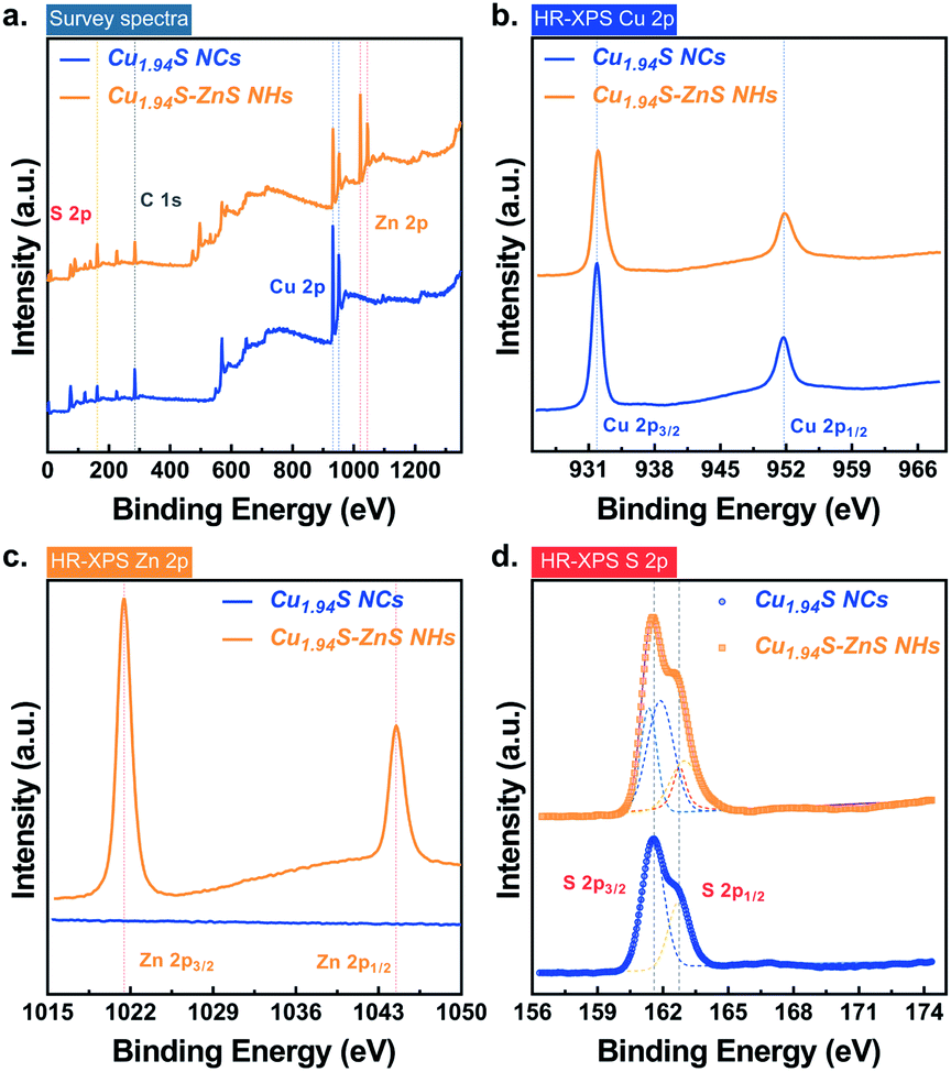 | ||
| Fig. 2 Chemical states of the elements in Cu1.94S NCs and Cu1.94S–ZnS NHs. (a) XPS survey spectra of Cu1.94S NCs and Cu1.94S–ZnS NHs. (b–d) High-resolution XPS spectra (HR-XPS) of Cu 2p, Zn 2p, and S 2p. | ||
2.2 Nonlinear optical (NLO) response of Cu1.94S NCs and Cu1.94S–ZnS NHs
To confirm the existence of plasma-induced charge transfer in the Cu1.94S–ZnS NHs, OA Z-scan experiments were carried out at a wavelength of 1500 nm as this technique has been widely applied for the investigation of energy transfer in hybrid systems.46–48 The samples were spin-coated onto a quartz plate for the measurements. The incident laser beam was focused by a lens with a focal distance of 150 mm. Fig. 3 shows the OA Z-scan results of Cu1.94S NCs and Cu1.94S–ZnS NHs with various excitation intensities. The sharp, narrow peaks show the characteristics of saturable absorption, which is similar to the previous observations in Cu1.8S NCs and Cu2S nanosheets at 1560 nm.49,50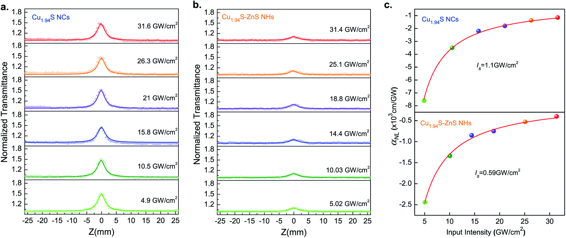 | ||
| Fig. 3 Open-aperture (OA) Z-scan measurements of Cu1.94S NCs (a) and Cu1.94S–ZnS NHs (b) under 1500 nm radiation with different input intensities. Nonlinear optical (NLO) absorption coefficients with various excitation intensities (c). | ||
Given that the excitation energy at 1500 nm (∼0.83 eV) is much lower than the bandgap of Cu1.94S (∼1.51 eV, Fig. S5†), it seems impossible for electrons in the valence band (VB) to be excited directly into the conduction band (CB) and further result in the bleaching effect. However, the intrinsic hole region resulting from the Cu-deficiency can form trap states within the bandgap.51,52 Under irradiation, these trap states bridge electrons jumping from VB to CB by absorbing multi-photons with low energy, which makes the photobleaching effect possible.53 A schematic diagram of the saturable absorption is exhibited in Scheme 1a. In Cu1.94S NCs, with the increase of the laser intensity, the excitation and re-excitation of electrons from lower levels (VB or trap states) to higher energy levels (trap states or CB) are very fast, while the reverse relaxation process is quite slow. Therefore, the key mechanism responsible for the observed phenomenon is the different rates of excitation and relaxation. Only when the excitation rate is faster than the relaxation rate can net electron increase be generated in the excited levels. When the excitation light intensity is strong enough, according to the Pauli blocking principle, all available states in the higher energy level are filled with photo-generated carriers, which prevents further excitation of electrons in the VB, resulting in a photo-bleaching effect.
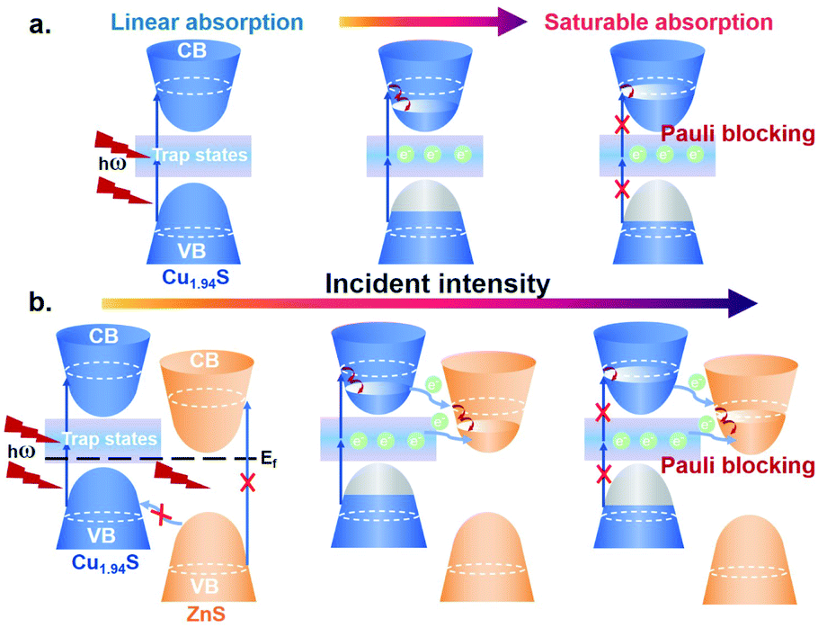 | ||
| Scheme 1 Schematic diagrams of optical saturable absorption in Cu1.94S NCs (a) and Cu1.94S–ZnS NHs (b). CB: conduction band, VB: valence band and Ef: Fermi level. | ||
Although both Cu1.94S NCs and Cu1.94S–ZnS NHs exhibit the characteristic of saturable absorption, the transmittance peak intensity of Cu1.94S NCs is much stronger than that of Cu1.94S–ZnS NHs under the same irradiation intensity, indicating that the photobleaching effect of Cu1.94S–ZnS NHs is weaker than that of Cu1.94S NCs. The lower transmittance intensity of Cu1.94S–ZnS NHs may result from two possible reasons: more photon absorption near the focal point created by charge transfer and reduced content of Cu1.94S in the NHs after CE.
To confirm the above hypothesis, an NLO response experiment was carried out on Cu1.94S–ZnS NHs with lower ZnS content (Cu1.94S–(LZ)ZnS NHs) under the same conditions as outlined above. The Cu1.94S–(LZ)ZnS NHs were synthesized via CE using an exchange solution with a lower Zn2+ concentration. The TEM images of Cu1.94S–ZnS NHs and Cu1.94S–(LZ)ZnS NHs are shown in Fig. S6b.† Theoretically, if the transmittance intensity correlates closely with the content of Cu1.94S, the transmittance intensity of the newly prepared sample should be strong and close to that of pure Cu1.94S NCs. Otherwise, if the absorption behavior is associated with the charge transfer from Cu1.94S to ZnS, the transmittance intensity should remain relatively low, showing a similar pattern to that of Cu1.94S–ZnS NHs. Fig. S6c† presents the OA Z-scan results of pure Cu1.94S NCs, Cu1.94S–ZnS NHs, and Cu1.94S–(LZ)ZnS NHs. It indicates that the charge transfer from Cu1.94S to ZnS is the dominant cause of the weaker saturable absorption behavior of Cu1.94S–ZnS NHs.
For a better understanding of the weaker saturable absorption phenomenon in Cu1.94S–ZnS NHs, a charge transfer mechanism based on the donor–acceptor model is proposed, as shown in Scheme 1b. Copper sulfide (Cu2−xS) is a p-type semiconductor with a Fermi level located near its VB, while zinc sulfide (ZnS) is an n-type semiconductor whose Fermi level lies close to its CB.54,55 In Cu1.94S–ZnS NHs, a p–n heterojunction is formed during the CE. Due to the existence of the internal electrostatic field in the p–n junction region, the equilibrium of Fermi energy in the NHs makes the CB of Cu1.94S locate above the CB of ZnS. Due to the existence of the ZnS phase in Cu1.94S–ZnS NHs, more orbitals in the CB that can be occupied by photo-generated carriers are provided. Electrons in the VB of ZnS are unable to be directly excited by low energy incident light (i.e. NIR); as a result, the CB of ZnS is unfilled. Therefore, the excited electrons in the higher energy level CB of Cu1.94S can easily transfer to the CB of ZnS, leading to more absorption of incident photons and weaker saturable absorption. It should be noted that the electron transfer route from the trap states of Cu1.94S to the CB of ZnS cannot be excluded as the energy level is unclear. In addition, electrons in the VB of ZnS are unable to be transferred to the VB of Cu1.94S under NIR irradiation because the energy barrier is larger than the incident light energy.56
To quantitatively evaluate the NLO absorption coefficients and saturable intensity of the samples, the normalized OA Z-scan data were fitted using the following equations57–59
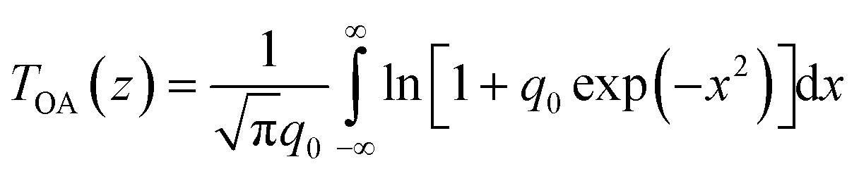 | (1) |
| αNL(I) = α0NL/(1 + I/IS) | (2) |
The NLO absorption coefficients of Cu1.94S NCs and Cu1.94S–ZnS NHs were extracted by fitting eqn (1) to the experimental OA Z-scan data. As shown in Fig. 3c, the solid curves represent the fitting results based on the NLO absorption model, which agrees well with the experimental data. For Cu1.94S NCs, the NLO absorption coefficient αNL increases from −7.6 × 103 cm GW−1 to −1.15 × 103 cm GW−1 when the excitation intensity increases from 4.9 GW cm−2 to 31.6 GW cm−2. It was found that the αNL initially increases rapidly and then gradually stabilizes as the excitation intensity continues to increase. A similar trend is also observed in the Cu1.94S–ZnS NHs. The Is values of Cu1.94S NCs and Cu1.94S–ZnS NHs are 1.1 GW cm−2 and 0.59 GW cm−2, respectively. Moreover, the peak intensity only slightly changes with increasing incident intensity, suggesting that the NLO absorption is insensitive to the excitation intensity. Similar saturable absorption phenomena were observed in previously reported Bi2TexSe3−x nanosheets.60 Our results indicate that the Cu1.94S–ZnS NHs possess a fascinating NLO response in the NIR band.
2.3 Carrier dynamics of Cu1.94S NCs and Cu1.94S–ZnS NHs
As mentioned in recent literature, the interfacial structure is one of the essential factors that dominate interdomain charge communications in NHs.17,61 It is worth exploring the carrier dynamics in the as-synthesized Cu1.94S–ZnS NHs on account of their neat interfacial structures, as the existence of charge transfer was confirmed by the OA Z-scan experiments. To investigate the plasmon-induced carrier dynamics in Cu1.94S–ZnS NHs, femtosecond time-resolved pump–probe experiments were carried out at a wavelength of 1500 nm, which is in the LSPR-induced NIR absorption region of Cu1.94S NCs. The average power of the pump light was from 0.3–0.6 μW, which is below the excitation intensity of the NMP solvent. The excitation intensity of the probe light was less than 10% that of the pump light. To reduce the experimental uncertainty of pump–probe measurements, the light path was well-calibrated with a standard sample before testing (see Fig. S7†).Once the pump beam is injected into the sample, a carrier relaxation process can be observed after the initial response. Fig. 4a and b depict the transient transmission intensity as a function of the delay time for the samples at different excitation intensities. All the transient signals clearly show exponential decay. A biexponential decay model, y = A1exp(−t/τ1) + A2exp(−t/τ2), is employed to fit these recorded signals. For Cu1.94S NCs, two identical delay times are obtained from the fitted pump–probe data, approximately 0.46–0.53 ps (average 0.50 ± 0.03 ps) at different excitation intensities, indicating that only one decay process is observed in Cu1.94S NCs (Fig. 4a). This process can be assigned to the intra-band relaxation of the hot electrons according to previous reports.52,62Fig. 4b presents the carrier dynamics relaxation process for the Cu1.94S–ZnS NHs. The average values of τ1 and τ2 are 0.091 ± 0.010 ps and 1.01 ± 0.05 ps, respectively. Fig. 4c demonstrates the carrier relaxation time as a function of the input power, indicating that the carrier relaxation time is independent of the excitation intensity. Compared to Cu1.94S NCs, two distinct relaxation processes were observed in the Cu1.94S–ZnS NHs. In line with that of the standard sample (see Fig. S8†), the relaxation time of 1.01 ± 0.05 ps (τ2) can be ascribed to the intra-band relaxation process of ZnS. The relaxation time of 0.091 ± 0.010 ps (τ1) corresponds to the charge transfer process in Cu1.94S–ZnS NHs according to the donor–acceptor model proposed in the Z-scan. Upon NIR irradiation, electrons in the VB are excited into a higher energy level (trap states or CB) of Cu1.94S and the photo-induced electrons in the excited states of Cu1.94S can intensively inject into the lower CB of ZnS. Subsequently, the photoexcited electrons in the CB of ZnS relax to the bottom of the CB through electron–electron scattering. Therefore, the ultrafast relaxation time of τ1 can be attributed to plasmon-induced hot electron transfer from Cu1.94S to ZnS. However, it is difficult to distinguish the transfer routes (CB → CB or trap states → CB) and we can only determine that the charge transfer time from Cu1.94S to ZnS is ∼0.091 ps. To avoid mixing up the intra-band relaxation kinetics with the charge transfer component, we tried to fit the ratio curve of Cu1.94S–ZnS to Cu1.94S.70,71 However, as the signal intensities of Cu1.94S NCs and Cu1.94S–ZnS NHs are very close and given the existence of laser noise, it is difficult to analyze the ratio curve of Cu1.94S–ZnS to Cu1.94S to obtain the charge transfer dynamics characteristics.
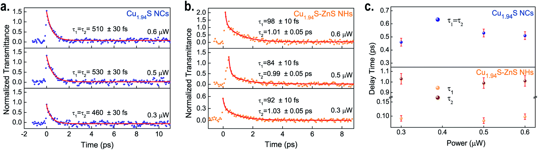 | ||
| Fig. 4 Pump–probe signals at 1500 nm under different excitation intensities for Cu1.94S NCs (a) and Cu1.94S–ZnS NHs (b). Photoexcited carrier relaxation time as a function of the input energy (c). | ||
Table 1 summarizes the carrier transfer times in different NHs synthesized via CE and traditional epitaxial growth, including metal–semiconductor hybrid NCs and semiconductor–semiconductor NHs. It reveals that the PICT time of the as-synthesized Cu1.94S–ZnS NHs is faster than those of conventional NHs, suggesting an ultrafast PICT response in Cu1.94S–ZnS NHs under NIR irradiation. This ultrafast PICT process is attributed to the well-ordered interfacial structure in the Cu1.94S–ZnS NHs synthesized by CE. Because of the continuous anion sublattice, the dangling bonds are saturated and the lattice mismatch between the heterogeneous crystalline phases is relatively small (1.7%), resulting in decreased interfacial strain and fewer defects.39,63,64 These help to reduce the recombination centers at the interfaces and facilitate charge communications among the domains of the particles. Our results indicate that the Cu1.94S–ZnS NHs possess an excellent NLO response in the NIR band, revealing their great potential for applications in ultrafast photonics and biomedicine.65–67
| Wavelength (nm) | Samples | Synthesis methodsa | Shapes | τ CT (ps) | Ref. | |
|---|---|---|---|---|---|---|
| Pump | Probe | |||||
| a CE: cation exchange reaction, CVD: chemical vapor deposition, SG: seed-mediated growth. | ||||||
| 1500 | 1500 | Cu1.94S–ZnS | CE | Particles (Janus) | ∼0.091 | This work |
| 550 | 3500 | Au–TiO2 | Annealing | Film | ∼0.240 | 4 |
| 400 | 650 | Au–MoS2 | Template CVD | Film | ∼0.200 | 5 |
| 400 | 532 | Ag–graphene | CVD/wet transfer | Nanowires/film | ∼0.500 | 68 |
| 420 | 420 | ZnSe–CdS–ZnSe | SG | Rods (Barbell) | ∼0.350 | 64 |
| 400 | 500 | ZnTe–CdSe | SG | Particles (core–shell) | ∼0.670 | 69 |
| 470 | 470 | CdZnS–ZnSe | SG | Particles (core–shell) | ∼50.000 | 7 |
As the Cu1.94S–ZnS NHs possess remarkable saturable absorption properties and exhibit a fascinating dynamic response, we anticipate that the Cu1.94S–ZnS NHs may have potential for significant applications in pulse lasers and optical switching. The obtained NLO absorption coefficient of Cu1.94S–ZnS NHs at 1500 nm is very close to that of TiS2, indicating that the Cu1.94S–ZnS NHs may possess wider application prospects in advanced devices like other emerging types of nonlinear optical materials, such as MOF, MXene, graphdiyne, and antimonene.72–75 Therefore, it is necessary to study the NLO response characteristics of Cu1.94S–ZnS NHs at various wavelengths and its application in mode-locking in subsequent works to promote its further development for a wider range of applications in photonics devices such as sensors, optical information converters, and detectors.76–78
3. Conclusions
In summary, the femtosecond OA Z-scan measurements and femtosecond time-resolved pump–probe technique were employed to investigate plasmon-induced charge transfer in single-particulate Cu1.94S–ZnS NHs. Our experimental data provide assertive evidence for plasmon-induced charge transfer between the Cu1.94S and ZnS domains in the single-particulate Cu1.94S–ZnS NHs. The unique interfacial structures of Cu1.94S–ZnS NHs lead to ultrafast electron injection (τCT = 0.091 ± 0.01 ps) from Cu1.94S to ZnS, which, to our knowledge, is rarely observed in semiconductor–semiconductor NHs. These findings suggest that constructing neat interfacial structures is one of the most important approaches to improving the utilization of photons. Our results can be also referenced to understand how to design the interface to control hot electron injection. Moreover, in addition to creating high-ordered complex nanoheterostructures and metastable crystalline structures, CE can be also used as an efficient method to build fine interfacial structures in nanocrystals, which is significant for engineering plasmon-induced charge transfer-based materials and devices with high efficiency.4. Experimental section
4.1 Materials
Cupric(II) acetylacetonate (Cu(acac)2, 97%), octadecene (ODE, 90%) and 1-dodecanethiol (1-DDT, 98%) were purchased from Aladdin (China). High-purity oleylamine (OLAM, 97%) was purchased from Sigma Aldrich (United States). Zinc chloride (ZnCl2, 98%) and trioctylphosphine (TOP, 90%) were from Macklin (China). Other analytical grade solvents, including ethanol, N-methyl pyrrolidone (NMP) and hexanes, were purchased from Sinopharm (China). All reagents were used as received without further purification.4.2 Synthesis of djurleite Cu1.94S NCs
Spherical Cu1.94S NCs were synthesized by a high-temperature thermal decomposition method. Typically, at room temperature, 4.00 mmol of Cu(acac)2 and 60.00 mmol of 1-DDT were loaded in a 100 mL 3-neck round-bottom flask equipped with a condenser, thermocouple, gas flow adapter, and magnetic stir bar. This mixture was gently stirred for 10 minutes and placed under a blanket of Ar after cycling with vacuum and Ar three times. Under the protection of the Ar blanket, the flask was placed into a pre-heated oil-bath. The reaction temperature was increased to 205 °C within 5 minutes. During the heating period, the mixture changed from milky white to transparent light yellow, indicating the formation of the Cu–thiol complex. Upon reaching 205 °C, the solution changed from transparent light yellow to dark brown over ∼4 minutes, revealing the beginning of nucleation in the reaction system. The reaction was allowed to proceed at this temperature for 120 minutes before being cooled rapidly by an ice water bath and the resulting mixture was turbid brown. The product was precipitated by adding 40 mL of ethanol and isolated by centrifugation at 8000 rpm for 10 minutes. The obtained Cu1.94S NCs were redispersed in 10 mL of hexane, and the precipitation/isolation process was repeated three times. Finally, the nanoparticles were dispersed in 10 mL of hexane or dried in a vacuum for storage and further use.4.3 Synthesis of Cu1.94S–ZnS NHs via cation exchange reaction
Cu1.94S–ZnS NHs were synthesized using a stoichiometrically limited cation exchange reaction as described in a previous report with slight modifications.38,39 The exchange solution was prepared by dissolving 0.25 mmol of ZnCl2 in 24.00 mmol of OLAM and 30.00 mmol of ODE. Then, the exchange solution was heated to 180 °C under an Ar blanket and allowed to react for 30 minutes to form a homogeneous Zn-OLAM precursor before cooling to the exchange temperature (∼105 °C). In a separate glass vial, 0.50 mmol of Cu1.94S NCs was mixed with 4.00 mmol of TOP and 15.63 mmol of ODE. The mixture was sealed in the glass vial under Ar protection and sonicated at room temperature for 10 minutes to form a colloidal suspension. The Cu1.94S NCs suspension was swiftly injected into the exchange solution at 105 °C and the cation exchange reaction was allowed to proceed for 15 minutes before being quenched by the ice water bath. The precipitation/centrifugation procedure was as described above. The resulting Cu1.94S–ZnS NHs were dried and stored under the vacuum. The dried Cu1.94S–ZnS NHs powder was suspended in hexane or NMP for characterization and further use. The synthesis procedure of Cu1.94S–(LZ)ZnS NHs was similar to that outlined above except that the dose of ZnCl2 was decreased to 0.12 mmol.4.4 Nonlinear optical (NLO) response and carrier dynamics measurements
Femtosecond open-aperture (OA) Z-scan measurements and the femtosecond time-resolved pump–probe technique were employed to investigate the NLO response and the photoexcited carrier dynamics of the samples, respectively. The laser pulse was delivered by an optical parametric amplifier (TOPAS, USF-UV2), pumped by a Ti:sapphire regenerative amplifier system (Spectra-Physics, Spitfire ACE-35F-2KXP, Maitai SP and Empower 30) with a pulse duration of 35 fs and repetition rate of 2 kHz. The focal distance of the lens is 150 mm and the minimum beam waist was approximately 38 mm. The samples were spin-coated onto quartz plates for Z-scan measurements and dispersed in NMP for the pump–probe tests. The experimental setups are shown in Scheme S1.†4.5 Characterizations
Transmission electron microscopy (TEM) and high-resolution TEM (HRTEM) images were collected on an FEI Titan G2 60-300 TEM operating at 300 kV. High angle annular dark-field scanning TEM (HAADF-STEM) images and STEM energy-dispersive spectroscopy (STEM-EDS) maps were collected on an FEI Talos F200X S/TEM at an accelerating voltage of 200 kV. All the samples for TEM analysis were drop-cast from a nanoparticle/hexane suspension onto 400-mesh molybdenum (Mo) grids with carbon/formvar film. Before the TEM measurements, all samples were treated with a plasma cleaner. A Bruker D8 Advance X-ray diffractometer using Cu Kα radiation (λ = 0.15418 nm) was employed to record the powder X-ray diffraction patterns of the samples. The chemical compositions of the samples were analyzed on a Thermo Scientific ESCALAB Xi X-ray photoelectron spectrometer (XPS). The absorption spectra of the samples from the ultraviolet (UV) to near-infrared (NIR) region were recorded on a Hitachi U-4100 UV-vis-NIR spectrophotometer.Author contributions
WW, XG and YL conceived the project; SL and WW synthesized the nanoparticles; SL, WW, YY, CL and QT performed the TEM, XRD, XPS, and UV-vis-NIR characterizations; SL and WW carried out the pump–probe and OA Z-scan measurements. The manuscript was written by WW and SL, and the manuscript was revised by XG, WW, YY and YL. All authors have approved the final version of the manuscript.Conflicts of interest
There are no conflicts to declare.Acknowledgements
The authors would like to thank Prof. Si Xiao, Prof. Jun He, and Dr Yingwei Wang from the school of physics and electronics of Central South University for their kind discussion. The authors acknowledge the funding support from the Hainan Department of Science and Technology of China (grant number: ZDYF2018104), National Natural Science Foundation of China (grant number: 81760138, 61774169), and Qingyuan Innovation and Entrepreneurship Research Team Project (grant number: 2018001).Notes and references
- D. C. Ratchford, ACS Nano, 2019, 13, 13610–13614 CrossRef CAS PubMed.
- M. L. Brongersma, N. J. Halas and P. Nordlander, Nat. Nanotechnol., 2015, 10, 25–34 CrossRef CAS PubMed.
- C. F. Bohren, Am. J. Phys., 1983, 51, 323–327 CrossRef CAS.
- A. Furube, L. Du, K. Hara, R. Katoh and M. Tachiya, J. Am. Chem. Soc., 2007, 129, 14852–14853 CrossRef CAS PubMed.
- Y. Yu, Z. Ji, S. Zu, B. Du, Y. Kang, Z. Li, Z. Zhou, K. Shi and Z. Fang, Adv. Funct. Mater., 2016, 26, 6394–6401 CrossRef CAS.
- K. Wu, J. Chen, J. R. McBride and T. Lian, Science, 2015, 349, 632–635 CrossRef CAS PubMed.
- L. Ran, H. Li, W. Wu, Y. Gao, Z. Chai, J. Xiao, Q. Li and D. Kong, Opt. Express, 2018, 26, 18480 CrossRef CAS PubMed.
- J. Ma and S. Gao, ACS Nano, 2019, 13, 13658–13667 CrossRef CAS PubMed.
- J. Yu, J. Zhang and S. Liu, J. Phys. Chem. C, 2010, 114, 13642–13649 CrossRef CAS.
- U. T. D. Thuy, N. Q. Liem, C. M. A. Parlett, G. M. Lalev and K. Wilson, Catal. Commun., 2014, 44, 62–67 CrossRef CAS.
- Y. Hong, J. Zhang, F. Huang, J. Zhang, X. Wang, Z. Wu, Z. Lin and J. Yu, J. Mater. Chem. A, 2015, 3, 13913–13919 RSC.
- S. Linic, P. Christopher and D. B. Ingram, Nat. Mater., 2011, 10, 911–921 CrossRef CAS PubMed.
- P. Zhang, T. Wang and J. Gong, Adv. Mater., 2015, 27, 5328–5342 CrossRef CAS PubMed.
- R. Shi, Y. Cao, Y. Bao, Y. Zhao, G. I. N. Waterhouse, Z. Fang, L. Z. Wu, C. H. Tung, Y. Yin and T. Zhang, Adv. Mater., 2017, 29, 1700803 CrossRef PubMed.
- J. Zhang, Y. Tang, K. Lee and M. Ouyang, Science, 2010, 327, 1634–1638 CrossRef CAS PubMed.
- T. Sasaki, K. Arafune, W. Metzger, M. J. Romero, K. Jones, M. Al-Jassim, Y. Ohshita and M. Yamaguchi, Sol. Energy Mater. Sol. Cells, 2009, 93, 936–940 CrossRef CAS.
- J. Liu and J. Zhang, Chem. Rev., 2020, 120, 2123–2170 CrossRef CAS PubMed.
- G. Cho, Y. Park, Y.-K. Hong and D.-H. Ha, Nano Convergence, 2019, 6, 17 CrossRef PubMed.
- L. De Trizio and L. Manna, Chem. Rev., 2016, 116, 10852–10887 CrossRef CAS PubMed.
- J. B. Rivest and P. K. Jain, Chem. Soc. Rev., 2013, 42, 89–96 RSC.
- D. H. Son, S. M. Hughes, Y. Yin and A. P. Alivisatos, Science, 2004, 306, 1009–1012 CrossRef CAS PubMed.
- J. Park, H. Zheng, Y. Jun and A. P. Alivisatos, J. Am. Chem. Soc., 2009, 131, 13943–13945 CrossRef CAS PubMed.
- P. K. Jain, L. Amirav, S. Aloni and A. P. Alivisatos, J. Am. Chem. Soc., 2010, 132, 9997–9999 CrossRef CAS PubMed.
- B. J. Beberwyck, Y. Surendranath and A. P. Alivisatos, J. Phys. Chem. C, 2013, 117, 19759–19770 CrossRef CAS.
- G. Gariano, V. Lesnyak, R. Brescia, G. Bertoni, Z. Dang, R. Gaspari, L. De Trizio and L. Manna, J. Am. Chem. Soc., 2017, 139, 9583–9590 CrossRef CAS PubMed.
- R. Tu, Y. Xie, G. Bertoni, A. Lak, R. Gaspari, A. Rapallo, A. Cavalli, L. De Trizio and L. Manna, J. Am. Chem. Soc., 2016, 138, 7082–7090 CrossRef CAS PubMed.
- K. Miszta, G. Gariano, R. Brescia, S. Marras, F. De Donato, S. Ghosh, L. De Trizio and L. Manna, J. Am. Chem. Soc., 2015, 137, 12195–12198 CrossRef CAS PubMed.
- X. Wang, X. Liu, D. Zhu and M. T. Swihart, Nanoscale, 2014, 6, 8852–8857 RSC.
- Y. Liu, M. Liu, D. Yin, W. Wei, P. N. Prasad and M. T. Swihart, Chem. Mater., 2017, 29, 3555–3562 CrossRef CAS.
- A. Nelson, S. Honrao, R. G. Hennig and R. D. Robinson, Chem. Mater., 2019, 31, 991–1005 CrossRef CAS.
- D. H. Ha, A. H. Caldwell, M. J. Ward, S. Honrao, K. Mathew, R. Hovden, M. K. A. Koker, D. A. Muller, R. G. Hennig and R. D. Robinson, Nano Lett., 2014, 14, 7090–7099 CrossRef CAS PubMed.
- J. L. Fenton, B. C. Steimle and R. E. Schaak, Inorg. Chem., 2019, 58, 672–678 CrossRef CAS PubMed.
- J. L. Fenton, B. C. Steimle and R. E. Schaak, J. Am. Chem. Soc., 2018, 140, 6771–6775 CrossRef CAS PubMed.
- J. L. Fenton and R. E. Schaak, Angew. Chem., Int. Ed., 2017, 56, 6464–6467 CrossRef CAS PubMed.
- A. E. Powell, J. M. Hodges and R. E. Schaak, J. Am. Chem. Soc., 2016, 138, 471–474 CrossRef CAS PubMed.
- J. M. Hodges, K. Kletetschka, J. L. Fenton, C. G. Read and R. E. Schaak, Angew. Chem., Int. Ed., 2015, 54, 8669–8672 CrossRef CAS PubMed.
- T. Holtus, L. Helmbrecht, H. C. Hendrikse, I. Baglai, S. Meuret, G. W. P. Adhyaksa, E. C. Garnett and W. L. Noorduin, Nat. Chem., 2018, 10, 740–745 CrossRef CAS PubMed.
- B. C. Steimle, A. M. Fagan, A. G. Butterfield, R. W. Lord, C. R. McCormick, G. A. Di Domizio and R. E. Schaak, Chem. Mater., 2020, 32, 5461–5482 CrossRef CAS.
- B. C. Steimle, J. L. Fenton and R. E. Schaak, Science, 2020, 367, 418–424 CrossRef CAS PubMed.
- J. L. Fenton, B. C. Steimle and R. E. Schaak, Science, 2018, 360, 513–517 CrossRef CAS PubMed.
- N. Prasad and B. Karthikeyan, J. Appl. Phys., 2019, 125, 085702 CrossRef.
- Y. Zhao, H. Pan, Y. Lou, X. Qiu, J. Zhu and C. Burda, J. Am. Chem. Soc., 2009, 131, 4253–4261 CrossRef CAS PubMed.
- B. STROHMEIER, J. Catal., 1984, 86, 266–279 CrossRef CAS.
- S. Karthe, R. Szargan and E. Suoninen, Appl. Surf. Sci., 1993, 72, 157–170 CrossRef CAS.
- A. M. de Jong, H. J. Borg, L. J. van IJzendoorn, V. G. F. M. Soudant, V. H. J. de Beer, J. A. R. van Veen and J. W. Niemantsverdriet, J. Phys. Chem., 1993, 97, 6477–6483 CrossRef CAS.
- S.-J. Ding, F. Nan, D.-J. Yang, X.-L. Liu, Y.-L. Wang, L. Zhou, Z.-H. Hao and Q.-Q. Wang, Sci. Rep., 2015, 5, 9735 CrossRef CAS PubMed.
- Y. Wang, H. Mu, X. Li, J. Yuan, J. Chen, S. Xiao, Q. Bao, Y. Gao and J. He, Appl. Phys. Lett., 2016, 108, 221901 CrossRef.
- J.-C. Lan, J. Qiao, W.-H. Sung, C.-H. Chen, R.-H. Jhang, S.-H. Lin, L.-R. Ng, G. Liang, M.-Y. Wu, L.-W. Tu, C.-M. Cheng, H. Liu and C.-K. Lee, Nanoscale, 2020, 12, 16956–16966 RSC.
- Z. Hui, W. Xu, X. Li, P. Guo, Y. Zhang and J. Liu, Nanoscale, 2019, 11, 6045–6051 RSC.
- M. Liu, D. Zhou, Z. Jia, Z. Li, N. Li, S. Li, Z. Kang, J. Yi, C. Zhao, G. Qin, H. Song and W. Qin, J. Mater. Chem. C, 2017, 5, 4034–4039 RSC.
- J. Ludwig, L. An, B. Pattengale, Q. Kong, X. Zhang, P. Xi and J. Huang, J. Phys. Chem. Lett., 2015, 6, 2671–2675 CrossRef CAS PubMed.
- Y. Lou, X. Chen, A. C. Samia and C. Burda, J. Phys. Chem. B, 2003, 107, 12431–12437 CrossRef CAS.
- R. F. Zhang, D. Z. Guo and G. M. Zhang, Appl. Surf. Sci., 2017, 426, 763–769 CrossRef CAS.
- K. S. Ranjith, D. Ranjith Kumar, Y. S. Huh, Y.-K. Han, T. Uyar and R. T. Rajendra Kumar, J. Phys. Chem. C, 2020, 124, 3610–3620 CrossRef CAS.
- C. Mondal, A. Singh, R. Sahoo, A. K. Sasmal, Y. Negishi and T. Pal, New J. Chem., 2015, 39, 5628–5635 RSC.
- I. K. Vereshchagin, Russ. Phys. J., 1998, 41, 171–173 CrossRef CAS.
- Y. Wang, Y. Wang, K. Chen, K. Qi, T. Xue, H. Zhang, J. He and S. Xiao, ACS Nano, 2020, 14, 10492–10502 CrossRef CAS PubMed.
- Y. Wang, H. Mu, X. Li, J. Yuan, J. Chen, S. Xiao, Q. Bao, Y. Gao and J. He, Appl. Phys. Lett., 2016, 108, 221901 CrossRef.
- Y. W. Wang, S. Liu, B. W. Zeng, H. Huang, J. Xiao, J. B. Li, M. Q. Long, S. Xiao, X. F. Yu, Y. L. Gao and J. He, Nanoscale, 2017, 9, 4683–4690 RSC.
- Y. Wang, S. Liu, J. Yuan, P. Wang, J. Chen, J. Li, S. Xiao, Q. Bao, Y. Gao and J. He, Sci. Rep., 2016, 6, 33070 CrossRef CAS PubMed.
- E. Khon, A. Mereshchenko, A. N. Tarnovsky, K. Acharya, A. Klinkova, N. N. Hewa-Kasakarage, I. Nemitz and M. Zamkov, Nano Lett., 2011, 11, 1792–1799 CrossRef CAS PubMed.
- Y. Lou, C. Burda, M. Yin and S. O'Brien, in Physical Chemistry of Interfaces and Nanomaterials III, ed. G. V. Hartland and X.-Y. Zhu, 2004, vol. 5513, p. 30 Search PubMed.
- M. Liu, Y. Liu, B. Gu, X. Wei, G. Xu, X. Wang, M. T. Swihart and K. T. Yong, Chem. Soc. Rev., 2019, 48, 4950–4965 RSC.
- N. N. Hewa-Kasakarage, P. Z. El-Khoury, A. N. Tarnovsky, M. Kirsanova, I. Nemitz, A. Nemchinov and M. Zamkov, ACS Nano, 2010, 4, 1837–1844 CrossRef CAS PubMed.
- Y. Wang, K. Chen, H. Hao, G. Yu, B. Zeng, H. Wang, F. Zhang, L. Wu, J. Li, S. Xiao, J. He, Y. Zhang and H. Zhang, Nanoscale, 2019, 11, 2637–2643 RSC.
- J. Liu, Y. Chen, Y. Li, H. Zhang, S. Zheng and S. Xu, Photonics Res., 2018, 6, 198 CrossRef CAS.
- H. Zhang, S. B. Lu, J. Zheng, J. Du, S. C. Wen, D. Y. Tang and K. P. Loh, Opt. Express, 2014, 22, 7249 CrossRef CAS PubMed.
- Q. Ding, Y. Shi, M. Chen, H. Li, X. Yang, Y. Qu, W. Liang and M. Sun, Sci. Rep., 2016, 6, 1–10 CrossRef PubMed.
- S. Jin, J. Zhang, R. D. Schaller, T. Rajh and G. P. Wiederrecht, J. Phys. Chem. Lett., 2012, 3, 2052–2058 CrossRef CAS.
- K. Mishra, A. Das and S. Ghosh, J. Phys. Chem. C, 2020, 124, 24115–24125 CrossRef CAS.
- D. D. Eads, B. G. Dismer and G. R. Fleming, J. Chem. Phys., 1990, 93, 1136–1148 CrossRef CAS.
- Y. Ge, Z. Zhu, Y. Xu, Y. Chen, S. Chen, Z. Liang, Y. Song, Y. Zou, H. Zeng, S. Xu, H. Zhang and D. Fan, Adv. Opt. Mater., 2018, 6, 1701166 CrossRef.
- X. Jiang, A. V. Kuklin, A. Baev, Y. Ge, H. Ågren, H. Zhang and P. N. Prasad, Phys. Rep., 2020, 848, 1–58 CrossRef CAS.
- X. Jiang, L. Zhang, S. Liu, Y. Zhang, Z. He, W. Li, F. Zhang, Y. Shi, L. Wei, Y. Li, Q. Wen, J. Li, J. Feng, S. Ruan, Y. J. Zeng, X. Zhu, Y. Lu and H. Zhang, Adv. Opt. Mater., 2018, 6, 1–11 Search PubMed.
- X. Jiang, A. V. Kuklin, A. Baev, Y. Ge, H. Ågren, H. Zhang and P. N. Prasad, Phys. Rep., 2020, 848, 1–58 CrossRef CAS.
- L. Lu, Z. Liang, L. Wu, Y. Chen, Y. Song, S. C. Dhanabalan, J. S. Ponraj, B. Dong, Y. Xiang, F. Xing, D. Fan and H. Zhang, Laser Photon. Rev., 2018, 12, 1700221 CrossRef.
- L. Wu, Y. Dong, J. Zhao, D. Ma, W. Huang, Y. Zhang, Y. Wang, X. Jiang, Y. Xiang, J. Li, Y. Feng, J. Xu and H. Zhang, Adv. Mater., 2019, 31, 1807981 CrossRef PubMed.
- X. Jiang, S. Liu, W. Liang, S. Luo, Z. He, Y. Ge, H. Wang, R. Cao, F. Zhang, Q. Wen, J. Li, Q. Bao, D. Fan and H. Zhang, Laser Photon. Rev., 2018, 12, 1700229 CrossRef.
Footnote |
| † Electronic supplementary information (ESI) available: Experimental setups, enlarged HRTEM images of the interfacial regions, merged image of Cu1.94S–ZnS NHs, TEM image of Cu1.94S–(LZ)ZnS NHs, idealized projections of the crystal planes of sulfur sublattice in ZnS and Cu1.94S, simulated XRD patterns, pump–probe results for standard sample and solvent, relevant calculation parameters, and XPS peak identifications. See DOI: 10.1039/d1na00037c |
| This journal is © The Royal Society of Chemistry 2021 |