
 Open Access Article
 This Open Access Article is licensed under a Creative Commons Attribution-Non Commercial 3.0 Unported Licence
A nanoscale vacuum field emission gated diode with an umbrella cathode
Jin-Woo
Han
 *,
Myeong-Lok
Seol
and
M.
Meyyappan
*,
Myeong-Lok
Seol
and
M.
Meyyappan
NASA Ames Research Center, Moffett Field, CA 94035, USA. E-mail: jin-woo.han@nasa.gov
First published on 1st February 2021
Abstract
A nanoscale field emission vacuum channel gated diode structure is proposed and a tungsten cathode with an umbrella-like geometry and sharp vertical edge is fabricated. The edge of the suspended cathode becomes the field emission surface. Unlike in the traditional transistor with the gate typically located between the source and the drain, the bottom silicon plate becomes the gate here and the anode terminal is located between the umbrella cathode and the gate. The fabricated devices show excellent diode characteristics and the gated diode structure is attractive for extremely low gate leakage.
Introduction
Vacuum electronic devices have a broad set of applications including traveling wave tubes, klystrons, X-ray generators, free electron lasers, field emission displays, radio frequency power sources, miniaturized mass spectrometers, vacuum gauges, and charge neutralizers. The devices in most of these applications are made by machining and not amenable for miniaturization. In addition, the operation voltage is 100s of volts and cannot be scaled down due to their large size. Recently efforts have been made to aggressively miniaturize vacuum electronic devices at the nanoscale with the aid of conventional integrated circuit manufacturing practice.1–5 The nanoscale vacuum field emission transistors (VFETs) have been used for the construction of circuit elements including inverters6 and adders7 for various applications, and even complementary device operation has been proposed for the first time in vacuum electronics to enable low power logic circuits.8 There have been a large number of studies4,9–13 focusing on vacuum diodes with nanoscale gaps as these are easier to fabricate and provide a preliminary understanding of the emission characteristics prior to undertaking complex VFET fabrication. Besides having their own applications, vacuum diodes can be used to optimize several important design, operation and reliability criteria such as channel gaps vs. anode current, impact of material quality on field emission, emission uniformity over the cathode area and many other factors with minimal fabrication efforts. For example, Liu et al. systematically studied the impact of the anode–cathode gap on anode current in the range of 10 to 200 nm for three cathode materials of SiC, VO2 (A) and Cu.9–11 Their study showed an exponential increase in current as the gap is decreased without showing any signs of current saturation even down to 10 nm; this information is valuable in the design of more complex VFETs.In this work, a gated diode structure with a 100 nm anode–cathode gap is experimentally demonstrated. The device features an inverse vertical channel with two major distinctions. First, an innovative fabrication approach makes the cathode have an umbrella-like shape with a sharp-edged rim. Inherent deposition and etching process steps alone allow producing the sharp cathode without any additional dedicated processes to sharpen the corner. Second, the gate is separated from the source (or the cathode) farther than the drain (or the anode), which results in great reduction of the gate leakage. The fabrication details and the measured device characteristics are provided and complemented by multi-physics simulations to gain insight.
Device fabrication
Fig. 1a shows the process steps for the fabrication of an umbrella type inverted vertical field emission gated diode (VFEGD). A 150 mm p-type silicon wafer was used as the starting material. The phosphorous was heavily doped (Nd = 1 × 1020 cm−3) on the wafer and this wafer surface becomes the gate. Silicon nitride (SiN) and in situ doped n+ polySi films were subsequently deposited, followed by patterning (step i in Fig. 1a). The n+ polySi is the anode and the SiN layer is the spacer between the gate and the anode. Silicon dioxide (SiO2) and tungsten (W) were blanket deposited subsequently (step ii). Tungsten is the cathode and SiO2 is in part the spacer between the cathode and the anode, and in part the sacrificial layer to create the vacuum channel. At this point, the conformal film deposition makes the downward curved W over the n+ polySi corner. Then, the top electrode W was patterned over the rounded region (step iii) and as a result, the downward edge became sharp. Finally, the sacrificial SiO2 was removed to complete the device fabrication (step iv). 10![[thin space (1/6-em)]](https://www.rsc.org/images/entities/char_2009.gif) :1 diluted HF was used for isotopically etching the sacrificial SiO2. The etch process was controlled by time to ensure exposing the bottom n+ silicon surface. While 120 nm SiO2 was removed in the vertical direction, the same amount of SiO2 underneath the cathode was also removed laterally because of the isotropic nature of wet etching.
:1 diluted HF was used for isotopically etching the sacrificial SiO2. The etch process was controlled by time to ensure exposing the bottom n+ silicon surface. While 120 nm SiO2 was removed in the vertical direction, the same amount of SiO2 underneath the cathode was also removed laterally because of the isotropic nature of wet etching.
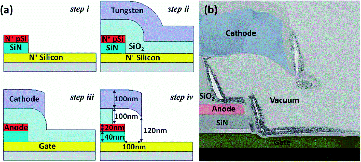 | ||
| Fig. 1 (a) Schematic illustration of the fabrication steps for the upside down vertical vacuum field emission gated diode with an umbrella cathode and (b) cross-sectional TEM image of the fabricated device. The terminals are artificially colored for contrast and better view. | ||
The dimensions of the device are labeled in the step iv panel of Fig. 1a. The thicknesses of the gate, anode and cathode are 100 nm, 20 nm and 100 nm respectively. The spacer distances are 40 nm between the gate and anode and 100 nm between the anode and cathode. The separation of the cathode and gate is 120 nm and the overhang of the cathode over the anode is 100 nm. These dimensions are not necessarily optimal, as no attempt was made to optimize the performance with an extensive parametric study.
Results and discussion
Fig. 1b shows a TEM cross-sectional view of the fabricated device. The gate, cathode and anode terminals are artificially colored for better view and contrast. The cathode is bent downward so that the emitting surface is facing the gate. The bending of the cathode is attained by conformally following the corner region of SiO2 underneath. The edge of the cathode becomes like a bird's beak when patterning is made over the SiO2 corner. As a result, a sharp emitter is attained only with the topology of the rounded film. The electron emission region here resembles a rim shape around the edge of an umbrella-like cathode. Whereas the conventional ordinary needle-like cathode yields a pointed beam, the rim-like cathode here yields a cylindrical beam as shown in the simulation results of Fig. 2. The anode voltage is applied to extract the electrons from the cathode, which yields diode characteristics as will be seen later. The gate voltage can also affect the electric field near the emitter, which results in the shift of the diode characteristics.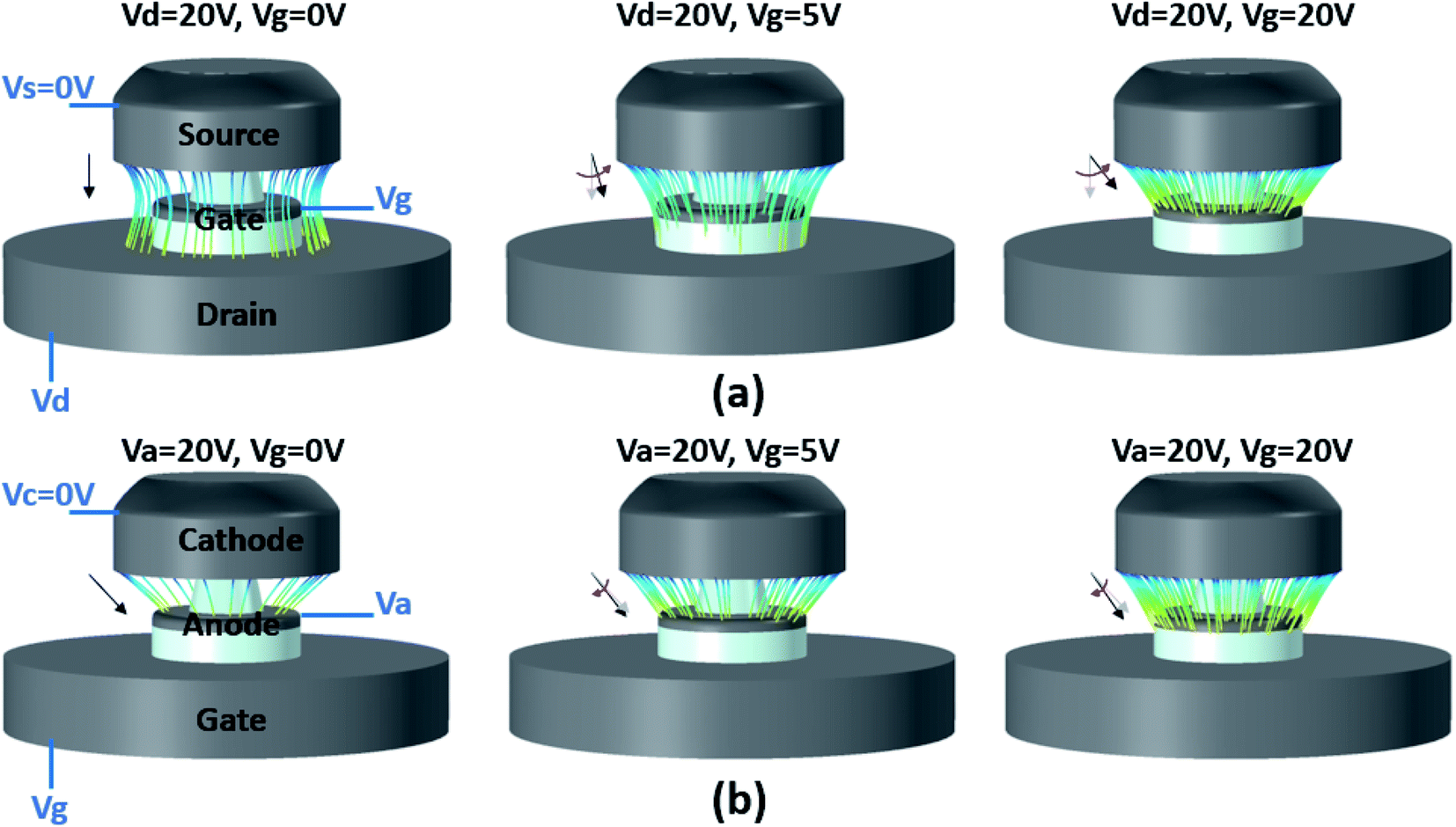 | ||
| Fig. 2 Electron trajectory simulation results for three stages: off-state, sub-threshold and on-state. (a) VFET – traditional configuration of the gate that is placed between the source and drain in a transistor and (b) VFEGD – proposed configuration of the gate that is placed below the cathode and anode. | ||
Fig. 2 shows the results from the electron propagation trajectory simulation of the umbrella cathode VFEGD with conventional and proposed terminal assignments. A finite element solver, COMSOL Multiphysics was used for the simulation. The simulated device dimensions are the same as in the fabricated device shown in Fig. 1. All the material and model parameters were set at the default values in the Multiphysics solver. Fig. 2a shows the traditional VFET where the gate is sandwiched between the source and the drain as in any transistor. Fig. 2b is the proposed VFEGD with the gate placed under the anode. At the off-state (Vg = 0 V), the off-state leakage electrons in both devices are collected on the drain or anode terminal. The trajectory in Fig. 2a is strongly bent undesirably towards the gate electrode as the gate voltage Vg increases with an increased electric field in that direction consequently attracting electrons. As a result, the gate leakage can significantly increase with Vg and the gate current can even be greater than the drain current when the gate is located in the middle of the channel. In Fig. 2b, however, the electron trajectory stays towards the anode direction even when Vg increases. The gate leakage current can be minimal when the gate is located under the anode; the anode captures most of the electrons before they reach the gate, which is reflected in the current–voltage (I–V) behavior discussed below.
Fig. 3 and 4 show the measured current–voltage characteristics of the umbrella-like cathode device explained in Fig. 1 and 2. The same curve can be interpreted in two different ways, i.e. behavior of the gated-diode (VFEGD) or the transistor (VFET), depending on how the terminal is defined as illustrated in Fig. 2a and b. The umbrella-like cathode on top is always the electron emitter or source. When the device is considered as a VFEGD, the middle n+ polySi and the bottom n+ Si become the anode and the gate, respectively. When the device is read as VFET, the middle n+ polySi and the bottom n+ Si become the gate and the drain, respectively. Fig. 3a and b respectively show the anode current versus gate voltage (Ia–Vg) and anode current versus anode voltage (Ia–Va) characteristics measured from the VFEGD shown in Fig. 2b. When the same device and measured characteristics are read as VFET, Fig. 3a is then regarded as gate current versus drain voltage (Ig–Vd) and Fig. 3b is the gate leakage current versus gate voltage (Ig–Vg) as illustrated in Fig. 2a. The high current in Fig. 3 indicates large gate leakage for the traditional terminal mode and VFET, which has been reported before4,5,14 with gate leakage even as much as 10% of the drain current.5 In addition, when the device is considered as a VFET, Fig. 3a shows an incomplete shut-off and an on-state to off-state current ratio of 2 for Vd = 20 V and 50 for Vd = 10 V. Thus, these characteristics are not ideal for the transistor mode. However, when the device is considered as a diode, the observed anode current and its dependence on the anode voltage are as expected.9–13Fig. 3b shows a typical diode curve with no current flowing below the turn-on voltage. Electron emission occurs above the diode turn-on voltage through the Fowler–Nordheim tunneling mechanism.15 This switching feature can be utilized in diode–diode logic, rectifiers, clamps and circuit breakers. The turn-on voltage (defined as the voltage needed to generate 1 nA anode current) is approximately 7.8 V, which is determined by the work function of the cathode and device geometry. Further device miniaturization and use of low work function cathode16 can lower the turn-on voltage. The diode turn-on voltage is also modulated by the gate voltage. Comparing the diode curve at Vg = 10 V, the diode turn-on voltage is reduced by approximately 400 mV from Vg = 20 V. Such diode turn-on voltage modulation by gate voltage could be useful when fine-tuning is necessary in order to compensate for any process and temperature induced variability. Table 1 provides a comparison of the present results with vacuum diodes previously reported in the literature, indicating comparable performance of our fabricated device.
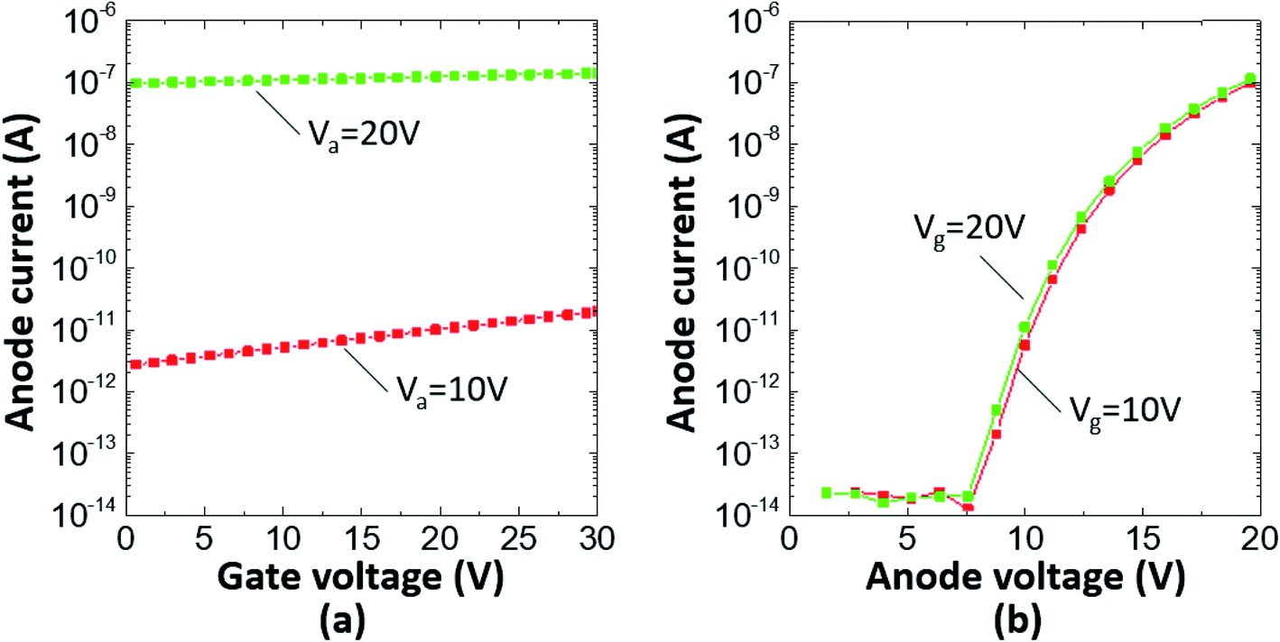 | ||
| Fig. 3 Measured device characteristics. (a) Anode current versus gate voltage and (b) anode current versus anode voltage for the proposed terminal assignment shown in Fig. 2b. | ||
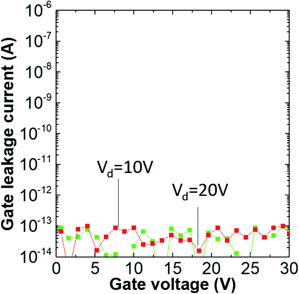 | ||
| Fig. 4 Measured gate current versus gate voltage for the proposed terminal assignment shown in Fig. 2b. | ||
| Cathode | Channel gap, nm | Turn on voltage | Anode current | Ref. |
|---|---|---|---|---|
| a Indicates availability of multiple values for the gap in the cited work. b Current was deliberately limited to this value to avoid overheating. | ||||
| SiC | 100a | 3.2 V | 22.3 nA@5 V | 8 |
| VO2 | 10 | 0.5 V | 53 μA@1 V | 9 |
| Cu | 20a | 1.75 V | 32.5 nA@5 V | 10 |
| Al–Si–Cu (0.995 Al) 4 × 4 μm | 60 | — | 24.6 μA@10 V | 11 |
| SnSe anoflower | 100 | 0.4 V | 550 A cm−2@0.75 V | 12 |
| Tungsten | 95 | 13.0 | 100 nAb | 4 |
| Tungsten | 100 | 7.8 V | 100 nA@20 V | This work |
A slightly weak dependence of the anode current on the gate voltage in the VFEGD mode is due to the large separation between the cathode and the gate here. A noticeable benefit on the other hand is that the device is intrinsically free from gate leakage. Fig. 4 shows the gate leakage current versus gate voltage characteristics. This sample plot can also be considered as the drain current versus drain voltage characteristics for the traditional VFET mode. Very low gate leakage in Fig. 4 can be translated into no drain current occurring in the VFET mode as all the electrons are intercepted by the gate as illustrated in Fig. 2a. In other words, no gate current is seen in the proposed diode mode as all of the field emission current is dominantly collected by the anode, as illustrated in Fig. 2b. Furthermore, no static power consumption is involved for biasing the gate as evidenced in Fig. 4.
The extent of gate modulation of the diode current could be controlled by device optimization. For example, the overhang distance of the emission edge and its vertical extension length could be a knob. This will make the emission surface closer to the gate but not too aggressively for emission current to be intercepted by the gate. By doing so, the gate with zero volt will be efficient enough to shut-off the anode current; consequently the on- and off-anode current ratio would be several orders of magnitude higher, and then the same architecture could be used as a transistor.
Conclusions
An upside down vertical vacuum field emission gated diode with an umbrella cathode was proposed in this work. The umbrella-shaped cathode with sharp edges was fabricated by simple deposition and etching processes. Unlike in the traditional transistor terminal arrangement, the locations of the drain and the gate are swapped so that the gate is placed at the bottom with the cathode (source) placed at the top, and the anode (drain) is sandwiched between the above two terminals. This structure features nearly zero gate leakage current, thus overcoming a common problem in miniaturized vacuum electronics devices. This silicon based architecture could be readily fabricated on a wafer scale using a standard integrated circuit manufacturing process as demonstrated here.Author contribution
J.-W. H. designed the experiments and performed device fabrication and characterization. M.-L. S. assisted with the simulations. M. M. contributed to the analysis and all authors contributed to manuscript preparation.Conflicts of interest
The authors declare no competing financial interest.Acknowledgements
This work was supported by the NASA Space Mission Directorate (SMD) and the authors thank Quang-viet Nguyen and Gary Hunter for their support of this work.References
- J. W. Han, M. L. Seol, D. I. Moon, G. Hunter and M. Meyyappan, Nat. Electron., 2019, 2, 405–411 CrossRef CAS.
- J. W. Han, D. I. Moon and M. Meyyappan, Nano Lett., 2017, 17, 2146–2151 CrossRef CAS.
- S. Nirantar, T. Ahmed, G. Ren, P. Gutruf, C. Xu, M. Bhaskaran, S. Walia and S. Sriram, Nano Lett., 2018, 18, 7478–7484 CrossRef CAS.
- L. B. De Rose, A. Scherer and W. M. Jones, IEEE Trans. Electron Devices, 2020, 67, 5125–5131 CAS.
- X. Wang, Z. Shen, S. Wu and J. Zhang, Solid-State Electron., 2017, 132, 1–5 CrossRef CAS.
- J. Xu, Y. Qin, Y. Shi, Y. Yang and X. Zhang, Nanoscale Adv., 2020, 2, 3582–3587 RSC.
- W. T. Chang, M. C. Cheng, T. Y. Chuang and M. Y. Tsai, Nanomaterials, 2020, 10, 2378 CrossRef CAS.
- J. W. Han, M. L. Seol, J. S. Kim and M. Meyyappan, ACS Appl. Nano Mater., 2020, 3, 11481–11488 CrossRef CAS.
- M. Liu, T. Li and Y. Wang, J. Vac. Sci. Technol., B: Nanotechnol. Microelectron.: Mater., Process., Meas., Phenom., 2017, 35, 031801 Search PubMed.
- M. Liu, W. Fu, Y. Yang, T. Li and Y. Wang, Appl. Phys. Lett., 2018, 112, 093104 CrossRef.
- M. Liu, Y. Yang, T. Li and Y. Wang, Micro Nano Lett., 2017, 12, 897–900 CrossRef CAS.
- W. T. Chang, H. J. Hsu and P. H. Pao, Micromachines, 2019, 10, 858 CrossRef.
- H. D. Nguyen, J. S. Kang, M. Li and Y. Hu, Nanoscale, 2019, 11, 3129–3137 RSC.
- W. T. Chang and P. H. Pao, IEEE Trans. Electron Devices, 2019, 66, 3961–3966 CAS.
- K. L. Jensen, Introduction to the Physics of Electron Emission, Wiley, 2017 Search PubMed.
- J. Kim, H. W. Oh, J. S. Kim, R. H. Baek, J. W. Han, M. Meyyappan and J. S. Lee, J. Vac. Sci. Technol., B: Nanotechnol. Microelectron.: Mater., Process., Meas., Phenom., 2017, 35, 062203 Search PubMed.
| This journal is © The Royal Society of Chemistry 2021 |