
 Open Access Article
 This Open Access Article is licensed under a Creative Commons Attribution-Non Commercial 3.0 Unported Licence
Low reflectance of carbon nanotube and nanoscroll-based thin film coatings: a case study†
Sonia
Saini
ab,
S.
Reshmi
c,
Girish M.
Gouda
b,
Ajith
Kumar S.
b,
Sriram
K. V.
b and
K.
Bhattacharjee
 *ac
*ac
aIndian Institute of Space Science and Technology (IIST), Thiruvanthapuram, 695 547, India. E-mail: kbhattacharjee@iopb.res.in; kuntala.iopb@gmail.com
bLaboratory for Electro-Optics Systems (LEOS), Indian Space Research Organization (ISRO), Bengaluru, 560 058, India
cInstitute of Physics, Sachivalaya Marg, Bhubaneswar 751 005, Odisha, India
First published on 15th March 2021
Abstract
Research on carbon material-based thin films with low light reflectance has received significant attention for the development of high absorber coatings for stray light control applications. Herein, we report a method for the successful fabrication of stable thin films comprised of carbon nanotubes (CNTs) and nanoscrolls (CNS) on an aluminium (Al) substrate, which exhibited low reflectance of the order of 2–3% in the visible and near-infrared (NIR) spectral bands. Changes in the structural and chemical composition of pristine single-walled carbon nanotube (SWCNT) samples were analyzed after each processing step. Spectroscopy, microscopy and microstructural studies demonstrated emergence of CNS and multi-walled carbon nanotubes (MWCNTs) due to the sequential chemical processing of the sample. Transmission electron microscopy (TEM) and scanning electron microscopy (SEM) studies revealed the formation of CNS via curling and folding of graphene sheets. Microstructural investigations including SEM and atomic force microscopy (AFM) confirmed the presence of microcavities and pores on the surface of the film. These cavities and pores significantly contribute to the observed low reflectance value of CNTs, CNS compound films by trapping the incident light. Fundamental space environmental simulation tests (SEST) were performed on the coated films, that showed promising results with reflectance values almost unaltered in the visible and NIR spectral bands, demonstrating the durability of these films as potential candidates to be used in extreme space environmental conditions. This study describes the preparation, characterization, and testing of blended CNT and CNS coatings for low-light scattering applications.
1. Introduction
Because of the optical transitions of the π-band, carbon is considered to be a good absorber, which is used in many conventional black materials such as carbon black and graphite.1 Carbon soot has been studied extensively as a black absorber coating for low-cost and large-area applications.2–4 However, the emissivity of conventional carbon-based coatings is usually in the order of 0.80–0.85 due to reflection at the air–dielectric interface, limiting their application as an absorber.5–7 In the last few years, main research interest evolved to overcome this shortcoming using carbon nanostructures,7,8 vertically aligned carbon nanotube (CNT) forests, etc.1,2,4–6 CNTs with their 1D structure, confined electron density to the plane of the rolled graphite sheet and the excitonic optical transitions across sharp one-dimensional (1D) density of states show great promise as black absorber coatings.1–4,11 The development of CNT-based black absorber thin films has become an advanced field of research recently, which depends on the intrinsic properties of CNTs and the potential light-trapping ability of CNT films. Since their discovery by Sumio Iijima8 in 1991, CNTs have shown enormous technological importance15–17 owing to their exotic physical and chemical properties.10,18 CNTs, classified as single-walled (SW) and multi-walled (MW), are comprised of a hexagonal lattice of carbon (C) atoms with a high surface area and aspect ratio.19 SWCNTs, structurally the simplest ones, have only one atomic layer of sp2 hybridized C atoms folded in a cylindrical symmetry.10 They are uniquely determined by their chiral vectors, energetically very stable under normal conditions, and can show robust mechanical strength associated with high toughness and elastic moduli.20–23 Conversely, MWCNTs are considered the nested SWCNTs of seamlessly rolled multiple graphene layers forming concentric tubes, whereas carbon nanoscrolls (CNS) are rolled graphene sheets in the form of a spiral 1D structure, offering a distinctively different configuration and complexity. The van der Waals (vdWs) interaction between the layers of MWCNTs and CNS provides structural stability by binding layers to maintain their respective shapes. CNS have become a recent topic of interest owing to their open-ended morphology, tunable diameter, high carrier mobility, and easy intercalation of materials between their layers, showing many properties comparable to that of MWCNTs or even superior. Furthermore, the one-dimensional nature of CNTs24 and CNS leads to anisotropy in their properties, which are better observed along the tube axis.Previous studies on CNT-based coatings include water-based growth of a uniform array of CNTs,25 spray coating of SWCNT,11 and growth of vertically aligned SWCNT forests.1,4,26,27 Additionally, there are reports on light absorption studies using CNT films fabricated via chemical vapor deposition (CVD).27,28 A very black coating of CNTs fabricated on a silicon substrate was claimed to be “the world's darkest material” with an absorptance value of 0.9997.29 CNT forests being the blackest materials1,29,30 can be useful for the fabrication of thin-film coatings for optical studies, energy conversion,31,32 antireflection,8,33 and radiometry.34,35 An important finding related to this is the wavelength-independent emissivity of the CNTs.1 Ajayan et al.29 showed that the reflectance of vertically aligned CNT forests could be as low as 0.045%, and therefore, the light-absorbing ability of these nanotube arrays can be enhanced strongly.1,29 A near-perfect absorption was observed by Shi et al. for a coating of MWCNTs on an arbitrary shape.36 They successfully devised an experiment to calculate the imaginary part of the refractive index for the CNT forest, which was obtained to be sufficiently low, validating the broadband absorption. CNTs can overpower other materials due to the fact that if aligned vertically, they remain uniformly black for a range of wavelengths throughout the visible and far-infrared regions.3 These properties make CNTs the most suitable candidate for stray light control applications. In a comparative study conducted by Mizuno et al.,1 it was reported that vertically aligned CVD-grown SWCNTs showed more emissivity than the spray-coated sample, confirming the structure-dependent black body behavior (i.e., higher absorption) of the SWCNTs. They reported approximately 0.98% emissivity in the case of vertically grown SWCNT on Si substrates.1 However, the vertical alignment of the CNTs can be associated with angle- and polarization-dependent selective light reflections and the related sensitivity associated with mechanical aggregations.37 Accordingly, a direct solution to this problem can be films with a random orientation of CNTs; however, this will compromise the overall reflectivity of the coatings.
In addition to the broadband, high optical absorptance value, the most important aspect of using CNTs is the ability to produce them easily on flexible substrates. The substrate plays an important role in modulating the different optical properties of CNT forests such as the morphology, surface roughness, forest height, and forest density, which will highly affect the emissivity of the CNT film coatings.38 Aluminum (Al) sheets, which are light weight, flexible, ductile, cost effective, and abundantly available, are good conductors, and thus considered promising substrate materials for applications in flexible electronics.39,40 To fabricate CNT-based flexible conductive electrodes, the CVD technique is widely explored; however, it requires harsh deposition conditions such as high substrate temperature, various precursors, and reaction chamber, which make the process complicated. Also, exceptional diffuse reflectance has been reported earlier for CVD-grown layers of CNTs,41 posing limitations in terms of specific growth conditions such as high temperature, thereby making it incompatible with Al or thin titanium substrate surfaces, which are commonly used in space-related applications. It has been reported that the fabrication of SWCNT films via a simple spraying approach of a colloidal suspension on the substrate and subsequent heating42 of the film to evaporate the dispersing fluid can yield films with high uniformity43 and stability. However, an important step in the process is the synthesis of the colloidal suspension, which is a significant exercise due to the low dispersibility of CNTs bound by attractive vdWs force. Consequently, there are technical difficulties and challenges in developing a stable, homogenous suspension, which can be achieved by adsorbing adequate surfactants on the sidewalls of the CNTs, mechanically debundling them by sonication, and using a proper binder to achieve uniform, stable coatings.
Although significant research has been carried out and is still ongoing with respect to the optical absorption of CNT thin films and forests, there is hardly any knowledge on the light absorption of CNS. Theoretical calculations show that under the influence of a transverse electric field, the optical absorption spectra of CNS manifest distinguished peak features owing to their 1D structure, which are strongly dependent on the geometry of the CNS and the applied field strength.44 A UV-visible optical absorption spectroscopy experiment carried out on a CNS sample also showed fascinating features.45 Consequently, CNS with their open ends and varying layer widths seem to be a promising material for use as absorber coatings.
To date, a variety of routes have been employed to fabricate CNS from graphene sheets such as mechanical methods and chemical synthesis. The molecular dynamics simulations performed by Braga et al. showed that CNS can have a lower energy than graphene layers.46 The production of high yield CNS was first reported more than a decade ago via the intercalation of graphite with potassium followed by exfoliation in a highly exothermal reaction environment. Exfoliated graphene layers were then deformed by sonication to give rise to CNS.47,48 Since then, many other methods have been proposed for the bulk production of CNS, e.g., microwave irradiation49 using CNTs,50 inducing solution-based scrolling of graphene sheets on a Silicon dioxide (SiO2) substrate,48 and solvent-assisted self-assembly of graphene oxide (GO) layers.51 The formation of CNS is an energy-aided process due to the structural transition of the graphene layer, where a large overlap between two edges of freestanding graphene occurs, leading to the relative sliding of the overlapped region after a critical overlapped area is attained. The self-sustained scrolling process continues as the vdWs interactions between the layers provide structural stability to form CNS.46 Also, the low bending rigidity of graphene, which is determined by the bending-induced changes in the interactions between electron orbitals,52 plays an important role in the structural modification of graphene nanoribbons and the eventual formation of CNS. For monolayer graphene, the out-of-plane deformation associated with stretching and compression of covalent carbon–carbon bonds is responsible for the bending rigidity,53,54 while for multilayer graphene, this depends on the number of layers and the interlayer shear interaction.55 The bending stiffness typically follows a thickness-dependent square power relation for the self-folding mechanism of few-layer graphene (2–6 layers) with an interlayer shear modulus value in the range of 0.36–0.49 GPa.55 The atomistic simulations performed by Nikiforov et al.56 showed that large diameter SWCNTs very closely represent the behavior of graphene under pure bending in the low-curvature linear elastic regime. The simulations revealed curvature-induced torsional misalignment of the π hybrid orbitals as the key source of bending stiffness with a value of 1.49 eV.56 Although theoretical studies provide a wide range of values of bending rigidity for single-layer graphene,57–61 the experimental value is cited to be 1.2 eV for a graphene sheet.62
Herein, we report a facile approach for the fabrication of carbon-based thin film coatings comprised of CNTs and CNS, which exhibited a low reflectance in the order of 2–3% in the visible and NIR spectral bands. We demonstrated a process for the successful fabrication of environmentally stable and uniform CNT–CNS blended thin film coatings on flexible Al substrates using a simple, cost-effective spray coating technique. The sequential experimental observations during the process of developing these coatings starting from SWCNTs are described. Furthermore, the functional group analysis, Raman spectroscopy studies, X-ray diffraction (XRD) investigations, transmission electron microscopy (TEM) studies, spectral reflectance measurement, microstructural analysis, and space environmental simulation tests (SEST) are presented. The microstructural investigations, namely scanning electron microscopy (SEM) and atomic force microscopy (AFM) studies, carried out on the coated films provided direct mappings of the surface morphology with evidence of cavities and pores on the film surface. These cavities trap the incident light without letting it reflect immediately, and thus play an important role in the low reflectance value. The preliminary SEST conducted on the spray-coated films showed good stability with optimum performance in the presence of outer space environmental conditions, which indicate the potential of these CNT–CNS compound films as candidates for stray light control applications in spaceborne devices.
2. Experimental
SWCNTs, which were obtained from NoPo Nanotechnologies India Pvt. Ltd. Bengaluru, were produced via a high-pressure carbon monoxide (HIPCO) method63,64 and had a catalytic content of <0.05% Fe, diameter of 0.6 to 1.1 nm and length of ∼400 to 1000 nm. The morphology of the SWCNTs was a dry black powder with carbon as SWCNTs > 96%. The synthesis methods yielded nanotubes with a range of diameters and chirality, which usually contained metallic and amorphous contaminants. Therefore, post-synthesis chemical purification was required to eliminate the contaminants present in the as-prepared CNTs, which was carried out by wet oxidation at 300 °C, followed by acid wash using concentrated hydrochloric acid (HCl)65–67 and annealing at 900 °C in an inert environment.64,68 We mainly procured purified samples from NoPo Nanotechnologies. However, some SWCNTs prior to purification were also procured for verification of the nature of the raw CNTs. After purification, further experimental processing and related investigations developed and carried out by us are discussed below.2.1. Functionalization
The functionalization of CNTs was performed by adding concentrated H2SO4 and HNO3 having a volume ratio of 3![[thin space (1/6-em)]](https://www.rsc.org/images/entities/char_2009.gif) :1 to a beaker and purified CNT black powder. The mixture was stirred using a magnetic stirrer at a temperature of 70 °C for 8 h and allowed to cool to room temperature. The mixture was neutralized by rinsing with deionized water until neutral pH was obtained. The functionalized CNT powder was obtained by sieving the solution using Whatman filter paper. The powder was dried under vacuum at room temperature. A schematic of the functionalization process is shown in Fig. 1.
:1 to a beaker and purified CNT black powder. The mixture was stirred using a magnetic stirrer at a temperature of 70 °C for 8 h and allowed to cool to room temperature. The mixture was neutralized by rinsing with deionized water until neutral pH was obtained. The functionalized CNT powder was obtained by sieving the solution using Whatman filter paper. The powder was dried under vacuum at room temperature. A schematic of the functionalization process is shown in Fig. 1.
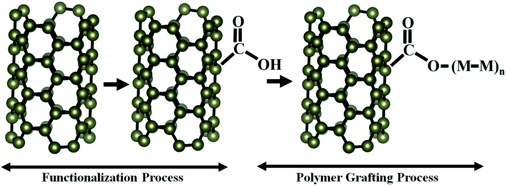 | ||
| Fig. 1 Schematic representation of the functionalization and polymer grafting processes. The attachment of carboxyl group (–COOH) after functionalization was followed by polymer grafting with hydrocarbon chains, –(M–M)n. | ||
2.2. Spray coating
The functionalized powder was mixed with a weighed amount of the organic binder polyurethane and solvent and ultrasonicated for 60 min using a Q500 ultrasonic probe sonicator from Q-Sonica to obtain a well-dispersed agglomeration-free solution. The obtained solution was spray coated [Fig. 2] on clean Al substrates using a hand airbrush Pilot AB16 in a glove box under a controlled nitrogen atmosphere. The Al substrate was preheated to a temperature of around 300 °C using a quartz radiant heater attached with a PID controller and a thermocouple to maintain the temperature within the range of 300 ± 10 °C during the spray coating process. After the deposition of the CNT film, the samples were allowed to cool to room temperature (RT). | ||
| Fig. 2 Schematic representation of the spray coating process. | ||
3. Characterization
Different characterization techniques were used to understand the processed CNT films. The purified and functionalized CNTs were subjected to functional group analysis by Fourier transform infrared (FTIR) spectroscopy. The infrared absorption spectra of the CNT pellets prepared using KBr powder were measured in the range of 4000 to 500 cm−1 using a PerkinElmer Spectrum GX spectrometer. The structural signatures of the purified, functionalized, and spray-coated samples were obtained by subjecting them to Raman spectroscopy analysis using a Lab Ram HR 800 instrument. The surface morphology of the samples was investigated by field-emission scanning electron microscopy on a Zeiss SEM Ultra55. AFM measurements were carried out using a Bruker Dimension ICON atomic force microscope in tapping mode (amplitude modulation mode), which helped minimize the effect of friction and other lateral forces in the topography measurements. High Resolution (HR) TEM measurements were carried out by drop-casting the sample on Cu grids using an FEI-Titan Themis instrument operated at 300 kV. XRD measurements were carried out using a Smartlab X-ray diffractometer by Rigaku. The data was collected using monochromatic Cu Kα radiation (1.54 Å) at 40 kV and 30 mA. The spectral properties of the spray-coated samples were analyzed using a UV-VIS-NIR spectrometer, PerkinElmer Lambda 950 in the wavelength range of 400 to 2500 nm. The spray-coated samples were subjected to SESTs using the environmental test facilities available at LEOS, Bengaluru.4. Result and discussion
4.1. Functional group analysis: FTIR study
FTIR is a versatile non-destructive technique for the identification and characterization of the chemical structure of SWCNTs. The normalized FTIR spectra of the purified and functionalized samples are shown in Fig. 3. The chemical incorporation of various functional components on the sidewalls of CNTs is visible in the FTIR investigations [Fig. 3]. It is evident that the intensities of the various bands increased compared to the purified sample [Fig. 3], together with the appearance of new bands. This indicates the successful functionalization of CNTs. The absorption feature obtained at 3393 cm−1 [Fig. 3] in the functionalized CNTs is assigned to the –OH stretching mode of the –COOH group.69,70 The bands at 2940 cm−1 and 2878 cm−1 correspond to the –CH stretching vibrations.71 The peaks and hump-like characteristics observed in the FTIR spectrum between 2734–1734 cm−1 mainly correspond to aldehyde (2750 cm−1,![[double bond, length as m-dash]](https://www.rsc.org/images/entities/char_e001.gif) C–H stretching mode); weak signature of nitrile (2250 cm−1, –C
C–H stretching mode); weak signature of nitrile (2250 cm−1, –C![[triple bond, length as m-dash]](https://www.rsc.org/images/entities/char_e002.gif) N band, which can be due to the presence of a small amount of nitrogen in the sample during treatment with HNO3); weak presence of alkyne (2150 cm−1, –CC– band) and strong signature of –CO stretching (1734 cm−1). The weak absorption peaks observed in the range of 1726–1818 cm–1 can be assigned to the –CO stretching within the anhydride group [–(CO)2O]. The relatively strong peak feature centered at 1626 cm−1 is assigned to the stretching of the CC graphitic group.72 The prominent and comparatively broad absorption peak seen at 1375 cm−1 is attributed to the –C–O stretching, corresponding to the carboxylic group. The most intense peak at 1067 cm−1 is associated with the –C–O alkoxy group stretching, whereas, the small absorption band at 671 cm−1 is ascribed to the –CO group stretching.71,72 The evidence of some bands present in the purified sample before functionalization indicates the possibility of the corresponding chemical species being incorporated in the CNTs during the acid purification process.
N band, which can be due to the presence of a small amount of nitrogen in the sample during treatment with HNO3); weak presence of alkyne (2150 cm−1, –CC– band) and strong signature of –CO stretching (1734 cm−1). The weak absorption peaks observed in the range of 1726–1818 cm–1 can be assigned to the –CO stretching within the anhydride group [–(CO)2O]. The relatively strong peak feature centered at 1626 cm−1 is assigned to the stretching of the CC graphitic group.72 The prominent and comparatively broad absorption peak seen at 1375 cm−1 is attributed to the –C–O stretching, corresponding to the carboxylic group. The most intense peak at 1067 cm−1 is associated with the –C–O alkoxy group stretching, whereas, the small absorption band at 671 cm−1 is ascribed to the –CO group stretching.71,72 The evidence of some bands present in the purified sample before functionalization indicates the possibility of the corresponding chemical species being incorporated in the CNTs during the acid purification process.
 | ||
| Fig. 3 FTIR spectra of purified and functionalized samples. Both the spectra are normalized with respect to the maximum intensity of the purified sample data. | ||
4.2. Structural analysis: Raman studies
Raman measurement, which is very sensitive to the chiral indices (n and m), is naturally considered to be an important spectroscopic tool to characterize CNTs. The normalized Raman spectra of the purified, functionalized, and coated film are shown in Fig. 4. We observe a clear signature of the defect-induced D band together with the characteristic G and 2D (G′) features in the acquired Raman spectra of the samples [Fig. 4]. Evidence of the characteristic radial breathing modes (RBMs) of SWCNTs is seen only in the purified sample. All these bands are marked in Fig. 4. The RBMs, which are associated with the Ag symmetry of the carbon atoms moving in-phase in the radial direction, are unique to SWCNTs and usually occur in the range of 120 to 350 cm−1 for tubes with a diameter ranging from 0.7 to 2 nm.73 We observe the manifestation of RBMs in the purified sample between 150 and 350 cm−1 [Fig. 4(a)].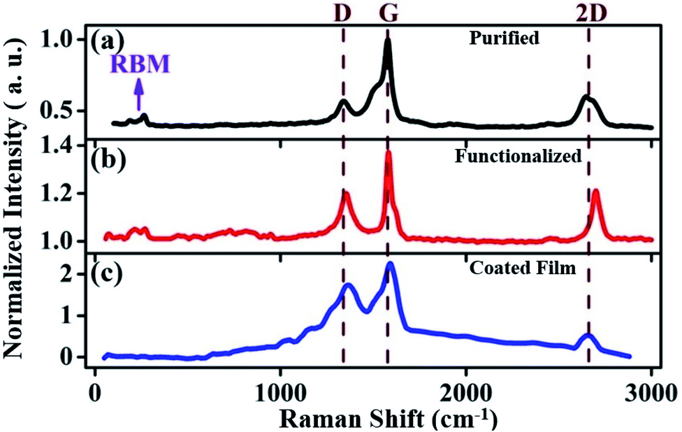 | ||
| Fig. 4 Raman spectra of (a) purified, (b) functionalized and (c) coated film. The spectra are normalized with respect to the G peak of the purified data shown in (a). | ||
The curve fitting of the RBMs performed with Lorentz oscillators reveals signature of 16 components [Fig. 5]. These components can be associated with different nanotube species of non-identical diameter and chirality present in the CNT bundle. The diameter, d, of the tubes is calculated using the simple monotonic equation,74
 | (1) |
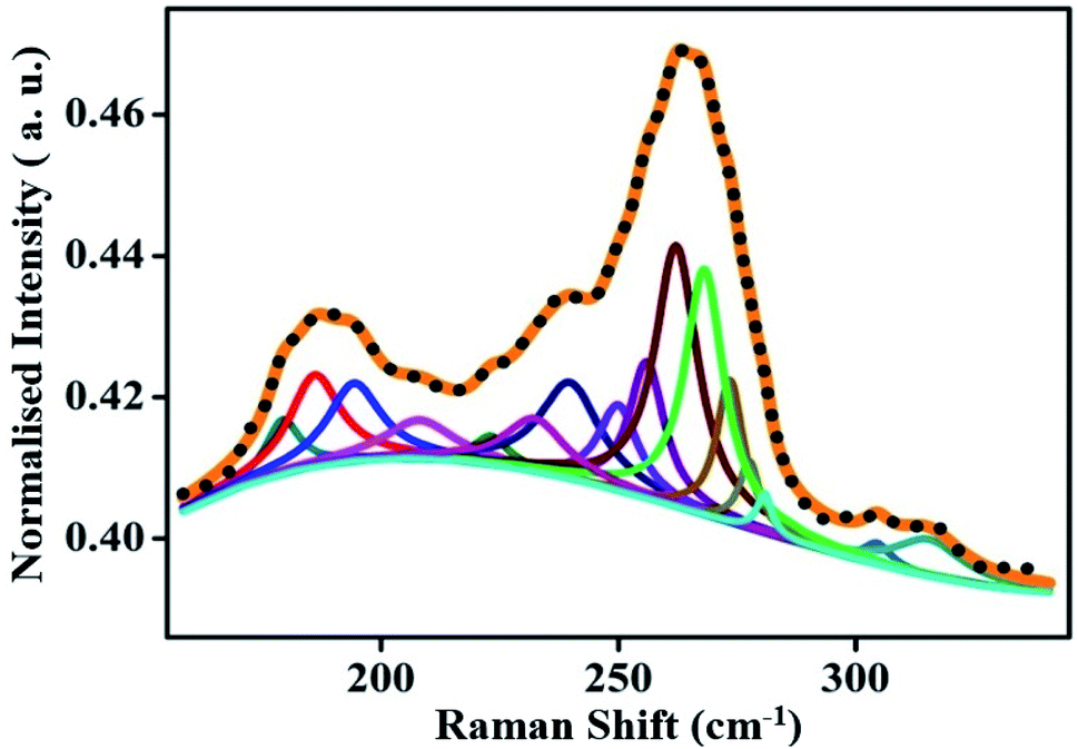 | ||
| Fig. 5 Fitted RBM of the purified sample, revealing the signatures of the various nanotube species. The intensity of the spectrum was normalized with respect to the G peak of the purified data. | ||
| RBM frequency (cm−1) | Diameter (nm) |
|---|---|
| 315.4 | 0.74 |
| 304.5 | 0.76 |
| 280.7 | 0.83 |
| 277.7 | 0.84 |
| 273.5 | 0.86 |
| 268.2 | 0.87 |
| 262.2 | 0.89 |
| 256 | 0.92 |
| 250 | 0.94 |
| 239.8 | 0.98 |
| 232.5 | 1.02 |
| 223.2 | 1.06 |
| 208.1 | 1.14 |
| 194.3 | 1.23 |
| 186.1 | 1.29 |
| 179.3 | 1.34 |
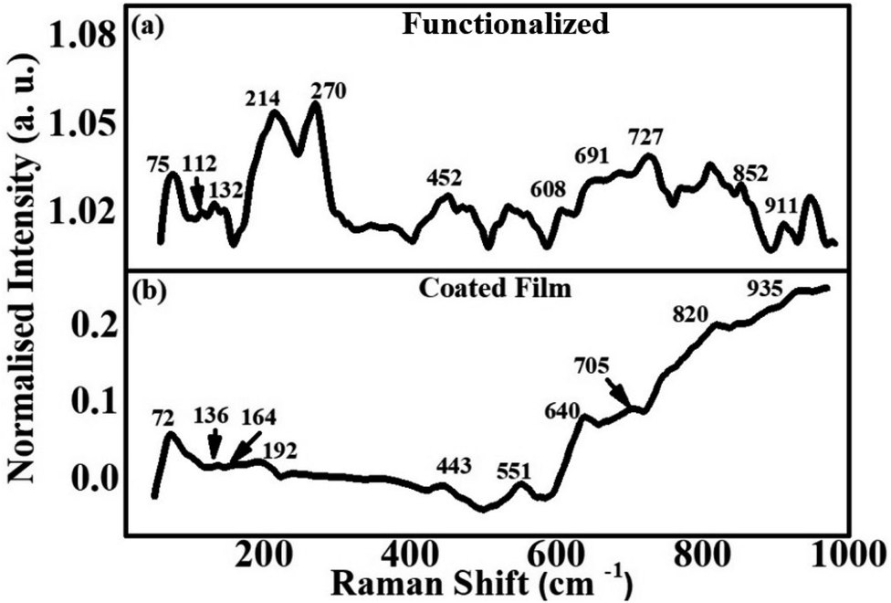
A close analysis of the low-frequency range in the Raman spectra of the functionalized and coated samples (up to 1000 cm−1) reveal many peak onsets. It was reported that curved graphene sheets can show Raman signatures in the range of 200–1000 cm−1.75–77 For the functionalized sample, the low-frequency range of 50–1000 cm−1 is analyzed. RBM-like features together with several onsets related to the CNS and MWCNT components [Fig. 6(a)] are observed in the spectrum [Fig. 6]. The features located at around 270, 727, and 852 cm−1 can be associated with the curvature happening in the graphene sheets during the functionalization process,76 whereas the peaks appearing at around 452, 608, 691, and 911 cm−1 correspond to CNS75 [Fig. 6(a)]. The transverse optic and transverse acoustic phonon branches, which are usually inactive in the crystalline planar graphite, can become active due to the relaxation of the Raman selection rules owing to the curvature of the scrolls.75 The Raman modes related to single and multi-wall CNTs are also observed in the range 50 to 220 cm−1.77,78 For the MWCNTs, the origin of the low-frequency bands is due to the breathing vibrations corresponding to individual walls, a phenomenon similar to that of the RBMs in SWCNTs. However, the vibration in MWCNTs is quite complex due to interaction among the individual concentric walls. We identify the characteristic onsets corresponding to MWCNTs at around 75, 112, 132, and 214 cm−1,78 which can be associated with the concentration of emerging MWCNTs after the functionalization process.78 The coated sample also exhibits almost a similar trend with the low-frequency peaks appearing at 72, 136, 164, and 192 cm−1, signifying MWCNT components in the film,78 while the onsets at 443, 640, 705, and 935 cm−1 correspond to CNS.78 We also observe several additional weak low-frequency Raman onsets, which can be attributed to the curving of the graphitic sheets75 [Fig. 6(b)]. A diameter-dependent shift in the high-energy phonons can happen to the curved graphene layers and it is even possible to observe additional phonon modes corresponding to the extra symmetries induced in the curved structures.79
 | ||
| Fig. 6 Low-frequency Raman spectra from (a) functionalized and (b) coated samples. The intensity of both spectra was normalized with respect to the G peak of the purified data. | ||
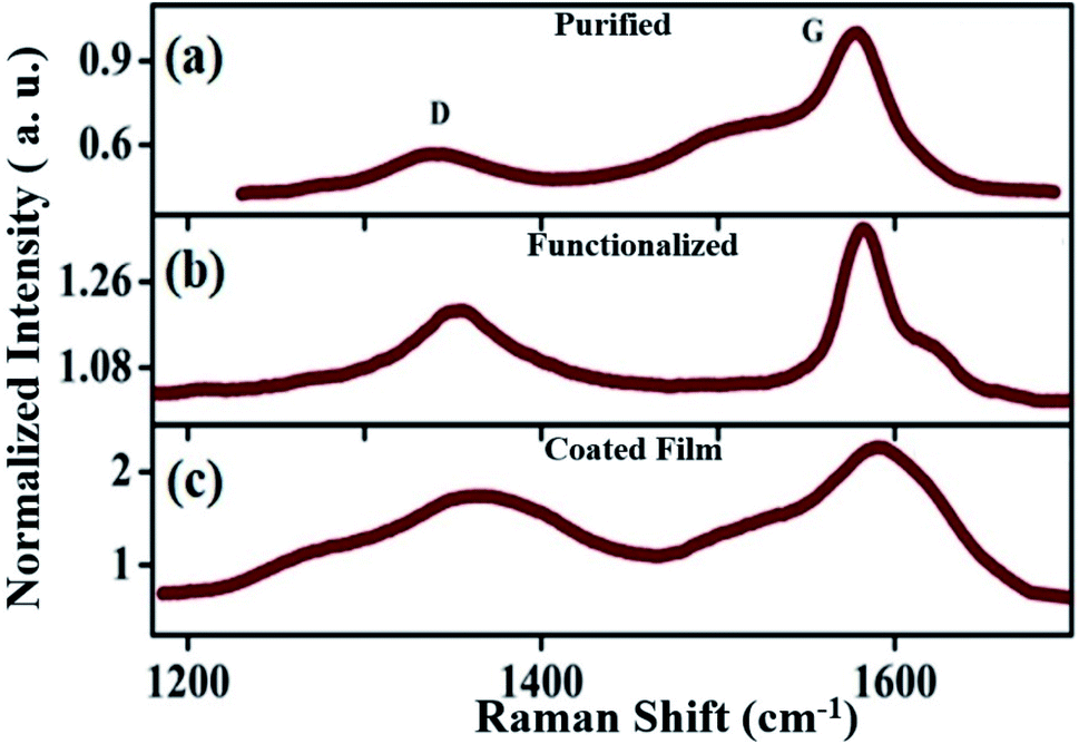
We observe clear evidence of the D, G, and 2D band signatures in our samples. The graphitic tangential mode or G band corresponds to an optical phonon mode, while the 2D band is a Raman-allowed signature by symmetry, not defect induced.80 The D peak, which corresponds to the breathing modes of the A1g symmetry around the K points of the Brillouin zone, is forbidden in an ideal graphitic structure and requires structural defects for a phonon of certain angular momentum to be activated. Consequently, the signature of the D band is a measure of the non-crystalline disorder, lattice distortions, and defects associated with the CNTs, whereas a higher intensity of the G band compared to D is a manifestation of superior graphitic crystallinity in the sample.
Further confirmation of the formation of CNS and MWCNT can also be drawn from the D, G, and 2D bands. The presence of CNS and gradual induction of defects on the sidewalls of the raw SWCNTs during the processing treatment74,81 can be directly associated with the D peaks, which consequently exhibit an increase in intensity [Fig. 7] and full width at half maximum (FWHM) (59.7, 65.84, and 149.29 cm−1) [Fig. 7] from the purified sample to the coated film. CNS with their long unfused edges contribute to enhancing the D peak intensity.75 The clear up-shift in the D peak positions (1343.66, 1353.79, and 1363.52 cm−1) indicates an increase in the diameter of the curved-sheets/nanoscrolls/nanotubes from the purified to the coated film. The intensity ratio of the G to D band (IG/ID) decreases after functionalization, which is attributed to the distortion in the graphitic structure, elongation of the C–C bond due to the electron transfer, and increase in the sp3 C hybridization in comparison to the sp2 C.81–84 The purified sample shows the lowest [Fig. 7(a)] D band intensity (ID) and highest IG/ID ratio, while the coated film has the most intense D feature [Fig. 7(c)] with the smallest IG/ID value. The IG/ID ratio of the functionalized sample [Fig. 7(b)] is in the middle. The position of the G band is also important, which is highly dependent on the elastic strain. Due to the rolling and curling of the sheets, elastic strain develops in the system, which has an inverse relation to the diameter of curvature.75 Consequently, a downward shift in the G peak position can occur with an increase in the diameter of the rolled sheets. A small down-shift and broadening of the G band is observed for the coated film compared to that of the functionalized sample, indicating the presence of a larger diameter of curvature and varying elastic strain, respectively, in the sample. Acid treatment of the graphitic sheets can affect the peak position and the peak width.75 Furthermore, the broadening of the 2D band also signifies a greater number of layers stacked on the wall. The broadening of the 2D band is greater for the coated sample compared to the functionalized sample.
 | ||
| Fig. 7 D and G mode vibrations in (a) purified, (b) functionalized and (c) coated samples. The intensity of the spectra was normalized with respect to the G peak of the purified data shown in (a). | ||
Further analyses are carried out on the D, G, and 2D signatures by considering approximations, and the results obtained are shown and discussed in detail in the ESI.† Our analysis on the D bands showed various defect components [Fig. S1†], whereas the 2D bands clearly exhibit the presence of single-layer graphene-like structures in the nanotube ensembles (with the highest intensity), together with various double electron-phonon resonant processes [Fig. S3 see ESI†]. We have performed G band fitting by considering both the Lorentz profiles [Fig. S1†] and a combination of Lorentz and Breit–Wigner–Fano (BWF) line shapes [Fig. S2†]. Our investigations on the G band features do not reveal any signature of metallic CNTs in the samples, which may be an indication that the metallic tubes are not in resonance with the 2.33 eV laser excitation energy used for the Raman measurements herein.
4.3. X-ray investigation
The XRD investigations carried out on the CNT samples are shown in Fig. 8. The characteristic (002) peak of the carbon-based materials is observed [Fig. 8] at around 26°. The intensity and width of the (002) peak (JCPDS card no. 01-075-1621) are related to the number of layers, the orientation of the CNTs, and the content network distortion.85 The high intensity of the (002) peak and small value of the FWHM [Fig. 8(a and b)] indicate the high crystalline quality of the purified and functionalized samples. The XRD pattern of the purified CNTs [Fig. 8(a)] also exhibits peaks at around 42° and 44°, corresponding to the (100) and (101) planes of graphitic carbon (JCPDS card no. 01-075-1621) [Fig. 8(a)], which can be attributed to the inter-shell spacing of the concentric graphene sheets of multiwalled CNTs.64 In addition, the peak-like features at 33.5° and 36.2° (indicated in the images by stars) in the purified sample can be associated with the Fe catalyst impurities,64 that got attached to the CNTs during the HIPCO process,86 while the peaks at 54.6° and 77.5° correspond to the (004) and (110) planes of the graphitic layers (JCPDS card no. 01-075-1621). The XRD data obtained for the functionalized sample is shown in Fig. 7(b). We could hardly find any difference in the peak positions of the graphitic planes between the purified and the functionalized samples; however, a variation in the intensity of the peaks is observed, which can be associated with the further de-bundling and better dispersion of the CNTs in the functionalized sample. The XRD data of the coated film exhibit signatures of the graphitic components and the Al substrate. The graphitic planes of (002) and (101) at 26° and 44.6° respectively, are observed with a lower intensity compared to that of the functionalized sample. Generally, the polymer grafting process of the coated film will lead to an apparent decrease in the intensity of the graphitic planes.87,88 The peaks at 38.3°, 78.1°, and 82.3° are assigned to the (111), (311), and (222) planes of the Al substrate, respectively.89 The broad onset peak at around 18° is attributed to the presence of the CNS component in the sample.89 It has been reported that due to the residual solvent trapped between the CNS layers, there may be an expansion in the interlayer spacing, giving rise to a distribution that contributes to a broad onset of around 15–18°.89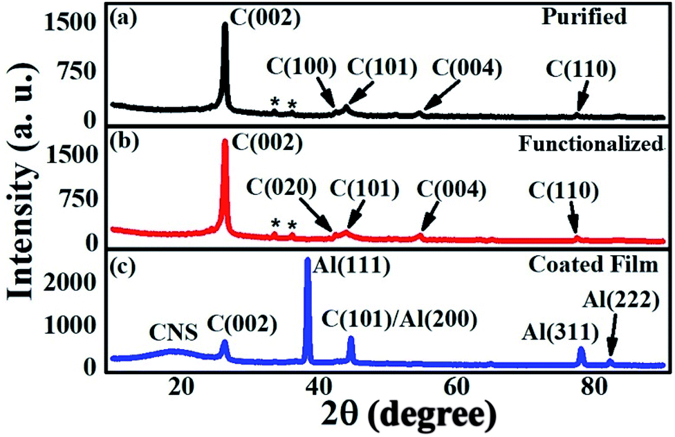 | ||
| Fig. 8 XRD plots of (a) purified, (b) functionalized and (c) coated film. | ||
4.4. Electron microscopy investigations
Fig. 9–11 and S4 (in the ESI†) display the TEM images. An artificial color code is given to all the images for better visualization, which is done during the analysis of the data using ImageJ/Gwyddion. A large-area TEM micrograph of the as-prepared SWCNT bundles prior to purification is shown in Fig. S4(a).† The pristine sample shows sparse bundle network of SWCNTs [Fig. S4†] together with traces of carbonaceous particles [marked by arrows in Fig. S4(a)†] and metal catalyst particles, which appear as dark spots in Fig. S4(b–d).† The SWCNTs forming bundles in the as-prepared sample are shown and marked by white arrows in Fig. S4.† We do not find any evidence of MWCNTs or CNS in the pristine sample during our TEM studies.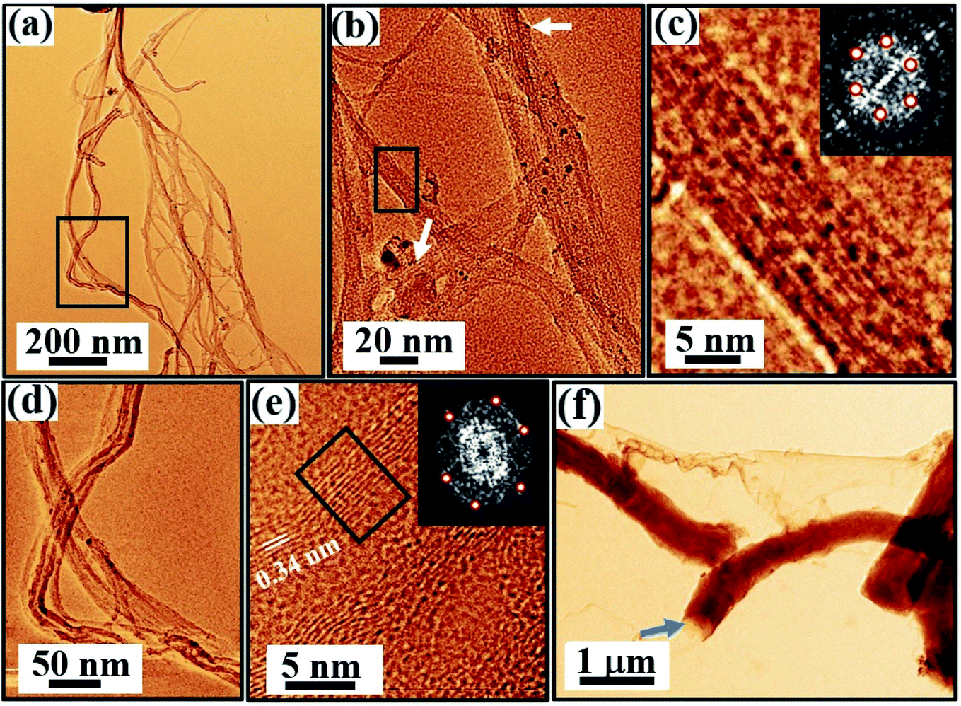 | ||
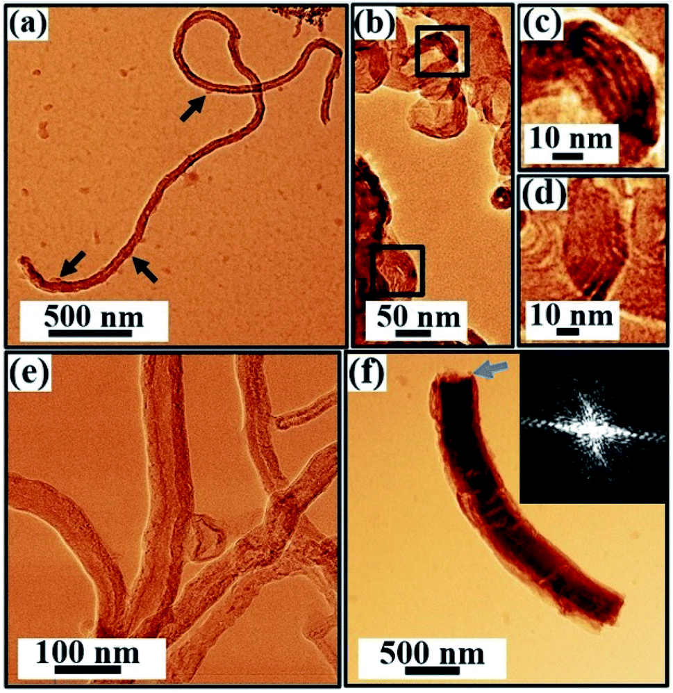
| Fig. 9 TEM investigations of the purified sample. (a) Large-scale image showing sparse bundle network of SW and MW CNTs with rare presence of impurity particles. (b and c) Evidence of SWCNTs in the bundles is shown and marked by arrows. Inset of (c) shows the hexagonal symmetry from the SWCNT bundle. (d) MWCNTs from the marked area in (a). (e) High-resolution TEM image of an MWCNT with graphitic (002) plane stacking. The (002) layer spacing of ∼0.34 nm is marked in (e). Inset of (e) is the FFT from the selected area [marked as a rectangle in the image]. (f) Folding of the carbon sheets to form CNS. The open end of CNS is marked with an arrow. | ||
 | ||
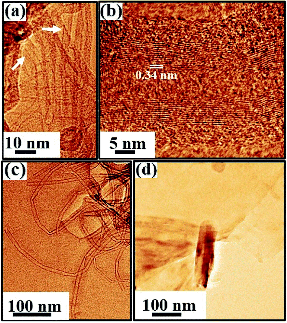
| Fig. 10 TEM micrographs of the functionalized sample. (a) Attachment of functional groups on the sidewalls of the tubes [marked with arrows]. (b) Evidence of SWCNT bundles after the functionalization process. Two regions in (b) [marked with squares], which show the clear periodic alignment of SWCNTs are zoomed and shown as (c) and (d). Amorphous walls of the MWCNTs can be seen in (e). A nanoscroll with an open-end [marked with arrow] is shown in (f). Inset: FFT of the CNS. | ||
 | ||
| Fig. 11 TEM investigations on the coated film. (a) SWCNTs (marked with arrows). (b) Graphitic plane stacking in the MWCNTs present in the sample. (c) Large-area image showing the entwined MWCNT structures. (d) Formation of CNS from the carbon sheets. | ||
The data acquired from the purified sample is shown in Fig. 9. The purification process involving acid treatment is carried out to reduce the concentration of the catalyst nanoparticles and the amorphous carbon impurities in the as-prepared sample. The large-scale TEM image shown in Fig. 9(a) indeed reveals a substantial reduction in the impurities after purification. Heterogeneities in the sample are evident with the signature of SWCNTs, MWCNTs, CNS, and rare traces of catalyst nanoparticles [Fig. 9]. The SWCNTs forming the bundle network are shown in Fig. 9(b) as white arrows. Within the network, the different SWCNT bundles exhibit different diameter periodicities ranging from 0.7–1.1 nm [Fig. S5(a and b)†]. Fig. 9(c) is the marked rectangular area in Fig. 9(b), clearly displaying the arrangement of SWCNTs with a diameter periodicity of 0.9 nm [Fig. S5(b3)†]. The FFT obtained from a SWCNT bundle [inset, Fig. 9(c)] shows the hexagonal symmetry of the sp2 hybridized carbon atoms. Due to the sensitivity of the tube walls to the electron beam, the detection of isolated SWCNT is not possible.77 The signature of MWCNTs marked by a rectangle in Fig. 9(a) is shown in Fig. 9(d). The MWCNTs in the purified sample typically exhibit diameters in the range of 10–30 nm [Fig. S6†]. The high-resolution TEM micrograph [Fig. 9(e)] obtained from MWCNT clearly exhibits graphitic (002) layer stacking with a spacing of 0.34 ± 0.02 nm. The FFT [inset, Fig. 9(e)] of the marked region [Fig. 9(e)] shows the hexagonal symmetry of the graphitic layers constituting the MWCNTs. The TEM investigations also reveal the formation of CNS in the purified sample. CNS are morphologically similar to MWCNTs; however, the distinction remains in their open extremities, varied layer spacings, and sides, where the edges of the scrolled sheets are not fused. Fig. 9(f) beautifully captures the folding of a graphitic sheet that gives rise to CNS. These 1D structures usually exhibit large diameters, which in this work, is typically around 100–500 nm with open ends [Fig. 9(f), marked by an arrow].
The TEM images of the functionalized sample are shown in Fig. 10. The functionalized powder reveals the presence of CNTs and CNS [Fig. S7†] together with the signature of a significant number of functional groups attached to the sidewalls of the tubes [Fig. 10(a) and S7;† marked by arrows]. A general trend of reasonable increase in the diameter of the tubes, as seen in Fig. 10, compared to the purified sample [Fig. 9] is attributed to the incorporation of functional groups on the sidewalls of the CNTs. The signature of short and distorted SWCNTs is detected [Fig. 10(b–d)] within the bundles [marked by squares in Fig. 10(b)], which exhibits a diameter periodicity in the range of 1–3 nm. We also observe evidence of MWCNTs [Fig. 10(e)] and CNS with open ends [Fig. 10(f); marked by an arrow] in the functionalized sample. The degradation in the structure and crystalline quality of the CNT walls, which are well evident in Fig. 10(e), can be due to common issues related to the functionalization.
The TEM investigations of the coated sample reveal SWCNT bundle networks, as marked by arrows in Fig. 11(a). The presence of MWCNTs is shown in Fig. 11(b and c) with the walls made of many graphitic layers spaced approximately 0.34 ± 0.02 nm apart [Fig. 11(b)]. The coated sample also manifests clearly the scrolling of carbon sheets to form CNS [Fig. 11(d)].
Various methods have been proposed for the successful unzipping of CNTs.90–97 It has been reported that CNTs can unzip in the presence of oxidizing agents to form nanoribbons.98 In this process, the mechanism of unzipping is based on the oxidation of alkenes followed by concentrated acid treatment.90 The subsequent unzipping of SWCNTs was also observed; however, disentanglement was reported to be more difficult.98 Lopez et al.99 proposed a thermally driven transition of SW-to-MW tubes by creating vacancies and defects at an elevated temperature. Structural amendment of SW-to-MW CNTs was explicitly demonstrated experimentally by annealing SWCNT bundles. These results were further substantiated by performing molecular dynamics simulations.99 The vacancies or defects created on the SWCNTs were cited to be primarily responsible for promoting the coalescence of two SWCNTs via the initial stage of inter-tube polymerization. This plays a prominent role in the transformation of SW-to-MW tubes. Acid purification and a slight increase in temperature can drastically alter the SWCNT structure.100 In our case, the emergence of MWCNTs and CNS could be a consequence of the purification and functionalization processes, which involve subsequent acid wash using concentrated HCl, H2SO4, and HNO3, annealing, sonication, and magnetic stirring of the sample. A three-step purification process is adapted in this work involving wet oxidation at 300 °C followed by HCl wash and annealing at 900 °C for more than one hour in an inert environment. Acid treatment will create vacancies or defects, which will have high mobility throughout the tubes during annealing. The migration of defects continues until they are trapped in the inter-tube regions by saturation of the dangling bonds at the vacancy sites, which initiates polymerization in the neighboring tubes due to interactions among the trapped defects.99 The coalescence of two tubes occurs via further pulling apart of the intra- and inter-tube bonds followed by patching and tearing of all the SWCNTs in the bundle, giving rise to MWCNTs.99 Functionalization will further enhance the tearing process of the CNTs due to the use of a mixture of concentrated H2SO4 and HNO3 acids and subsequent magnetic stirring, which will produce more defects and increase the temperature of the samples.12–14 This results in the formation of nanoribbons, CNS and MWCNTs. HNO3 can also intercalate in the SWCNT bundles and dismantle the tube walls to give rise to graphitic sheets, which can eventually change to form various multi-shell phases.100
4.5. Microstructure and elemental analysis
SEM and AFM studies are conducted for microstructural analysis of the samples. SEM micrographs obtained are shown in Fig. 12. Fig. 12(a–c), (d–f), and (g–i) show the morphology of the purified, functionalized, and spray-coated samples, respectively.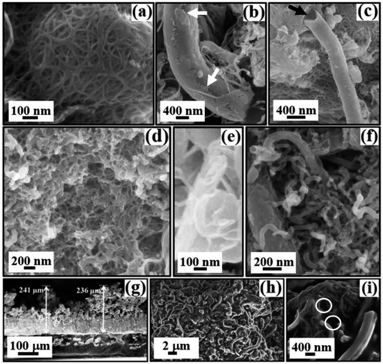 | ||
| Fig. 12 SEM micrographs of purified (a–c), functionalized (d–f) and coated (g–i) samples. The unfused edges and open ends of the CNS are marked by arrows in (b) and (c), respectively. A cross-sectional view of the coated film on the Al substrate is shown in (g) with the thickness marked. The cavities formed on the coated film are shown by circles in (i). | ||
Direct evidence of nesting of the CNTs with agglomeration [Fig. 12(a)], signature of CNS with unfused [Fig. 12(b)] and open [Fig. 12(c)] ends (marked by arrows) can be seen in the purified sample. The nesting and agglomeration are due to the σ and π bonds of the carbon atoms, with the σ bonds forming a strong hexagonal carbon network within the rolled graphene sheets, whereas, the π bonds, perpendicular to the surface of the tubes, try to connect the CNTs by weak vdWs interactions.8,9,25,101,102 The SEM investigations after functionalization [Fig. 12(d–f)] display evenly dispersed CNTs [Fig. 12(d)], a direct manifestation of curling and folding of the carbon sheets to form CNS [Fig. 12(e)] and general morphology of the sample [Fig. 12(f)]. The overall uniform distribution of CNTs after functionalization [Fig. 12(d)] is attributed to the attachment of carboxyl functional groups on the surface,82,83 which improve the dispersion and adhesion properties of the tubes.103
The SEM micrographs obtained from the coated films are shown in Fig. 12(g–i). The cross-sectional view [Fig. 12(g)] reveals the thickness of the film, which is approximately 200–250 μm. The SEM images also disclose the presence of interlinked forests [Fig. 12(h and i)] with cavities or pores [Fig. 12(i)] on the surface (marked by circles).
The AFM investigations on the coated films [Fig. 13(a–c)] further support the presence of interlinked CNT forests. We also observe evidence of microcavities1,29 or holes [Fig. 13(a and b)] on the surface. Considering that the optical properties of the blackest coatings will hugely depend on the surface morphology and related light trapping abilities, the presence of these pores or holes will play an important role in trapping light via multipole reflections104 inside the cavities.
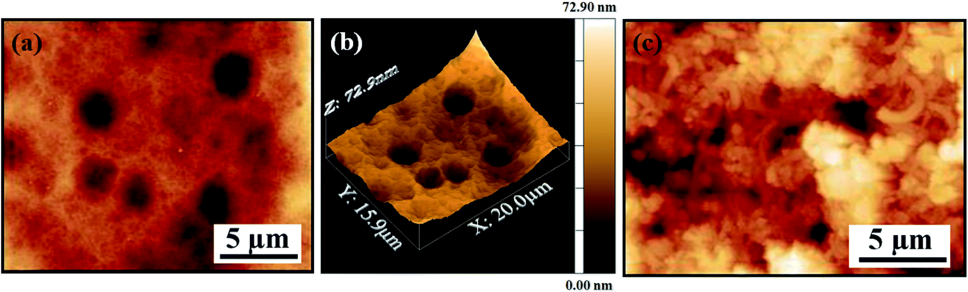 | ||
| Fig. 13 AFM micrographs of the coated film surface. (a and c) Surface morphology with microcavities/holes. (b) 3D projection of the surface shown in (a). | ||
4.6. Spectral reflectance measurement
Hemispherical reflectance measurements are carried out on the spray-coated samples using an integrating sphere attached to the spectrometer. The total reflectance of the coated film before and after subjecting to SEST is presented in Fig. 14(a). Our coated film shows broadband reflectance in the range of 400–2500 nm [Fig. 14(a)]. For the spectral band in the range of 500–1500 nm, an almost uniform variation in reflectance is observed with a minimum value of 2.3%. Fig. 14(a) also shows the reflectance spectra acquired after performing SEST, namely humidity, thermal shock, thermal vacuum and thermal storage. As can be seen in Fig. 14(a), the reflectance spectrum obtained after each SEST exhibits identical behavior as that of the coated film, which clearly demonstrates the stability of the film. Fig. 14(b) shows the plot of the standard deviation of the mean reflectance values obtained from the film after performing each SEST with respect to the value before the SEST (spectral range of 500–1500 nm). It is clearly evident [Fig. 14(b)] that the variation of the mean reflectance values is very small and within the error limit. The percentage deviation is within 0.4 to 1.6, with the thermal shock test giving the lowest variation and the humidity test showing the highest.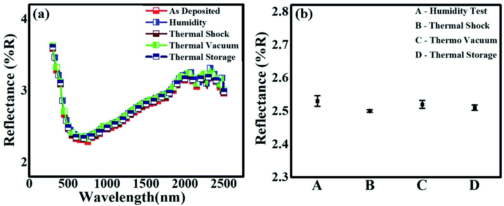 | ||
| Fig. 14 (a) Optical reflectance studies on the as-prepared coated film and after subjected to various SEST. (b) Standard deviation of the mean reflectance values after performing SEST with respect to the as-prepared film. | ||
In Table 2, one can again see that the average reflectance (%) did not change after performing SEST. Several earlier reports on broadband absorption observed in vertically aligned CNT forests were attributed to the formation of compound materials made up of individual nanotubes comprised of different chirality, bandgaps, number of layers, etc.1,25,29 Here, the trapping of light and multiple reflections happening within the cavities and in the nanotubes and nanoscrolls would contribute significantly to the observed low reflectance.
| Test | Tests conditions | Average reflectance (500–1500 nm) (%) | Deviation in reflectance w.r.t. (*) (%) |
|---|---|---|---|
| As-prepared sample (*) | — | 2.49 | — |
| Humidity | 95% relative humidity, 50 °C | 2.53 | 1.6 |
| Thermal shock | −30 °C to +70 °C, 500 cycles | 2.50 | 0.4 |
| Thermal storage | −50 °C to +80 °C, 10 cycles, 2 h dwell time | 2.52 | 0.8 |
| Thermal vacuum cycling | −50 °C to +80 °C, 2 h dwell time, 1 × 10⁻⁵ mbar, 5 cycles | 2.51 | 1.2 |
Post-growth processing of the CNT bundles and site densification105–107 are necessary to achieve the desired property of the CNT-based films. Purification of the as-prepared SWCNTs by chemical oxidation is important to remove the catalyst and carbonaceous contaminants from the bundle network, which in the process, will also modify the CNT structures including cutting and opening them up. The functionalization process is carried out to enhance the solvation properties of the purified CNTs,103 which are usually in the form of bundles and ropes because of interfacial interaction, intrinsic vdWs force, and high aspect ratio.102 Chemical functionalization involves covalent attachment of chemical groups through reactions onto the π-conjugated skeleton of the CNTs by forming a covalent linkage between the functional entities and the carbon skeleton of the tubes.74,103 Furthermore, direct covalent sidewall functionalization with carboxyl groups is associated with a change in hybridization from sp2 to sp3,81–83 whereas indirect covalent functionalization is due to the chemical transformation of the carboxyl groups at the open ends and holes in the sidewalls of the CNT surfaces. In the covalent functionalization process, the CNT structures are further destroyed, resulting in significant changes in their physical properties.9,14,74,101,102,108 In addition to parameters such as diameter, length, and orientation of the tubes, densification also plays a major role in altering the physical properties of the film. Stray light control application requires the successful fabrication of a stable film, which can be achieved using a highly volatile solvent such as acetone associated with a polymer binder. This makes the CNTs come in close contact due to the capillary coalescence effect and creates a random porous network of dense CNT forests.107 We grew solvent-binder wetted layer-by-layer stacking of random forests of CNT–CNS composite films via a simple spray coating technique, where evaporation of the localized solvent caused the CNTs and CNS to come close to each other due to capillary forces, giving rise to a porous mesh-like network.107 Capillary-induced densification can lead to large size pores depending on the choice of solvent.107 The presence of macro-pores with diameters up to a few microns observed on our film surface [SEM and AFM images] can be related to the volatility of the solvent, capillary forces, and the transport of the colloidal particles.107,109 These macro-pores play a vital role in the observed low reflectance value by efficiently trapping the incident light. It has been shown that the refractive index, n, remains almost constant for a densified film compared to the pristine sample106 and densification can reduce the film thickness by approximately 50% to obtain a similar transmittance.106 However, all these features were discussed for wavelengths up to 600 nm, which is much lower than our experimental range to draw any comparison. Ab initio and tight-binding calculations showed that CNS, CNTs, and monolayer amorphous carbon sheets display similar absorption trends with respect to energy with a variation only in the intensity values.110 In the UV-visible range, CNS exhibit a higher absorbance owing to their large curvature compared to CNTs and amorphous carbon sheets. In the spectral range of approximately 300 nm (∼4.13 eV) to 800 nm (∼1.55 eV), the absorbance of CNS is almost twice that of CNTs and amorphous carbon layers, while their reflectivity remains mostly constant.110 The calculated reflectivity and refractive index curves also reveal an identical spectral nature for CNS, CNTs and the carbon sheets in the UV-visible-IR range with a major part of the incident light being absorbed between 1240 nm (1 eV) and 310 nm (4 eV).110 The spectral behavior of our reflectance data appears to be in good agreement with the theoretically predicted results.110 This illustrates the potential of these easily synthesized curved graphene composites, obtained via microstructural changes during processing, as candidates for stray light control and optoelectronics applications.110
4.7. Adhesion test
Adhesion is an important physical property, which is an indicator of proper bonding between the coated film and the substrate. For a coated film to fulfil its function, it should adhere to the substrate properly. Thus, we studied the stability of the films using the ‘Scotch tape method’, which is a commonly used technique to assess the adhesion of CNT coatings with the substrate surface. Fig. 15 shows the sequence of the snapshots carried out on the coated film samples in our case. As can be seen [Fig. 15], the film is gently pressed using normal Scotch tape on the surface.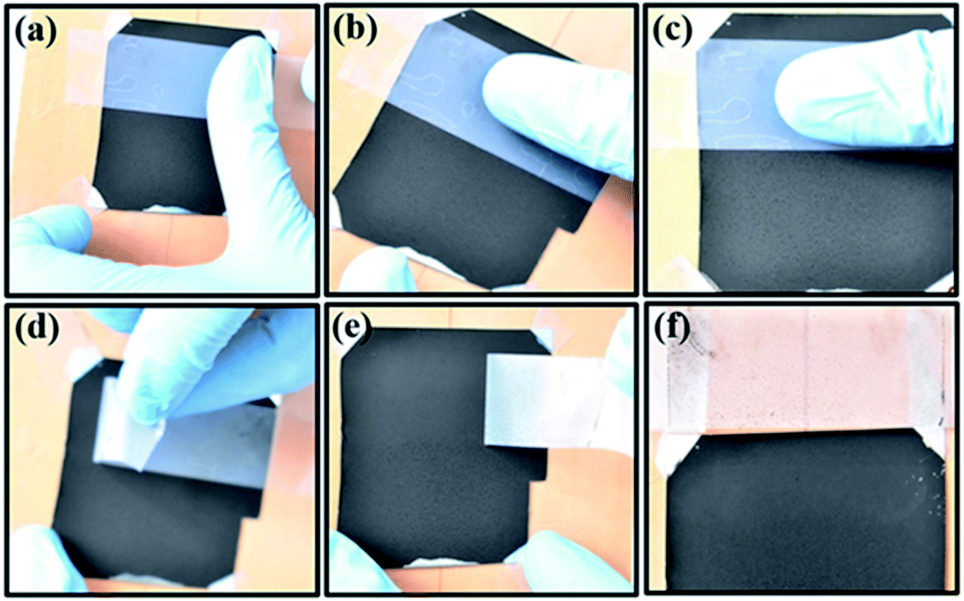 | ||
| Fig. 15 Sequential depiction of the adhesion test performed on the coated film using Scotch tape. | ||
In this case, the film is well adhered to the substrate, and the peeled-off tape does not exhibit any signature of the film coming out with the tape. Rather, only the impression of the loosely bound particles present on the film surface is evident on the tape after removing it. This can be clearly seen in Fig. 15, where the signature of a very small amount of surface particles is only visible on the tape after performing the experiment. The visual analysis [Fig. 15] confirmed the high stability and viability of the CNT, CNS blended film coatings in terms of adhesion with the Al substrate. Well-dispersed CNTs in an Al matrix can pin dislocations driven by the capillary action during solvent evaporation and can form strong chemical bonds with the substrate,111 exhibiting good film stability. A significant contribution would also come from the polyurethane binder due to its physicochemical bonds, high elongation, and tensile strength. The success in the adhesion test allows us to proceed further with the SEST.
4.8. Space environmental simulation tests (SEST)
We carried out elementary space environmental simulation tests (SEST) on these coatings to check their sustainability for space-related applications. Any device that needs to be used in spacecraft has to survive in the space environment, which is entirely different compared to the ground conditions on Earth. CNT coatings have shown great promise in this field for stray light control,1,33 bolometric measurements,1,104 and blackbody sources.1 In this series of experiments, the primary tests include survival of the coatings throughout the launch environment such as vibration, humidity, shock, and extreme temperature. In the humidity test, moisture is allowed to ingress into the surface, which may lead to oxidation, and hence there is a large probability that the properties of the coating will degrade. However, our sample subjected to the humidity test exhibits good stability without any trace of decay in its optical absorptance property. The samples exposed to thermal shock, thermal storage, and thermo-vacuum cycling tests also indicate that the stress and strain due to temperature variations do not affect the films, demonstrating the stability of these coatings under different environmental conditions. Also, the samples do not exhibit any difference visually [Fig. 15] or in the spectral reflectance measurements [Fig. 14 and Table 2] before and after subjecting to the SEST. Details of the SEST are given in Table 2.5. Conclusion
Research on blackest coatings using carbon materials continues to be an evolving field of study. The optical properties of carbon-based coatings need to be tuned according to the requirement and application. The task of making these coatings adequate for specific applications by tailoring the growth process, surface preparation, and modification are technical aspects that are still in progress. Frequent applications of CNT-based thin film coatings are found wherever stray light needs to be controlled, such as coatings for thermal detectors and baffles, various optical components, sensors, space telescopes, and components in spacecraft. We successfully developed a process for the functionalization and preparation of stable thin films of CNTs and CNS via a spray coating technique. The coated films showed promising light reflectance of 2.3–2.8% in the visible and NIR spectral bands in the range of 500–1500 nm. Such a low reflectance value (<3%) of CNTs, CNS blended thin films prepared via a simple spray coating technique has not been reported to date. Herein, we presented our stepwise systematic investigations and analysis to understand the microstructural changes occurring in the as-prepared SWCNTs. The emergence of MWCNTs and CNS is likely to be a processing-induced structural modification of the as-prepared SWCNTs in the sample. Although a plethora of investigations already carried out on MWCNTs demonstrate their highly promising optical absorption properties, studies on CNS are still very limited. Recent theoretical work110 showed that CNS are a better candidate than CNTs in this regard. The microstructural studies carried out on the film surface provide evidence of cavities and pores, which also play an important role in trapping light via multiple reflections. The basic SEST performed according to the standards adopted for the space environment show promising results to consider these CNTs, CNS based coatings as potential high absorber candidates for space-related stray light control applications.Conflicts of interest
There are no conflicts to declare.Acknowledgements
The authors (SS and KB) are thankful to the Director IIST, for the support to carry out the research activity at LEOS. Authors are thankful to NoPo Nanotechnologies Pvt. Ltd for useful initial discussion.References
- K. Mizuno, J. Ishii, H. Kishida, Y. Hayamizu, S. Yasuda, D. N. Futaba, M. Yumura and K. Hata, Proc. Natl. Acad. Sci. U. S. A., 2009, 106, 6044–6047 CrossRef CAS PubMed.
- J. Lehman, C. Yung, N. Tomlin, D. Conklin and M. Stephens, Appl. Phys. Rev., 2018, 5, 011103 Search PubMed.
- J. H. Lehman, C. Engtrakul, T. Gennett and A. C. Dillon, Appl. Opt., 2005, 44, 483–488 CrossRef CAS PubMed.
- J. Lehman, A. Sanders, L. Hanssen, B. Wilthan, J. Zeng and C. Jensen, Nano Lett., 2010, 10, 3261–3266 CrossRef CAS PubMed.
- C. J. Chunnilall, J. H. Lehman, E. Theocharous and A. Sanders, Carbon, 2012, 50, 5348–5350 CrossRef CAS.
- M. A. Quijada, J. G. Hagopian, S. Getty, R. E. Kinzer Jr and E. J. Wollack, in Cryogenic Optical Systems and Instruments XIII, ed. J. B. Heaney and E. T. Kvamme, 2011, vol. 8150, p. 815002 Search PubMed.
- V. J. Gokhale, O. A. Shenderova, G. E. McGuire and M. Rais-Zadeh, J. Microelectromech. Syst., 2014, 23, 191–196 CAS.
- S. Iijima, Nature, 1991, 354, 56–58 CrossRef CAS.
- A. Aqel, K. M. M. A. El-Nour, R. A. A. Ammar and A. Al-Warthan, Arabian J. Chem., 2012, 5, 1–23 CrossRef CAS.
- M. S. Dresselhaus, G. dresselhaus and P. C. Eklund, Science of Fullerenes and Carbon Nanotubes, Academic press, 1996, ISBN: 9780080540771, 0122218205 Search PubMed.
- J. C. Charlier, X. Blase and S. Roche, Rev. Mod. Phys., 2007, 79, 677–732 CrossRef CAS.
- H. Hu, P. Bhowmik, B. Zhao, M. . Hamon, M. . Itkis and R. . Haddon, Chem. Phys. Lett., 2001, 345, 25–28 CrossRef CAS.
- H. Kuzmany, A. Kukovecz, F. Simon, M. Holzweber, C. Kramberger and T. Pichler, 2004, 141, 113–122.
- A. Gromov, S. Dittmer, J. Svensson, O. A. Nerushev, S. A. Perez-García, L. Licea-Jiménez, R. Rychwalski and E. E. B. Campbell, J. Mater. Chem., 2005, 15, 3334 RSC.
- W.-S. Chae, M.-J. An, S.-W. Lee, M.-S. Son, K.-H. Yoo and Y.-R. Kim, J. Phys. Chem. B, 2006, 110, 6447–6450 CrossRef CAS PubMed.
- E. A. Taft and H. R. Philipp, Phys. Rev., 1965, 138, A197–A202 CrossRef.
- H. Servín, M. Peña, H. Sobral and M. González, J. Phys.: Conf. Ser., 2017, 792, 012095 CrossRef.
- Y. S. Touloukian, R. W. Powell, C. Y. Ho and P. G. Klemens, Thermal conductivity – Metallic elements and alloys, 1970, vol. 1 Search PubMed.
- J. Q. Xi, M. F. Schubert, J. K. Kim, E. F. Schubert, M. Chen, S. Y. Lin, W. Liu and J. A. Smart, Nat. Photonics, 2007, 1, 176–179 CrossRef CAS.
- C. Lee, S. Y. Bae, S. Mobasser and H. Manohara, Nano Lett., 2005, 5, 2438–2442 CrossRef CAS PubMed.
- A. Cao, X. Zhang, C. Xu, B. Wei and D. Wu, Sol. Energy Mater. Sol. Cells, 2002, 70, 481–486 CrossRef CAS.
- J. H. Lehman, R. Deshpande, P. Rice, B. To and A. C. Dillon, Infrared Phys. Technol., 2006, 47, 246–250 CrossRef CAS.
- E. Theocharous, R. Deshpande, A. C. Dillon and J. Lehman, Appl. Opt., 2006, 45, 1093–1097 CrossRef CAS PubMed.
- Y. Ma, B. Wang, Y. Wu, Y. Huang and Y. Chen, Carbon, 2011, 49, 4098–4110 CrossRef CAS.
- K. Hata, D. N. Futaba, K. Mizuno, T. Namai, M. Yumura and S. Iijima, Science, 2004, 306, 1362–1364 CrossRef CAS PubMed.
- F. Wang, G. Dukovic, L. E. Brus and T. F. Heinz, Science, 2005, 308, 838–841 CrossRef CAS PubMed.
- S. Maruyama, E. Einarsson, Y. Murakami and T. Edamura, Chem. Phys. Lett., 2005, 403, 320–323 CrossRef CAS.
- A. J. Hart and A. H. Slocum, J. Phys. Chem. B, 2006, 110, 8250–8257 CrossRef CAS PubMed.
- Z.-P. Yang, L. Ci, J. A. Bur, S.-Y. Lin and P. M. Ajayan, Nano Lett., 2008, 8, 446–451 CrossRef CAS PubMed.
- Z. P. Yang, M. L. Hsieh, J. A. Bur, L. Ci, L. M. Hanssen, B. Wilthan, P. M. Ajayan and S. Y. Lin, Appl. Opt., 2011, 50, 1850–1855 CrossRef CAS PubMed.
- J. Zhu, Z. Yu, G. F. Burkhart, C. M. Hsu, S. T. Connor, Y. Xu, Q. Wang, M. McGehee, S. Fan and Y. Cui, Nano Lett., 2009, 9, 279–282 CrossRef CAS PubMed.
- M. D. Kelzenberg, S. W. Boettcher, J. A. Petykiewicz, D. B. Turner-Evans, M. C. Putnam, E. L. Warren, J. M. Spurgeon, R. M. Briggs, N. S. Lewis and H. A. Atwater, Nat. Mater., 2010, 9, 239–244 CrossRef CAS PubMed.
- J. G. Hagopian, S. A. Getty, M. Quijada, J. Tveekrem, R. Shiri, P. Roman, J. Butler, G. Georgiev, J. Livas, C. Hunt, A. Maldonado, S. Talapatra, X. Zhang, S. J. Papadakis, A. H. Monica and D. Deglau, in Carbon Nanotubes, Graphene, and Associated Devices III, ed. D. Pribat, Y.-H. Lee and M. Razeghi, 2010, vol. 7761, p. 77610F Search PubMed.
- H. W. Zhu, Science, 2002, 296, 884–886 CrossRef CAS PubMed.
- N. A. Tomlin, A. E. Curtin, M. White and J. H. Lehman, Carbon, 2014, 74, 329–332 CrossRef CAS.
- H. Shi, J. G. Ok, H. Won Baac and L. Jay Guo, Appl. Phys. Lett., 2011, 99, 211103 CrossRef.
- T. Saleh, M. V. Moghaddam, M. S. Mohamed Ali, M. Dahmardeh, C. A. Foell, A. Nojeh and K. Takahata, Appl. Phys. Lett., 2012, 101, 061913 CrossRef.
- B. D. Wood, J. S. Dyer, V. A. Thurgood, N. A. Tomlin, J. H. Lehman and T.-C. Shen, J. Appl. Phys., 2015, 118, 013106 CrossRef.
- I. B. Dogru, M. B. Durukan, O. Turel and H. E. Unalan, Prog. Nat. Sci.: Mater. Int., 2016, 26, 232–236 CrossRef CAS.
- R. Kavian, A. Vicenzo and M. Bestetti, J. Mater. Sci., 2011, 46, 1487–1493 CrossRef CAS.
- J. J. Butler, G. T. Georgiev, J. L. Tveekrem, M. Quijada, S. Getty and J. G. Hagopian, in Earth Observing Missions and Sensors: Development, Implementation, and Characterization, ed. X. Xiong, C. Kim and H. Shimoda, 2010, vol. 7862, p. 78620D Search PubMed.
- A. Venkataraman, E. V. Amadi, Y. Chen and C. Papadopoulos, Nanoscale Res. Lett., 2019, 14, 220 CrossRef PubMed.
- R. C. Tenent, T. M. Barnes, J. D. Bergeson, A. J. Ferguson, B. To, L. M. Gedvilas, M. J. Heben and J. L. Blackburn, Adv. Mater., 2009, 21, 3210–3216 CrossRef CAS.
- T. S. Li, M. F. Lin, S. C. Chang and H. C. Chung, Phys. Chem. Chem. Phys., 2011, 13, 6138 RSC.
- G. Carotenuto, A. Longo, S. De Nicola, C. Camerlingo and L. Nicolais, Nanoscale Res. Lett., 2013, 8, 403 CrossRef PubMed.
- S. F. Braga, V. R. Coluci, S. B. Legoas, R. Giro, D. S. Galvão and R. H. Baughman, Nano Lett., 2004, 4, 881–884 CrossRef CAS.
- H. Liu, T. Le, L. Zhang and M. Xu, J. Mater. Sci.: Mater. Electron., 2018, 29, 18891–18904 CrossRef CAS.
- X. Xie, L. Ju, X. Feng, Y. Sun, R. Zhou, K. Liu, S. Fan, Q. Li and K. Jiang, Nano Lett., 2009, 9, 2565–2570 CrossRef CAS PubMed.
- J. Zheng, H. Liu, B. Wu, Y. Guo, T. Wu, G. Yu, Y. Liu and D. Zhu, Adv. Mater., 2011, 23, 2460–2463 CrossRef CAS PubMed.
- D. Xia, Q. Xue, J. Xie, H. Chen, C. Lv, F. Besenbacher and M. Dong, Small, 2010, 6, 2010–2019 CrossRef CAS PubMed.
- B. Tang, Z. Xiong, X. Yun and X. Wang, Nanoscale, 2018, 10, 4113–4122 RSC.
- B. Sajadi, S. van Hemert, B. Arash, P. Belardinelli, P. G. Steeneken and F. Alijani, Carbon, 2018, 139, 334–341 CrossRef CAS.
- D. B. Zhang, E. Akatyeva and T. Dumitric, Phys. Rev. Lett., 2011, 106, 3–6 Search PubMed.
- N. G. Chopra, L. X. Benedict, V. H. Crespi, M. L. Cohen, S. G. Louie and A. Zettl, Nature, 1995, 377, 135–138 CrossRef CAS.
- X. Chen, C. Yi and C. Ke, Appl. Phys. Lett., 2015, 106, 2–7 Search PubMed.
- I. Nikiforov, E. Dontsova, R. D. James and T. Dumitrică, Phys. Rev. B: Condens. Matter Mater. Phys., 2014, 89, 1–13 CrossRef.
- D. W. Brenner, O. A. Shenderova, J. A. Harrison, S. J. Stuart, B. Ni and S. B. Sinnott, J. Phys.: Condens. Matter, 2002, 14, 783–802 CrossRef CAS.
- Q. Lu, M. Arroyo and R. Huang, J. Phys. D: Appl. Phys., 2009, 42, 102002 CrossRef.
- P. Koskinen and O. O. Kit, Phys. Rev. B: Condens. Matter Mater. Phys., 2010, 82, 235420 CrossRef.
- K. N. Kudin, G. E. Scuseria and B. I. Yakobson, Phys. Rev. B: Condens. Matter Mater. Phys., 2001, 64, 235406 CrossRef.
- Q. Wang, Phys. Lett. A, 2010, 374, 1180–1183 CrossRef CAS.
- R. Nicklow, N. Wakabayashi and H. G. Smith, Phys. Rev. B: Solid State, 1972, 5, 4951–4962 CrossRef.
- M. J. Bronikowski, P. A. Willis, D. T. Colbert, K. A. Smith and R. E. Smalley, J. Vac. Sci. Technol., A, 2001, 19, 1800–1805 CrossRef CAS.
- V. S. Gangoli, M. A. Godwin, G. Reddy, R. K. Bradley and A. R. Barron, C, 2019, 5, 65 Search PubMed.
- C. C. Ciobotaru, C. M. Damian and H. Iovu, Sci. Bull. - Univ. "Politeh." Bucharest, Ser. B, 2013, 75, 55–66 CAS.
- O. A. Gurova, V. E. Arhipov, V. O. Koroteev, T. Y. Guselnikova, I. P. Asanov, O. V. Sedelnikova and A. V. Okotrub, Phys. Status Solidi, 2019, 256, 1800742 CrossRef.
- A. Suri and K. S. Coleman, Carbon, 2011, 49, 3031–3038 CrossRef CAS.
- J.-M. Moon, K. H. An, Y. H. Lee, Y. S. Park, D. J. Bae and G.-S. Park, J. Phys. Chem. B, 2001, 105, 5677–5681 CrossRef CAS.
- A. Misra, P. K. Tyagi, M. K. Singh and D. S. Misra, Diamond Relat. Mater., 2006, 15, 385–388 CrossRef CAS.
- G. Q. Yu, S. H. Lee and J. J. Lee, Diamond Relat. Mater., 2002, 11, 1633–1637 CrossRef CAS.
- M. M. Stylianakis, J. A. Mikroyannidis and E. Kymakis, Sol. Energy Mater. Sol. Cells, 2010, 94, 267–274 CrossRef CAS.
- E. B. Barros, A. G. S. Filho, V. Lemos, J. M. Filho, S. B. Fagan, M. H. Herbst, J. M. Rosolen, C. A. Luengo and J. G. Huber, Carbon, 2005, 43, 2495–2500 CrossRef CAS.
- Q. M. Li and M. X. Shi, Proc. R. Soc. A, 2008, 464, 1941–1953 CrossRef CAS.
- M. Burghard, Surf. Sci. Rep., 2005, 58, 1–109 CAS.
- D. Roy, E. Angeles-Tactay, R. J. C. Brown, S. J. Spencer, T. Fry, T. A. Dunton, T. Young and M. J. T. Milton, Chem. Phys. Lett., 2008, 465, 254–257 CrossRef CAS.
- D. Roy, M. Chhowalla, H. Wang, N. Sano, I. Alexandrou, T. W. Clyne and G. A. J. Amaratunga, Chem. Phys. Lett., 2003, 373, 52–56 CrossRef CAS.
- D. Roy, M. Chhowalla, N. Hellgren, T. W. Clyne and G. A. J. Amaratunga, Phys. Rev. B: Condens. Matter Mater. Phys., 2004, 70, 1–6 CrossRef.
- J. M. Benoit, J. P. Buisson, O. Chauvet, C. Godon and S. Lefrant, Phys. Rev. B: Condens. Matter Mater. Phys., 2002, 66, 1–4 CrossRef.
- M. S. Dresselhaus, G. Dresselhaus and M. Hofmann, Vib. Spectrosc., 2007, 45, 71–81 CrossRef CAS.
- M. B. Moraes, L. Cividanes and G. Thim, J. Aerosp. Technol. Manage., 2018, 10, e3418 Search PubMed.
- H. M. Park, K. H. Kim, S. H. Lee, D. H. Park, Y. K. Hong and J. Joo, Colloids Surf., A, 2008, 313–314, 72–76 CrossRef.
- J. L. Bahr, J. Yang, D. V. Kosynkin, M. J. Bronikowski, R. E. Smalley and J. M. Tour, J. Am. Chem. Soc., 2001, 123, 6536–6542 CrossRef CAS PubMed.
- C. A. Mitchell, J. L. Bahr, S. Arepalli, J. M. Tour and R. Krishnamoorti, Macromolecules, 2002, 35, 8825–8830 CrossRef CAS.
- V. A. da Silva and M. C. Rezende, Mater. Res., 2018, 21(5), e20170977 Search PubMed.
- R. Siddheswaran, D. Manikandan, R. E. Avila, C. E. Jeyanthi and R. V. Mangalaraja, Fullerenes, Nanotubes, Carbon Nanostruct., 2015, 23, 392–398 CrossRef CAS.
- A. Martinez-Hernandez, C. Velasco-Santos and V. Castano, Curr. Nanosci., 2010, 6, 12–39 CrossRef CAS.
- P. Liu, Eur. Polym. J., 2005, 41, 2693–2703 CrossRef CAS.
- P. N. H. Nakashima, in Encyclopedia of Aluminum and Its Alloys, CRC Press, Boca Raton, 2019 Search PubMed.
- B. Zheng, Z. Xu and C. Gao, Nanoscale, 2016, 8, 1413–1420 RSC.
- D. V. Kosynkin, A. L. Higginbotham, A. Sinitskii, J. R. Lomeda, A. Dimiev, B. K. Price and J. M. Tour, Nature, 2009, 458, 872–876 CrossRef CAS PubMed.
- L. Jiao, L. Zhang, X. Wang, G. Diankov and H. Dai, Nature, 2009, 458, 877–880 CrossRef CAS PubMed.
- A. L. Elias, A. R. Botello-Méndez, D. Meneses-Rodríguez, V. J. González, D. Ramírez-González, L. Ci, E. Muñoz-Sandoval, P. M. Ajayan, H. Terrones and M. Terrones, Nano Lett., 2010, 10, 366–372 CrossRef CAS PubMed.
- U. K. Parashar, S. Bhandari, R. K. Srivastava, D. Jariwala and A. Srivastava, Nanoscale, 2011, 3, 3876–3882 RSC.
- A. G. Cano-ma, F. J. Rodríguez-macı, J. Campos-delgado, C. G. Espinosa-gonza, D. Ramírez-gonza, D. A. Cullen, D. J. Smith, M. Terrones and Y. I. Vega-cantu, Nano Lett., 2009, 9, 1527–1533 CrossRef PubMed.
- L. Xie, H. Wang, C. Jin, X. Wang, L. Jiao, K. Suenaga and H. Dai, J. Am. Chem. Soc., 2011, 133, 10394–10397 CrossRef CAS PubMed.
- L. Jiao, X. Wang, G. Diankov, H. Wang and H. Dai, Nat. Nanotechnol., 2010, 5, 321–325 CrossRef CAS PubMed.
- D. Li, M. B. Müller, S. Gilje, R. B. Kaner and G. G. Wallace, Nat. Nanotechnol., 2008, 3, 101–105 CrossRef CAS PubMed.
- H. Jantoljak, J.-P. Salvetat, L. Forró and C. Thomsen, Appl. Phys. A: Mater. Sci. Process., 1998, 67, 113–116 CrossRef CAS.
- M. J. López, A. Rubio, J. A. Alonso, S. Lefrant, K. Méténier and S. Bonnamy, Phys. Rev. Lett., 2002, 89, 2000–2003 Search PubMed.
- K. H. An, K. K. Jeon, J. M. Moon, S. J. Eum, C. W. Yang, G. S. Park, C. Y. Park and Y. H. Lee, Synth. Met., 2004, 140, 1–8 CrossRef CAS.
- J.-C. Charlier, X. Blase and S. Roche, Rev. Mod. Phys., 2007, 79, 677–732 CrossRef CAS.
- Springer Handbook of Nanotechnology, ed. B. Bhushan, Springer Berlin Heidelberg, Berlin, Heidelberg, 2007 Search PubMed.
- K. Balasubramanian and M. Burghard, Small, 2005, 1, 180–192 CrossRef CAS PubMed.
- W. H. Swartz, L. P. Dyrud, S. R. Lorentz, D. L. Wu, W. J. Wiscombe, S. J. Papadakis, P. M. Huang, E. L. Reynolds, A. W. Smith and D. M. Deglau, in International Geoscience and Remote Sensing Symposium (IGARSS), IEEE, 2015, vol. 2015, pp. 5300–5303 Search PubMed.
- J. Lee, D. M. Lee, Y. Jung, J. Park, H. S. Lee, Y. K. Kim, C. R. Park, H. S. Jeong and S. M. Kim, Nat. Commun., 2019, 10, 1–10 CrossRef PubMed.
- G. Drozdov, I. Ostanin, H. Xu, Y. Wang, T. Dumitrică, A. Grebenko, A. P. Tsapenko, Y. Gladush, G. Ermolaev, V. S. Volkov, S. Eibl, U. Rüde and A. G. Nasibulin, J. Appl. Phys., 2020, 128, 184701 CrossRef CAS.
- X. Yu, X. Zhang, J. Zou, Z. Lan, C. Jiang, J. Zhao, D. Zhang, M. Miao and Q. Li, Adv. Mater. Interfaces, 2016, 3, 1–6 Search PubMed.
- P. M. Ajayan and S. Iijima, Nature, 1992, 358, 23 CrossRef.
- M. Majumder, C. Rendall, M. Li, N. Behabtu, J. A. Eukel, R. H. Hauge, H. K. Schmidt and M. Pasquali, Chem. Eng. Sci., 2010, 65, 2000–2008 CrossRef CAS.
- R. M. Tromer, L. C. Felix, L. A. Ribeiro and D. S. Galvao, Phys. E, 2021, 130, 114683 CrossRef CAS.
- F. Cheng, Y. Hu, Z. Lv, G. Chen, B. Yuan, X. Hu and Z. Huang, Composites, Part A, 2020, 135, 105952 CrossRef CAS.
Footnote |
| † Electronic supplementary information (ESI) available. See DOI: 10.1039/d0na01058h |
| This journal is © The Royal Society of Chemistry 2021 |