DOI:
10.1039/D0NA01046D
(Review Article)
Nanoscale Adv., 2021,
3, 1515-1531
Recent progress in two-dimensional materials for terahertz protection
Received
15th December 2020
, Accepted 28th January 2021
First published on 28th January 2021
Abstract
With the wide applications of terahertz (THz) devices in future communication technology, THz protection materials are essential to overcome potential threats. Recently, THz metamaterials (MMs) based on two-dimensional (2D) materials (e.g., graphene, MXenes) have been extensively investigated due to their unique THz response properties. In this review, THz protection theories are briefly presented first, including reflection loss and shielding mechanisms. Then, the research progress of graphene and other 2D material-based THz MMs and intrinsic materials are reviewed. MMs absorbers in the forms of single layer, multiple layers, hybrid and tunable metasurfaces show excellent THz absorbing performance. These studies provide a sufficient theoretical and practical basis for THz protection, and superior properties promised the wide application prospects of 2D MMs. Three-dimensional intrinsic THz absorbing materials based on porous and ordered 2D materials also show exceptional THz protection performance and effectively integrate the advantages of intrinsic properties and the structural characteristics of 2D materials. These special structures can optimize the surface impedance matching and enable multiple THz scatterings and electric transmission loss, which can realize high-efficiency absorption loss and active controllable protection performance in ultra-wide THz wavebands. Finally, the advantages and existing problems of current THz protection materials are summarized, and their possible future development and applications are prospected.
 Jialiang Pan | Jialiang Pan is a PhD candidate at the School of Materials Science and Engineering, Tsinghua University, China. He works as an Engineer (2007-present) at the First Scientific Research Institute of Wuxi, China. His current research interests focus on materials with nanostructures for electromagnetic applications. |
 Haowen Hu | Haowen Hu is a PhD candidate at the School of Materials Science and Engineering, Tsinghua University, China. He received his B.S. degree in Materials Science and Engineering (2015) from Beihang University and his Master's degree in Polymer Materials Science and Engineering (2016) from the University of Manchester. He is currently working on 2D semiconductor materials and micro-nano electronic devices. |
 Zechen Li | Zechen Li is a PhD candidate at the School of Materials Science and Engineering, Tsinghua University, China. He received his B.S. degree from Tsinghua University in 2019. His research interests focus on the synthesis and structural engineering of nanomaterials for photoelectric detection. |
 Hongwei Zhu | Hongwei Zhu is a Professor of School of Materials Science and Engineering, Tsinghua University, China. He received his B.S. degree in Mechanical Engineering (1998) and his PhD degree in Materials Processing Engineering (2003) from Tsinghua University. After postdoctoral studies in Japan and the USA, he began his independent career as a faculty member at Tsinghua University (2008-present). His current research interests involve low-dimensional materials and materials informatics. |
1. Introduction
As most promising waveband for next generation communication (6G) applications, THz waves have attracted extensive attention.1–4 However, due to potential threats of this unknown waveband to human health, electromagnetic interference, information security and military stealth, essential THz protection materials should be fully studied before their large-scale application. To achieve effective reflection loss or transmission shielding of the surplus THz energy, the THz protection materials are mainly THz absorbing and shielding materials. From the point of view of the interaction between electromagnetic (EM) waves and materials, the response mechanism of natural materials is not continuous across the whole spectrum. Within wavebands of hundreds of gigahertz, electrons dominate the response process to EM waves. Moreover, in the infrared to ultraviolet waveband, the EM waves mainly interact with photons of the materials. However, between the two response areas, the 0.1–10 THz band is a “terahertz gap” which lacks material response; therefore, it is an important topic to develop effective THz protection materials.5,6
Two-dimensional (2D) materials such as graphene and MXenes, due to their high conductivity, ultra-thinness, large specific surface area, ultra-light weight, high strength and adjustable electromagnetic response, have shown excellent microwave attenuation performance,7–9 which has encouraged researchers to realize their THz protection abilities.10–13 However, single atomic layered 2D materials cannot absorb the incident THz energy effectively, and simply stacked materials lead to impedance mismatching.14,15 Therefore, in order to make full use of the advantages of 2D materials, it is very important to reasonably design the forms of 2D materials in THz protective materials, such as patterning the resonance units of MM absorbers and forming nanostructured materials.13,16–18 Because MMs have been proved to respond to THz radiation5 and fully absorb microwave energy,19,20 THz MMs have potential to be perfect THz absorbers. MMs are artificial EM dielectric materials, and are usually composed of an MM layer (high-conductivity materials with periodically repeated patterns), a dielectric spacer and a metal ground layer. Electrons resonated in these subwavelength scale unit structures can form THz absorption;21 therefore, the THz response of MMs can be controlled by designing the unit structure and component materials. Similar to traditional metal resonant MMs layers,22–27 coherent and patterned graphene 2D materials applied as MM layers have been widely studied because of their high conductivities and unique EM responses (such as Surface Plasmon Polaritons (SPPs)).17,18,28–30 Otherwise, for the single atomic layer thickness and tunable chemical potential, 2D materials are easy to composite with other materials, and their EM properties can be controlled by external stimuli. Recently, by optimizing the composite structures and active control approaches of MMs, many THz protection MMs with wide response bands and adjustable absorption performance have been designed.20,31,32
In addition to 2D materials-based THz protection MMs, the nanostructured 2D materials are effective THz protection materials in the form of intrinsic loss.10,16,33 The enhanced absorption of nanostructured materials is mainly contributed by their porous structures and long-distance conductive networks. On the one hand, the porous structure ensures proper effective permittivity, which gives a good impedance match to reduce the surface reflection. On the other hand, the cross-linked 2D materials can generate large surface-induced current, so that the THz radiation rapidly decays and turns into heat in the resistance network. Furthermore, by compositing the nanostructured 2D materials with other THz loss materials, the THz response properties would be further regulated to achieve a wider effective waveband and stronger attenuation capability.16
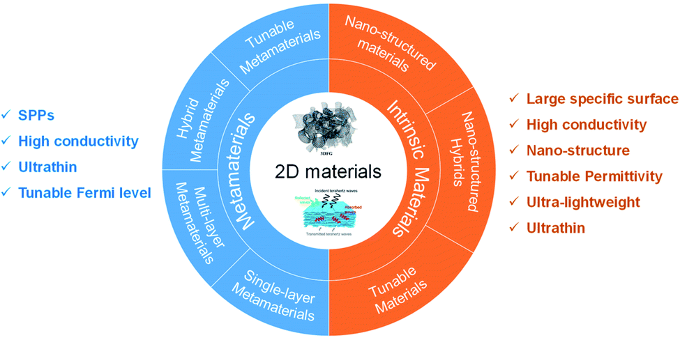
In this Review, we focus on recent progress in THz protection materials based on 2D materials, including THz protection MMs and intrinsic loss materials, as shown in Fig. 1. The 2D materials discussed here are mainly graphene and MXenes, along with phosphorene and other 2D materials. Firstly, the THz protection theories are briefly presented, including reflection loss and shielding mechanisms. Secondly, the research progress of graphene and other 2D materials-based THz protection MMs and intrinsic materials is reviewed. Finally, the advantages and existing problems of current THz protection materials are summarized, and their future development and applications are prospected.
 |
| | Fig. 1 Schematic of THz protection materials based on 2D materials. | |
2. THz protection theory
For different applications, THz protection materials should show different properties. In many cases, the THz protection materials must efficiently absorb THz radiation to reduce the THz echo as much as possible and form reflection loss. In some other cases, the THz transmittance must be strictly low, which can shield the incident THz radiation. The two THz protection theories are briefly presented as follows.
2.1 THz reflection loss
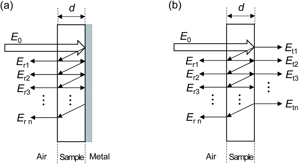
According to electromagnetic transmission theory, a simplified transmission model of THz reflection loss can be established, as shown in Fig. 2a.34,35 The incident THz radiation E0 is transmitted into the absorbing material from the air. The absorbing material is an infinite flat plate with a thickness of d, which is covered with a total reflection metal plate on the back. Er1, Er2 to Ern represent the THz radiation intensity of the first reflection and the second reflection until the n-th reflection, respectively, which are formed after multiple reflections of incident THz through the metal back plate and absorbing material surface. The accumulation of multiple reflection energies forms the total reflection.
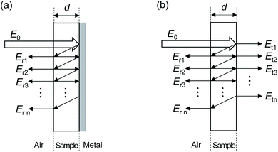 |
| | Fig. 2 Schematic models of (a) THz reflection loss and (b) THz shielding theories. | |
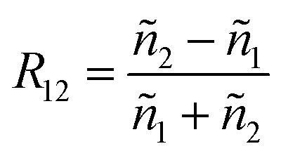
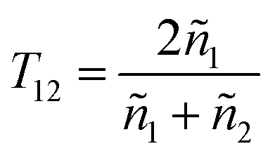
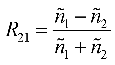
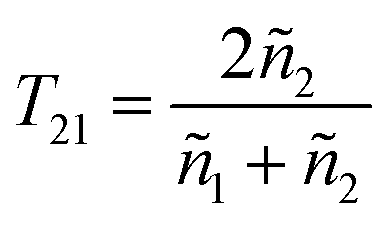
When the THz radiation is normally incident to medium 2 (absorbing material) from medium 1 (air), according to the Fresnel formula, the reflectivity R and transmittance T at the interface can be expressed as follows:35–37
| |  | (1) |
| |  | (2) |
| |  | (3) |
| |  | (4) |
where
ñ1 and
ñ2 are the complex refractive indices of medium 1 and medium 2, respectively. For a lossy medium,
ñ =
n −
κi, where
n and
κ represent the real and imaginary parts of the refractive index, respectively.
The THz wave is attenuated with propagating a certain distance L in the lossy medium, so the intensity of THz radiation EL(ω) can be expressed as follows:35
| | | EL(ω) = E0(ω) × e−iñ(ω)L/c | (5) |
where
c is the speed of light (3 × 10
−8 m s
−1),
ω is the angular frequency (rad s
−1), and
E0(
ω) is the initial THz signal intensity. The propagation loss
Pñ(
ω,
L), which is defined as the power ratio of the THz signal after a propagation length to the initial THz signal, can be expressed as follows:
35
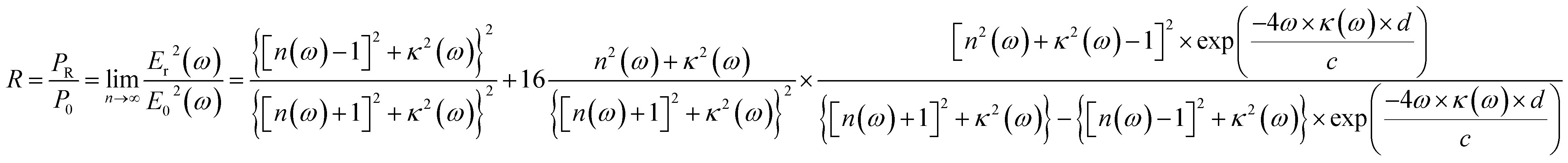
In this case, the total THz energy reflected by the absorbing material can be expressed as follows:34,35
| | | Er2(ω) = Er12(ω) + Er22(ω) + Er32(ω) +, ⋯, + Ern2(ω) = E02(ω) × R122 + E02(ω) × T122 × T212 × Pñ4(ω,L) + E02(ω) × T122 × T212 × R212 × Pñ8(ω,L) +, ⋯, + E02(ω) × T122 × T212 × R212n−4 × Pñ4n−4(ω,L) | (7) |
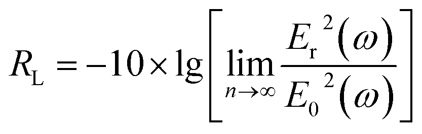
The whole reflectivity (R), which represents the ratio of the total reflected power (PR) to incident power (P0), can be expressed as follows:35–37
| | 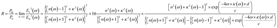 | (8) |
Therefore, the reflection loss (RL) can be written in decibels (dB) as follows:16,34,35
| |  | (9) |
2.2 THz shielding
Similar to the THz reflection loss, a THz shielding model was built with a slight difference, as shown in Fig. 2b.34 The THz shielding material is also an infinite flat plate, but without a metal layer on the back. Therefore, in addition to multiple reflections, there are corresponding THz transmission waves, labeled as Et1, Et2 to Etn.
Accordingly, the total THz transmission of the shielding material can be expressed as the sum of all multiple transmission energies:34,36
| | | Et2(ω) = Et12(ω) + Et22(ω) + Et32(ω) +, ⋯, + Etn2(ω) = E02(ω) × T122 × T212 × Pñ2(ω,L) + E02(ω) × T122 × T212 × R214 × Pñ6(ω,L) + E02(ω) × T122 × T212 × R218 × Pñ10(ω,L) +, ⋯, + E02(ω) × T122 × T212 × R214n−4 × Pñ4n−2(ω,L) | (10) |
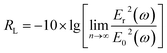
Thus, the whole THz transmittance (T) can be written by the total transmitted power (PT) and the incident power (P0).34,36
| |  | (11) |
Therefore, the electromagnetic shielding effectiveness (EMI SE) can be written in dB as follows:16,34,35
| |  | (12) |
3. Graphene-based THz protection materials
3.1 Graphene-based THz protection MMs
3.1.1 Single-layer graphene MMs.
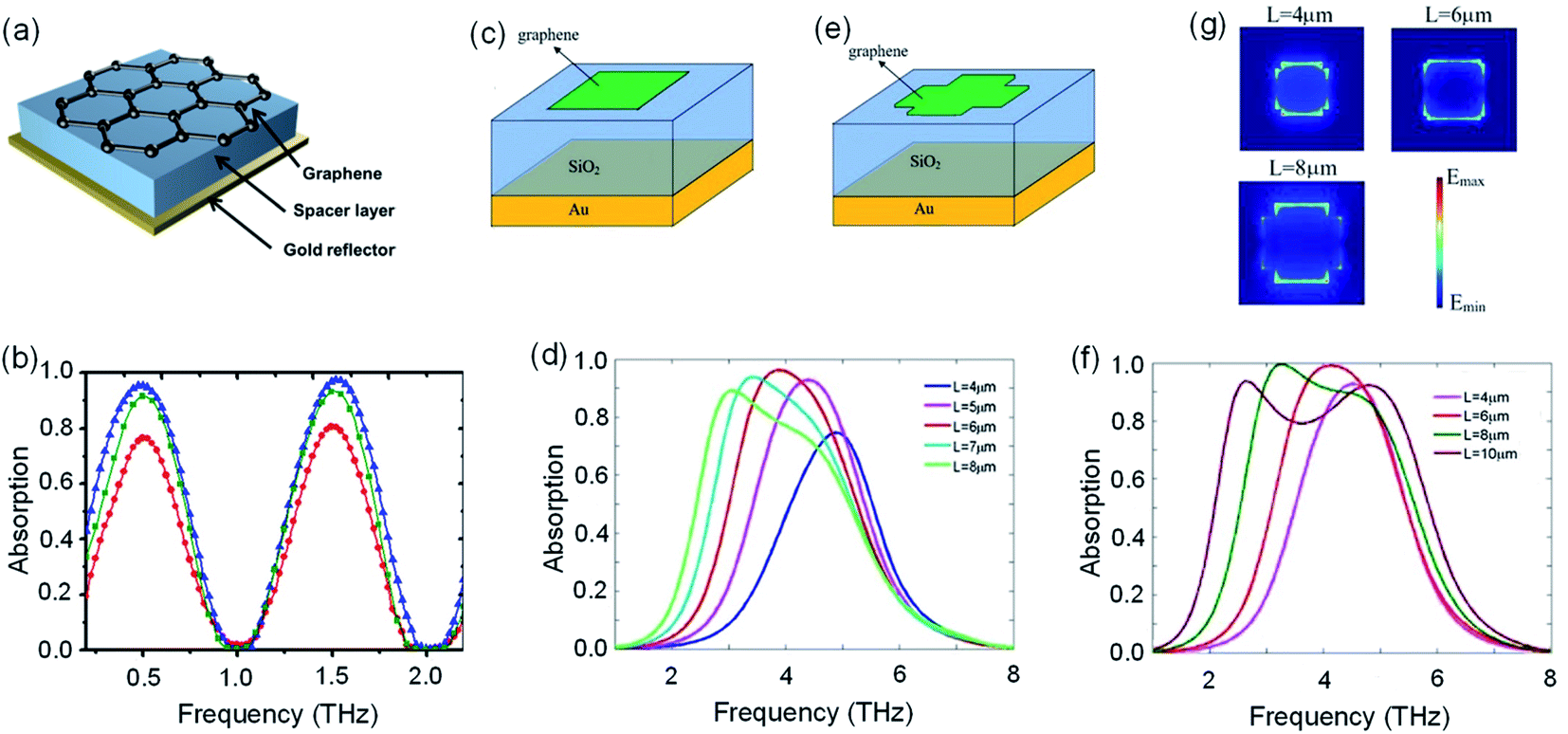
Because of the obvious SPPs in the THz band,30 graphene has been widely studied for THz protection.38–54 However, atomic monolayer graphene is almost transparent to THz waves; thus, the overall intrinsic absorption of monolayer graphene is highly limited.14,15 Therefore, originating from the SPPs effect, well-designed continuous or patterned graphene in the MMs layer can generate collective oscillation of the charge density and light on the interface between graphene and its surroundings, which is beneficial to effective THz absorption and protection.39 The THz response of continuous films was extensively studied, which is promising for further application in THz protection.17,43,55,56 By using polymethyl methacrylate (PMMA), Min et al.56 transferred a continuous 2D graphene sheet grown on nickel to a polymer substrate with a gold-bottomed film. The whole structure built up a Salisbury screen MM, as shown in Fig. 3a, in which the graphene sheet worked as the resistance layer. The conductivity of the graphene sheet could be regulated by chemical doping to match the free space impedance; therefore, the incident THz attenuated directly in the MMs by way of destructive interference. The measured results showed that when the square resistance of the graphene sheet was 689 Ω· □−1, maximum absorptions of 0.95 and 0.97 could be achieved at 0.97 and 1.5 THz (Fig. 3b). In addition, some patterned graphene, such as square,38,57 cross,58–61 disk,60,62 ribbon,63,64 ring39,65,66 and pixel67 shapes, have been designed and simulated for THz absorption. Xiao et al.59 designed rectangular and cross-shaped graphene metasurfaces for THz absorption (Fig. 3c and e). The full-wave simulation showed that both MMs indicated effective absorbing ability, and the effective absorption (absorption above 90%) bandwidth of the cross-shaped MMs could reach 1.13 THz (Fig. 3d and f). Furthermore, generated from the higher real part conductivity of graphene surface and larger propagation loss of the SPPs, the absorbing range in the low-frequency region was broadened. As shown in Fig. 3g, the electric field distribution at the absorption peak revealed that the localization fields on the edges of the patterned graphene were obviously stronger because of the charge accumulation excited by the electric dipole resonances.
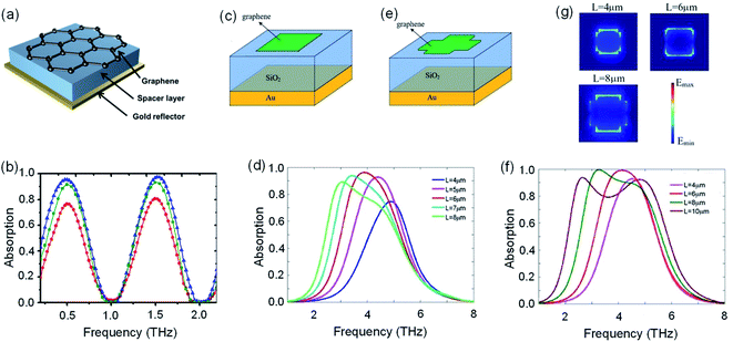 |
| | Fig. 3 (a) Diagram of graphene-based Salisbury screen MMs. (b) THz absorption of the MMs illustrated in (a) with different square resistances (sample A: 1295 Ω □−1 (●), sample B: 817 Ω □−1 (■), and sample C: 689 Ω □−1 (▲)) (reproduced with permission from ref. 56. Copyright 2014 AIP Publishing). (c) Unit cell of MMs with the rectangular array. (d) THz absorption of the MMs illustrated in (c) for various values of length L. (e) Unit cell of MMs with the cross-shaped array. (f) THz absorption of the MMs illustrated in (e) for various values of length L. (g) Electric field distributions of the MMs illustrated in (e) at the absorption peak for different values of L (reproduced with permission from ref. 59. Copyright 2017 The Optical Society). | |
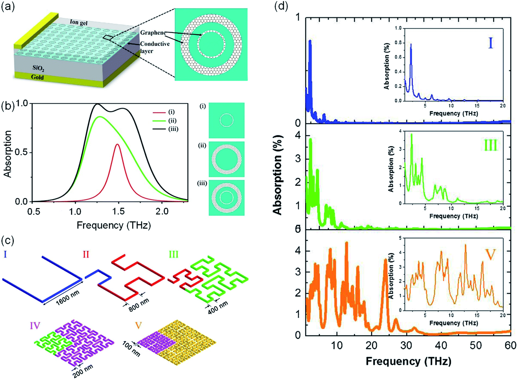
Meanwhile, some complex or composite graphene patterns were proposed to enhance THz absorption39,60,66,68,69 so that the absorbing bandwidth could be broadened by the multiple resonant peaks generated from the multi-structures. Mou et al.66 designed a patterned graphene concentric double rings (GCDR) metasurface to enlarge the absorbing bandwidth by forming plasmonic hybridization between two graphene rings (Fig. 4a). The calculated absorption results shown in Fig. 4b revealed that the MMs with GCDR can effectively absorb THz energy above 90% ranging from 1.18 to 1.64 THz, with two isolated absorption peaks located at 1.26 and 1.54 THz. Meanwhile, the MMs with only inner or outer graphene single rings exhibited single absorption peaks and narrow bandwidths, corresponding to the high-frequency and low-frequency peaks of the GCDR structures. The coupling effect between the two graphene rings obviously enhanced the THz absorption, with stronger dissipating ability and wider bandwidth. Moreover, to further broaden the absorption bandwidth, Wu et al.69 proposed broadband MMs based on the self-affine fractal Hilbert curves, in which the self-affine multi-scale structures could induce different resonant frequencies, and the first five (I–V) iterative levels of the Hilbert curves are shown in Fig. 4c. As shown in Fig. 4d, with the increment of the Hilbert curve level, the responsive absorption bandwidth was clearly broadened for the multiple resonant behaviors, which originated from the self-affine structures.
 |
| | Fig. 4 (a) Schematic of the THz absorber consisting of the GCDR. (b) Simulated absorptions of the proposed GCDR absorber with different graphene patterns (reproduced with permission from ref. 66 Copyright 2018 The Optical Society). (c) Iterative construction of the Hilbert curve for the first five (I–V) levels. (d) Simulated absorptions for graphene Hilbert structures of levels I, III, and V (reproduced with permission from ref. 69 Copyright 2016 American Physical Society). | |
3.1.2 Multi-layer graphene MMs.
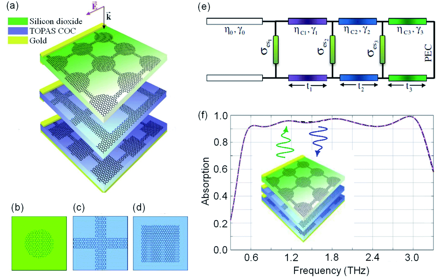
Multi-layer graphene MMs were also commonly introduced to achieve broadband THz protection. The resonant frequencies and coupling effects can be manipulated by designing the graphene patterns of each metasurface to enable the multi-layer graphene MMs to respond to more frequencies and wider THz bandwidths.15,28,70–78 Rahmanzadeh et al.15 designed the three-layer MMs composed of different graphene metasurfaces with square, cross and circle-shaped patterns, respectively. The multi-layer structures and graphene patterns of each layer are shown in Fig. 5a–d. According to the equivalent circuit model, the patterned graphene layers could be simulated as the dispersion complex impedances (Fig. 5e), in which the structural parameters could be theoretically designed for the optimal absorption performance. The THz absorption results of the full-wave simulation shown in Fig. 5f revealed that the multi-layer graphene MMs achieved ultra-wide effective bandwidth, ranging from 0.55 to 3.12 THz. By analyzing the induced electric field, surface current and power loss density of each patterned graphene metasurface, it was clear that the SPPs played a dominant role in the THz dissipation process and formed the physical absorption mechanism of the multi-layer graphene MMs. Meanwhile, the simulation results also verified that the designed structure was omnidirectional and polarization insensitive; therefore, the MMs could effectively protect the device under multi-polarization THz incidences from wide incident angles.
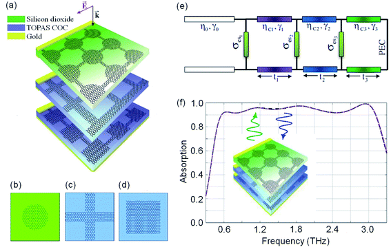 |
| | Fig. 5 (a–d) Structure, (e) transmission line model and (f) simulated absorption of multiple-layer graphene MMs (reproduced with permission from ref. 15 Copyright 2018 The Optical Society). | |
3.1.3 Hybrid graphene MMs.
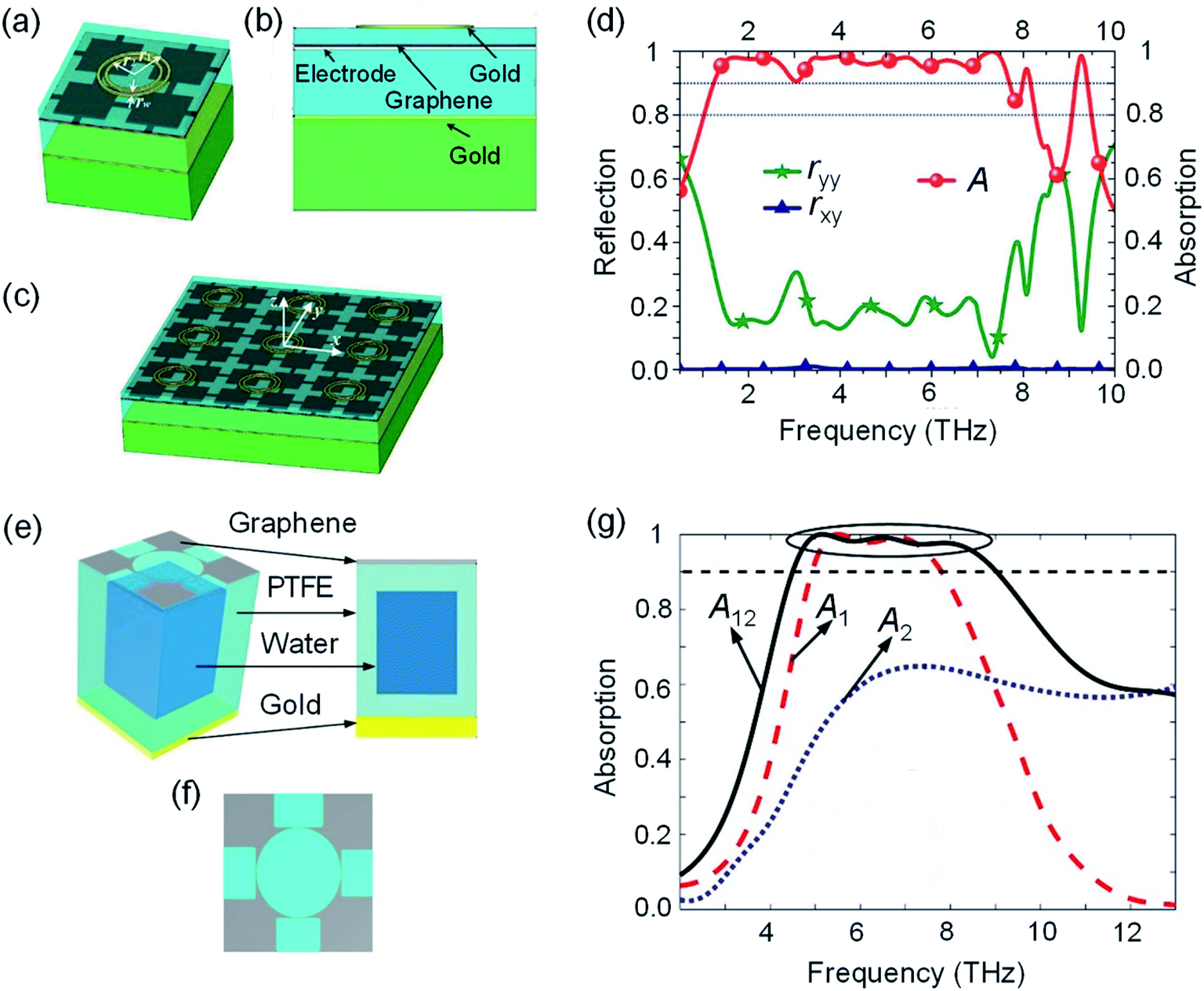
In order to further expand the THz response bandwidth and strengthen the THz absorption capability of THz protection materials, it is also effective to combine graphene with other THz responsive materials, such as metals,18,79–88 Si,89–93 water94 and other materials.95,96 By reasonably designing the meta-structures of each component, the comprehensive advantages of each material can be utilized. Peng et al.85 designed the hybrid MMs based on four graphene fishing net structures and double metal rings (Fig. 6a–c). As the simulated results show in Fig. 6d, the effective absorption bandwidth of the graphene–metal hybrid MMs could reach as high as 6.46 THz (1.24–7.70 THz). Meanwhile, the absorber was insensitive to different polarizations and incident angles of the THz incidence. The ultra-wide effective THz absorption bandwidth of the graphene–metal hybrid MMs was formed by the following three factors: (i) the SPPs of the graphene metasurface were enhanced by the metal metasurface, leading to the enhancement of the confined field. (ii) The resonance coupling of the metal and graphene metasurface could trap the incident THz wave between the two metasurfaces, which could form energy exchange and dissipation. (iii) The multiple THz reflections and their superposition between the metasurface and gold substrate further enhanced the THz absorption. In addition, the absorption bandwidth could be broadened by composing graphene MMs with water by taking advantage of the intrinsic dispersive permittivity of water. Zhang et al.94 designed a graphene–water hybrid MMs THz absorber with an ultra-wide effective waveband, in which water was encapsulated in the polytetrafluoroethylene (PTFT) dielectric material with the patterned graphene metasurface on the top (Fig. 6e and f). The simulated results shown in Fig. 6g present a broad THz effective bandwidth covering 4.52–9.02 THz. It also could be seen that the broadband absorption was superimposed by three absorption peaks, in which two low-frequency absorption peaks were excited by the graphene metasurface, and the high-frequency peak was induced by the water. Moreover, by introducing the filling water, the absorption bandwidth of the hybrid absorber was obviously increased by 57.34% compared to the absorber without water, while the absorption peak of the graphene metasurface was not shifted. Otherwise, the graphene–water MMs absorber was confirmed to be insensitive to the incident angles and polarizations.
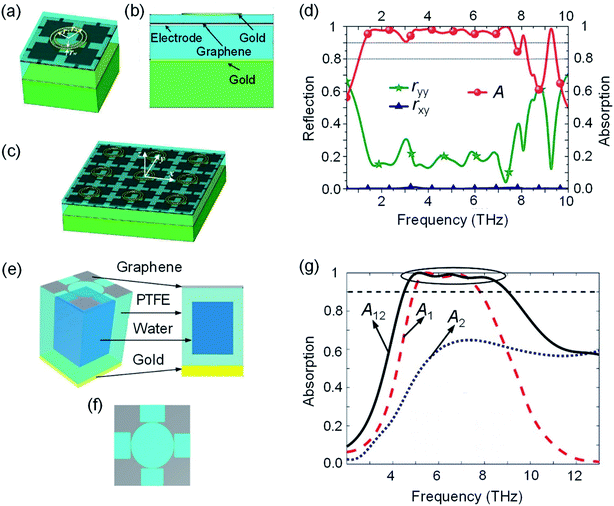 |
| | Fig. 6 (a–c) Schematic view of a graphene–metal MMs THz absorber. (d) Simulated THz absorption and reflection of graphene–metal MMs (reproduced with permission from ref. 85 Copyright 2019 The Royal Society of Chemistry). (e and f) Schematic view of a graphene–water MMs THz absorber. (g) Simulated THz absorption of graphene–water MMs (A12: graphene–water hybrid MMs, A1: A12 MMs without water, A2: A12 MMs without the patterned graphene metasurface) (reproduced with permission from ref. 94 Copyright 2020 Elsevier). | |
3.1.4 Tunable graphene MMs.
Because graphene is a typical 2D semiconductor, its electron mobility and Fermi level can be controlled by external stimulations, such as an electrostatic field,59,90,97–110 magnetic field,111,112 optical pump113 and temperature.83,114 The resonance frequencies of the designed graphene structures can thus be regulated by external stimulation, which can form effective and broadband THz absorption. According to the Kubo formula, the surface conductivity of graphene could be expressed as follows:103| | 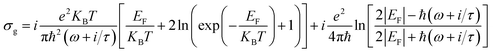 | (13) |
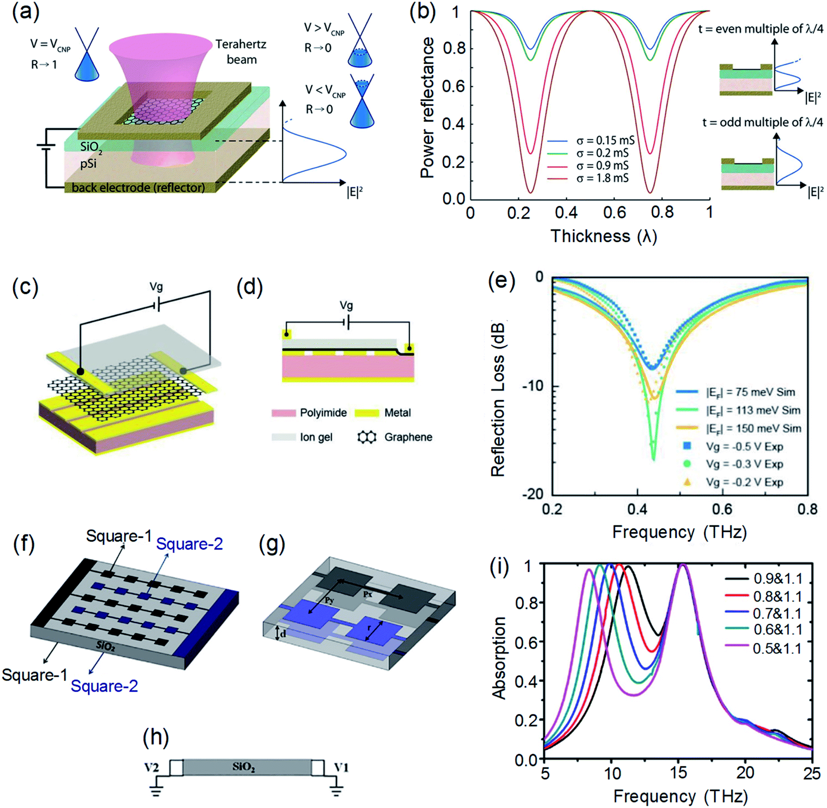
where KB, e, ℏ, τ, T and EF are the Boltzmann constant, electron charge, reduced Planck's constant, relaxation time, temperature and Fermi level, respectively. From the formula, it is obvious that the surface conductivity of graphene can be actively controlled by the Fermi level and temperature. Sensale-Rodriguez et al. designed an extraordinary controllable THz modulator by transferring single-layer graphene onto a SiO2/p-Si substrate (Fig. 7a).110 The carrier concentration and Fermi level in graphene could be tuned when the voltage employed between the graphene and back metal was changed. While the Fermi level was modulated to the Dirac point (V = VCNP), the THz absorption was at its minimum. Moreover, the THz absorption increased as the Fermi level shifted into the valence or conduction band, due to the intraband transition of the available density of states. The calculated power reflectance in Fig. 1b showed that the field intensity in graphene is maximum when the optical thickness of the substrate is an odd-multiple of the THz wavelength, in which obvious absorption swings occurred when the conductivity in graphene was extraordinarily controlled. However, the THz absorption was very low and did not change when the substrate thickness was an even-multiple of the THz wavelength. Furthermore, by integrating the metal grating into chemical vapor deposition (CVD)-grown graphene sheet Salisbury screen MMs, Chen et al.103 realized an electrically tunable hybrid THz MM absorber based on an ion gel/graphene/stripe Al/polyimide (PI)/Al thin film structure (Fig. 7c and d). The Fermi level of the graphene layer could be changed by the external bias voltage, which could lead to controllable THz absorbing ability. The experimental results showed that it is feasible to achieve tunable THz absorption based on graphene grown by CVD with low carrier mobility, and the modulation depth of the THz absorption could reach 25% by applying relatively small bias voltage (−2 to 2 V), as shown in Fig. 7e. Then, the numerical simulations based on transmission line theory and full-wave simulation software also verified the measured results. In addition to graphene nanosheets, some patterned graphene structures were also designed and prepared for tunable THz absorption. Jin et al.104 designed a coherent perfect absorber based on the square patterned graphene structure, which was composed of two alternately arranged graphene MM layers (Fig. 7f–h). The Fermi level of each staggered metastructure could be independently controlled by the applied bias voltage distributed on the side. The numerical simulation results showed that the absorbing frequency peaks can be effectively controlled by changing the applied voltage values, and the absorber presented two independent tunable absorption peaks when the applied voltages of each staggered metastructure were different (Fig. 7i). Moreover, when the absorber was stacked by the metastructures in layers, multiple THz absorption peaks could be formed to achieve an ultra-wide THz absorbing waveband. Although the preparation of tunable patterned graphene MMs is currently difficult, it can also be achieved by template selective etching and some other new methods.101
 |
| | Fig. 7 (a) Schematic structure, operating principle and (b) calculated power reflectance of a graphene THz absorption modulator (reproduced with permission from ref. 110 Copyright 2012 American Chemical Society). (c and d) Schematic view and (e) simulated THz reflection of the tunable MMs THz absorber based on graphene film (reproduced with permission from ref. 103 Copyright 2020 John Wiley and Sons). (f–h) Schematic view and (i) simulated THz absorption of the tunable MMs THz absorber based on patterned graphene (reproduced with permission from ref. 104 Copyright 2019 Elsevier). | |
3.2 Graphene intrinsic THz protection materials
3.2.1 Graphene foams.
As an advanced carbon material with high thermal conductivity, high strength, large specific surface area, optical transparency and adjustable electromagnetic response, graphene has been widely used in radar wave attenuation and showed excellent loss performance;7 therefore, its THz protection applications have attracted much attention.10–12,35 In contrast to the reflection mechanism of traditional metal THz shielding materials, Zdrojek et al.11 prepared flexible THz shielding materials by dispersing graphene nanosheets in a polydimethylsiloxane (PDMS) matrix, whose shielding effect was mainly contributed by absorption. The shielding material showed excellent unit shielding efficiency exceeding 30 dB cm−3 g−1. However, because of their inhomogeneous dispersion and interface mismatch, the THz shielding materials of this type would produce large surface reflections; thus, the maximum absorption hardly reached 80%. Therefore, adjusting the THz characteristics and improving THz attenuation are still challenging.10 In recent years, with the fabrication development of 3D porous materials, such as graphene foams, THz absorbers with conductive networks and large surface areas can be established which can provide excellent impedance matching and THz energy attenuation.7,10,35,115 Huang et al.10 prepared a 3D porous graphene foam with a density of only 0.8 g cm−3 by a solvothermal method (Fig. 8a). The optimal reflection loss of the THz absorber could reach 19 dB at 0.88 THz, and the effective absorbing bandwidth (reflection loss above 10 dB) could cover 95% of the test band (0.1–1.2 THz) under normal conditions, as shown in Fig. 8b. Moreover, when the incident angle was 45°, the effective bandwidth covered the whole test bandwidth, while the optimal reflection loss was 28.6 dB at 0.64 THz (Fig. 8c). It was found that the outstanding THz absorbing ability of 3D graphene foam mainly originates from the porous structure and long distance conductive network. On the one hand, the effective dielectric constant and impedance matching degree can be optimized by designing the porous structures to reduce the surface reflection. On the other hand, the 3D graphene sheets could induce surface currents under the THz radiation so that the incident THz energy would be rapidly decayed in the resistance network by being converted into heat.
 |
| | Fig. 8 (a) Cross-section SEM image of the 3D graphene foams. (b) Reflection loss curves of some graphene foam samples. (c) Reflection loss curves of the T1000 samples with 4 mm thickness at different incident angles (reproduced with permission from ref. 10 Copyright 2018 John Wiley and Sons). (d) SEM image, structural diagram, (e) EDS maps and (f) reflection loss curve of the graphene/Fe3O4 hybrid foams (reproduced with permission from ref. 35 Copyright 2019 American Chemical Society). | |
3.2.2 Graphene hybrid foams.
To further enhance the THz protection properties, 3D graphene foams composited with carbon nanotubes,116 Fe3O4 (ref. 35) and other dielectric/magnetic particles were proposed to perform multiple attenuation mechanisms. Chen et al.35 prepared high-performance graphene/Fe3O4 3D porous electromagnetic protection foams with ultra-lightweight and ultra-wide effective wavebands (Fig. 8d and e). The measured results showed that the 3D foams could achieve an effective absorption waveband covering 3.4 GHz to 2.5 THz, while the average reflection loss reached −38 dB (Fig. 8f). In addition, the 3D composite foams exhibited excellent absorption properties under oblique incidence and different compression strains, while the absorber still maintained a stable absorption ability after 200 repeated compression/release cycles. The addition of magnetic particles further regulated the electromagnetic characteristics of the 3D graphene porous cross-linked structures, which greatly broadened the response waveband and provided a strong technological foundation for active protection materials according to the increasingly complex electromagnetic environments in the future.
3.2.3 Tunable graphene THz protection materials.
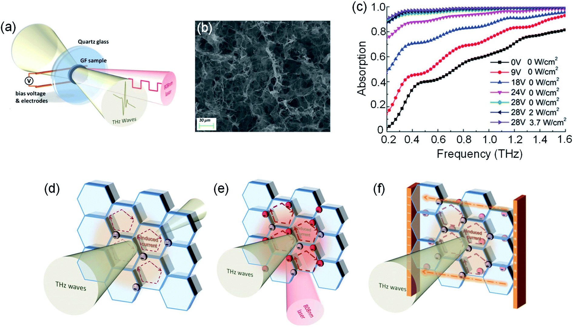
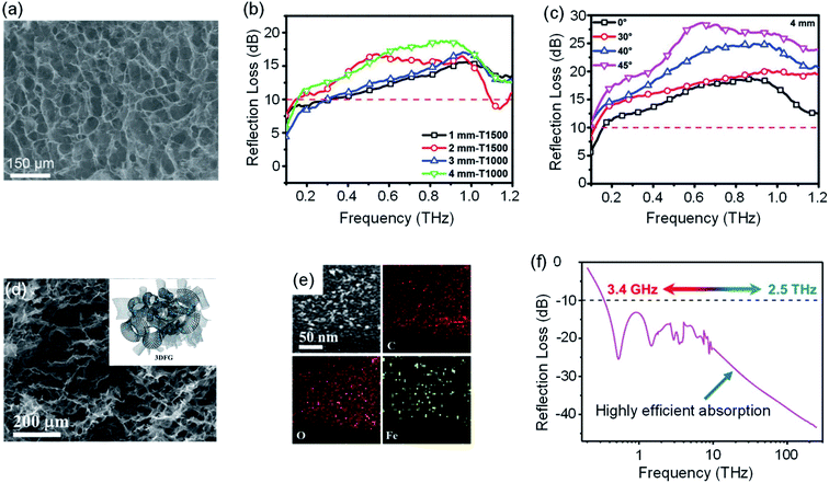
In addition, because the Fermi level and carrier concentration of graphene can be conveniently regulated by some external stimuli, such as electric field and optical radiation, THz absorbing modulation of graphene foams is also available. Xu et al.36 studied the active modulation behaviors of an 800 nm laser and bias electric field on graphene foams, and they realized flexible regulation of THz shielding and absorbing performance. A schematic of the external stimulus control and the microstructures of the graphene foams are shown in Fig. 9a and b. The absorptivity curves shown in Fig. 9c reveal that the THz absorption was strongly related to the frequency when there was no external field, with an absorptivity change from 0.04 at 0.2 THz to 0.8 at 1.6 THz. Furthermore, the absorption increased sharply with the increment of the excitation intensity. The absorptivity changed rapidly from 0.13 to 0.954 at the low frequency of 0.3 THz, while the absorptivity at the high frequency of 1 THz varied from 0.62 to 0.995. The excellent THz absorbing modulation properties can be explained as follows: (i) without external stimulation, the cross-linked graphene networks can be regarded as numerous coupling circuits of resistance, inductance and capacitance; therefore, the time-varying THz field could excite induced currents on the cell wall of graphene. These long-range induced currents attenuated rapidly in the high resistance networks, resulting in sharp decay of the incident THz wave (Fig. 9d). (ii) When the graphene foams were stimulated by a laser or electric field, the nonequilibrium carriers could be generated to raise the Fermi level to a higher conduction band and enhance the THz absorption (Fig. 9e and f). (iii) Fundamentally, because the laser radiation could not penetrate the interior of the graphene foams, the photo-generated carriers could only be generated in the shallow layer of the foams. However, the electric field could pass through the whole graphene foams, resulting in more nonequilibrium carriers on the graphene sheets, which caused a superior regulating effect compared to laser radiation.
 |
| | Fig. 9 (a) Schematic of electrically and optically controlled graphene foams for THz modulation and absorption. (b) SEM image of tunable THz absorbing graphene foams. (c) The absorptivity curves of tunable graphene foams stimulated by different electrical voltages and laser excitations. Schematic of THz wave propagation and interaction with free electrons in the graphene foams (d) without external field excitations, (e) excited by the laser light and (f) excited by the electric field (reproduced with permission from ref. 36 Copyright 2019 John Wiley and Sons). | |
4. Other 2D THz protection materials
4.1 MXene-based intrinsic THz protection materials
In addition to graphene, MXenes have been commonly used as 2D THz protection materials in recent years.13,16,37,117 MXenes are 2D transition-metal carbide and nitride materials with the general formula Mn+1XnTx. MXenes have attracted extensive attention for their unique mechanical, structural, physical and chemical properties, among which the ultra-high conductivity (1500 S cm−1) and hydrophilic surface endow them with excellent electromagnetic response characteristics and controllable structures.9,118,119 2D MXene nanosheets can induce conductance of incident electromagnetic waves between the nanosheets due to their good internal conductivity and particular layer spacing, which has been proved to enhance the electromagnetic absorption effectively.9,120 Furthermore, Jhon et al.121 theoretically confirmed the intrinsic THz response characteristics of MXenes through first principles. Thus, Ma et al.37 prepared ultra-light and compressible THz-absorbing 3D porous MXene/graphene oxide (GO) foams by a solvothermal method (Fig. 10a–c). The absorber combined the advantages of MXenes and GO, forming tunable and ultra-wideband THz absorption properties. MXene/GO foams showed high THz loss efficiency during the whole test range (0.2–2.0 THz) with the maximum reflection loss of 37 dB at 2 THz. Also, when the mass ratio of MXene and GO was 1![[thin space (1/6-em)]](https://www.rsc.org/images/entities/char_2009.gif) :5, the absorber presented the maximum average absorption loss of 30.6 dB. Moreover, after compression was repeated 200 times, the THz absorption performance of the composite foams was almost unchanged (Fig. 10d). Similar to graphene foam structures, 3D porous MXene/GO foams could produce better impedance matching and larger induced current loss, and the introduction of MXenes with high THz response could further improve the THz absorption performance. By utilizing the cross-linking reinforcement of the multivalent metal ions to MXene and GO nanosheets, Lin et al.16 prepared free-standing, lightweight, foldable and highly stable MXene/GO/Zn2+ THz shielding foams by an ion-diffusion-induced gelation method (Fig. 10e). The measured morphology results showed that a small amount of the Zn component was evenly distributed in the homogenous foams, and the nanosheets were tightly packed in the cell walls of the foams (Fig. 10f–h). The unique cross-linked porous structures and moderate conductivity endowed the foams with higher THz shielding ability and lower surface reflection (Fig. 10i). The THz protection test results showed that when the thickness of the 3D foams was only 85 μm, the electromagnetic shielding effectiveness could reach 51 dB, while the reflection loss below −10 dB could cover 0.86–2.0 THz (Fig. 10j and k).
:5, the absorber presented the maximum average absorption loss of 30.6 dB. Moreover, after compression was repeated 200 times, the THz absorption performance of the composite foams was almost unchanged (Fig. 10d). Similar to graphene foam structures, 3D porous MXene/GO foams could produce better impedance matching and larger induced current loss, and the introduction of MXenes with high THz response could further improve the THz absorption performance. By utilizing the cross-linking reinforcement of the multivalent metal ions to MXene and GO nanosheets, Lin et al.16 prepared free-standing, lightweight, foldable and highly stable MXene/GO/Zn2+ THz shielding foams by an ion-diffusion-induced gelation method (Fig. 10e). The measured morphology results showed that a small amount of the Zn component was evenly distributed in the homogenous foams, and the nanosheets were tightly packed in the cell walls of the foams (Fig. 10f–h). The unique cross-linked porous structures and moderate conductivity endowed the foams with higher THz shielding ability and lower surface reflection (Fig. 10i). The THz protection test results showed that when the thickness of the 3D foams was only 85 μm, the electromagnetic shielding effectiveness could reach 51 dB, while the reflection loss below −10 dB could cover 0.86–2.0 THz (Fig. 10j and k).
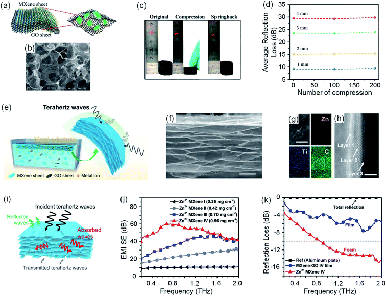 |
| | Fig. 10 (a) Digital images, (b) structural diagram and (c) SEM image of MXene/GO 3D foam. (d) Reflection loss curves of MXene/GO 3D foams with different thicknesses after compression 0, 100 and 200 times (reproduced with permission from ref. 37 Copyright 2019 American Chemical Society). (e) Structural diagram, (f) sectional SEM image, (g) EDS maps, (h) HAADF-STEM image, (i) THz shielding schematic, (j) THz shielding efficiency curves and (k) reflection loss curves of MXene/GO/Zn2+ composite 3D foams (reproduced with permission from ref. 16 Copyright 2020 American Chemical Society). | |
4.2 Tunable MXene-based THz protection materials
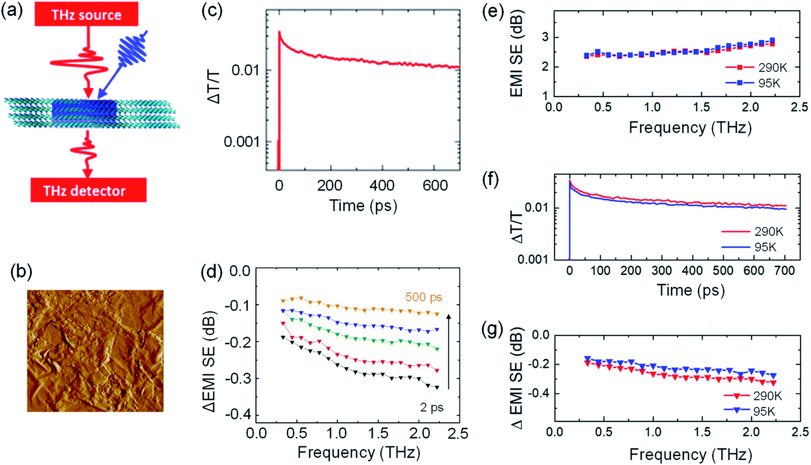
Because the electric conductivity of MXenes can be inhibited by external optical stimulation, it is possible to modulate their THz shielding properties. Therefore, Li et al.117 studied the THz shielding regulation of MXene films stimulated by an ultrafast optical pulse (Fig. 11a). Due to the synergistic effects of THz absorption and reflection, the THz shielding effectiveness per unit thickness of the highly conductive Ti3C2Ty thin film with a thickness of only 25 nm (Fig. 11b) could reach 4 × 10⁵ dB cm−2 g−1, which indicates that the THz shielding effectiveness of a micron-thickness film could reach tens of decibels. After the stimuli of 400 and 800 nm optical pulses, the transient THz transmittance of the MXene film could be enhanced within 2 ps. The THz shielding was suppressed by the photoinduced transient decrease of the real conductivity components which were proportional to the THz absorption, leading to more THz transmission. Additionally, with increasing irradiation time, the influence on the THz transmittance and shielding gradually weakened (Fig. 11c and d). Moreover, the measured results revealed that the THz shielding effectiveness could be reduced within nanoseconds through ultrafast optical pulses ranging from 95 K to room temperature (Fig. 11e–g). Due to these unique properties, MXenes are promising for the dynamic control of THz shielding and detection devices.
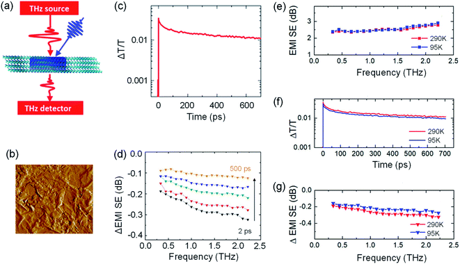 |
| | Fig. 11 (a) THz shielding modulation schematic of the MXene film stimulated by optical radiation. (b) AFM micrograph of a 25 nm-thick Ti3C2Ty film. (c) THz transmittance and (d) shielding effectiveness changes under different optical radiation times. (e) THz shielding effectiveness of the MXene film at 290 and 95 K without external stimuli. (f) THz transmittance changes after excitation with 800 nm and 950 μJ cm−2 laser pulses at 290 and 95 K. (g) THz shielding effectiveness changes 2 ps after photoexcitation at 290 and 95 K with 800 nm and 950 μJ cm−2 pulses (reproduced with permission from ref. 117 Copyright 2020 American Chemical Society). | |
4.3 Other 2D THz protection materials
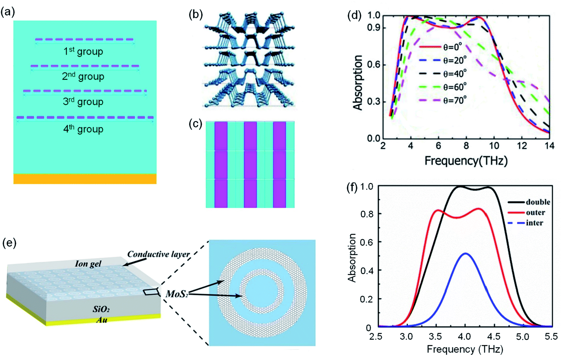
Because of the resemble properties observed in 2D materials, other 2D materials such as phosphorene (2D black phosphorus)122–130 and molybdenum disulfide (MoS2)131 were also studied for THz protection in recent research. Based on the SPPs and localized plasmon resonance in phosphorene, it was convenient to produce THz-absorbing MMs comprised of period structural phosphorene arrays. Wang et al.127 designed ultra-wideband MMs by assembling dozens of phosphorene/dielectric pairs with different widths, in which the meta-structures were divided into 4 groups and distributed in 4 layers (Fig. 12a–c). The widths of the phosphorene stripes were identical in each group and different in distinct groups. Because of the asymmetrical structure and strong anisotropy, the simulated THz absorption results of the phosphorene MMs absorber showed that the absorption above 90% could cover 3.4–9.6 THz for normal incidence, while the absorber could retain high and ultra-wideband absorption within the incident angle of around 40° (Fig. 12d). In addition, as a typical 2D semiconductor with unique electrical, optical and magnetic properties, transition-metal dichalcogenides (MoS2) were also studied to design THz-absorbing MMs. Wang et al.131 proposed angle-insensitive THz absorbing MMs composed of a monolayer MoS2 concentric double ring (MCDR) metastructure and a metal film separated by a dielectric layer (Fig. 12e). For the plasma hybridization caused by the lateral coupling between the two separate MoS2 rings, the THz absorption bandwidth and effectiveness could both be improved. Moreover, due to its special concentric structures, the absorber was insensitive to the incident angles and polarizations of the THz sources. Compared to the MoS2 single ring (MSR) MMs with only separate outer or inter rings, the calculated results confirmed that the MCDRs absorber demonstrates obviously superior THz absorption in a wider THz waveband (Fig. 12f).
 |
| | Fig. 12 (a) Unit cell, (b) structural details in each group, (c) top view across one phosphorene section and (d) THz absorption curves of phosphorene MMs (reproduced with permission from ref. 127 Copyright 2019 Springer Nature). (e) Schematic structure of the proposed THz-absorbing MMs comprising MCDRs and gold metal separated by a thin layer of silicon dioxide. (f) THz absorption curves of the designed MCDR absorber and MSR absorbers (reproduced with permission from ref. 131 Copyright 2019 Elsevier). | |
5. Summary and perspectives
With unique THz response characteristics, MM absorbers based on 2D materials in the forms of single layer, multiple layers, hybrid and tunable metasurfaces showed excellent THz absorbing performance. Recent advances in this field provided a sufficient theoretical and practical basis for THz protection, and the superior properties of 2D material MMs endow them with wide application prospects. However, due to the preparation limitations of the patterned 2D material metasurfaces, current research is mostly focused on theoretical designs and simulations, which has slowed the practical application of 2D material MMs. In addition, 3D intrinsic THz absorbing materials based on porous or ordered 2D materials show exceptional THz protection performance; they effectively integrate the advantages of the intrinsic properties and structural characteristics of 2D materials. These special structures could optimize the surface impedance matching and form THz multiple scattering and electric transmission loss, which could realize high-efficiency absorption loss and active controllable protection performance in a wide THz waveband. Without considering the material thickness, 3D porous THz protection materials are more suitable for practical application in high-performance THz protection devices. Some typical THz protection materials and their performance are summarized and listed in Table 1.
Table 1 Typical THz protection materials
| Sample |
Absorption |
Effective bandwidth |
Shielding effectiveness |
Active control excitations |
Ref. |
| Graphene/SiO2/p-Si/Au MMs |
∼0.8@620 GHz |
— |
— |
Electric field |
110
|
| Graphene/polymer/Au MMs |
0.95@0.5 THz, 0.97@1.5 THz |
— |
— |
— |
56
|
| Porous graphene/cross-shape Au/liquid crystal/Au MMs |
0.96@1THz (TM), 0.97@0.87THz (TE) |
— |
— |
Electric field |
95
|
| MXene/Au nano-slot MMs |
— |
— |
20 dB@1.0 THz |
— |
13
|
| Patterned graphene/PI/Au MMs |
— |
1.54–2.23 THz |
|
|
108
|
| Ion gel/graphene/stripe Al/PI/Al MMs |
∼20 dB@0.43 & 0.75 THz |
— |
— |
Electric field |
103
|
| rGO paper |
17.6 dB@0.7 THz |
— |
72.1 dB@ 0.6 THz |
— |
132
|
| 3D rGO foam |
28 dB@1.6 THz |
0.2–1.6 THz |
28 dB@1.6 THz |
Electric and optical field |
10 and 36 |
| WCNT/rGO foam |
30 dB |
1.5 THz (0.1–1.6 THz) |
61 dB |
|
33
|
| Fe3O4/rGO foam |
38 dB (average) |
3.4 GHz–2.5 THz |
|
|
35
|
| MXene/rGO foam |
30.6 dB (average) |
0.2–2.0 THz |
|
|
37
|
| MXene/GO/Zn2+ foam |
|
0.86–2.0 THz |
51 dB |
|
16
|
The THz protection materials in future 6G applications should meet application requirements such as reduced dimensions, light weight, wide effective absorption bandwidth and high absorbing ability. Meanwhile, THz protection materials should also realize tunable THz protection performance. For THz protection MMs, the advances in nanomaterials science and nano-manufacturing technology should be adopted to realize enhanced THz protection and tunable characteristics of 2D materials, and the device integration fabrication ability should be fully considered to improve their performance in practical applications. For THz intrinsic protection materials, the influence of intrinsic properties (scale, defects, functional groups and flake sizes, etc.), inner nanostructures (hole structure or layer spacing, etc.) and doping behaviors with other loss materials (dielectric or magnetic particles, etc.) on the THz responses should be systematically studied.
Conflicts of interest
There are no conflicts to declare.
References
- S. Dang,
et al., What should 6G be?, Nat. Electron., 2020, 3(1), 20–29 CrossRef.
- I. F. Akyildiz, J. M. Jornet and C. Han, Terahertz band: next frontier for wireless communications, Phys. Commun., 2014, 12, 16–32 CrossRef.
- J. Federici and L. Moeller, Review of terahertz and subterahertz wireless communications, J. Appl. Phys., 2010, 107(11), 22 CrossRef.
- D. M. Mittleman, Perspective: terahertz science and technology, J. Appl. Phys., 2017, 122(23), 230901 CrossRef.
- T. J. Yen,
et al., Terahertz Magnetic Response from Artificial Materials, Science, 2004, 303(5663), 1494 CrossRef CAS.
- H. Tao,
et al., A metamaterial absorber for the terahertz regime: design, fabrication and characterization, Opt. Express, 2008, 16(10), 7181–7188 CrossRef.
- Y. Zhang,
et al., Broadband and Tunable High-Performance Microwave Absorption of an Ultralight and Highly Compressible Graphene Foam, Adv. Mater., 2015, 27(12), 2049–2053 CrossRef CAS.
- B. Wen,
et al., Reduced Graphene Oxides: Light-Weight and High-Efficiency Electromagnetic Interference Shielding at Elevated Temperatures, Adv. Mater., 2014, 26(21), 3484–3489 CrossRef CAS.
- F. Shahzad,
et al., Electromagnetic interference shielding with 2D transition metal carbides (MXenes), Science, 2016, 353(6304), 1137–1140 CrossRef CAS.
- Z. Huang,
et al., Ultra-Broadband Wide-Angle Terahertz Absorption Properties of 3D Graphene Foam, Adv. Funct. Mater., 2018, 28(2), 1704363 CrossRef.
- M. Zdrojek,
et al., Graphene-based plastic absorber for total sub-terahertz radiation shielding, Nanoscale, 2018, 10(28), 13426–13431 RSC.
- H. H. Chen,
et al., Graphene-Based Materials toward Microwave and Terahertz Absorbing Stealth Technologies, Adv. Opt. Mater., 2019, 7(8), 16 Search PubMed.
- G. Choi,
et al., Enhanced Terahertz Shielding of MXenes with Nano-Metamaterials, Adv. Opt. Mater., 2018, 6(5), 1701076 CrossRef.
- M. Amin, M. Farhat and H. Bağcı, An ultra-broadband multilayered graphene absorber, Opt. Express, 2013, 21(24), 29938–29948 CrossRef.
- M. Rahmanzadeh, H. Rajabalipanah and A. Abdolali, Multilayer graphene-based metasurfaces: robust design method for extremely broadband, wide-angle, and polarization-insensitive terahertz absorbers, Appl. Opt., 2018, 57(4), 959–968 CrossRef CAS.
- Z. Lin,
et al., Highly Stable 3D Ti3C2Tx MXene-Based Foam Architectures toward High-Performance Terahertz Radiation Shielding, ACS Nano, 2020, 14(2), 2109–2117 CrossRef CAS.
- V. Bianchi,
et al., Terahertz saturable absorbers from liquid phase exfoliation of graphite, Nat. Commun., 2017, 8, 9 CrossRef.
- L. F. Ye,
et al., Composite graphene-metal microstructures for enhanced multiband absorption covering the entire terahertz range, Carbon, 2019, 148, 317–325 CrossRef CAS.
- N. I. Landy,
et al., Perfect Metamaterial Absorber, Phys. Rev. Lett., 2008, 100(20), 207402 CrossRef CAS.
- P. Yu,
et al., Broadband Metamaterial Absorbers, Adv. Opt. Mater., 2019, 7(3), 1800995 CrossRef.
- G. Duan,
et al., A survey of theoretical models for terahertz electromagnetic metamaterial absorbers, Sens. Actuators, A, 2019, 287, 21–28 CrossRef CAS.
- S. Liu and T. J. Cui, Concepts, Working Principles, and Applications of Coding and Programmable Metamaterials, Adv. Opt. Mater., 2017, 5(22), 1700624 CrossRef.
- M. Kenney,
et al., Octave-Spanning Broadband Absorption of Terahertz Light Using Metasurface Fractal-Cross Absorbers, ACS Photonics, 2017, 4(10), 2604–2612 CrossRef CAS.
- H. Tao,
et al., Highly flexible wide angle of incidence terahertz metamaterial absorber: design, fabrication, and characterization, Phys. Rev. B: Condens. Matter Mater. Phys., 2008, 78(24), 4 CrossRef.
- N. I. Landy,
et al., Design, theory, and measurement of a polarization-insensitive absorber for terahertz imaging, Phys. Rev. B: Condens. Matter Mater. Phys., 2009, 79(12), 6 CrossRef.
- M. Wu,
et al., A three-dimensional all-metal terahertz metamaterial perfect absorber, Appl. Phys. Lett., 2017, 111(5), 051101 CrossRef.
- Q. H. Song,
et al., Liquid-metal-based metasurface for terahertz absorption material: frequency-agile and wide-angle, APL Mater., 2017, 5(6), 066103 CrossRef.
- Z. H. Xu,
et al., Design of a Tunable Ultra-Broadband Terahertz Absorber Based on Multiple Layers of Graphene Ribbons, Nanoscale Res. Lett., 2018, 13, 8 CrossRef.
- E. Galiffi, J. B. Pendry and P. A. Huidobro, Broadband Tunable THz Absorption with Singular Graphene Metasurfaces, ACS Nano, 2018, 12(2), 1006–1013 CrossRef CAS.
- Z. Fei,
et al., Gate-tuning of graphene plasmons revealed by infrared nano-imaging, Nature, 2012, 487(7405), 82–85 CrossRef CAS.
- R. J. Xu, X. Y. Liu and Y. S. Lin, Tunable ultra-narrowband terahertz perfect absorber by using metal-insulator-metal microstructures, Results Phys., 2019, 13, 102176 CrossRef.
- Z. Song,
et al., Wide-angle absorber with tunable intensity and bandwidth realized by a terahertz phase change material, Opt. Commun., 2020, 464, 125494 CrossRef CAS.
- Z. Y. Huang,
et al., Graphene-Based Composites Combining Both Excellent Terahertz Shielding and Stealth Performance, Adv. Opt. Mater., 2018, 6(23), 9 Search PubMed.
- Z. Y. Huang,
et al., Research Progress on Terahertz Stealth and Shielding Materials, Chem. J. Chin. Univ., 2019, 40(6), 1103–1115 CAS.
- H. Chen,
et al., Consecutively Strong Absorption from Gigahertz to Terahertz Bands of a Monolithic Three-Dimensional Fe3O4/Graphene Material, ACS Appl. Mater. Interfaces, 2019, 11(1), 1274–1282 CrossRef CAS.
- S.-T. Xu,
et al., Active Terahertz Shielding and Absorption Based on Graphene Foam Modulated by Electric and Optical Field Excitation, Adv. Opt. Mater., 2019, 7(18), 1900555 CrossRef.
- W. L. Ma,
et al., Compressible Highly Stable 3D Porous MXene/GO Foam with a Tunable High-Performance Stealth Property in the Terahertz Band, ACS Appl. Mater. Interfaces, 2019, 11(28), 25369–25377 CrossRef CAS.
- A. Andryieuski and A. V. Lavrinenko, Graphene metamaterials based tunable terahertz absorber: effective surface conductivity approach, Opt. Express, 2013, 21(7), 9144–9155 CrossRef CAS.
- R.-M. Gao,
et al., Intensity-modulating graphene metamaterial for multiband terahertz absorption, Appl. Opt., 2016, 55(8), 1929–1933 CrossRef CAS.
- B. Wu,
et al., Experimental demonstration of a transparent graphene millimetre wave absorber with 28% fractional bandwidth at 140 GHz, Sci. Rep., 2014, 4(1), 4130 CrossRef.
- R. Jadeja,
et al., Numerical investigation of graphene-based efficient and broadband metasurface for terahertz solar absorber, J. Mater. Sci., 2020, 55(8), 3462–3469 CrossRef CAS.
- K. Batrakov,
et al., Enhanced microwave-to-terahertz absorption in graphene, Appl. Phys. Lett., 2016, 108(12), 4 CrossRef.
- Y. X. Zhou,
et al., Terahertz wave reflection impedance matching properties of graphene layers at oblique incidence, Carbon, 2016, 96, 1129–1137 CrossRef CAS.
- D. D. Sun,
et al., Enhanced spatial terahertz modulation based on graphene metamaterial, Chin. Opt. Lett., 2017, 15(5), 4 Search PubMed.
- C. L. Cen,
et al., Plasmonic absorption characteristics based on dumbbell-shaped graphene metamaterial arrays, Phys. E, 2018, 103, 93–98 CrossRef CAS.
- C. L. Cen,
et al., Tunable plasmonic resonance absorption characteries-tics in periodic H-shaped graphene arrays, Superlattices Microstruct., 2018, 120, 427–435 CrossRef CAS.
- C. Liu, L. M. Qi and X. Zhang, Broadband graphene-based metamaterial absorbers, AIP Adv., 2018, 8(1), 7 Search PubMed.
- C. L. Cen,
et al., Tunable absorption enhancement in periodic elliptical hollow graphene arrays, Opt. Mater. Express, 2019, 9(2), 706–716 CrossRef CAS.
- Y. J. Li,
et al., Tunable quintuple-band polarization-insensitive wide-angle metamaterial absorber with single-layered graphene in terahertz range, Mater. Res. Express, 2019, 6(8), 8 Search PubMed.
- Z. M. Liu, L. Guo and Q. M. Zhang, A Simple and Efficient Method for Designing Broadband Terahertz Absorber Based on Singular Graphene Metasurface, Nanomaterials, 2019, 9(10), 9 Search PubMed.
- Y. Qi,
et al., Tunable plasmonic absorber in THz-band range based on graphene “arrow” shaped metamaterial, Results Phys., 2019, 15, 102777 CrossRef.
- S. Wu,
et al., Graphene-based single-layer elliptical pattern metamaterial absorber for adjustable broadband absorption in terahertz range, Phys. Scr., 2019, 94(10), 8 Search PubMed.
- D. X. Yan and J. S. Li, Tunable all-graphene-dielectric single-band terahertz wave absorber, J. Phys. D: Appl. Phys., 2019, 52(27), 7 CrossRef.
- F. Chen, Y. Z. Cheng and H. Luo, A Broadband Tunable Terahertz Metamaterial Absorber Based on Single-Layer Complementary Gammadion-Shaped Graphene, Materials, 2020, 13(4), 11 Search PubMed.
- B. Sensale-Rodriguez,
et al., Efficient terahertz electro-absorption modulation employing graphene plasmonic structures, Appl. Phys. Lett., 2012, 101(26), 3 CrossRef.
- J. Min Woo,
et al., Graphene based salisbury screen for terahertz absorber, Appl. Phys. Lett., 2014, 104(8), 081106 CrossRef.
- Z. Yi,
et al., Tunable Graphene-based Plasmonic Perfect Metamaterial Absorber in the THz Region, Micromachines, 2019, 10(3), 11 CrossRef.
- Y. Wang,
et al., Staked Graphene for Tunable Terahertz Absorber with Customized Bandwidth, Plasmonics, 2016, 11(5), 1201–1206 CrossRef CAS.
- B. Xiao, M. Gu and S. Xiao, Broadband, wide-angle and tunable terahertz absorber based on cross-shaped graphene arrays, Appl. Opt., 2017, 56(19), 5458–5462 CrossRef CAS.
- J. G. Zhang, J. P. Tian and L. Li, A Dual-Band Tunable Metamaterial Near-Unity Absorber Composed of Periodic Cross and Disk Graphene Arrays, IEEE Photonics J., 2018, 10(2), 12 Search PubMed.
- Z. Yi,
et al., Tunable dual-band perfect absorber consisting of periodic cross-cross monolayer graphene arrays, Results Phys., 2019, 13, 102217 CrossRef.
- K. Arik, S. AbdollahRamezani and A. Khavasi, Polarization Insensitive and Broadband Terahertz Absorber Using Graphene Disks, Plasmonics, 2017, 12(2), 393–398 CrossRef CAS.
- R. Alaee,
et al., A perfect absorber made of a graphene micro-ribbon metamaterial, Opt. Express, 2012, 20(27), 28017–28024 CrossRef CAS.
- Z. H. Zhu,
et al., Broadband single-layered graphene absorber using periodic arrays of graphene ribbons with gradient width, Appl. Phys. Express, 2015, 8(1), 3 Search PubMed.
- S. Y. Xiao,
et al., Tunable light trapping and absorption enhancement with graphene ring arrays, Phys. Chem. Chem. Phys., 2016, 18(38), 26661–26669 RSC.
- N. L. Mou,
et al., Hybridization-induced broadband terahertz wave absorption with graphene metasurfaces, Opt. Express, 2018, 26(9), 11728–11736 CrossRef CAS.
- P. Kumar, A. Lakhtakia and P. K. Jain, Graphene pixel-based polarization-insensitive metasurface for almost perfect and wideband terahertz absorption, J. Opt. Soc. Am. B, 2019, 36(8), F84–F88 CrossRef CAS.
- R. M. Gao,
et al., Graphene metamaterial for multiband and broadband terahertz absorber, Opt. Commun., 2015, 356, 400–404 CrossRef CAS.
- P. C. Wu, N. Papasimakis and D. P. Tsai, Self-Affine Graphene Metasurfaces for Tunable Broadband Absorption, Phys. Rev. Appl., 2016, 6(4), 8 Search PubMed.
- S. L. He and T. Chen, Broadband THz Absorbers With Graphene-Based Anisotropic Metamaterial Films, IEEE Trans. Terahertz Sci. Technol., 2013, 3(6), 757–763 CAS.
- M. Faraji, M. K. Morawej-Farshi and L. Yousefi, Tunable THz perfect absorber using graphene-based metamaterials, Opt. Commun., 2015, 355, 352–355 CrossRef CAS.
- Y. Q. Wang,
et al., Staked Graphene for Tunable Terahertz Absorber with Customized Bandwidth, Plasmonics, 2016, 11(5), 1201–1206 CrossRef CAS.
- M. Chen,
et al., Frequency-tunable terahertz absorbers based on graphene metasurface, Opt. Commun., 2017, 382, 144–150 CrossRef CAS.
- S. Biabanifard,
et al., Tunable ultra-wideband terahertz absorber based on graphene disks and ribbons, Opt. Commun., 2018, 427, 418–425 CrossRef CAS.
- P. Fu,
et al., A broadband metamaterial absorber based on multi-layer graphene in the terahertz region, Opt. Commun., 2018, 417, 62–66 CrossRef CAS.
- R. Xing and S. S. Jian, A dual-band THz absorber based on graphene sheet and ribbons, Opt. Laser Technol., 2018, 100, 129–132 CrossRef CAS.
- R. Mishra, A. Sahu and R. Panwar, Cascaded Graphene Frequency Selective Surface Integrated Tunable Broadband Terahertz Metamaterial Absorber, IEEE Photonics J., 2019, 11(2), 2200310 CAS.
- M. Soltani,
et al., A configurable two-layer four-bias graphene-based THz absorber, J. Comput. Electron., 2020, 19(2), 719–735 CrossRef CAS.
- G. S. Deng,
et al., Graphene-based tunable polarization sensitive terahertz metamaterial absorber, Opt. Commun., 2016, 380, 101–107 CrossRef CAS.
- E. S. Torabi, A. Fallahi and A. Yahaghi, Evolutionary Optimization of Graphene-Metal Metasurfaces for Tunable Broadband Terahertz Absorption, IEEE Trans. Antennas Propag., 2017, 65(3), 1464–1467 Search PubMed.
- Z. P. Wang and Y. M. Hou, Ultra-multiband absorption enhancement of graphene in a metal-dielectric-graphene sandwich structure covering terahertz to mid-infrared regime, Opt. Express, 2017, 25(16), 19185–19194 CrossRef CAS.
- Y. T. Zhao,
et al., Switchable broadband terahertz absorber/reflector enabled by hybrid graphene-gold metasurface, Opt. Express, 2017, 25(7), 7161–7169 CrossRef CAS.
- C. Shi,
et al., Investigation of graphene-supported tunable asymmetric terahertz metamaterials, J. Opt. Soc. Am. B, 2018, 35(3), 575–581 CrossRef CAS.
- T. V. Huynh,
et al., Controlling the absorption strength in bidirectional terahertz metamaterial absorbers with patterned graphene, Comput. Mater. Sci., 2019, 166, 276–281 CrossRef.
- L. Peng,
et al., Metal and graphene hybrid metasurface designed ultra-wideband terahertz absorbers with polarization and incident angle insensitivity, Nanoscale Adv., 2019, 1(4), 1452–1459 RSC.
- L. M. Qi and C. Liu, Broadband multilayer graphene metamaterial absorbers, Opt. Mater. Express, 2019, 9(3), 1298–1309 CrossRef CAS.
- M. R. Soheilifar and F. B. Zarrabi, Reconfigurable metamaterial absorber as an optical switch based on organic-graphene control, Opt. Quantum Electron., 2019, 51(5), 12 CrossRef.
- X. M. Zhang,
et al., A Dual-Band Terahertz Absorber with Two Passbands Based on Periodic Patterned Graphene, Materials, 2019, 12(18), 3016 CrossRef CAS.
- X. H. Deng,
et al., Tunable THz absorption in graphene-based heterostructures, Opt. Express, 2014, 22(24), 30177–30183 CrossRef.
- X. He,
et al., Investigation of graphene assisted tunable terahertz metamaterials absorber, Opt. Mater. Express, 2016, 6(2), 331–342 CrossRef CAS.
- Q. H. Zhou,
et al., Controlling enhanced absorption in graphene metamaterial, Opt. Commun., 2018, 413, 310–316 CrossRef CAS.
- L. M. Qi, C. Liu and S. M. A. Shah, A broad dual-band switchable graphene-based terahertz metamaterial absorber, Carbon, 2019, 153, 179–188 CrossRef CAS.
- A. Soleymani, R. E. Meymand and N. Granpayeh, Broadband near-perfect terahertz absorber in single-layered and non-structured graphene loaded with dielectrics, Appl. Opt., 2020, 59(9), 2839–2848 CrossRef CAS.
- H. Zhang,
et al., A water hybrid graphene metamaterial absorber with broadband absorption, Opt. Commun., 2020, 463, 125394 CrossRef CAS.
- L. Wang,
et al., Graphene-assisted high-efficiency liquid crystal tunable terahertz metamaterial absorber, Opt. Express, 2017, 25(20), 23873–23879 CrossRef CAS.
- Y. C. Fan,
et al., Broadband Terahertz Absorption in Graphene-Embedded Photonic Crystals, Plasmonics, 2018, 13(4), 1153–1158 CrossRef CAS.
- B.-z. Xu,
et al., A novel structure for tunable terahertz absorber based on graphene, Opt. Express, 2013, 21(20), 23803–23811 CrossRef CAS.
- Y. Zhang,
et al., Graphene based tunable metamaterial absorber and polarization modulation in terahertz frequency, Opt. Express, 2014, 22(19), 22743–22752 CrossRef.
- X. He,
et al., Active graphene metamaterial absorber for terahertz absorption bandwidth, intensity and frequency control, Opt. Mater. Express, 2018, 8(4), 1031–1042 CrossRef CAS.
- X. Huang,
et al., Polarization-independent and angle-insensitive broadband absorber with a target-patterned graphene layer in the terahertz regime, Opt. Express, 2018, 26(20), 25558–25566 CrossRef CAS.
- Y. Jiang,
et al., Design and performance of a terahertz absorber based on patterned graphene, Opt. Lett., 2018, 43(17), 4296–4299 CrossRef CAS.
- L. Qi, C. Liu and S. M. A. Shah, A broad dual-band switchable graphene-based terahertz metamaterial absorber, Carbon, 2019, 153, 179–188 CrossRef CAS.
- X. Chen,
et al., Electrically Tunable Perfect Terahertz Absorber Based on a Graphene Salisbury Screen Hybrid Metasurface, Adv. Opt. Mater., 2020, 8(3), 1900660 CrossRef CAS.
- X. Jin,
et al., Coherent perfect absorber with independently tunable frequency based on multilayer graphene, Opt. Commun., 2019, 446, 44–50 CrossRef CAS.
- Z. Xu,
et al., Design of a Tunable Ultra-Broadband Terahertz Absorber Based on Multiple Layers of Graphene Ribbons, Nanoscale Res. Lett., 2018, 13(1), 143 CrossRef.
- M. Y. Gu, B. G. Xiao and S. S. Xiao, Tunable THz perfect absorber with two absorption peaks based on graphene microribbons, Micro Nano Lett., 2018, 13(5), 631–635 CrossRef CAS.
- X. J. He,
et al., Active graphene metamaterial absorber for terahertz absorption bandwidth, intensity and frequency control, Opt. Mater. Express, 2018, 8(4), 1031–1042 CrossRef CAS.
- Y. Jiang,
et al., Design and performance of a terahertz absorber based on patterned graphene, Opt. Lett., 2018, 43(17), 4296–4299 CrossRef CAS.
- S. H. Lee,
et al., Switching terahertz waves with gate-controlled active graphene metamaterials, Nat. Mater., 2012, 11(11), 936–941 CrossRef CAS.
- B. Sensale-Rodriguez,
et al., Extraordinary Control of Terahertz Beam Reflectance in Graphene Electro-absorption Modulators, Nano Lett., 2012, 12(9), 4518–4522 CrossRef CAS.
- R. Cheng,
et al., Tunable graphene-based terahertz absorber via an external magnetic field, Opt. Mater. Express, 2020, 10(2), 501–512 CrossRef CAS.
- M. B. Heydari and M. H. V. Samiei, An Analytical Study of Magneto-Plasmons in Anisotropic Multi-layer Structures Containing Magnetically Biased Graphene Sheets, Plasmonics, 2020, 16 Search PubMed.
- A. C. Tasolamprou,
et al., Experimental Demonstration of Ultrafast THz Modulation in a Graphene-Based Thin Film Absorber through Negative Photoinduced Conductivity, ACS Photonics, 2019, 6(3), 720–727 CrossRef CAS.
- S. Borzooei, E. Rezagholizadeh and M. Biabanifard, Graphene disks for frequency control of terahertz waves in broadband applications, J. Comput. Electron., 2020, 19(2), 759–772 CrossRef CAS.
- J. S. Li,
et al., Flexible electromagnetic wave absorbing composite based on 3D rGO-CNT-Fe3O4 ternary films, Carbon, 2018, 129, 76–84 CrossRef CAS.
- Z. Huang,
et al., Graphene-Based Composites Combining Both Excellent Terahertz Shielding and Stealth Performance, Adv. Opt. Mater., 2018, 6(23), 1801165 CrossRef.
- G. Li,
et al., Dynamical Control over Terahertz Electromagnetic Interference Shielding with 2D Ti3C2Ty MXene by Ultrafast Optical Pulses, Nano Lett., 2020, 20(1), 636–643 CrossRef CAS.
- K. Hantanasirisakul and Y. Gogotsi, Electronic and Optical Properties of 2D Transition Metal Carbides and Nitrides (MXenes), Adv. Mater., 2018, 30(52), 1804779 CrossRef.
- H. Wang,
et al., Clay-Inspired MXene-Based Electrochemical Devices and Photo-Electrocatalyst: State-of-the-Art Progresses and Challenges, Adv. Mater., 2018, 30(12), 1704561 CrossRef.
- T. Yun,
et al., Electromagnetic Shielding of Monolayer MXene Assemblies, Adv. Mater., 2020, 32(9), 9 Search PubMed.
- Y. I. Jhon, M. Seo and Y. M. Jhon, First-principles study of a MXene terahertz detector, Nanoscale, 2018, 10(1), 69–75 RSC.
- Y. M. Qing, H. F. Ma and T. J. Cui, Tailoring anisotropic perfect absorption in monolayer black phosphorus by critical coupling at terahertz frequencies, Opt. Express, 2018, 26(25), 32442–32450 CrossRef CAS.
- X. Wang,
et al., Tunable terahertz/infrared coherent perfect absorption in a monolayer black phosphorus, Opt. Express, 2018, 26(5), 5488–5496 CrossRef CAS.
- D. X. Dong,
et al., Tunable THz reflection-type polarizer based on monolayer phosphorene, Appl. Opt., 2019, 58(35), 9643–9650 CrossRef CAS.
- Y. N. Jiang,
et al., Broadband linear-to-circular polarization converter based on phosphorene metamaterial, Opt. Mater. Express, 2019, 9(5), 2088–2097 CrossRef CAS.
-
G. Tianjing and C. Argyropoulos, Polarization-Independent and Broadband THz Coherent Perfect Absorber based on Black Phosphorus Bifacial Metasurfaces, in 2019 IEEE International Symposium on Antennas and Propagation and USNC-URSI Radio Science Meeting, 2019, IEEE, pp. 567–568 Search PubMed.
- J. Wang and Y. N. Jiang, A phosphorene-based metasurface absorber operating in ultra-wideband terahertz regime, Eur. Phys. J. D, 2019, 73(12), 255 CrossRef CAS.
- Y. J. Cai,
et al., Investigation of multi-resonant and anisotropic plasmonic resonances in the stacked graphene-black phosphorus bilayers, J. Phys. D: Appl. Phys., 2020, 53(2), 025107 CrossRef CAS.
- T. T. Liu,
et al., Tunable anisotropic absorption in monolayer black phosphorus using critical coupling, Appl. Phys. Express, 2020, 13(1), 5 Search PubMed.
- W. Tongling,
et al., Tunable broadband terahertz metamaterial absorber using multi-layer black phosphorus and vanadium dioxide, J. Phys. D: Appl. Phys., 2020, 53(14), 145105 CrossRef.
- X. Y. Wang,
et al., Angle insensitive broadband terahertz wave absorption based on molybdenum disulfide metamaterials, Superlattices Microstruct., 2019, 135, 5 Search PubMed.
- S. Dong,
et al., Flexible reduced graphene oxide paper with excellent electromagnetic interference shielding for terahertz wave, J. Mater. Sci.: Mater. Electron., 2018, 29(20), 17245–17253 CrossRef CAS.
|
| This journal is © The Royal Society of Chemistry 2021 |
Click here to see how this site uses Cookies. View our privacy policy here. 
 Open Access Article
 This Open Access Article is licensed under a Creative Commons Attribution-Non Commercial 3.0 Unported Licence
 *a
*a