
 Open Access Article
 This Open Access Article is licensed under a Creative Commons Attribution-Non Commercial 3.0 Unported Licence
A wafer-scale synthesis of monolayer MoS2 and their field-effect transistors toward practical applications
Yuchun
Liu
and
Fuxing
Gu
 *
*
Laboratory of Integrated Opto-Mechanics and Electronics, School of Optical-Electrical and Computer Engineering, University of Shanghai for Science and Technology, Shanghai 200093, China. E-mail: gufuxing@usst.edu.cn
First published on 23rd February 2021
Abstract
Molybdenum disulfide (MoS2) has attracted considerable research interest as a promising candidate for downscaling integrated electronics due to the special two-dimensional structure and unique physicochemical properties. However, it is still challenging to achieve large-area MoS2 monolayers with desired material quality and electrical properties to fulfill the requirement for practical applications. Recently, a variety of investigations have focused on wafer-scale monolayer MoS2 synthesis with high-quality. The 2D MoS2 field-effect transistor (MoS2-FET) array with different configurations utilizes the high-quality MoS2 film as channels and exhibits favorable performance. In this review, we illustrated the latest research advances in wafer-scale monolayer MoS2 synthesis by different methods, including Au-assisted exfoliation, CVD, thin film sulfurization, MOCVD, ALD, VLS method, and the thermolysis of thiosalts. Then, an overview of MoS2-FET developments was provided based on large-area MoS2 film with different device configurations and performances. The different applications of MoS2-FET in logic circuits, basic memory devices, and integrated photodetectors were also summarized. Lastly, we considered the perspective and challenges based on wafer-scale monolayer MoS2 synthesis and MoS2-FET for developing practical applications in next-generation integrated electronics and flexible optoelectronics.
 Yuchun Liu | Yuchun Liu received her PhD from Huazhong University of Science and Technology in 2017. She is now a postdoctoral researcher at the University of Shanghai for Science and Technology with Prof. Songlin Zhuang and Prof. Fuxing Gu. Her research interests focus on the synthesis and understanding the mechanism of two-dimensional materials and their applications in optics and optoelectronics, including transition metal dichalcogenides and inorganic perovskites. |
 Fuxing Gu | Fuxing Gu received his BS degree in 2006 and PhD degree in 2012 from Zhejiang University. He is currently an associate professor at the Laboratory of Integrated Opto-Mechanics and Electronics (https://iome.usst.edu.cn), University of Shanghai for Science and Technology, China. His research interests include micro/nanofiber optics and opto-mechanics, microcavity, and 2D-material optics. He has published over 40 papers in journals such as Science, Nat. Commun., Sci. Adv., Light: Sci. & Appl., J. Am. Chem. Soc., and Nano Lett. |
1. Introduction
In recent years, 2D transition metal dichalcogenides (TMD), especially molybdenum disulfide (MoS2), have attracted widespread attention for a variety of next-generation electronic and optoelectronic device applications.1–3 Compared with conventional silicon-based semiconductors, monolayer MoS2 is envisioned as an alternate building block for the next-generation electronic device and integrated circuit with short channel, thin thickness, small volume, light weight, fast speed, and high sensitivity.4–12 However, it is still very challenging to achieve large-area, high-quality MoS2 for practical applications. Since the traditional mechanical exfoliation method is difficult to meet the needs of wafer-scale MoS2 synthesis in terms of the yield, size, thickness, and uniformity, most MoS2 investigations synthesis have focused on developing the vapor phase growth of monolayer MoS2.13–15 Generally, synthetic methods for large-area monolayers and few-layer MoS2 films include traditional chemical vapor deposition (CVD), thin film sulfurization, metal–organic chemical vapor deposition (MOCVD), atomic layer deposition (ALD), and vapor–liquid–solid (VLS) method.16–28 Due to the development of synthetic methods, the large-area, high-quality continuous monolayer MoS2 films have been successfully reported, with a wafer-scale even up to 8 inch,18 suggesting great potential in integrated devices compatible with silicon-based micro-fabrication processes.In the past decade, 2D MoS2 with atomic thickness is considered one of the most promising candidates for the downscaling trend in integrated electronics, which leads to continuing demands for minimizing the channel thickness. The wafer-scale 2D MoS2 films can be reliably transferred and heterogeneously integrated onto a variety of substrates with the aid of polymethyl methacrylate (PMMA) or olydimethylsiloxane (PDMS), demonstrating many important applications in environment-friendly transient devices.11–13,31 Since the fabrication process of wafer-scale MoS2-based devices can be more compatible with the traditional complementary metal oxide semiconductor (CMOS) fabrication process, many investigations have focused on developing wafer-scale monolayer MoS2 and high-performance MoS2 field-effect transistors (MoS2-FET) to significantly promote their future device applications, especially electronic and optoelectronic applications.11–13 The fabricated MoS2-FET have achieved attractive performance with high on/off ratios up to 1010 and a high mobility of about 167 ± 20 cm2 V−1 s−1.13,14 Even though the reported field effect mobility of MoS2-FET is still behind that of Si-based transistors, explorations are promising to advance one step further from a single MoS2-FET to complex devices, such as basic logic gate circuits, basic memory devices, and integrated phototransistors. With the development of MoS2 synthesis and FET techniques, 2D MoS2 would play a great role in next-generation integrated circuits and flexible electronics.
In this review, we focus on wafer-scale synthesis of monolayer MoS2 film and the high-performance MoS2-FET toward practical applications. We first introduce the recent progresses in MoS2 synthesis by different methods, including Au-assisted exfoliation, CVD, thin film sulfurization, MOCVD, ALD, VLS method, and the thermolysis of thiosalts. Then, an overview of the MoS2-FET developments will be provided based on different device configurations. The basic characterization and device performance of different MoS2-FET will also be summarized. Furthermore, we will present recent advances in applications of logic circuits, memory devices, and photodetectors based on 2D wafer-scale monolayer MoS2 and MoS2-FET. Lastly, we will discuss the perspective and challenges based on wafer-scale MoS2 synthesis and MoS2-FET for developing practical applications in integrated electronics and flexible optoelectronics. The recent advances in monolayer MoS2 synthesis and MoS2-FETs emphasize the opportunity and potential of the wafer-scale MoS2 in terms of achieving the practical application in modern large-scale integrated devices based on the existing silicon-based micro-fabrication processes.
2. Wafer-scale MoS2 synthesis
2D MoS2 film can be synthesized by the top-down strategy and the bottom-up strategy. In the top-down strategy, the commercialized MoS2 bulk crystal is physically peeled into the monolayer or few-layer MoS2 flakes by mechanical exfoliation methods. In the bottom-up strategy, the MoS2 film is prepared through chemical reaction on a specific substrate by CVD, MOCVD, ALD, etc. In order to realize wafer-scale monolayer MoS2 synthesis, continuous efforts have been made to develop the synthetic method and synthetic system based on the top-down strategy and the bottom-up strategy.2.1 Au-assisted exfoliation method
Due to the unique layered geometry and van der Waals (vdW) interactions in 2D materials, mechanical exfoliation provides a low-cost way to produce the monolayer and few-layer highly crystalline layered 2D materials. In a typical mechanical exfoliation process, appropriate thin MoS2 crystals were first peeled off from the bulk crystal using adhesive scotch tape and then transferred onto a target substrate. After the scotch tape is removed, monolayer or few-layer MoS2 can be obtained on the substrate. Generally, the sizes and thicknesses of 2D MoS2 from scotch-tape exfoliation are limited, which is not suitable for mass-production and scaled-up applications. Gold is known to have a strong affinity for sulfur and can be exploited to exfoliate monolayer from the bulk crystal as a result of strong vdW interactions between Au and the topmost MoS2 layer.26–28Recently, Liu et al.29 developed a facile method by developing ultraflat gold layers on polymer supports to disassemble vdW single crystals layer by layer into monolayers with near-unity yield, which can be applied to a broad range of vdW single crystals on various substrates. The ultraflat gold film on a polymer substrate was first evaporated on an ultraflat surface with an Å scale roughness and was then stripped off the substrate with a thermal release tape and an interfacial layer. Due to the intimate and uniform vdW contact between the ultraflat gold and 2D vdW crystal surface, a complete monolayer was exfoliated from the crystal and transferred onto the desired substrate. After removing the thermal release tape and the interfacial layer, the gold was etched in a mild etchant solution (I2/I−), resulting in a large-area monolayer film. In the Au-assisted method, MoS2 monolayer in the centimeter scale was exfoliated from the bulk crystal and the dimensions are only limited by bulk crystal sizes. Similarly, Huang et al.30 reported a universal Au-assisted exfoliation of large-area 2D crystals, as shown in Fig. 1. Firstly, a thin layer of Au was deposited onto a substrate covered with a thin Ti or Cr adhesion layer. Then, a freshly cleaved layered bulk crystal on tape was brought in contact with the Au layer with a gentle pressure applied to establish a good layered crystal/Au contact. One or few large-area monolayer flakes were left on the Au surface after peeling off the tape and removing the major portion of the crystal. Limited only by the size of the available bulk crystals, these monolayer flakes are usually macroscopic with a size in millimeters. This method can also be applied to CVD-grown wafer-scale MoS2 and the exfoliated monolayer flakes can be intactly transferred onto arbitrary substrates after removing the gold layer by the KI/I2 etchant.
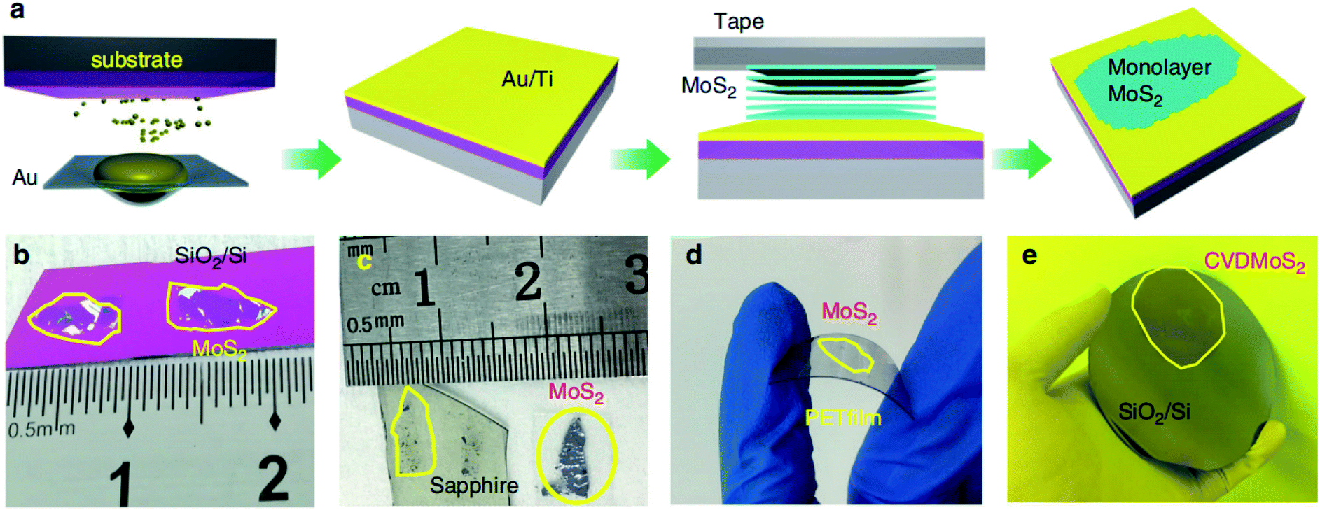 | ||
| Fig. 1 Mechanical exfoliation of different monolayer materials with macroscopic size. (a) Schematic of the exfoliation process. (b–d) Optical images of exfoliated MoS2 on SiO2/Si, sapphire, and plastic film. (e) 2-inch CVD-grown monolayer MoS2 film transferred onto a 4-inch SiO2/Si substrate.30 Reproduced with permission from ref. 30, copyright 2020 Springer Nature. | ||
2.2 CVD method
In the traditional CVD synthesis of 2D MoS2, the solid-state precursors of MoO3 powder and sulfur (S) powder were first evaporated into gaseous states and then reacted with each other in a low-pressure chamber, and MoS2 nuclei formed and gradually enlarged into grains with the aid of carrier-gas flow on the downstream substrates. To achieve large-area continuous monolayer MoS2 films, many efforts have been devoted for improving the CVD synthesis of 2D MoS2, as shown in Fig. 2.31–41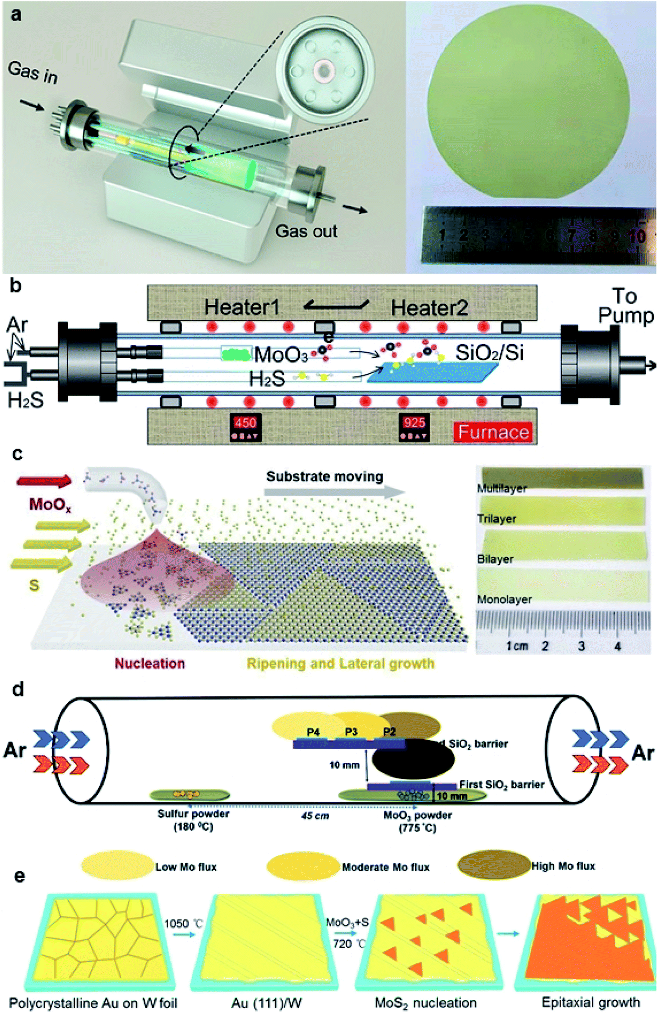 | ||
| Fig. 2 (a) Schematic diagram of the multisource CVD setup and the photograph of a 4-inch sapphire wafer uniformly covered by the monolayer MoS2 film;33 reproduced with permission from ref. 33, copyright 2020 American Chemical Society. (b) Schematic illustration of a homemade two-temperature zone CVD setup and the as-synthesized monolayer MoS2 film;36 reproduced with permission from ref. 36, copyright 2020 IOP Publishing, Ltd. (c) Schematic diagram of substrate-moving atmospheric pressure CVD and the photograph of large-scale MoS2 films;34 reproduced with permission from ref. 34, copyright 2019 IOP Publishing, Ltd. (d) Schematic of the experimental setup showing the side-view geometry of the stair-case-like barrier with different substrate positions and the images for the MoS2 sample were acquired from P2;35 reproduced with permission from ref. 35, copyright 2020 The Royal Society of Chemistry. (e) Schematic illustration of Au(111) formation and the MoS2 growth process, and the photograph of a CVD-grown MoS2 monolayer on the Au(111)/W foil substrate (area ∼3 × 3 cm2).37 Reproduced with permission from ref. 37, copyright 2020 American Chemical Society. | ||
One strategy is to overcome the CVD setup limitations. Yu et al.31 reported a three-temperature-zone CVD system that employs independent carrier gas pathways for sulfur and MoO3 sources to successfully fabricate 2-inch wafer-scale uniform monolayer MoS2 films on sapphire. During the growth, the temperatures for the sulfur source, MoO3 source, and wafer substrate are 115, 930, and 530 °C, respectively, with a typical growth duration of 40 min. Xu et al.32 reported an improved wafer-scale growth of continuous MoS2 film based on atmospheric pressure within a two-temperature-zone CVD setup. As low pressure of 300 Pa can effectively promote the evaporation rate and provide a uniform concentration of the gaseous precursor in the tube to increase the lateral growth rate; thus, a uniform and continuous monolayer MoS2 film can be achieved by increasing the sulfurization time to 15 min. Recently, Wang et al.33 realized the epitaxy of highly oriented and large-domain monolayer MoS2 films at a 4-inch wafer scale via a facile multisource CVD growth method. In this setup, MoO3 sources are evenly loaded within the six minitubes and the S source is loaded within the center minitubes. The carrier gases for S and MoO3 sources are independently delivered through the minitubes. This multisource design provides homogeneous cross-sectional source supply, leading to uniform growth with only 0° and 60° oriented domains and domain size >180 μm. He et al.34 demonstrated a layer-by-layer scalable growth of MoS2 films on a moving sapphire substrate by local-feeding atmospheric-pressure CVD. By the linear moving of the substrate across the cone-shaped diffusion concentration gradient of Mo-containing species and controlling the moving cycles, large-scale growth, uniform monolayer, and few-layer MoS2 with sizes up to ∼4.7 cm × 6 mm can be obtained. The 4-, 7-, and 9-cycle growth corresponding to dwelling times of 8, 14, and 18 min can form complete monolayer, bilayer, and trilayer MoS2 films, respectively. Durairaj et al.35 utilized SiO2 as a mechanical barrier to moderate the Mo flux so as to allow better controllability and high position selectivity for the CVD growth of homogeneous MoS2 monolayers. The barrier offered great control in controlling the Mo precursor vapor concentration at the substrate position, mitigating the secondary and intermediate phases as well as second layer nucleation, thus leading to a continuous monolayer with high surface homogeneity.
Another strategy for improving the CVD synthesis is to adjust the precursor or the substrate. Aside from elemental sulfur powder, hydrogen sulfide (H2S) gas has also proven to be a good sulfur source, which exhibits high vulcanization ability. Liu et al.36 demonstrated that a reproducible and low-cost method for growing wafer-scale (approximately 9.5 × 4.5 cm2) high-quality monolayer MoS2 by using H2S gas as the sulfur source and to stabilize the sulfur vapor pressure during the growth process. In addition, two independent carrier gas pathways for H2S and MoO3 sources were employed to prevent MoO3 poisoning and achieve an improved and stable growth condition. Yang et al.37 reported the epitaxial growth of wafer-scale single-crystal MoS2 monolayers on vicinal Au(111) thin film by a facile ambient-pressure CVD with MoO3 and S as the precursors. Single-crystal Au(111) substrate was obtained by melting and resolidifying the commercial Au foils at a designated temperature (∼1050 °C) for 10 min on cleansed W foils. During the growth, the unidirectional oriented MoS2 domains on the Au(111) film with an area of ∼3 × 3 cm2 started to merge and eventually coalesced into a continuous film after 8 min at ∼720 °C.
Besides these planer substrates, 2D MoS2 can also be synthesized on non-planar substrates. Liao et al.42 firstly proposed single-crystal monolayer MoS2 growth on tapered silica micro/nanofibers (MNFs) and realized photoluminescence (PL) enhancement by high-density oxygen dangling bonds released from the tapered MNFs surface, as shown in Fig. 3. The monolayer MoS2 grown on silica MNF exhibits a PL quantum yield from ∼30% to 1% in a wide pump intensity range from 10−1 to 104 W cm−2 at room-temperature. Due to the taper-drawing process and high-intensity light irradiation, the Si–O bonds of silica can be broken directly and high-density oxygen dangling bonds can be released on the MNFs surface. These reactive oxygen dangling atoms then fill the sulfur vacancies or bridge with neighboring sulfur atoms in monolayer MoS2, forming stable localized sites through electron transfer in MoS2. Thus, the taper-drawing process and high-intensity light irradiation process will reduce the non-radiative carrier-recombination centers and strongly enhance the PL of the monolayer MoS2 in a wide pump dynamic range at room temperature. These unique advantages based on the taper-drawing process enable the direct realization of low-threshold lasing without high-quality factor optical microcavities, which demonstrated great potential in different optical and optoelectronic applications.42–44
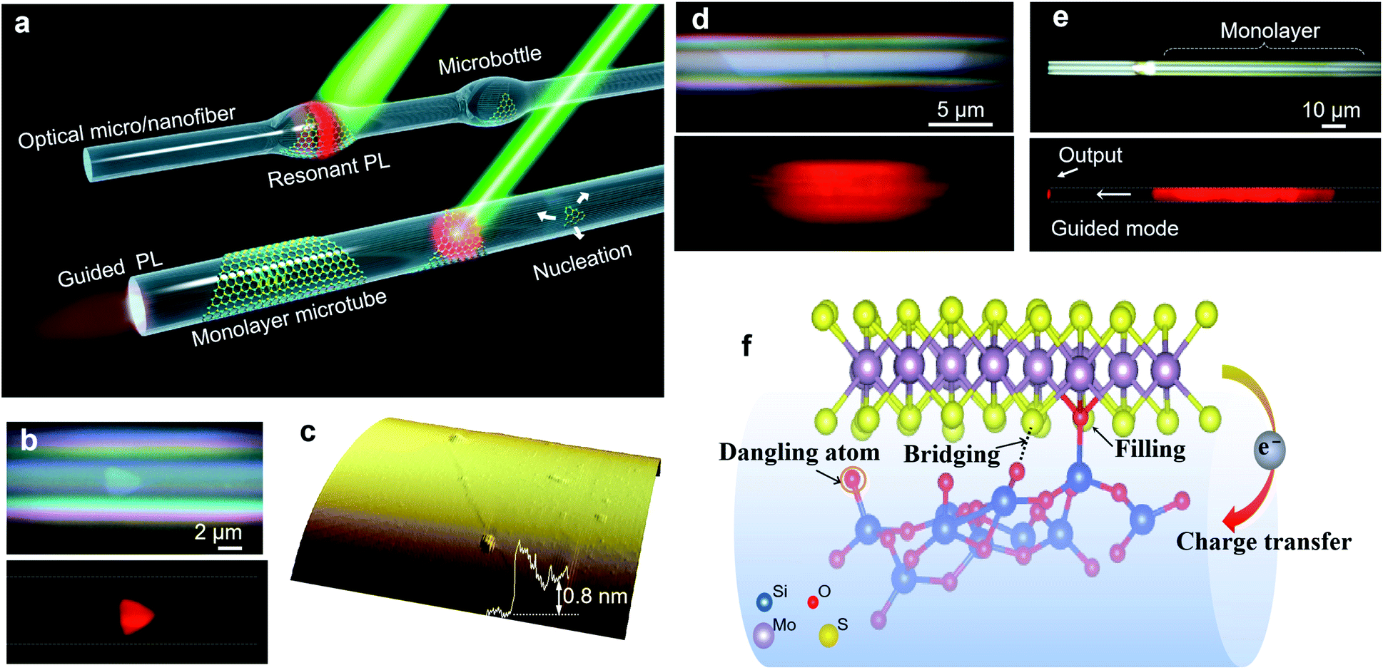 | ||
| Fig. 3 Monolayer MoS2 grown on MNFs. (a) Conceptual illustration of monolayer MoS2 grown on MNFs with uniform diameters and with microbottle structures. A single-crystal triangular domain first nucleates on the MNF surface and then laterally grows into a large-area monolayer structure. A 532 nm CW laser is used to excite the PL emissions. (b) Optical and PL images of a triangular layered MoS2 on a microfiber (Dfiber = 6.1 μm) with (c) a thickness of ∼0.8 nm, as confirmed by an AFM scan. (d) Optical and PL images showing the clean surface and two sharp boundary edges of the MoS2 monolayer/microfiber structure (Dfiber = 5.5 μm). (e) Optical and PL images showing a large-area monolayer/microfiber (Dfiber = 5.4 μm). Some guided emission is emitted at the distal end of the microfiber. (f) The generated oxygen dangling atoms can fill the sulfur vacancies, bridge with neighboring sulfur atoms, and form localized sites by transferring electrons from MoS2, leading to enhanced PL emission.42 Reproduced with permission from ref. 42. | ||
2.3 Thin film sulfurization method
Large-area 2D MoS2 with excellent uniformity can be obtained by sulfuring the deposited Mo or MoOx in a chamber with a sulfur-rich environment. This thin film sulfurization method refers to a two-step process, namely, thin film deposition and the followed sulfurization, which is also classified into two-step CVD methods. As shown in Fig. 4, the Mo precursors can be deposited by various deposition techniques, including electron-beam evaporation, pulsed laser deposition, magnetron sputtering, spin-coating, and ALD. The sulfur source includes S vapor, H2S, and carbon disulfide (CS2).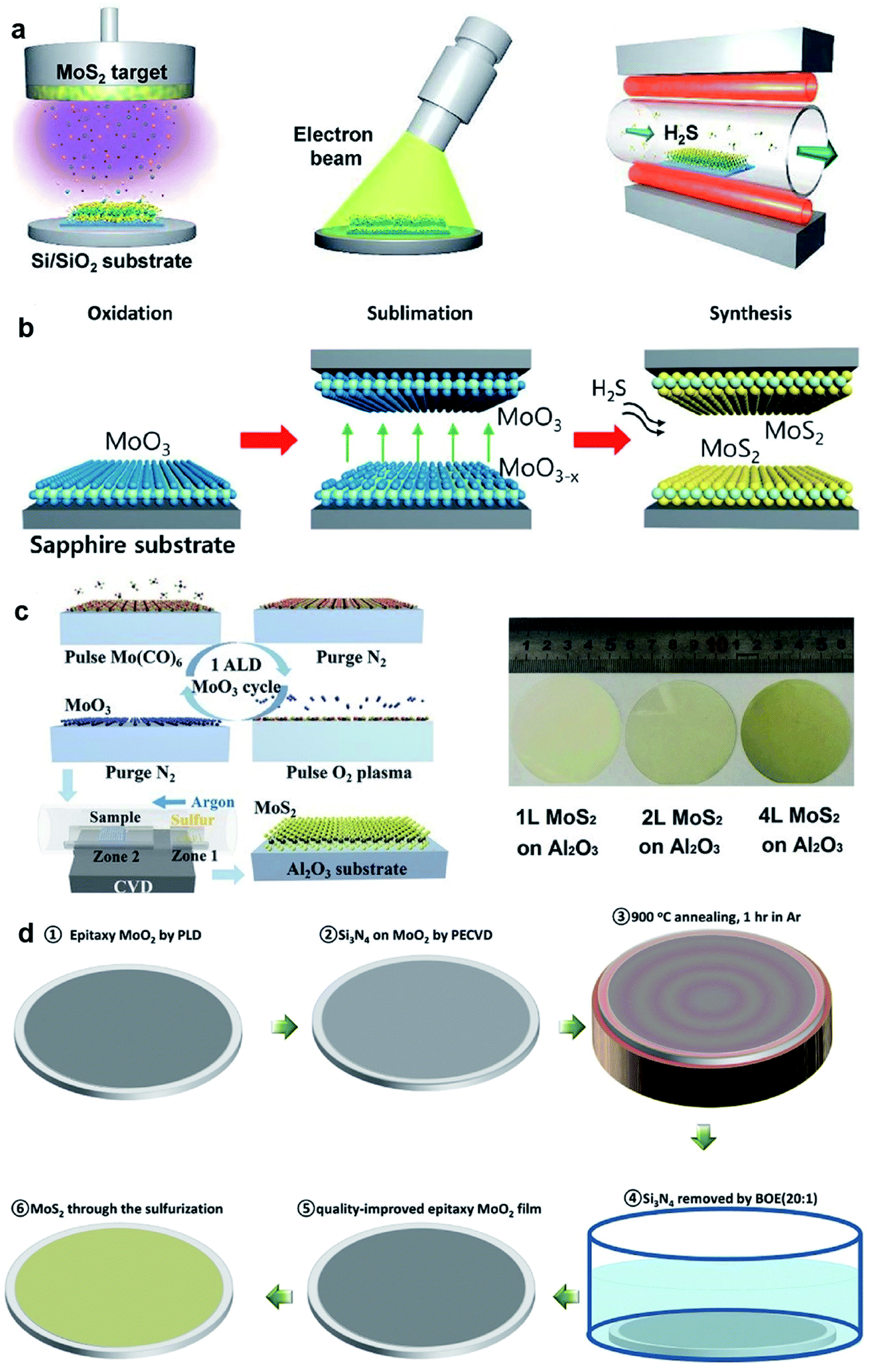 | ||
| Fig. 4 (a) Schematic illustration of the synthetic process of the MoS2 film: sputtering, EBI treatment, and sulfurization;47 reproduced with permission from ref. 47, copyright 2020 American Chemical Society. (b) Schematic illustrations of the reaction sequence of monolayer MoS2via proximity evaporation of the Mo film precursor with the three steps (oxidation, sublimation, and synthesis);49 reproduced with permission from ref. 49, copyright 2020 American Chemical Society. (c) Schematic of one cycle ALD process for the MoO3 film and the sulfurization process for MoS2, and the photo of the MoS2 film on a 2-inch sapphire wafer;52 reproduced with permission from ref. 52, copyright 2017 John Wiley and Sons. (d) Flow diagram showing the synthesis of single-crystal MoS2 films converted from CLAP-treated precursor MoO2 films.51 Reproduced with permission from ref. 51, copyright 2020 John Wiley and Sons. | ||
Kim et al.45 demonstrated wafer-scale 2D MoS2 growth via the sulfurization of transition metals deposited on the SiO2/Si substrates using a home-built chamber. High-quality molybdenum (Mo) was deposited on cleaned SiO2/Si wafers with a typical dimension of 1 × 3 cm2 using an e-beam evaporation system and then placed at the center zone of the CVD furnace for sulfurization by sulfur vapor at 800 °C. Jo et al.46 developed the two-step synthesis of large-area MoS2 thin film by depositing Mo metal films by electron-beam and sulfurizing the Mo film in mixtures of H2S and O2 gas. It was found that the presence of trace levels of O2 accelerates the crystallization of MoS2 and affects the layer orientation, without changing the kinetics of mass transport or the final film composition. Large-area MoS2 films grown on 2-inch wafer, Al, glass, and indium tin oxide (ITO) at 400 °C were realized by this two-step method. Recently, Park et al.47 fabricated MoS2 device arrays constructed on large-dimensional MoS2 films grown using a radio-frequency (RF) magnetron sputtering deposition method combined with post-treatment processes. High-quality centimeter-scale trilayer MoS2 was achieved by sputtering, EBI, and sulfurization. The post-treatments that rearrange the atoms in the MoS2 films can result in an improvement of the MoS2 crystallinity. Almeida et al.48 presented wafer-scale MoS2 growth at arbitrary integer layer number by a technique based on the decomposition of CS2 on a hot Mo filament. As CS2 molecules decompose at the Mo filaments, MoSx precursors evolve, evaporate from the rods, and deposit onto the substrate at 650 °C, where they obtain stoichiometric sulfur contents from the environmental CS2 and form into extended islands or evaporate again. Since the hue value of light from the hot Mo filaments reflected from the wafer substrate changes as the film grows layer by layer, the concomitant measurement of this hue was employed to control the growth process, which allows the precise targeting of any integer layer number.
Besides Mo films, oxidized Mo film is also a precursor source in the sulfurization method. Choi et al.49 synthesized the 2-inch-scale monolayer MoS2 film using an atmospheric pressure reaction process as the result of the reaction between the oxidized Mo and gaseous H2S at a peak temperature of 780 °C. The growth is based on a unique reaction mechanism due to the self-limiting precursor source in a proximity reaction environment with a distance of only ∼0.5 mm from the reaction zone, which provides a unique advantage of uniformity with the self-limiting reaction due to the limited MoO3−x supply. Xu et al.50 realized high-quality MoS2 synthesis over 2-inch wafers through the two-step vapor-solid phase reaction (VSPR) process using MoO2 as the precursor. The epitaxial MoO2 film was firstly deposited on 2-inch wafers by pulsed laser deposition (PLD), then loaded into a tube furnace and annealed in a mixture of Ar and S at 900 °C for 1 h at low pressure, resulting in 2D epitaxial MoS2 films. This quasi-single-crystalline MoS2 film deposited over the 2-inch wafer was ∼3 nm in thickness and can be successfully transferred onto different substrates. Xu et al.51 introduced a new capping layer annealing process (CLAP) to improve the crystalline quality of the as-deposited MoO2 films and minimized its defects in the synthesis of single-crystalline MoS2 films on 2-inch wafers. The epitaxial MoO2 sample was covered with a protective capping layer, such as SiO2 or Si3N4 with a thickness of 50 nm, and then annealed in the PLD chamber at 900 °C for 1 h. After annealing, the capping layer on MoO2 can be totally removed by buffered oxide etching (20![[thin space (1/6-em)]](https://www.rsc.org/images/entities/char_2009.gif) :1) solution. Through the sulfurization of the CLAP-treated epitaxial MoO2 film in a CVD system with sulfur powder source, wafer-scale single-crystalline MoS2 films were obtained without texture. The MoO3 films with desired thickness deposited by ALD is a good candidate for the Mo source in the thin film sulfurization method. Shi et al.52 demonstrated the two-step growth of MoS2 on sapphire substrates by depositing the MoO3 film by ALD using Mo(CO)6 and oxygen plasma as the precursors. The MoO3 film was sulfurized at 500 °C for 20 min, and followed by 20 min annealing at 900 °C in the sulfur vapor to improve the crystallinity of MoS2.
:1) solution. Through the sulfurization of the CLAP-treated epitaxial MoO2 film in a CVD system with sulfur powder source, wafer-scale single-crystalline MoS2 films were obtained without texture. The MoO3 films with desired thickness deposited by ALD is a good candidate for the Mo source in the thin film sulfurization method. Shi et al.52 demonstrated the two-step growth of MoS2 on sapphire substrates by depositing the MoO3 film by ALD using Mo(CO)6 and oxygen plasma as the precursors. The MoO3 film was sulfurized at 500 °C for 20 min, and followed by 20 min annealing at 900 °C in the sulfur vapor to improve the crystallinity of MoS2.
2.4 MOCVD method
The MOCVD technique using metal–organic sources (as shown in Fig. 5), such as Mo(CO)6 and (C2H5)2S, is generally favorable due to highly uniform and accurately layer-controlled, thus avoiding the need for post-deposition treatment and benefiting large-area MoS2 synthesis.53–55 Mun et al.21 reported the kinetics-controlled low-temperature MOCVD method for the direct growth of spatially homogeneous 2D MoS2 film on a polyimide (PI) substrate at a record low process temperature of 250 °C with the precursors of Mo(CO)6 and high-purity H2S. As an alkali-metal catalyst, sodium chloride (NaCl) was precisely controlled in the MOCVD reactor along with the growth substrate. It takes 8 h to successfully obtained 4-inch scale monolayer MoS2 film on PI at 250 °C by the precise and continuous feeding of the alkali-metal catalyst during the MOCVD process. The fabricated flexible MoS2-FET based on directly grown MoS2 demonstrate the excellent stability of the electrical properties following a 1000-cycle bending test with a 1 mm radius. Kalanyan et al.53 presented MoS2 film growth by pulsed MOCVD in a single-wafer reactor using the precursors of (NtBu)2(NMe2)2Mo and Et2S2. Each reaction cycle consisted of 1.5 s co-injections of (NtBu)2(NMe2)2Mo centered on 2 s injections of Et2S2 and then the reactor was purged with 400 sccm Ar for 4 s, resulting in a 6 s cycle time. Pulsed injections of the precursor vapors facilitated excellent control over the film thickness with a growth rate of 0.12 nm/pulse. The layered wafer-scale MoS2 films with thickness from ∼1 nm to ∼25 nm on the SiO2/Si substrates can be achieved at comparatively low reaction temperatures of 591 °C at short deposition times, from tens of seconds to several minutes. Shinde et al.54 proposed a gas-phase CVD approach for the synthesis of atomically thin MoS2 films over 2-inch sapphire wafers with suitable precursors of (NtBu)2(NMe2)2Mo and hydrogen sulfide (H2S). A graphite susceptor was designed for handling a 2-inch wafer facing at a 15° angle to the Ar gas flow. The homogeneous MoS2 films was obtained at 850 °C under 10 Torr with an H2S flow of 3 sccm. In this approach, the growth rate of continuous MoS2 was found to be 1 monolayer (S–Mo–S) per 4 min. Recently, Shinde et al.55 also realized the rapid and large-scale fabrication of the MoS2 layers directly on SiO2/Si (3.5 × 3.5 cm2) using (NtBu)2(NMe2)2Mo and H2S via gas-phase CVD. The seamless growth process allowed the deposition of monolayer MoS2 films in 4 min with excellent spatial homogeneity and optical quality.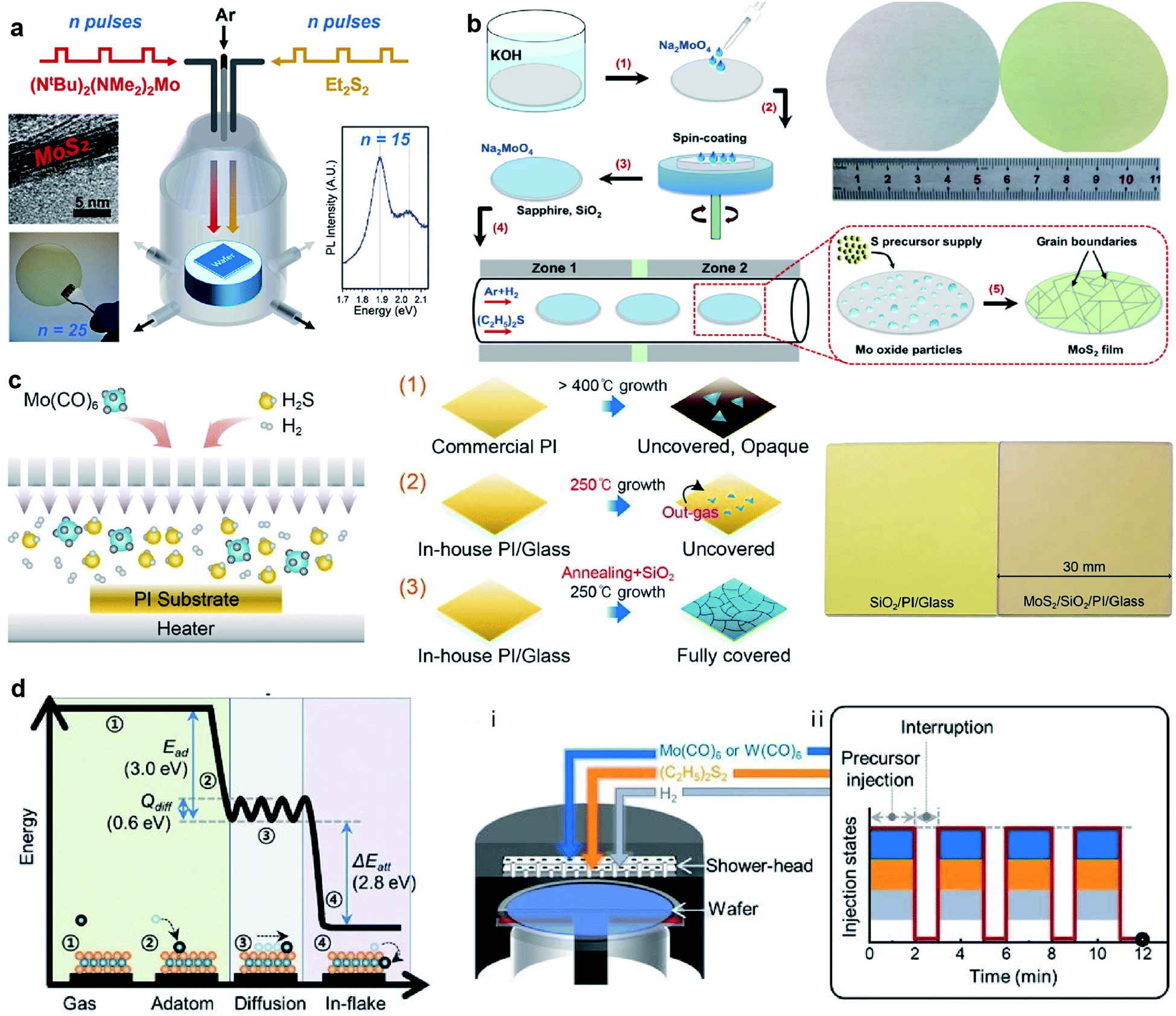 | ||
| Fig. 5 (a) Schematic of pulsed MOCVD growth for 2H-MoS2 in a single-wafer reactor geometry via pulsed injections of (NtBu)2(NMe2)2Mo and Et2S2.53 Reproduced with permission from ref. 53, copyright 2017 American Chemical Society. (b) Schematic illustration of wafer-scale MoS2 film growth process and photos of the 2-inch wafers of clean sapphire substrate (left) and the as-grown MoS2/sapphire (right).56 Inset: The proposed mechanism for MoS2 growth on the substrates. Reproduced with permission from ref. 56, copyright 2019 Springer Nature. (c) Schematic of the direct growth process of MoS2 on the PI substrate: (1) PI is changed to opaque and sparse MoS2 islands are grown; (2) the growth of MoS2 at 250 °C. (3) The heat-annealing and capping procedures prevent the outgassing phenomenon and further absorption in the ambient environment, forming fully-covered MoS2.21 Reproduced with permission from ref. 21, copyright 2019 American Chemical Society. (d) Calculated reaction energy diagram of Mo adsorbed on the basal plane of MoS2 and the schematic illustration of (i) the reactor geometry and (ii) injection sequence of the precursors for growing wafer-scale monolayer TMD by pulsed MOCVD.57 Reproduced with permission from ref. 57, copyright 2020 John Wiley and Sons. | ||
Cun et al.56 developed the wafer-scale growth of high-quality monolayer MoS2 on single crystalline sapphire and SiO2 substrates at the 2-inch wafer scale by a facile MOCVD with a spin-coated Mo precursor and a non-toxic sulfur precursor. An aqueous solution of sodium molybdate (Na2MoO4) was provided as the Mo precursor by spin-coating on the substrates prior to the growth, and the amount of Mo can be controlled by the concentration of Na2MoO4 and the spin-coating speed. The single sulfur precursor was supplied by the non-toxic liquid organic compound diethyl sulphide (C2H5)2S, which is stored in a stainless-steel bubbler and connected to the quartz tube with a mass flow controller (MFC) to precisely control the amount of the required sulfur precursor during the growth. The obtained wafer-scale MoS2 films exhibit crystallinity and good electrical performance.
Seol et al.57 realized high-throughput production of 6-inch wafer-scale monolayer MoS2 and WS2via a pulsed MOCVD technique. A scalable shower-head-type cold-wall reactor system was used and the gas-phase precursors included molybdenum hexacarbonyl (Mo(CO)6), (C2H5)2S, and H2. Each reaction cycle consisted of 2 min of co-injection of all the precursors, followed by interrupting the precursors' supply and purging with N2 for 1 min. Periodic interruption of the precursor supply allowed the successful regulation of secondary nucleation even under high growth rates; as a result, wafer-scale monolayer MoS2 and WS2 were obtained within 12 min on 6-inch quartz substrates. Moreover, the as-grown TMD films show excellent spatial homogeneity and well-stitched grain boundaries, enabling facile transfer to various target substrates without degradation.
2.5 Vapor–liquid–solid (VLS) method
The reported CVD of 2D MoS2 is generally conducted through a typical vapor–solid–solid mechanism or a vapor–gas–solid mechanism using powdered precursors (MoO3 and S) or mixed precursors (MoO3 powders and H2S gas), respectively. The vapor–liquid–solid (VLS) growth method often involves molten precursors (e.g., non-volatile Na2MoO4) at growth temperatures higher than their melting points, which presents great promise in large-area MoS2 synthesis with large single crystals for electronics.58–60Recently, Li et al.59 demonstrated the VLS growth of uniform monolayer MoS2 flakes on 4-inch SiO2/Si wafers and continuous MoS2 films with the grain size exceeding 100 μm on 2-inch sapphire substrates using non-volatile precursors. Na2MoO4 particles were first dispersed on the growth substrate by spin-coating its aqueous solution. Then, Na2MoO4 on the substrates was loaded in the tube furnace and started to melt into a liquid, wetting the substrate surface when the temperature was higher than its melting point (687 °C). Sulfur vapor dissolves into the Na–Mo–O droplets, and the MoS2 monolayer nucleated and grew from the sulfur over-saturated Na–Mo–O–S liquid on the substrate at 750 °C. Moreover, the Na2MoO4 particles can be patterned on the substrate with the aid of the photolithography process; patterned MoS2 monolayers with desired sites were grown on the substrate after sulfurization.
Chang et al.60 also utilized a self-capping vapor–liquid–solid (SCVLS) reaction for the growth of large single crystals and full-coverage TMD films. As shown in Fig. 6, a solid precursor comprising ultra-thin MoO3, SiO2, and NaF layers was used for the controllable eutectic reaction of MoO3 and NaF at high temperature. Firstly, MoO3 vapor broke the SiO2 layer, diffused upward, and reacted with the NaF layer at a temperature higher than 500 °C to form liquid-phase Na2Mo2O7 and gas-phase MoO2F2. Simultaneously, the consumption of NaF generated holes and pathways in the NaF layer, which allowed Na2Mo2O7 and MoO2F2 to gradually rise to the top surface of the NaF. The as-formed eutectic liquid (Na2Mo2O7) rose to the surface and was sulfurized into MoS2 seeds, which acted as a self-capping layer and redirected the rising liquid into a horizontal direction. The residual liquid was continuously pushed along the growth direction and eventually sulfurized to form new MoS2 at the edge of the MoS2 seeds, thus making millimeter-sized MoS2 single crystals formed on a c-plane sapphire.
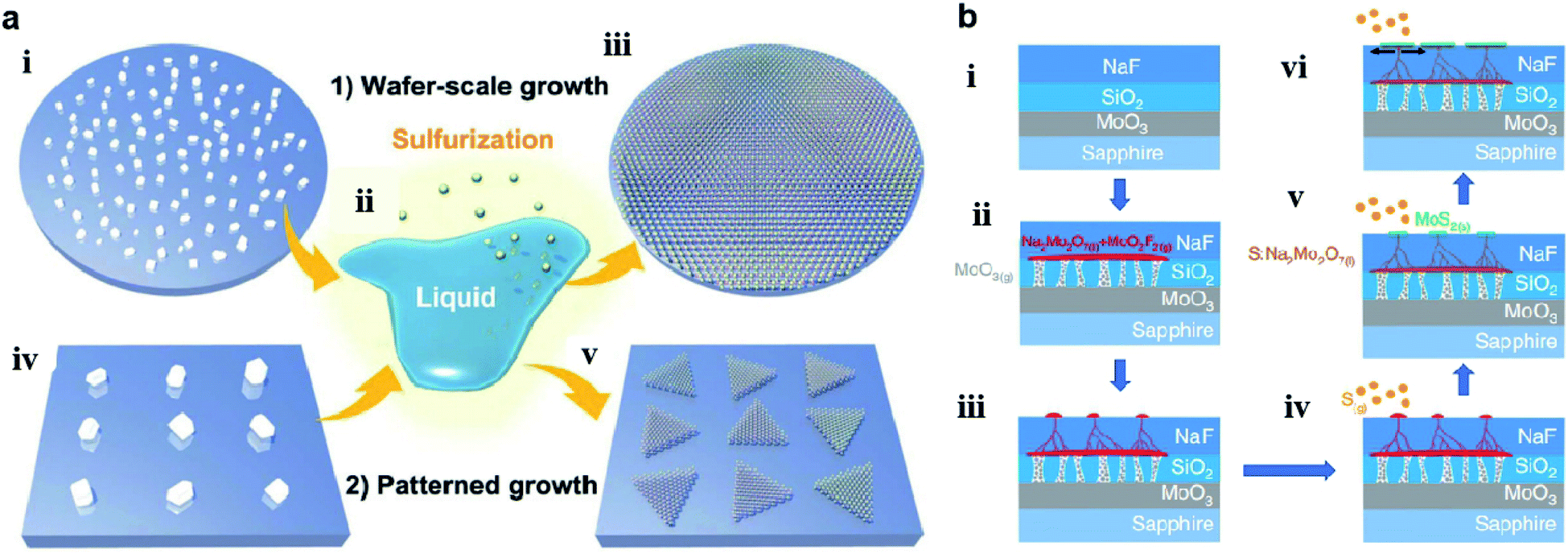 | ||
| Fig. 6 (a) Schematics of wafer-scale and patterned growth of MoS2 monolayers via the VLS method: (i) dispersed Na2MoO4 particles on sapphire wafer; (ii) molten Na2MoO4 droplet starts to wet the substrate surface; (iii) sulfurization of the molten Na2MoO4 droplets leads to the nucleation and growth of the VLS-MoS2 film on the whole wafer; (iv) patterned Na2MoO4 particles on the growth substrate with the aid of photolithography; (v) patterned growth of monolayer VLS-MoS2 flakes by the sulfurization of the site-specific non-volatile Na2MoO4 droplets.59 Reproduced with permission from ref. 59, copyright 2019 The Royal Society of Chemistry. (b) Schematics of the SCVLS growth mechanism and the grown MoS2: (i) structure of the solid precursor; (ii) MoO3 vaporized and penetrated through the SiO2 diffusion membrane. MoO3 and NaF reacted to form liquid-phase Na2Mo2O7 (colored in red) at the growth temperature; (iii): the liquid precursor gradually rose to the NaF matrix surface; (iv) sulfur vapor started to dissolve into the Na2Mo2O7 liquid. (v) Liquid precursor sulfurized into the MoS2 seed layer; (vi) capped by the MoS2.60 Reproduced with permission from ref. 60, copyright 2020 Springer Nature. | ||
2.6 ALD method
ALD exhibits advantages in the precise control of the film thickness, uniformity, and homogeneity over large-scale wafers due to the self-limiting growth mechanism. MoS2 films with desired thickness can be obtained by varying the ALD cycles. The ALD procedure combines precursor exposure, purging, reactant exposure, and a final purging into a single cycle. The layers of the ALD MoS2 films can be determined by the deposition temperatures and the ALD cycles. Large-area MoS2 directly onto SiO2/Si substrates have been achieved through the ALD method using molybdenum pentachloride (MoCl5) and H2S as the precursor and the reactant, respectively.61 In different reports, the ALD growth temperatures of MoS2 ranges from 350 °C to 900 °C.61–64 Another well-investigated precursor pair for ALD MoS2 is Mo(CO)6/H2S. This ALD process features the high vapor pressure of Mo(CO)6 at room temperature and relatively low growth temperature. Jang et al.65 reported MoS2 film grown uniformly, reliably, and directly on a 4-inch wafer by ALD using an Mo(CO)6 precursor and H2S plasma as the precursor and reactant without a post-sulfurization process. The growth rate of MoS2 on SiO2/Si was approximately 0.05 nm per cycle and the deposition temperature ranged from 175 to 225 °C. Pyeon et al.66 presented wafer-scale synthesis of MoS2 layers on a 4-inch SiO2/Si wafer with precise thickness controllability and excellent uniformity by ALD in the narrow ALD window of 155–175 °C, with Mo(CO)6 and H2S as the Mo and S precursors, respectively. Post-annealing in the range of 500–900 °C under an H2S atmosphere efficiently improved the film properties, including the crystallinity and chemical composition. Extremely uniform film growth was achieved even on a 4-inch SiO2/Si wafer. The growth temperature can be reduced in an ALD process using tetrakis(dimethylamido)-molybdenum(IV) (TDMA-Mo, Mo(NMe2)4) and H2S as the precursors with an ALD growth rate of 1.2 Å per cycle at 60 °C.67 Then, the obtained amorphous MoS2 was treated at 1000 °C under sulfur vapor to improve the crystallinity. Recently, Liu et al.68 developed thickness-controlled MoS2 synthesis using MoCl5 and hexamethyldisilathiane (HMDST) as the ALD precursors; the films were uniformly deposited on a sapphire and SiO2/Si substrate after different ALD cycles from 20 to 90. As shown in Fig. 7, the thickness of the as-grown MoS2 film after 50 ALD cycles was measured for 2.9 nm on sapphire and ∼5 nm on the SiO2/Si wafer with high uniformity. | ||
| Fig. 7 ALD-grown MoS2 on the sapphire substrate. (a) Schematic of our ALD-grown MoS2 films, with MoCl5 and hexamethyldisilathiane (HMDST) as the precursors. (b) Images of sapphire substrate; 20, 30, 40, 50, 60, 70, and 90 cycles of ALD-grown MoS2 on sapphire. (c) 3D AFM image of ALD-grown MoS2 film on a 10 μm × 10 μm area, with the roughness RMS of this region being 0.479 nm. (d) TEM images of an annealed 50-cycle MoS2 film of 2.9 nm thickness on the sapphire substrate.68 Reproduced with permission from ref. 68, copyright 2020 Springer Nature. | ||
2.7 Thermolysis of thiosalts
MoS2 synthesis by the thermolysis of thiosalts is based on the thermal decomposition of ammonium thiomolybdates (NH4)2MoS4 in a specific environment, which results in the conversion of (NH4)2MoS4 to MoS2 at a higher temperature. The precursor solution of (NH4)2MoS4 can be deposited on different substrates and highly crystalline centimeter-scale MoS2 can be synthesized after thermal decomposition in a N2 or sulfur-rich atmosphere.69–72 Lim et al.71 reported large-area MoS2 layers by the simple coating of single source precursor with subsequent roll-to-roll-based thermal decomposition with N2 at 600 °C under 1.8 Torr pressure. An (NH4)2MoS4 solution was bar-coated onto a Ni foil and subsequently thermally decomposed using the roll-to-roll process, resulting in 50 cm long MoS2 layers synthesized on Ni foils with excellent long-range uniformity and optimum stoichiometry. The number of MoS2 layers can be simply adjusted by optimizing the concentration of (NH4)2MoS4 and the solvent conditions. Park et al.72 introduced a direct and rapid method for the layer-selective synthesis of patterned MoS2 at the wafer-scale using a pulsed laser annealing system (λ = 1.06 μm, pulse duration ∼100 ps) in ambient conditions. The (NH4)2MoS4 precursor was spin-coated on a Si/SiO2 wafer and annealed at 150 °C for 3 min to evaporate the residual solvents. Then, a pulsed fiber laser was used to induce a local photothermal reaction under sulfur-rich conditions to thermally decompose into MoS2. The heat treatment area was precisely defined and the precursor layer in the non-treated area was simply removed by the DMF solvent, leaving a patterned MoS2 film. Fig. 8(c) and (d) provide the mechanism of selective conversion of (NH4)2MoS4 precursors into MoS2. Moreover, the ultrafast and selective synthesis of individual patterned MoS2, WS2 layers, and stacked WS2/MoS2 heterojunction structure can be directly realized on a 4-inch wafer.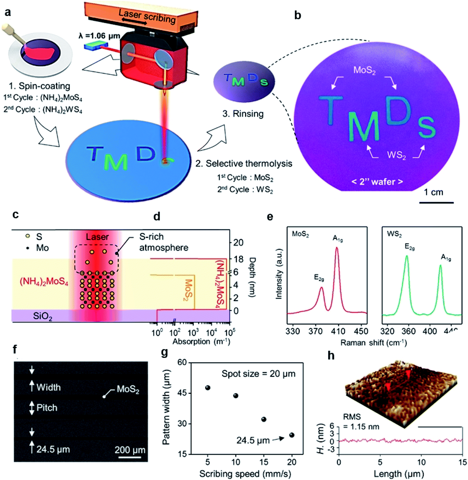 | ||
| Fig. 8 Layer-selective synthesis of MoS2 and WS2. (a) Schematic illustration of the selective synthesis of MoS2- and WS2-based homostructures. (b) Photograph of patterned MoS2 and WS2 on the 2-inch SiO2/Si substrate. (c and d) Synthetic mechanism of MoS2 and the absorption coefficient profile of each layer. (e) Raman spectra of synthesized MoS2 and WS2. (f) SEM image of the line-patterned MoS2 with different scribing speeds. (g) Pattern width and pitch variation as a function of the scribbling speed. (h) Three-dimensional surface morphology of MoS2.72 Reproduced with permission from ref. 72, copyright 2020 American Chemical Society. | ||
3. Application in basic MoS2-FET
The downscaling trend of integrated electronics based on silicon-based micro-fabrication processes lead to continuing demands for minimizing the channel thickness. 2D MoS2 with atomic thickness is considered as one of the most promising candidates for advanced electronics with minimum channel thickness. The wafer-scale 2D MoS2 films synthesized from different methods can be transferred and integrated onto a variety of substrates by PMMA and PDMS, demonstrating many important applications in electronic and optoelectronic devices.11–13,31 Thus, the fabrication process of wafer-scale MoS2-based devices can be more compatible with the traditional CMOS fabrication process. In order to be compatible with typical transistor requirements for electronic applications, many investigations have focused on developing wafer-scale monolayer MoS2 and high-performance MoS2-FET.11–13 Generally, a typical 2D MoS2-FET involves three terminals (namely gate, drain and source), with a basic configuration consisting monolayer or few-layer MoS2 channel, electrical contacts for the source and drain, dielectric layer, and gate electrode. Jing et al.73 summarized the different 2D FET configurations reported in the previous study for research purposes: (i) back-gated FET with Si as the gate; (ii) back-gated FET with a manufactured metal gate electrode; (iii) top-gated FET; (iv) dual gate FET structure with an Si back gate, (v) dual-gated FET with a patterned back gate; (vi) liquid-gated FET structure. Considering the Schottky barrier and interface scattering effect, the dielectric layer is known to be a key factor for all these configurations, which should be compatible with the 2D channel to suppress extrinsic scattering. Commonly used dielectric layers include inorganic materials and some polymers, such as SiO2, Al2O3, HfO2, ZrO2, PVDF, PMMA, and CaF2.74–81 Few-layer graphene, h-BN and MoSe2 are also considered as dielectrics to improve the field effect mobility in MoS2-FET.82–84 Another key issue is contact and channel engineering in the FET device fabrication based on large-area 2D MoS2 films. The terminals of the drain and the source refer to the metal electrode, such as Au, Cr/Au, Ti/Au, Pd/Au, Ni/Au, and Cr/Pt, which is deposited and patterned via electron beam evaporation and the lithography process. Due to the Schottky barrier and Fermi level pinning at the metal/semiconductor interface, different investigations in MoS2-FET have been made to minimize the contact resistance and realize near-ohmic contacts by choosing appropriate work function metals, creating an ultra-clean interface, inserting a buffer layer, etc.85–91 In this regard, extensive efforts have been devoted to investigate 2D MoS2-FET based on wafer-scale monolayer or few-layer MoS2 with different device configurations and dielectric layers.3.1 Configurations and fabrications
Similar to that of traditional silicon-based FET, different configurations of FET based on 2D MoS2 have been studied in recent years. The most common configurations include: (1) back-gated MoS2-FET, (2) top-gated MoS2-FET, (3) dual-gated MoS2-FET. These MoS2-FET devices can be fabricated through a series of general processes with different processing sequences, including MoS2 patterning, dielectric layer deposition, metal electrode deposition, and patterning. Most MoS2 channels are patterned by controlled plasma etching or the lithographic method after MoS2 synthesis or transfer, while other MoS2 channels can be realized from the patterned thin-film Mo precursor after sulfurization.76,91–97 The dielectric layer of Al2O3, HfO2, and ZrO2 are usually deposited by ALD, while PVDF and PMMA are prepared by the spin-coating method. The metal electrodes can be defined and deposited by e-beam evaporation after the photolithography process or e-beam evaporation with shadow masks.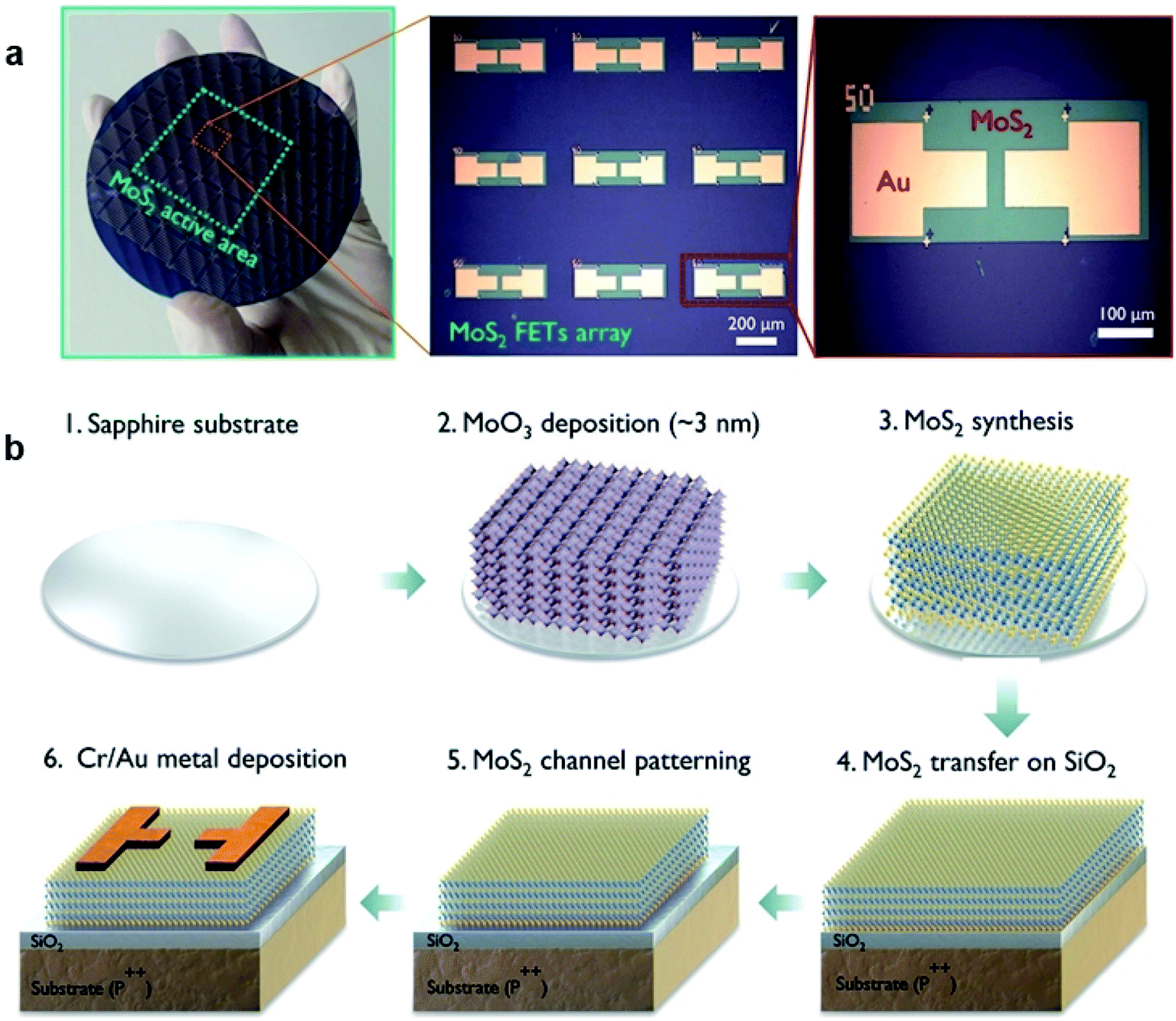 | ||
| Fig. 9 (a) Optical image of the 2D MoS2-FET array devices integrated on a 4-inch SiO2/Si wafer and (b) the sequence of the fabrication process for MoS2 array devices.75 Reproduced with permission from ref. 75, copyright 2017 American Chemical Society. | ||
Back-gated FET with patterned metal or semiconducting gate electrode is another configuration used in MoS2-FET. Seol et al.55 fabricated back-gate MoS2-FETs on a 6-inch wafer with Ti/Au as the back-gate contact and ALD-Al2O3 as the gate dielectric. The as-grown MoS2 film was transferred by PMMA and patterned using photolithography and O2 plasma etching after the deposition of Ti/Au and Al2O3. Wei et al.87 developed a flexible back-gated MoS2-FET fabricated on low-cost polyethylene terephthalate (PET) substrates by 2D MoS2 and dielectric ceramic Bi2MgNb2O9 (BMN). Recently, Li et al.13 reported flexible MoS2-FET arrays on the PET substrate with an improved device density of 1518 per cm2. The wafer-scale MoS2 monolayers grown on sapphire were transferred onto PET substrates with pre-deposited ITO and Al2O3, which serve as the back-gate electrode and dielectric layer. It is also demonstrated that Au/Ti/Au rather than Ti/Au is an excellent contact structure to reduce contact resistance in the monolayer MoS2 devices. Lan et al.88 demonstrated both N-type and P-type MoS2-FET by directly growing MoS2 on the fin oxide structure by the CVD method. The fin oxide structures selectively-implanted Si contacts lead to N-type and P-type MoS2 film growth on a wafer/chip, which can be compatible with the Si-based fabrication process. The SiO2 interfacial layer and HfO2 high-k dielectric were deposited on CVD-grown MoS2 by ALD, followed by metal-gate deposition. The Fin-FET based on MoS2 synthesized from the P+–Si and N+–Si contact presented P-type and N-type performance, respectively, which can be integrated as a complementary MoS2 inverter for basic integrated circuit complementary device applications.
Zhang et al.76 successfully fabricated top-gated MoS2-FET arrays based on wafer-scale continuous MoS2 film using wafer-scale Si shadow masks (Si-SMs) with customized patterns. Metal deposition and plasma etching by the Si-SMs exhibit well-defined patterns with sharp edges. As shown in Fig. 10, top-gated MoS2-FET arrays were fabricated using two different processing strategies assisted by the Si-SMs: ‘etching-last’ and ‘channel-first’. For the ‘etching-last’ strategy, the metal contacts were deposited with the Si-SMs at the beginning, followed by the plasma etch to isolate a continuous film with Si-SM as the protective layer. For the ‘channel-first’ method, a layer of Mo metal defined by Si-SM was deposited on the sapphire substrate. Then, the patterned Mo was subsequently sulfurized in a sulfur-rich atmosphere at 900 °C to form a patterned poly-crystalline MoS2 film. The MoS2-FET arrays can be obtained after dielectric growth and top gate deposition, without suffering from photoresist residue and long-time immersion in the photoresist remover.
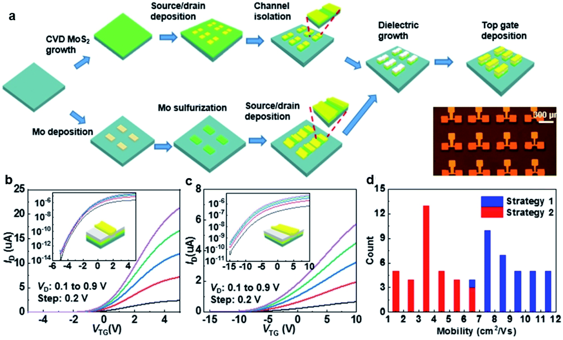 | ||
| Fig. 10 (a) Schematic illustration of strategy 1: ‘etching-last’ and strategy 2: ‘channel-first’. The bottom right corner shows an optical image of the as-fabricated MoS2-FET device arrays. The transfer characteristics of the top-gated transistor fabricated using (b) ‘etching-last’ and (c) ‘channel-first’ at different Vds. The insets show the corresponding transfer curves on a log-scale. (d) Histograms of the effective mobility of the CVD arrays fabricated with the two strategies.76 Reproduced with permission from ref. 76, copyright 2020 IOP Publishing, Ltd. | ||
Wang et al.33 built top-gated FET with a high-κ HfO2 directly fabricated from the CVD-grown monolayer MoS2. The MoS2 active regions for the transistors were defined in a patterning step, followed by a CHF3-based reactive ion etching process. After that, Ti/Au source/drain electrodes were formed by electron beam evaporation, following the patterning step. The gate dielectric of HfO2 was grown by ALD and the top-gate Ti/Au was deposited, followed by a standard lift-off process. Similar to the back-gate FET, P(VDF-TrFE) and PMMA were also reported as the gate dielectric by spin-coating in the top-gated MoS2-FET.79
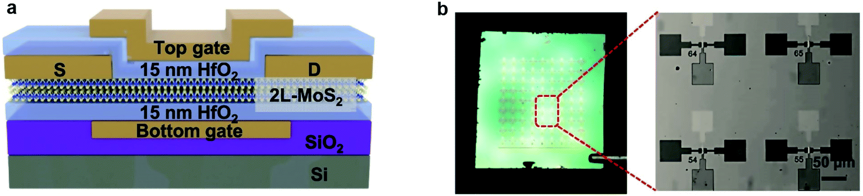 | ||
| Fig. 11 Schematic illustration, optical images, and electrical characteristics of the dual-gated MoS2 device. (a) Cross-sectional schematic of the dual-gated MoS2 device. (b) Photograph of a dual-gated bi-layer MoS2 transistor array on a 1 × 1 cm2 wafer (left) and an optical microscopic image (right) of the zoom-in area at the left.99 Reproduced with permission from ref. 99, copyright 2019 IOP Publishing, Ltd. | ||
3.2 Characterization and performances
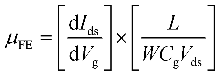
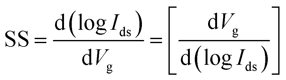
The characterization of synthesized MoS2 films and fabricated MoS2-FETs is essential for both fundamental research and practical application. The basic characterization of 2D MoS2 consists of lateral size, thickness, morphology, PL spectroscopy, and Raman spectroscopy, which can be measured by optical microscopy, atomic force microscopy (AFM), photoluminescence spectrometry, and Raman spectroscopy, as shown in Fig. 7(c), (d) and 8(e), (h). Further information of the 2D MoS2 film, such as grain size, grain boundaries, lattice orientations, phase composition, and structural defect determination, can be inferred from various microscopy techniques, such as scanning tunneling microscopy (STM), high-resolution transmission electron microscopy (HRTEM), and low-energy electron diffraction (LEED). In addition, the X-ray diffraction (XRD) technique, X-ray photoelectron spectroscopy (XPS), and ultraviolet-visible (UV-vis) spectrophotometry were also applied for the investigation of the film quality and the optoelectronic property based on 2D MoS2.The typical characterization of 2D MoS2-FETs refers to the current flowing between the drain and the source (Ids), which can be controlled by tuning the gate voltage (Vg) and the drain–source voltage (Vds). The main figures of merit of an FET are the transfer characteristic (Idsvs. Vg, for a specific Vds) and the output characteristic (Idsvs. Vds, for various Vg). The measurement transfer characteristic (Ids − Vg) and the output characteristic (Ids − Vds) of the 2D MoS2-FET were usually carried out on a semiconductor parameter analyzer (such as Keithley 4200-SCS) at room temperature. From the transfer characteristic, several important operational parameters of the FET can be extracted, such as the current ratio between the ON and OFF states (Ion/Ioff), threshold voltage (Vth), field effect mobility (μFE), and subthreshold slope (SS). The value field effect mobility and subthreshold slope can be evaluated using eqn (1) and (2)
 | (1) |
 | (2) |
Since the performance is directly affected by the MoS2 quality and device configuration, different factors should be considered in 2D MoS2-FETs, such as film thickness, grain size, defect situation, electrode/channel contact resistance, dielectric layer, channel length, and channel width. The improved quality of the wafer-scale MoS2 films with larger grain size and less defects is preferred in MoS2-FET with different configurations. The resistance of the electrode/channel contact caused by the Schottky barrier and Fermi-level pinning at the metal/channel interface can be reduced by the post-annealing process, optimizing the stacked metal electrode, and inserting a buffer layer.85–87,90–92 Since the large dielectric constant of the high-k material contributes to the reduction of the effective size of the Coulomb impurities, different dielectric layers, such as SiO2, HfO2, Al2O3, LiNbO3, CaF2, PMMA, PVDF, h-BN, and graphene, have been utilized as the gate dielectric to improve the mobility of 2D MoS2-FET.75–84 The dielectric layer can also be used on the top of the MoS2 channel, function as the encapsulation layer, and to provide a dielectric environment to improve the device performance and reliability. The performance of different 2D MoS2-FETs based on the monolayer and few-layer MoS2 films are summarized in Table 1.
| MoS2 | Configurations | Dielectrics | L (μm) | μ FE (cm2 V−1 s−1) | I on/Ioff ratio | SS (mV dec−1) | Ref. |
|---|---|---|---|---|---|---|---|
| Monolayer on sapphire by CVD | Top-gated | HfO2 | 3.5 | 0.1–3 | >106 | 130 | 8 |
| 4-Inch monolayer by CVD | ITO back-gated | Al2O3 | 6 | ∼55 | 1010 | 13 | |
| Few-layer by exfoliation | Back-gated | SiO2 | 2 | 167 ± 20 | 14 | ||
| 8-Inch monolayer by MOCVD | Back-gated | SiO2 | 10 | 0.47 | 5.4 × 10⁴ | 18 | |
| 4 inch-scale by MOCVD | Back-gated | SiO2 | 7–12 | 104–107 | 21 | ||
| 6-Inch monolayer by CVD | Back-gated | SiO2 | 1 | 6.3–11.4 | 105–106 | 24 | |
| Monolayer by Au-assisted exfoliation | Top-gated | SiO2 | 22.1–32.7 | ∼107 | 100 | 30 | |
| 2-Inch monolayer by CVD | Back-gated | SiO2 | 30–60 | ∼40 | ∼106 | 31 | |
| 2-Inch continuous by CVD | Top-gated | HfO2 | 10–100 | 70 | 107 | 150 | 32 |
| 4-Inch monolayers by CVD | Back-gated | SiO2 | 10 | ∼70 | ∼109 | 33 | |
| Monolayer by APCVD | Back-gated | Al2O3 | 0.033 | 5.8 × 10⁵ | 34 | ||
| Wafer-scale monolayer by CVD | Back-gated | SiO2 | 20 | 1.2 | 35 | ||
| Monolayers on Au by CVD | Back-gated | SiO2 | 5 | ∼11.2 | 7.7 × 10⁵ | 37 | |
| Continuous monolayer by CVD | Back-gated | SiO2 | 1 | ∼9.8 | 3.1 × 10⁶ | 40 | |
| 2-Inch by PLD and sulfurization | Top-gated | HfO2 | 90 | 8.85 | ∼105 | 50 | |
| Monolayer by MOCVD | Back-gated | SiO2 | 10 | 21.6 | 51 | ||
| Monolayer on 2-inch sapphire | Top-gated | Al2O3 | 15 | ∼0.76 | ∼104 | 52 | |
| 3.5 × 3.5 cm2 monolayer by CVD | Back-gated | SiO2 | 20 | 1.3 × 10⁻² | ∼104 | 8300 | 55 |
| 2-Inch monolayer by MOCVD | Back-gated | SiO2 | 10 | 21.6 | 56 | ||
| Monolayer by MOCVD | Ti/Au back-gated | Al2O3 | 10 | 3.4 ± 0.3 | 107 | 57 | |
| Monolayers by VLS | Back-gated | SiO2 | 21.1 | 107–109 | 59 | ||
| 1.5 × 1.5 cm2 monolayer by VLS | Back-gated | SiO2 | 1.48 | 33 | >108 | 980 | 60 |
| Few-layer on sapphire by ALD | Top-gated | Al2O3 | 25 | 0.56 | 106 | 68 | |
| Continuous monolayer by CVD | Top-gated | Al2O3 | 6.44 | >108 | 76 | ||
| 10 × 10 mm2 monolayer by CVD | Back-gated | HfO2 | 6 | 118 | 108 | 77 | |
| Monolayer and bilayer by CVD | Dual-gated | Y2O3/HfO2 | 10 | 1–9 | >106 | 90 | |
| Monolayer by CVD | Back-gated | SiO2 | 2.87 | 3.2 × 10⁶ | 96 | ||
| Bilayer by CVD | Dual-gated | HfO2 | 10 | 32.5 | ∼800 | 99 |
From Table 1, it can be inferred that the performance of MoS2-FET varies considerably from device to device. Different factors, such MoS2 thickness, device configuration, dielectric choice, channel size, and fabrication process, interact and simultaneously affect the performance of MoS2-FET. Even though the field effect mobility is still behind the highest reported value (167 ± 20 cm2 V−1 s−1) from the exfoliated MoS2,14 the Ion/Ioff ratio and field effect mobility of MoS2-FET based on wafer-scale monolayer MoS2 is encouraging. Considering the complicated fabrication procedures and different repeatability, it is difficult to make simple comparisons between different devices based on the monolayer MoS2 film from different synthetic methods. Overall, more developments are needed for realizing high-performance MoS2-FET with larger mobility, higher Ion/Ioff ratio, steeper subthreshold slope, and better stability. With the development of MoS2 synthesis and MoS2-FET engineering, the improved basic performance of wafer-scale MoS2 devices will render the wafer-scale MoS2 film to be a promising candidate for next-generation electronics, which can be compatible with the traditional silicon-based fabrication process.
4. Toward practical application
Although the charge carrier mobility of 2D MoS2-FET is not directly comparable to that of Si-based devices, the high Ion/Ioff ratios and low stand-by power suggests suitable application for low-power electronics and optoelectronics. To advance one step further from a single FET to a complex device, the explorations of electronic devices and optoelectronic devices based on 2D MoS2, such as N-metal-oxide-semiconductor (NMOS) inverters, logic gate circuits (NAND, NOR, NOT, AND), content-addressable memory (TCAM), and integrated photodetectors, presents great potential application of 2D MoS2-FET for future integrated electronics and flexible optoelectronics.13,68,98,101–1424.1 Logic devices
To build a working logic device, basic requirements are necessary for voltage switching and high frequency operation, such as high Ion/Ioff ratio (>1000) and moderate mobility. In practical applications, different individual MoS2-FET can be integrated with necessary designs for realizing an inverter. Shin et al. realized a logic inverter and NAND gate based on the GaS/MoS2 heterostructure comprising a switching transistor and a load resistor. The upper transistor is the load resistor with the transistor gate connected to the output electrode, while the lower transistor acts as a switch by applying an input signal to the gate.Liu et al.68 realized an inverter from two top-gated MoS2-FETs and constructed several complex logic devices from 3 or 5 MoS2-FETs. The top-gated FETs based on the wafer-scale MoS2 synthesized by the ALD method show a high on/off ratio at 106 and a carrier mobility of 0.56 cm2 (V−1 s−1). An inverter with a fast response was fabricated using two N-type MoS2-FETs (a load FET and a pull-down FET) with a different width of the channel, while the gate electrode of the pull-down FET serves as the input terminal. The NAND and NOR gates with three or five FETs were built successfully based on the load FET and the pull-down FET with channel sizes of L = 5 μm, W = 50 μm, and L = W = 5 μm. Two different input voltages, −5 V and 8 V, correspond with the input state of ‘0’ and ‘1’, respectively. Then, the AND and OR gates were realized by connecting the NAND and NOR gates with the inverter logic afterwards.
Li et al.13 fabricated flexible top-gated MoS2-FETs with different channels and demonstrated the application in integrated flexible logic devices. The devices exhibit on/off ratios of ∼1010, carrier mobilities of ∼55 cm2 V−1 s−1, and good stability and strong tolerance under strain. As shown in Fig. 12, flexible logic devices such as inverters, NOR gates, NAND gates, SRAMs, AND gates, and five-stage ring oscillators can be realized by integrating 2, 2, 3, 4, 5, and 12 MoS2-FETs, respectively. The inverter shows high voltage gains of 43 and 107 at bias voltages of Vdd = 2 V and 4 V, respectively. The outputs of the NOR and NAND gates are in two states (0 V and 2 V) by combining two input voltages logically at Vdd = 2 V and are stable after bending. Two different input voltages, 0 V and 5 V, correspond to the input state of ‘0’ and ‘1’, respectively. The flip-flop memory cell (SRAM) consisting of two inverters exhibit two stable output states, 0 V and 2 V, at Vdd = 2 V. The AND gate is constructed from a NAND gate and an inverter at Vdd = 2 V, with a settable state 0 V or 2 V by modifying the two input voltage states. A five-stage ring oscillator was integrated by five inverters and an additional inverter as the output buffer to eliminate the interference. Oscillation frequencies of 860 kHz and 13 MHz were achieved in the flexible ring oscillator when applying Vdd = 5 V and Vdd = 15 V, respectively.
 | ||
| Fig. 12 (a) Photographs of different MoS2 integrated devices on flexible substrates. (b) Output voltage of an inverter as a function of input voltage when under different bending states. Inset: voltage gain of the inverter under an input of 4 V. Output characteristics of flexible NOR (c) and NAND (d) gates before and after bending at Vdd = 2 V. Logic ‘0’ and ‘1’ mean 0 V and 5 V, respectively, for these and all the following logic devices. Output characteristics of flexible SRAM (e) and AND (f) gates at Vdd = 2 V. (g) Output waveform of a five-stage ring oscillator at Vdd = 15 V. (h) Output frequency as a function of supply voltage Vdd.13 Reproduced with permission from ref. 13, copyright 2020 Springer Nature. | ||
4.2 Memory devices
Memory devices, such as dynamic random access memory (DRAM), static random access memory (SRAM), and resistive RAM (RRAM), are essential for digital data storage. 2D MoS2-FET is also advantageous in the applications of memory devices. The low leakage currents and high off state in monolayer MoS2-FET can reduce the total power consumption and lead to high speed. Meanwhile, MoS2 with atom thickness is immune to short channel effects suitable for large-scale and tight integration with small footprints. Liao et al.100 reported DRAM applications based on dual-gated MoS2-FET with excellent electrostatic control of the channel current. A 1T1C DRAM unit cell consisting of a metal–insulator–metal capacitor and a dual-gated MoS2-FET was fabricated on a sapphire substrate. Yang et al.112 demonstrated a TCAM architecture formed by integrating monolayer MoS2-FET with HfOx-RRAM in a two-transistor-two-resistor (2T2R) layout, as shown in Fig. 13. The MoS2-FETs are based on continuous, CVD-grown monolayer MoS2 and have 5 nm HfOx and 22 nm Al2O3 as the top gate dielectric, with channel width W = 50 μm and channel length L = 0.8 μm. The high on/off ratio up to 2 × 10⁷ not only provides enough current drive to the RRAMs but also sustains sufficiently large voltages for programming the RRAMs. In a device with one-transistor-one-resistor (1T1R) configuration, when the FET turned on, the programming voltage is applied on the top electrode of the RRAM. Then, the RRAM is repeatedly reset/set to HRS/LRS by applying negative/positive voltages on TE (VTE) while grounding the source.113 The monolayer MoS2-FET drives enough current to the RRAM and reliably controls the current compliance during the RRAM set process. Due to the low off-state current of MoS2-FET and the robust current control in the 1T1R driving scheme, the MoS2-TCAM cells show very large R-ratios up to 8.5 × 10⁵. These results represent a key application of transistors based on the CVD-grown monolayer MoS2, taking advantage of their high performance yet low leakage. MoS2-FET is highly promising for data-intensive applications involving high-throughput matching and searching, and the TCAM array can be potentially integrated into the 3D circuits for energy-efficient computing.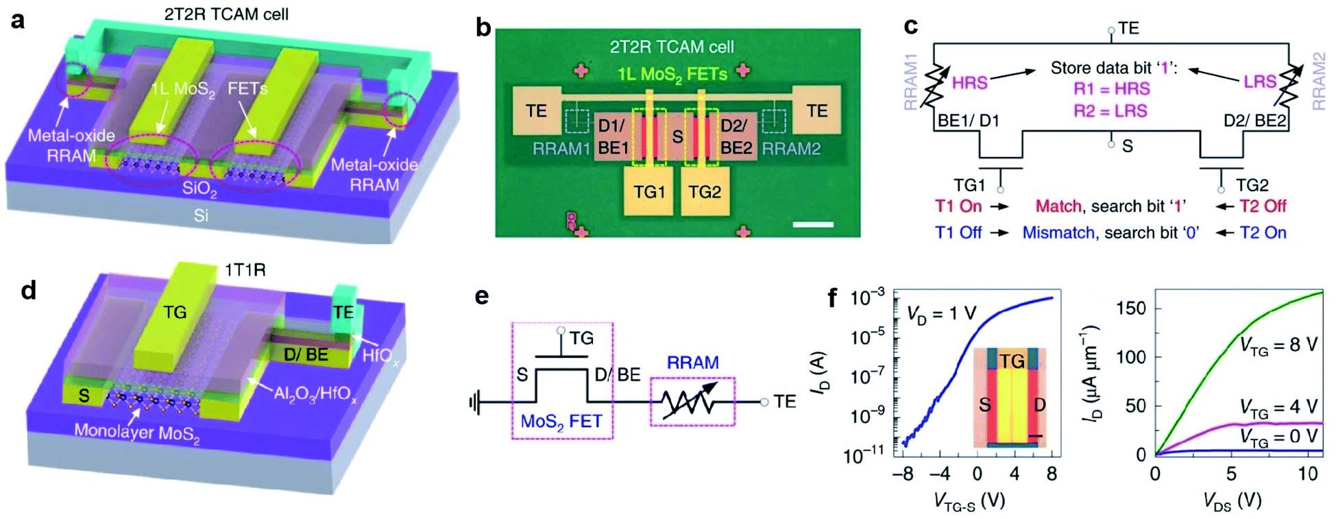 | ||
| Fig. 13 2T2R TMD-TCAM and 1T1R component with MoS2-FET. (a) 3D schematic illustration of the 2T2R TCAM cell, with two MoS2 FETs and two HfOx-based RRAMs. (b) Top-view optical image of the 2T2R TCAM cell 1. Scale bar: 50 μm. (c) Circuit diagram of the 2T2R TCAM cell showing the definition of match and mismatch states, with the stored data bit ‘1’. (d) 3D schematic of the 1T1R structure, as a component of the 2T2R TCAM cell. (e) Circuit diagram of the 1T1R structure. Measured representative Id − VTG-S (f) and Id − Vds (g) characteristics of the top-gated monolayer MoS2-FET with 25 nm HfOx as the gate dielectric, with W = 50 μm, L = 0.8 μm, measured at VBG = 0 V and with the source grounded.112 Reproduced with permission from ref. 112, copyright 2019 Springer Nature. | ||
4.3 Photodetectors
Owing to the atomic thickness, tunable bandgap, and strong light interaction, the practical application of 2D MoS2 is attractive in environment-friendly optoelectronic devices, especially in photodetectors. For instance, Zhang et al.120 demonstrated high gain phototransistors based on CVD-grown monolayer MoS2 with a photoresponsivity up to 2200 A/W under the irradiation of 532 nm laser. Lim et al.121 fabricated MoS2-based visible-light photodetector arrays based on top-gated MoS2-FETs on a 4-inch SiO2/Si wafer with a 1-buty-3-methylimidazolium (BmimPF6) liquid dielectric. As shown in Fig. 14, these 100 devices exhibit a narrow photocurrent distribution (0.05–0.1 nA) at an illumination power of 12.5 mW cm−2 and a voltage bias of 20 V. Under periodic illumination using a halogen lamp with a tunable power, the photocurrent demonstrated abrupt switching behavior, regardless of the bias voltages. The photocurrent is linearly dependent on the voltage and illumination power due to the increase in the carrier drift velocity and the carrier generation rate, suggesting excellent tunability for multifaceted optoelectronic applications. Liu et al.36 developed MoS2/PbS hybrid device arrays based on the CVD-synthesized monolayer MoS2 and PbS quantum dots. The hybrid devices were obtained by spin-coating PbS quantum dots on the MoS2-FET array and exhibited broad spectral photoresponse (457–1064 nm), rapid response rate, and high responsivity of approximately 1.8 × 10⁴ A W−1. Kim et al.120 demonstrated phototransistors based on the monolayer MoS2 film with uniform substitutional doping on the 2-inch wafers. The Nb-doped MoS2 devices exhibited improved optoelectronic performance and stable electrical properties in ambient conditions. The obtained photoresponsivity, detectivity, and response rate were 5 × 10⁵ A W−1, 5 × 10¹² Jones, and 5 m s, respectively, suggesting great feasibility of practical applications based on functionalized 2D MoS2. Kim et al.123 reported fully printed transparent MoS2 phototransistor arrays on flexible polyethylene-naphthalate (PEN) substrates. The patterned CVD-synthesized MoS2 film was transferred onto a PEN substrate, followed by sequentially inkjet-printed poly(3,4-ethylenedioxythiophene) polystyrenesulfonate (PEDOT:PSS) source/drain electrodes, a cross-linked PVP gate dielectric layer, and a PEDOT:PSS top-gate electrode. The printed transparent MoS2 phototransistors exhibited not only comparable photoresponsivity and photodetectivity over the entire visible range from 400 to 800 nm but also good stability under repetitive bending cycle tests. Furthermore, the performance of MoS2 photodetectors can be dramatically improved and optimized by forming MoS2 hybrid heterostructures with graphene, other TMD, etc.124–132 The photoresponsivity, detectivity, and photoresponse of the MoS2-based hybrid photodetectors can vary by several orders of magnitude depending on the nature of the heterostructures, doping situation, wavelengths, and intensity of the applied incident power. The flexible photodetectors developed from MoS2 and MoS2-based hybrid heterostructures provide great potential for the future application in integrated nano-optoelectronic systems and wearable devices.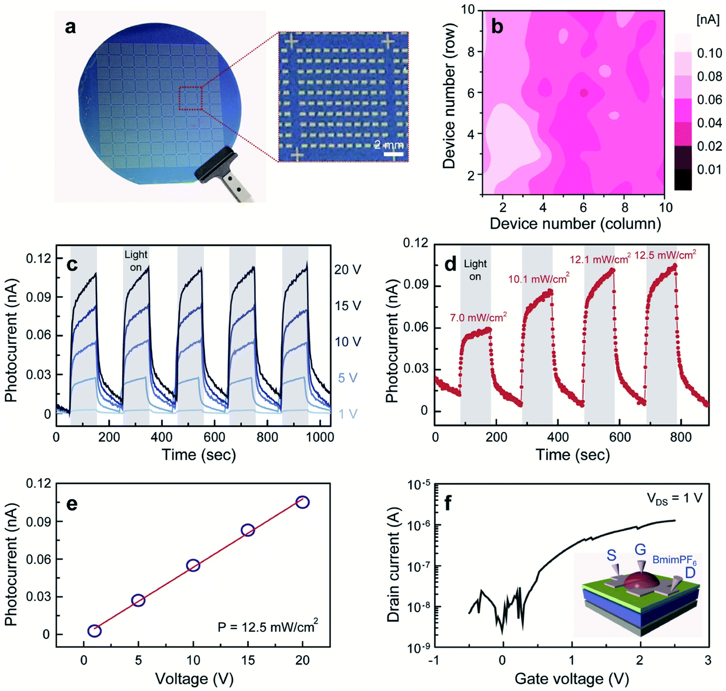 | ||
| Fig. 14 (a) A photograph of homogeneous MoS2-based visible-light photodetector arrays on a 4-inch SiO2/Si wafer. (b) A spatially resolved photocurrent map of the 100 devices recorded at P = 12.5 mW cm−2 and V = 20 V. (c) Representative time-resolved photocurrents of the device recorded at P = 12.5 mW cm−2 for different bias voltages. (d) Time-dependent photocurrents of the device at V = 20 V for different illumination light powers. (e) A plot of device photocurrents as a function of applied voltage. (f) A typical transfer curve of the electrochemically gate-tuned MoS2-FET at Vds = 1 V and (inset) a schematic illustration of MoS2-FET.121 Reproduced with permission from ref. 121, copyright 2016 John Wiley and Sons. | ||
5. Conclusion and outlook
This review focused on the recent advances in the wafer-scale monolayer MoS2 synthesis and 2D MoS2-FET for practical application in electronics and optoelectronics. Wafer-scale monolayer MoS2 have been realized by different methods, including Au-assisted exfoliation, CVD, thin film sulfurization, MOCVD, VLS method, ALD, and the thermolysis of thiosalts. However, these synthetic methods show different advantages and shortcomings in MoS2 productions and related costs. Au-assisted exfoliation is convenient in laboratory research, but the repetition rate and size uniformity are difficult to control. CVD is relatively low-cost and possible to mass produce for wide applications, although the growth rate and repetition rate should be improved. The thin film sulfurization method is low-cost but leaves behind some problems, such as difficulty in controlling the thickness of Mo and the MoOx layer. MOCVD exhibits great advantages in producing high quality MoS2 monolayers with high repetition rate, but the long production cycle and special production conditions lead to the high cost. The VLS method seems low-cost in wafer-scale MoS2 monolayers syntheses, but it is still at the earlier stages of research. ALD can realize wafer-scale MoS2 monolayers with high repetition rate and good uniformity but in complex production processes with high cost. Thermolysis of thiosalts based on the thermal decomposition of thiosalts results in low cost, but the thickness is difficult to control, leading to low repetition rate for MoS2 synthesis. Based on the overall consideration of above synthetic methods, CVD and MOCVD present obvious advantages in the synthesis of wafer-scale MoS2 monolayers with large quantities. Even though there is considerable room for improvement in monolayer MoS2 synthesis, more and more efforts are being made to optimize the growth conditions and reduce the costs. Thus, wafer-scale high-quality MoS2 monolayers could be obtained in the near future with the desired thickness, good uniformity, large grain size, and less defects.The 2D MoS2-FET array with different configurations utilizes high-quality MoS2 as the channel and exhibits favorable performance. The MoS2-FET fabricated from the wafer-scale monolayer MoS2 demonstrates a mobility of several tens and an on/off ratio even up to 1010, demonstrating great potential in practical applications based on basic MoS2-FET for modern integrated electronics and flexible optoelectronics, such as logic circuits, memory devices, and photodetectors. Although significant progress has been made in research laboratories for monolayer MoS2 synthesis and MoS2-FET devices, the mass production of wafer-scale and high-quality 2D MoS2-FET is still challenging. In the future, more new investigations are needed to fulfill the usage demands of fundamental studies and practical applications, especially different circuit-level applications. The repeatability of wafer-scale uniform MoS2 synthesis should be improved for device applications. Functionalization and strain engineering based on wafer-scale monolayer MoS2 are needed to be considered for the improvement of carrier mobility and PL quantum yields. The precise control of MoS2 transfer and MoS2-channel patterning is required for integrated devices fabrication. Further study on the effect of photolithography and the lift-off process on monolayer MoS2 is also necessary for the performance improvement in basic MoS2-FET. Looking forward, with more comprehensive advancement in both fundamental research and practical application, 2D MoS2 film and MoS2-FET will demonstrate great potential and prospect in realizing MoS2-based integrated electronics and flexible optoelectronics for modern applications.
Conflicts of interest
There are no conflicts to declare.Acknowledgements
The work was supported by the National Natural Science Foundation of China (NSFC, 62075131), China Postdoctoral Science Foundation (2020M671168) and the Shanghai Rising-Star Program (18QA1403200).References
- S. Manzeli, D. Ovchinnikov, D. Pasquier, O. V. Yazyev and A. Kis, Nat. Rev. Mater., 2017, 2, 17033 CrossRef CAS.
- J. Zhou, J. Lin, X. Huang, Y. Zhou, Y. Chen, J. Xia, H. Wang, Y. Xie, H. Yu, J. Lei, D. Wu, F. Liu, Q. Fu, Q. Zeng, C. Hsu, C. Yang, L. Lu, T. Yu, Z. Shen, H. Lin, B. I. Yakobson, Q. Liu, K. Suenaga, G. Liu and Z. Liu, Nature, 2018, 556, 355–359 CrossRef CAS PubMed.
- Z. Lin, Y. Huang and X. Duan, Nat. Electron., 2019, 2, 378–388 CrossRef.
- G. R. Bhimanapati, Z. Lin, V. Meunier, Y. Jung, J. Cha, S. Das, D. Xiao, Y. Son, M. S. Strano, V. R. Cooper, L. Liang, S. G. Louie, E. Ringe, W. Zhou, S. S. Kim, R. R. Naik, B. G. Sumpter, H. Terrones, F. Xia, Y. Wang, J. Zhu, D. Akinwande, N. Alem, J. A. Schuller, R. E. Schaak, M. Terrones and J. A. Robinson, ACS Nano, 2015, 9, 11509–11539 CrossRef CAS PubMed.
- K. F. Mak, C. Lee, J. Hone, J. Shan and T. F. Heinz, Phys. Rev. Lett., 2010, 105, 136805 CrossRef PubMed.
- S. Zeng, Z. Tang, C. Liu and P. Zhou, Nano Res., 2020 DOI:10.1007/s12274-020-2945-z.
- L. Yu, E. Damak, D. Radhakrishna, U. Ling, X. Zubair, A. Lin, Y. Zhang, Y. Chuang, M.-H. Lee, Y.-H. Antoniadis, D. Kong, J. Chandrakasan, A. Palacios and T. Design, Nano Lett., 2016, 16, 6349–6356 CrossRef CAS PubMed.
- L. Wang, L. Chen, S. L. Wong, X. Huang, W. Liao, C. Zhu, Y. Lim, D. Li, X. Liu, D. Chi and K. Ang, Adv. Electron. Mater., 2019, 5, 1900393 CrossRef.
- C. Liu, H. Chen, X. Hou, H. Zhang, J. Han, Y.-G. Jiang, X. Zeng, D. W. Zhang and P. Zhou, Nat. Nanotechnol., 2019, 14, 662–667 CrossRef CAS PubMed.
- Z. Lin, Y. Liu, U. Halim, M. Ding, Y. Liu, Y. Wang, C. Jia, P. Chen, X. Duan, C. Wang, F. Song, M. Li, C. Wan, Y. Huang and X. Duan, Nature, 2018, 562, 254–258 CrossRef CAS PubMed.
- H. Wang, C. Li, P. Fang, Z. Zhang and J. Z. Zhang, Chem. Soc. Rev., 2018, 47, 6101–6127 RSC.
- W. Liao, S. Zhao, F. Li, C. Wang, Y. Ge, H. Wang, S. Wang and H. Zhang, Nanoscale Horiz., 2020, 5, 787–807 RSC.
- N. Li, Q. Wang, C. Shen, Z. Wei, H. Yu, J. Zhao, X. Lu, G. Wang, C. He, L. Xie, J. Zhu, L. Du, R. Yang, D. Shi and G. Zhang, Nanoscale Horiz., 2020, 3, 711–717 CAS.
- Y. Wang, J. C. Kim, R. J. Wu, J. Martinez, X. Song, J. Yang, F. Zhao, A. Mkhoyan, H. Y. Jeong and M. Chhowalla, Nature, 2019, 568, 70–74 CrossRef CAS PubMed.
- J. Sun, X. Li, W. Guo, M. Zhao, X. Fan, Y. Dong, C. Xu, J. Deng and Y. Fu, Crystals, 2017, 7, 1–11 Search PubMed.
- H. Li, Y. Li, A. Aljarb, Y. Shi and L. J. Li, Chem. Rev., 2018, 118, 6134–6150 CrossRef CAS PubMed.
- J. Wang, T. Li, Q. Wang, W. Wang, R. Shi, N. Wang, A. Amini and C. Cheng, Mater. Today Adv., 2020, 8, 100098 CrossRef.
- T. Kim, J. Mun, H. Park, D. Joung, M. Diware, C. Won, J. Park, S. Jeong and S. Kang, Nanotechnology, 2017, 28, 18LT01 CrossRef PubMed.
- N. B. Shinde, B. Francis, M. S. R. Rao, B. D. Ryu and S. K. Eswaran, APL Mater., 2019, 7, 081113 CrossRef.
- C. Yoo, M. G. Kaium, L. Hurtado, H. Li, S. Rassay, J. Ma, T. Ko, S. S. Han, M. S. Shawkat, K. H. Oh, H. Chung and Y. Jung, ACS Appl. Mater. Interfaces, 2020, 12, 25200–25210 CrossRef CAS PubMed.
- J. Mun, H. Park, J. Park, D. Joung, S.-K. Lee, J. Leem, J.-M. Myoung, J. Park, S.-H. Jeong, W. Chegal, S. W. Nam and S.-W. Kang, ACS Appl. Electron. Mater., 2019, 1, 608–616 CrossRef CAS.
- Z. Cai, B. Liu, X. Zou and H. M. Cheng, Chem. Rev., 2018, 118, 6091–6133 CrossRef CAS PubMed.
- X. Xu, G. Das, X. He, M. N. Hedhili, E. D. Fabrizio, X. Zhang and H. N. Alshareef, Adv. Funct. Mater., 2019, 29, 1901070 CrossRef.
- P. Yang, X. Zou, Z. Zhang, M. Hong, J. Shi, S. Chen, J. Shu, L. Zhao, S. Jiang, X. Zhou, Y. Huan, C. Xie, P. Gao, Q. Chen, Q. Zhang, Z. Liu and Y. Zhang, Nat. Commun., 2018, 9, 979 CrossRef PubMed.
- J. Shim, S. H. Bae, W. Kong, D. Lee, K. Qiao, D. Nezich, Y. J. Park, R. Zhao, S. Sundaram, X. Li, H. Yeon, C. Choi, H. Kum, R. Yue, G. Zhou, Y. Ou, K. Lee, J. Moodera, X. Zhao, J. H. Ahn, C. Hinkle, A. Ougazzaden and J. Kim, Science, 2018, 362, 665–670 CrossRef CAS PubMed.
- G. Magda, J. Pető, G. Dobrik, C. Hwang, L. P. Biró and L. Tapasztó, Sci. Rep., 2015, 5, 14714 CrossRef CAS PubMed.
- S. B. Desai, S. R. Madhvapathy, M. Amani, D. Kiriya, M. Hettick, M. Tosun, Y. Zhou, M. Dubey, J. W. Ager, D. Chrzan and A. Javey, Adv. Mater., 2016, 28, 4053–4058 CrossRef CAS PubMed.
- M. Velický, G. E. Donnelly, W. R. Hendren, S. McFarland, D. Scullion, W. J. I. DeBenedetti, G. C. Correa, Y. Han, A. J. Wain, M. A. Hines, D. A. Muller, K. S. Novoselov, H. D. Abruña, R. M. Bowman, E. J. G. Santos and F. Huang, ACS Nano, 2018, 12, 10463–10472 CrossRef PubMed.
- F. Liu, W. Wu, Y. Bai, S. H. Chae, Q. Li, J. Wang, J. Hone and X. Y. Zhu, Science, 2020, 367, 903–906 CrossRef CAS PubMed.
- Y. Huang, Y. Pan, R. Yang, L. Bao, L. Meng, H. Luo, Y. Cai, G. Liu, W. Zhao, Z. Zhou, L. Wu, Z. Zhu, M. Huang, L. Liu, L. Liu, P. Cheng, K. Wu, S. Tian, C. Gu, Y. Shi, Y. Guo, Z. Cheng, J. Hu, L. Zhao, E. Sutter, P. Sutter, Y. Wang, W. Ji, X. Zhou, H. Gao, X. Zhou and H. Gao, Nat. Commun., 2020, 11, 2453 CrossRef CAS PubMed.
- H. Yu, M. Liao, W. Zhao, G. Liu, X. J. Zhou, Z. Wei, X. Xu, K. Liu, Z. Hu, K. Deng, S. Zhou, J. Shi, L. Gu, C. Shen, T. Zhang, L. Du, L. Xie, J. Zhu, W. Chen, R. Yang, D. Shi and G. Zhang, ACS Nano, 2017, 11, 12001–12007 CrossRef CAS PubMed.
- H. Xu, H. Zhang, Z. Guo, Y. Shan, S. Wu, J. Wang, W. Hu, H. Liu, Z. Sun, C. Luo, X. Wu, Z. Xu, D. Zhang, W. Bao and P. Zhou, Small, 2018, 14, 1803465 CrossRef PubMed.
- Q. Wang, N. Li, J. Tang, J. Zhu, Q. Zhang, Q. Jia, Y. Lu, Z. Wei, H. Yu, Y. Zhao, Y. Guo, L. Gu, G. Sun, W. Yang, R. Yang, D. Shi and G. Zhang, Nano Lett., 2020, 20, 7193–7719 CrossRef CAS PubMed.
- T. He, Y. Li, Z. Zhou, C. Zeng, L. Qiao, C. Lan, Y. Yin, C. Li and Y. Liu, 2D Mater., 2019, 6, 025030 CrossRef CAS.
- S. Durairaj, P. Krishnamoorthy, N. Raveendran, B. Ryu, C. Hong, T. H. Seoc and S. Chandramohan, Nanoscale Adv., 2020, 2, 4106–4116 RSC.
- L. Liu, K. Ye, Z. Yu, Z. Jia, J. Xiang, A. Nie, F. Wen, C. Mu, B. Wang, Y. Li, Y. Gong and Z. Liu, 2D Mater., 2020, 7, 025020 CrossRef CAS.
- P. Yang, S. Zhang, S. Pan, B. Tang, Y. Liang, X. Zhao, Z. Zhang, J. Shi, Y. Huan, Y. Shi, S. J. Pennycook, Z. Ren, G. Zhang, Q. Chen, X. Zou, Z. Liu and Y. Zhang, ACS Nano, 2020, 14, 5036–5045 CrossRef CAS PubMed.
- S. Tong, H. Medina, W. Liao, J. Wu, W. Wu, J. Chai, M. Yang, A. Abutaha, S. Wang, C. Zhu, K. Hippalgaonkar and D. Chi, ACS Appl. Mater. Interfaces, 2019, 11, 14239–14248 CrossRef CAS PubMed.
- P. Sun, Y. Liu, J. Ma, W. Li, K. Zhang and Y. Yuan, CrystEngComm, 2019, 21, 6969–6977 RSC.
- Y. Lim, K. Priyadarshi, F. Bussolotti, P. K. Gogoi, X. Cui, M. Yang, J. Pan, S. W. Tong, S. Wang, S. J. Pennycook, K. E. J. Goh, A. T. S. Wee, S. L. Wong and D. Chi, ACS Nano, 2018, 12, 1339–1349 CrossRef CAS PubMed.
- G. Li, X. Wang, B. Han, W. Zhang, S. Qi, Y. Zhang, J. Qiu, P. Gao, S. Guo, R. Long, L. Tan, X. Song and N. Liu, J. Phys. Chem. Lett., 2020, 11, 1570–1577 CrossRef CAS PubMed.
- F. Liao, J. Yu, Z. Gu, Z. Yang, T. Hasan, S. Linghu, J. Peng, W. Fang, S. Zhuang, M. Gu and F. Gu, Sci. Adv., 2019, 5, eaax7398 CrossRef CAS PubMed.
- F. Gu, L. Zhang, Y. Zhu and H. Zeng, Laser Photonics Rev., 2015, 9, 682 CrossRef CAS.
- F. Gu, F. Xie, X. Lin, S. LingHu, W. Fang, H. Zeng, L. Tong and S. Zhuang, Light: Sci. Appl., 2017, 6, e17061 CrossRef CAS PubMed.
- J. H. Kim, T. Ko, E. Okogbue, S. S. Han, M. S. Shawkat, M. G. Kaium, K. H. Oh, H. Chung and Y. Jung, Sci. Rep., 2019, 9, 1641 CrossRef PubMed.
- S. Jo, Y. Li, A. Singh, A. Kumar, S. Frisone, J. M. LeBeau and R. Jaramillo, J. Vac. Sci. Technol., A, 2020, 38, 013405 CrossRef CAS.
- H. Park, N. Liu, B. H. Kim, S. H. Kwon, S. Baek, S. Kim, H. Lee, Y. J. Yoon and S. Kim, ACS Appl. Mater. Interfaces, 2020, 12, 20645–20652 CrossRef CAS PubMed.
- K. Almeida, M. Wurch, A. Geremew, K. Yamaguchi, T. A. Empante, M. D. Valentin, M. Gomez, A. J. Berges, G. Stecklein, S. Rumyantsev, J. Martinez, A. A. Balandin and L. Bartels, ACS Appl. Mater. Interfaces, 2018, 10, 33457–33463 CrossRef CAS PubMed.
- H. Choi, Y. Jung, S. Lee, S. Kang, D. Seo, H. Kim, H. Choi, G. Lee and Y. Cho, Cryst. Growth Des., 2020, 20, 2698–2705 CrossRef CAS.
- X. Xu, Z. Wang, S. Lopatin, M. A. Quevedo-Lopez and H. N. Alshareef, 2D Mater., 2019, 6, 015030 CrossRef CAS.
- X. Xu, C. Zhang, M. K. Hota, Z. Liu, X. Zhang and H. N. Alshareef, Adv. Funct. Mater., 2020, 30, 1908040 CrossRef CAS.
- M. Shi, L. Chen, T. Zhang, J. Xu, H. Zhu, Q. Sun and D. Zhang, Small, 2017, 13, 16031571 Search PubMed.
- B. Kalanyan, W. A. Kimes, R. Beams, S. J. Stranick, E. Garratt, I. Kalish, A. V. Davydov, R. K. Kanjolia and J. E. Maslar, Chem. Mater., 2017, 29, 6279–6288 CrossRef CAS PubMed.
- M. B. Shinde, B. Francis, M. S. R. Rao, B. D. Ryu, S. Chandramohan and S. K. Eswara, APL Mater., 2019, 7, 081113 CrossRef.
- N. B. Shinde, B. D. Ryu, K. Meganathan, B. Francis, C. Hong, S. Chandramohan and S. K. Eswaran, ACS Appl. Nano Mater., 2020, 3, 7371–7376 CrossRef CAS.
- H. Cun, M. Macha, H. Kim, K. Liu, Y. Zhao, T. L. Grange, A. Kis and A. Radenovic, Nano Res., 2019, 12, 2646–2652 CrossRef CAS.
- M. Seol, Mi. Lee, H. Kim, K. W. Shin, Y. Cho, I. Jeon, M. Jeong, H. Lee, J. Park and H. Shin, Adv. Mater., 2020, 32, e2003542 CrossRef PubMed.
- S. Li, Y.-C. Lin, W. Zhao, J. Wu, Z. Wang, Z. Hu, Y. Shen, D.-M. Tang, J. Wang and Q. Zhang, Nat. Mater., 2018, 17, 535–542 CrossRef CAS PubMed.
- S. Li, Y. Lin, T. Taniguchi and M. Osada, Nanoscale, 2019, 11, 16122–16129 RSC.
- M. Chang, P. Ho, M. Tseng, F. Lin, C. Hou, I. Lin, H. Wang, P. Huang, C. Chiang, Y. Yang, I. Wang, H. Du, C. Wen, J. Shyue, C. Chen, K. Chen, P. Chiu and L. Chen, Nat. Commun., 2020, 11, 3682 CrossRef CAS PubMed.
- Y. Kim, J.-G. Song, Y. J. Park, G. H. Ryu, S. J. Lee, J. S. Kim, P. J. Jeon, C. W. Lee, W. J. Woo, T. Choi, H. Jung, H. Lee, J.-M. Myoung, S. Im, Z. Lee, J.-H. Ahn, J. Park and H. Kima, Sci. Rep., 2016, 6, 18754 CrossRef CAS PubMed.
- Y. Huang, L. Liu, W. Zhao and Y. Chen, Thin Solid Films, 2017, 624, 101–105 CrossRef CAS.
- A. U. Mane, S. Letourneau, D. J. Mandia, J. Liu, J. A. Libera, Y. Lei, Q. Peng, E. Graugnard and J. W. Elam, J. Vac. Sci. Technol., A, 2018, 36, 01A125 CrossRef.
- J. Cai, X. Han, X. Wang and X. Meng, Matter, 2020, 2, 587–630 CrossRef.
- Y. Jang, S. Yeoc, H.-B.-R. Lee, H. Kim and S.-H. Kim, Appl. Surf. Sci., 2016, 365, 160–165 CrossRef CAS.
- J. Pyeon, S. H. Kim, D. S. Jeong, S.-H. Baek, C.-Y. Kang, J.-S. Kima and Se. K. Kim, Nanoscale, 2016, 8, 10792–10798 RSC.
- T. Jurca, M. J. Moody, A. Henning, J. D. Emery, B. Wang, J. M. Tan, T. L. Lohr, L. J. Lauhon and T. J. Marks, Angew. Chem., Int. Ed., 2017, 56, 4991–4995 CrossRef CAS PubMed.
- H. Liu, L. Chen, H. Zhu, Q. Sun, S. Ding, P. Zhou and D. W. Zhang, Nano Res., 2020, 13, 1644–1650 CrossRef CAS.
- R. Ionescu, B. Campbell, R. Wu, E. Aytan, A. Patalano, I. Ruiz, S. W. Howell, A. E. McDonald, T. E. Beechem, K. A. Mkhoyan, M. Ozkan and C. S. Ozkan, Sci. Rep., 2017, 7, 6419 CrossRef PubMed.
- S. M. Islam, J. D. Cain, F. Shi, Y. He, L. Peng, A. Banerjee, K. S. Subrahmanyam, Y. Li, S. Ma, V. P. Dravid, M. Grayson and M. G. Kanatzidis, Chem. Mater., 2018, 30, 3847–3853 CrossRef CAS.
- Y. R. Lim, J. K. Han, S. K. Kim, Y. B. Lee, Y. Yoon, S. J. Kim, B. K. Min, Y. Kim, C. Jeon, S. Won, J. -H. Kim, W. Song, S. Myung, S. S. Lee, K. -S. An and J. Lim, Adv. Mater., 2018, 30, 1705270 CrossRef PubMed.
- S. Park, A. Lee, K. Choi, S. Hyeong, S. Bae, J. Hong, T. Kim, B. H. Hong and S. Lee, ACS Nano, 2020, 14, 8485–8494 CrossRef CAS PubMed.
- X. Jing, Y. Illarionov, E. Yalon, P. Zhou, T. Grasser, Y. Shi and M. Lanza, Adv. Funct. Mater., 2020, 30, 1901971 CrossRef CAS.
- N. D. Bharathi and K. Sivasankaran, J. Semicond., 2018, 39, 104002 CrossRef.
- Y. Kim, A. Kim, G. Zhao, S. Choi, S. Kang, S. Lim, K. Lee, J. Park, B. Lee, M. Hahm, D. Kim, J. Yun, K. Lee and B. Cho, ACS Appl. Mater. Interfaces, 2017, 9, 37146–37153 CrossRef CAS PubMed.
- H. Zhang, X. Guo, W. Niu, H. Xu, Q. Wu, F. Liao, J. Chen, H. Tang, H. Liu, Z. N. Xu, Z. Sun, Z. Qiu, Y. Pu and W. Bao, 2D Mater., 2020, 7, 025019 CrossRef CAS.
- X. Liu, K. Huang, M. Zhao, F. Li and H. Liu, Nanotechnology, 2020, 31, 055707 CrossRef CAS PubMed.
- X. Liu, Y. Chai and Z. Liu, Nanotechnology, 2017, 28, 164004 CrossRef PubMed.
- L. Liu, X. Wang, L. Han, B. Tian, Y. Chen, G. Wu, D. Li, M. Yan, T. Wang, S. Sun, H. Shen, T. Lin, J. Sun, C. Duan, J. Wang, X. Meng and J. Chu, AIP Adv., 2017, 7, 065121 CrossRef.
- Y. Zhu, Y. Li, G. Arefe, R. A. Burke, C. Tan, Y. Hao, X. Liu, X. Liu, W. Yoo, M. Dubey, Q. Lin and J. C. Hone, Nano Lett., 2018, 18, 3807–3813 CrossRef CAS.
- Y. Illarionov, Ar G. Banshchikov, D. K. Polyushkin, S. Wachter, T. Knobloch, M. Thesberg, M. Vexler, M. Waltl, M. Lanza, N. S. Sokolov, T. Mueller and T. Grasser, 2D Mater., 2019, 6, 045004 CrossRef CAS.
- I. Lee, J. N. Kim, W. T. Kang, Y. S. Shin, B. H. Lee and W. J. Yu, ACS Appl. Mater. Interfaces, 2020, 12, 2854–2861 CrossRef CAS PubMed.
- X. Zou, L. Liu, J. G. Xu, H. Wang and W. Tang, ACS Appl. Mater. Interfaces, 2020, 12, 32943–32950 CrossRef CAS PubMed.
- M. A. Rodder, S. Vasishta and A. Dodabalapur, ACS Appl. Mater. Interfaces, 2020, 12, 33926–33933 CrossRef CAS PubMed.
- X. Cui, E. -M. Shih, L. A. Jauregui, S. H. Chae, Y. D. Kim, B. Li, D. Seo, K. Pistunova, J. Yin, J. -H. Park, H. -J. Choi, Y. H. Lee, K. Watanabe, T. Taniguchi, P. Kim, C. R. Dean and J. C. Hone, Nano Lett., 2017, 17, 4781 CrossRef CAS PubMed.
- J. Jiang, Y. Zhang, A. Wang, J. Duan, H. Ji, J. Pang, Y. Sang, X. Feng, H. Liu and L. Han, ACS Appl. Electron. Mater., 2020, 2, 2132–2140 CrossRef CAS.
- J. Wei, S. Yu, X. Shan, K. Lan, X. Yang, K. Zhang and G. Qin, ACS Appl. Mater. Interfaces, 2020, 12, 38306–38313 CrossRef CAS PubMed.
- Y. Lan, P. Chen, Y. Lin, M. Li, L. Li, Y. Tu, F. Yang, M. Chen and K. Li, Nanoscale Horiz., 2019, 4, 683–688 RSC.
- D. H. Zhao, Z. L. Tian, H. Liu, Z. H. Gu, H. Zhu, L. Chen, Q. Q. Sun and D. W. Zhang, ACS Appl. Mater. Interfaces, 2020, 12, 14308–14314 CrossRef CAS PubMed.
- Z. Hu, Z. Wu, C. Han, J. He, Z. Ni and W. Chen, Chem. Soc. Rev., 2018, 47, 3100–3128 RSC.
- D. S. Schulman, A. J. Arnold and S. Das, Chem. Soc. Rev., 2018, 47, 3037–3058 RSC.
- K. Andrews, A. Bowman, U. Rijal, P. Chen and Z. Zhou, ACS Nano, 2020, 14, 6232–6241 CrossRef CAS PubMed.
- X. Cui, E. Shih, L. A. Jauregui, S. Chae, Y. Kim, B. Li, D. Seo, K. Pistunova, J. Yin, J. Park, H. Choi, Y. Lee, K. Watanabe, T. Taniguchi, P. Kim, C. R. Dean and J. C. Hone, Nano Lett., 2017, 17, 4781–47864 CrossRef CAS PubMed.
- S. Chen, S. Kim, W. Chen, J. Yuan, R. Bashir, J. Lou, A. M. Zande and W. P. King, Nano Lett., 2019, 19, 2092–2098 CrossRef CAS PubMed.
- M. S. M. Saifullah, M. Asbahi, M. B.-K. Kiyani, S. S. Liow, S. B. Dolmanan, A. M. Yong, E. A. H. Ong, A. I. Saifullah, H. R. Tan, N. Dwivedi, T. Dutta, R. Ganesan, S. Valiyaveettil, K. S. L. Chon and S. Tripathy, ACS Appl. Mater. Interfaces, 2020, 12, 116772–116781 CrossRef PubMed.
- S. Chee and M. Ham, Adv. Mater. Interfaces, 2020, 7, 2000762 CrossRef CAS.
- Y. Wang, X. Bai, J. Chu, H. Wang, G. Rao, X. Pan, X. Du, K. Hu, X. Wang, C. Gong, C. Yin, C. Yang, C. Yan, C. Wu, Y. Shuai, X. Wang, M. Liao and J. Xiong, Adv. Mater., 2020, 32, 2005353 CrossRef CAS PubMed.
- G. H. Shin, G. Lee, E. An, C. Park, H. J. Jin, K. J. Lee, D. S. Oh, J. S. Kim, Y. Choi and S. Choi, ACS Appl. Mater. Interfaces, 2020, 12, 5106–5112 CrossRef CAS PubMed.
- S. Zhang, H. Xu, F. Liao, Y. Sun, K. Ba, Z. Sun, Z. Qiu, Z. Xu, H. Zhu, L. Chen, Q. Sun, P. Zhou, W. Bao and D. W. Zhang, Nanotechnology, 2019, 30, 174002 CrossRef CAS PubMed.
- F. Liao, Z. Guo, Y. Wang, Y. Xie, S. Zhang, Y. Sheng, H. Tang, Z. Xu, A. Riaud, P. Zhou, J. Wan, M. S. Fuhrer, X. Jiang, D. W. Zhang, Y. Chai, Y. Chai and W. Bao, ACS Appl. Electron. Mater., 2020, 2, 111–119 CrossRef CAS.
- L. Bao, J. Zhu, Z. Yu, R. Jia, Q. Cai, Z. Wang, L. Xu, Y. Wu, Y. Yang, Y. Cai and R. Huang, ACS Appl. Mater. Interfaces, 2019, 11, 41482–41489 CrossRef CAS PubMed.
- S. Yang, S. Jang, D. Choi, S. D. Namgung, H.-J. Kim and J.-Y. Kwon, Phys. Status Solidi RRL, 2019, 13, 1900142 CrossRef.
- J. Du, C. Ge, H. Riahi, E. Guo, M. He, C. Wang, G. Yang and K. Jin, Adv. Electron. Mater., 2020, 6, 1901408 CrossRef CAS.
- Z. Liu, P. Wang, Y. Wang, Y. Huang and X. Duan, Nano Res., 2020, 13, 1943–1947 CrossRef.
- P. Prasad, M. Garga and U. Chandni, Nanoscale, 2020, 12, 23817–23823 RSC.
- S. S. Chee, J. H. Lee, K. Lee and M. H. Ham, ACS Appl. Mater. Interfaces, 2020, 12, 4129–4134 CrossRef CAS PubMed.
- L. Xie, M. Liao, S. Wang, H. Yu, L. Du, J. Tang, J. Zhao, J. Zhang, P. Chen, X. Lu, G. Wang, G. Xie, R. Yang, D. Shi and G. Zhang, Adv. Mater., 2017, 29, 1702522 CrossRef PubMed.
- Y. Liu, J. Guo, E. Zhu, L. Liao, S.-J. Lee, M. Ding, I. Shakir, V. Gambin, Y. Huang and X. Duan, Nature, 2018, 557, 696–700 CrossRef CAS PubMed.
- T. B. Zhang, H. Liu, Y. Wang, H. Zhu, L. Chen, Q. Sun and D. W. Zhang, Phys. Status Solidi RRL, 2019, 13, 1900018 CrossRef.
- S. S. Chee, H. Jang, K. Lee and M.-H. Ham, ACS Appl. Mater. Interfaces, 2020, 12, 31804–31809 CrossRef CAS PubMed.
- S. Wachter, D. K. Polyushkin, O. Bethge and T. Mueller, Nat. Commun., 2017, 8, 14948 CrossRef CAS.
- R. Yang, H. Li, K. K. Smithe, T. R. Kim, K. Okabe, E. Pop, J. A. Fan and H.-S. P. Wong, Nat. Electron., 2019, 2, 108–114 CrossRef.
- R. Yang, H. Li, K. K. H. Smithe, T. R. Kim, K. Okabe, E. Pop, J. A. Fan and H.-S. P. Wong, IEEE Int. Electron Devices Meeting (IEDM), 2017, DOI:10.1109/IEDM.2017.8268423.
- Z. H. Zhang, Z. W. Wang, T. Shi, C. Bi, F. Rao, Y. M. Cai, Q. Liu, H. Q. Wu and P. Zhou, InfoMat, 2020, 2, 261–290 CrossRef CAS.
- S. C. Yang, J. Choi, B. C. Jang, W. Hong, G. W. Shim, S. Y. Yang, S. G. Im and S. -Y. Choi, Adv. Electron. Mater., 2019, 5, 1800688 CrossRef.
- J. Tang, Z. Wei, Q. Wang, Y. Wang, B. Han, X. Li, B. Huang, M. Liao, J. Liu, N. Li, Y. Zhao, C. Shen, Y. Guo, X. Bai, P. Gao, W. Yang, L. Chen, K. Wu, R. Yan, D. Shi and G. Zhang, Small, 2020, 16, e2004276 CrossRef.
- X. Wang, H. Tian, H. Zhao, T. Zhang, W. Mao, Y. Qiao, Y. Pang, Y. Li, Y. Yang and T. Ren, Small, 2018, 14, 1702525 CrossRef.
- S. Conti, L. Pimpolari, G. Calabrese, R. Worsley, S. Majee, D. K. Polyushkin, M. Paur, S. Pace, D. H. Keum, F. Fabbri, G. Iannaccone, M. Macucci, C. Coletti, T. Mueller, C. Casiraghi and G. Fiori, Nat. Commun., 2020, 11, 3566 CrossRef CAS PubMed.
- H. S. Nalwa, RSC Adv., 2020, 10, 30529–30602 RSC.
- W. Zhang, J. K. Huang, C. H. Chen, Y. H. Chang, Y. J. Cheng and L. J. Li, Adv. Mater., 2013, 25, 3456–3461 CrossRef CAS.
- Y. R. Lim, W. Song, J. K. Han, Y. B. Lee, S. J. Kim, S. Myung, S. S. Lee, K. S. An, C. J. Choi and J. Lim, Adv. Mater., 2016, 28, 5025–5030 CrossRef CAS PubMed.
- Y. Kim, Y. Kim, H. Bark, B. Kang and C. Lee, ACS Appl. Mater. Interfaces, 2019, 11, 12613–12621 CrossRef CAS PubMed.
- T. Y. Kim, J. Ha, K. Cho, J. Pak, J. Seo, J. Park, J.-K. Kim, S. Chung, Y. Hong and T. Lee, ACS Nano, 2017, 11, 10273–10280 CrossRef CAS PubMed.
- Y. Yang, N. Huo and J. Li, J. Mater. Chem. C, 2017, 5, 11614–11619 RSC.
- F. Li, T. Shen, L. Xu, C. Hu and J. Qi, Adv. Electron. Mater., 2019, 5, 1900803 CrossRef CAS.
- T. Dong, J. Simões and Z. Yang, Adv. Mater. Interfaces, 2020, 7, 1901657 CrossRef CAS.
- Z. He, J. Guo, S. Li, Z. Lei, L. Lin, Y. Ke, W. Jie, T. Gong, Y. Lin, T. Cheng, W. Huang and X. Zhang, Adv. Mater. Interfaces, 2020, 7, 2070050 CrossRef.
- C. Gao, Y. Han, K. Zhang, T. Wei, Z. Jiang, Y. Wei, L. Yin, F. Piccinelli, C. Yao, X. Xie, M. Bettinelli and L. Huang, Adv. Sci., 2020, 7, 2002444 CrossRef CAS PubMed.
- K. Ye, L. Liu, J. Huang, A. Nie, K. Zhai, B. Wang, F. Wen, C. Mu, Z. Zhao, Y. Gong, J. Xiang, Y. Tian and Z. Liu, Adv. Electron. Mater., 2020, 8, 202000168 Search PubMed.
- Y. Cheng, H. Li, B. Liu, L. Jiang, M. Liu, H. Huang, J. Yang, J. He and J. Jiang, Small, 2020, 16, 202070244 Search PubMed.
- H. Wang, C. Li, P. Fang, Z. Zhang and J. Z. Zhang, Chem. Soc. Rev., 2018, 47, 6101–6127 RSC.
- S. Shi, Z. Sun and Y. H. Hu, J. Mater. Chem. A, 2018, 6, 23932–23977 RSC.
- Q. Zhao, Z. Xie, Y. P. Peng, K. Wang, H. Wang, X. Li, H. Wang, J. Chen, H. Zhang and X. Yan, Mater. Horiz., 2020, 7, 1495–1518 RSC.
- P. Das, J. Nash, M. Webb, R. Burns, V. N. Mapara, G. Ghimire, D. Rosenmann, R. Divan, D. Karaiskaj, S. A. McGill, A. V. Sumant, Q. Dai, P. C. Ray, B. Tawade, D. Raghavan, A. Karim and N. R. Pradhan, Nanoscale, 2020, 12, 22904–22916 RSC.
- C. Lan, Z. Shi, R. Cao, C. Li and H. Zhang, Nanoscale, 2020, 12, 11784–11807 RSC.
- G. Wu, X. Wang, Y. Chen, Z. Wang, H. Shen, T. Lin, W. Hu, J. Wang, S. Zhang, X. Meng and J. Chu, Nanotechnology, 2018, 29, 485204 CrossRef PubMed.
- K. Zhang, M. Peng, A. Yu, Y. Fan, J. Zhai and Z. L. Wang, Mater. Horiz., 2019, 6, 826–833 RSC.
- H. Ying, X. Li, H. Wang, Y. Wang, X. Hu, J. Zhang, X. Zhang, Y. Shi, M. Xu and Q. Zhang, Adv. Opt. Mater., 2020, 8, 2000430 CrossRef CAS.
- S. S. Chee, W. J. Lee, Y. R. Jo, M. K. Cho, D. W. Chun, H. Baik, B. -J. Kim, M. -H. Yoon, K. Lee and M. -H. Ham, Adv. Funct. Mater., 2020, 30, 1908147 CrossRef CAS.
- H. Tang, H. Zhang, X. Chen, Y. Wang, X. Zhang, P. Cai and W. Bao, Sci. China Inf. Sci., 2019, 62, 220401 CrossRef.
- D. Wang, Y. Zhou, H. Zhang, R. Zhang, H. Dong, R. Xu, Z. Cheng, Y. He and Z. Wang, Inorg. Chem., 2020, 59, 17356–17363 CrossRef CAS PubMed.
- E. Singh, P. Singh, K. S. Kim, G. Y. Yeom and H. S. Nalwa, ACS Appl. Mater. Interfaces, 2019, 11, 11061–11105 CrossRef CAS PubMed.
| This journal is © The Royal Society of Chemistry 2021 |