
 Open Access Article
 This Open Access Article is licensed under a
 Creative Commons Attribution 3.0 Unported Licence
Giant photoluminescence enhancement in MoSe2 monolayers treated with oleic acid ligands†
Arelo O. A.
Tanoh
 ab,
Jack
Alexander-Webber
c,
Ye
Fan
c,
Nicholas
Gauriot
a,
James
Xiao
a,
Raj
Pandya
a,
Zhaojun
Li
a,
Stephan
Hofmann
c and
Akshay
Rao
*a
ab,
Jack
Alexander-Webber
c,
Ye
Fan
c,
Nicholas
Gauriot
a,
James
Xiao
a,
Raj
Pandya
a,
Zhaojun
Li
a,
Stephan
Hofmann
c and
Akshay
Rao
*a
aCavendish Laboratory, Cambridge, JJ Thomson Avenue, CB3 0HE, Cambridge, UK. E-mail: ar525@cam.ac.uk
bCambridge Graphene Centre, University of Cambridge, 9 JJ Thomson Avenue, CB3 0FA, Cambridge, UK
cDepartment of Engineering, University of Cambridge, JJ Thomson Avenue, CB3 0FA Cambridge, UK
First published on 12th June 2021
Abstract
The inherently low photoluminescence (PL) yields in the as prepared transition metal dichalcogenide (TMD) monolayers are broadly accepted to be the result of atomic vacancies (i.e., defects) and uncontrolled doping, which give rise to non-radiative exciton decay pathways. To date, a number of chemical passivation schemes have been successfully developed to improve PL in sulphur based TMDs i.e., molybdenum disulphide (MoS2) and tungsten disulphide (WS2) monolayers. Studies on solution based chemical passivation schemes for improving PL yields in selenium (Se) based TMDs are however lacking in comparison. Here, we demonstrate that treatment with oleic acid (OA) provides a simple wet chemical passivation method for monolayer MoSe2, enhancing PL yields by an average of 58-fold, while also improving spectral uniformity across the material and reducing the emission linewidth. Excitation intensity dependent PL reveals trap-free PL dynamics dominated by neutral exciton recombination. Time-resolved PL (TRPL) studies reveal significantly increased PL lifetimes, with pump intensity dependent TRPL measurements also confirming trap free PL dynamics in OA treated MoSe2. Field effect transistors show reduced charge trap density and improved on–off ratios after treatment with OA. These results indicate defect passivation by OA, which we hypothesise as ligands passivating chalcogen defects through oleate coordination to Mo dangling bonds. Importantly, this work combined with our previous study on OA treated WS2, verifies OA treatment as a simple solution-based chemical passivation protocol for improving PL yields and electronic characteristics in both selenide and sulphide TMDs – a property that has not been reported previously for other solution-based passivation schemes.
Two-dimensional (2D) (or monolayer) transition metal dichalcogenides (TMDs) continue to attract wide-spread research interest due to their intriguing optical and electronic properties.2–4 A few to hundreds of micron sized monolayers can be isolated from their layered bulk counterparts by overcoming the interlayer van der Waals interaction via various layer by layer exfoliation methods. These include dry mechanical cleavage,4,5 metal assisted exfoliation6 and liquid phase exfoliation (LPE).7 There are also continuous efforts to grow wafer-scale crystalline monolayers via epitaxial growth methods such as chemical vapour deposition (CVD).8 A number of TMDs transition from an indirect optical gap in the bulk crystal to a direct optical gap as a monolayer.9 The direct optical gap, high absorption10 and potentially high charge carrier mobilities of a number of monolayer TMDs have spurred research into their application in optoelectronic devices namely photodetectors, light emitting diodes (LEDs),11 field effect transistors (FETs)3 and on-chip single photon quantum emitters.12 Moreover, the massively reduced dielectric screening gives rise to tightly bound excitons2,9 even at room temperature, thus providing a convenient means to study the many-body exciton–exciton and exciton–charge interactions that give rise to a multitude of exotic neutral excitons13 and charged excitons.14,15
Although monolayer TMDs hold great promise for future optoelectronic applications, the as-prepared monolayers tend to exhibit low photoluminescence quantum efficiency (PLQE).4,11 The persistence of non-radiative pathways in pristine monolayers has been mainly attributed to chalcogen (i.e., S and Se) vacancies,16,17 atomic substitutions18,19 and trion formation.16,20 Chalcogen vacancies (CVs) and atomic substitutions are examples of structural defects which come under the category of point defects.21 CVs in particular are predicted to be the prevalent form of structural defect in newly fabricated monolayers due to their low formation energy.21–23 CVs are known to act as charge traps, where excitons quench non-radiatively due to charge separation, or bind with trapped charges to form trions, which have low radiative efficiency, resulting in an overall reduction in PLQE.16,20 CVs also trap mobile charge carriers, hampering electronic performance. Other structural defects include grain boundaries, which induce local strain, altering the local electronic structure in polycrystalline large area CVD prepared monolayers. In the absence of grain boundaries, as in the single crystal monolayers studied in this work, chalcogen defects are considered to be the dominant structural defect on account of their low formation energy.21–23 Externally induced sources of disorder also undermine the material performance of monolayer TMDs. External sources of disorder originate from the underlying substrate and ambient adsorbates. Substrate induced disorder includes surface strain and unintentional doping. These external perturbations cause charge scattering, charge trapping and local band structure modifications, which hamper electron mobilities and quench monolayer PL, respectively.21 Charged impurities and substrate doping introduce free charge carriers, which can contribute to the conversion of bright neutral excitons to trions.16,20
Methods to improve material performance broadly take two routes: encapsulation or chemical passivation. Encapsulation utilizes the atomically flat dielectric properties of hexagonal boron nitride (hBN), using it as an encapsulation medium24,25 or sub-layer26 that isolates TMD monolayers from doping and disorder imposed by common substrate materials.21 This preserves their intrinsic properties and improves the overall optical quality as indicated by spatially homogeneous narrow linewidths in the PL spectra. Encapsulation with hBN has been shown to suppress exciton–exciton annihilation in monolayer tungsten disulphide (WS2), improving PL, however, at high excitation intensities.27 Large PL enhancement at low excitation density has not been demonstrated with hBN encapsulation alone.
On the other hand, recently, a number of successful chemical passivation schemes have been devised to enhance the PLQE of sulphur based TMDs, namely molybdenum disulphide (MoS2) and tungsten disulphide (WS2). Such methods involve the use of p-doping agents such as 2,3,5,6-tetrafluoro-7,7,8,8-tetracyanoquinodimethane (F4TCNQ),28,29 hydrogen peroxide,30 and sulphuric acid,31 or deposition of a monolayer titanyl phthalocyanine (TiOPc) charge transfer interface.32 These techniques aim to withdraw electrons to suppress the formation of low PLQE trions, promoting dominant neutral exciton recombination. One of the most successful of these chemical treatments has been the use of the non-oxidizing ‘super acid’ bis(trifluoromethane)sulfonimide (TFSI)16,33,34 to treat MoS2 and WS2, leading to large increases in PL. It has been suggested that TFSI acts as a strong electron withdrawing (p-doping) species via comparative studies with gated n-type MoS2 and WS2 monolayers, whereby applying a negative bias suppresses non-radiative pathways via trion formation, leaving dominant neutral exciton recombination and similar PL dynamics to TFSI treated monolayers.20 However, PL dynamics in TFSI treated MoS2 and WS2 have been shown to be trap-limited,1,35 and it has been recently shown that this is due to the presence of sulphur vacancies which remain unpassivated even with the TFSI treatment.36
Recently, the authors of this study demonstrated a 26 and 20 fold increase in WS2 PL and electron mobilities, respectively, via surface treatment with Oleic Acid (OA) ligands, outperforming treatment with TFSI.1 The OA treatment results in high spectral uniformity with non-trap limited PL dynamics compared with TFSI treated monolayers, which indicate defect passivation by OA ligands. In support of this, electrically gated monolayers treated with OA show increased field effect mobilities with reduced charge trap density and no additional doping in comparison to their untreated or ‘pristine’ form. The study also revealed bright trion PL evolution in OA treated WS2 at high excitation densities due to the binding between untrapped excitons and local n-type charges. This strong trion evolution has potential applications in quantum information processing. The authors suggested defect passivation via dative covalent bonding between the oleate group on the OA ligand and metal atoms at the chalcogen vacancy, which prevents defect/trap assisted non-radiative exciton decay and promotes direct band-edge recombination – thus improving PL yields in a manner akin to defect passivation by OA in colloidal nanocrystals.
In contrast to the range of chemical treatments for sulphur based TMDs, there has been little success in developing treatments for selenium based TMDs i.e. molybdenum diselenide (MoSe2) and tungsten diselenide (WSe2).33 For instance, Amani et al.33 showed that TFSI quenches PL in both these materials instead of enhancing it, which is in stark contrast to sulphide TMDs which respond well to TFSI treatment, yielding monolayers with bright PL. The authors attributed this outcome to differences in the nature of defects between selenide and sulphide TMDs, with no further explanation. So far, the underlying reasons for this remain unclear. Han et al.37 achieved a 30-fold enhancement of defect rich CVD MoSe2 PL at room temperature via exposure to hydrobromic acid (HBr) vapour. The authors attributed this outcome to p-doping with HBr combined with structural repair of chalcogen vacancies. Structural repair occurs via the replacement of oxygen substitutions by bromine (Br) ions at selenium (Se) vacancies which acts to suppress trapped exciton states, thus eliminating non-radiative pathways. Recently, high PLQE of the as-prepared CVD WSe2 has been demonstrated via solvent evaporation-mediated decoupling (SEMD),38 whereby the solvent evaporation process assists in the separation of the as-grown synthetic monolayers from the underlying substrate. This serves as an alternative to polymer assisted transfer methods, which involve the use of harsh chemicals e.g., hydrofluoric acid (HF). The drastic improvement in optical quality compared to that obtained by the standard CVD monolayer transfer technique is considered to be related to overcoming substrate induced mechanical strain, which can introduce band structure modifications that reduce PL.38,39 These methods however, do not provide the ease of processing that simple solution based chemical approaches do and rely on specific growth conditions, restricting their general purpose application.
Here, we demonstrate that oleic acid (OA) treatment of MoSe2 monolayers results in greatly enhanced neutral exciton PL, as well as trap-free PL dynamics. In addition, OA treated MoSe2 field effect transistors (FETs) exhibit marked improvement in transfer characteristics. The reduced subthreshold swing (SS) indicated reduced charge trap density and hence improved current on/off ratios. In combination with our previous study on OA treated WS2,1 these results highlight OA treatment as a solution-based passivation protocol applicable to both selenide and sulphide TMDs, which has not been previously reported in the wider literature. This work therefore underlines OA treatment as a simple, versatile post-fabrication solution based chemical passivation protocol for both selenide and sulphide TMDs, which is devoid of harsh chemicals and does not require specific growth conditions.
Experimental
Monolayer exfoliation
Prior to exfoliation, substrates were solvent processed via sonication in acetone and isopropyl alcohol (IPA) for ∼15 min and treated in O2 plasma to remove adsorbants. Silicon–silicon dioxide (Si–SiO2) substrates with a 90 nm oxide layer were used for steady state PL measurements, while thin (∼170 μm) 22 mm × 22 mm glass cover slides were used for steady state excitation intensity dependent PL, TRPL and Raman microscopy.Large area MoSe2 monolayers were prepared via gold-mediated exfoliation.6 The bulk crystal purchased from 2D Semiconductors was exfoliated manually onto low density clean-room tape prior to depositing a thin gold layer (∼100–150 nm) via thermal evaporation under vacuum conditions. Following gold evaporation, thermal release tape was adhered to the gold coated MoSe2 exfoliate, whereupon the cleanroom tape was peeled off, leaving the top-most layer of MoSe2 attached to the gold on thermal tape. The thermal tape was then stuck onto the freshly plasma treated target substrate and heated on a hot plate up to 125 °C, peeling the thermal tape and leaving the TMD monolayers sandwiched between the gold and substrate. Excess gold was removed by immersing in potassium iodide (KI2) and iodine (I2), a standard gold etchant (Sigma Aldrich). The substrate was gently swirled in the etchant for 5 minutes prior to rinsing in deionised water followed by 10 minute sonication in acetone and 5 minute rinse in isopropyl alcohol (IPA). Samples were dried with a nitrogen (N2) gun. Monolayers were initially identified via the optical contrast method40 and PL microscopy.
Oleic acid treatment
In a nitrogen glovebox, pure degassed OA (Sigma Aldrich) was drop cast onto the exfoliated monolayer TMD samples – enough to thinly coat the area of the exfoliated material on the substrate. The samples were then placed on a hot plate set to 25 °C for 12 hours overnight. After treatment, the samples were rinsed in anhydrous toluene and blow dried with a N2 gun. Using PL spectroscopy, as shown in ESI Fig. 1,† we show that toluene marginally improves PL in WS2. This is attributed to the removal of impurities that otherwise quench PL. We predict a similar effect with MoSe2. Sample optical micrographs of MoSe2 monolayers before and after OA treatment are provided in ESI Fig. 2.†Steady state PL microscopy
PL spectroscopy was performed on a Renishaw Invia confocal setup equipped with a motorized piezo stage, using an air-cooled Ar-ion (argon ion) 514.5 nm continuous wave (CW) laser via 50× objective (NA = 0.75). Signals were collected in reflection via a notch filter. The diffraction limited beam spot size was estimated to be 0.84 μm. The PL signal was dispersed via a 600 l mm−1 grating prior to detection with an inbuilt CCD detector. The laser power was measured directly via a 5× objective with a Thorlabs S130C photodiode and PM100D power meter.PL maps were generated from multiple MoSe2 monolayers before and after OA treatment. Maps were generated with 1 μm resolution and 0.5 s integration time at 0.7 μW. Steady state intensity dependent PL series measurements were performed on the MoSe2 monolayer on a glass slide. Care was taken to measure PL in the same location before and after treatment. The spatial x, y and z focal planes of the measurement site and photodiode were recorded to accurately switch between the photodiode and monolayer location for each PL measurement using the WIRE software piezo stage control interface. PL signals were scaled up to 500 s integration time, which was used for the lowest excitation intensity measurement. Dark counts were recorded with the same integration time used for each PL measurement in the series. Dark counts were scaled and subtracted from the raw PL data accordingly.
A single Gaussian fit from the standard peak fit library in Origin lab was used, as in Fig. 1d, to estimate changes in FWHM between untreated and OA treated MoSe2 PL signals. Exciton species in Fig. 3a were deconvoluted from OA treated MoSe2 PL signals with dark counts subtracted using a procedure written in Matlab, which incorporates the ‘gauss2’ two Gaussian model fit. Further information on the Gaussian model is available on the Mathworks website.
 | ||
| Fig. 1 (a) Illustration of OA ligand coordination to a selenium (Se) vacancy; (b) PL enhancement scatter plot showing untreated monolayer PL integrals (blue) and OA treated monolayer PL integrals (red); (c) raw PL spectra for points that represent the median PL integrals before (blue) and after OA treatment (red) on an exemplary monolayer; (d) normalised median spectra (circles) from (c), with single Gaussian peaks (solid lines) fitted to estimate the change in FWHM from untreated (blue) to OA treated (red) cases. | ||
Raman microscopy
MoSe2 monolayers on thin glass cover slides were characterized via Raman spectroscopy using a Renishaw Invia confocal setup. Excitation was provided using a 530 nm CW laser via 50× objective (NA = 0.75), producing an estimated diffraction limited beam spot size of 0.86 μm. The Raman signal was collected in reflection via a notch filter and dispersed with a 1800 l mm−1 grating prior to detection with an inbuilt CCD camera.Time resolved PL microscopy
TRPL measurements were performed using a custom-built inverted PL microscope setup equipped with a motorized piezo stage. Excitation was provided by a pulsed super continuum white light source (Fianium Whitelase) filtered via a Bentham TMc 300 monochromator. TRPL excitation was acquired using a 550 nm laser via a 60× oil objective, producing a 10 μm diameter confocal laser spot on the sample. The laser spot size was measured using the image created on an EMCCD camera (Photometrics QuantEM™ 512SC). The laser repetition rate was set to 5 MHz with 11.4 ps resolution to obtain PL decay data. The MoSe2 PL was collected using a MPD visible single photon avalanche diode (Vis-SPAD) via 750 nm long pass and 900 nm short pass filters, completely filtering out laser excitation and allowing collection of MoSe2 PL only. Further precaution was taken to remove any long wave component of the excitation line using a 650 nm short pass filter. All signals were scaled up to 3000 s, which was used for the lowest excitation intensity measurement. The laser power was measured with the excitation line using a Thorlabs S130C photodiode and PM100D power meter. The laser excitation power was regulated using a series of neutral density filters. The instrument response function was measured with a blank glass cover slide, as used for the sample. Decay rates were fitted using a model developed in Origin, which consists of a Gaussian (as the IRF) convoluted with a double exponential decay.Transistor preparation and characterisation
After exfoliation and transfer onto Si–SiO2 (90 nm), isolated monolayer MoSe2 flakes were identified and electrodes with a typical channel length of 4 μm were patterned using e-beam lithography and thermal evaporation of Pd![[thin space (1/6-em)]](https://www.rsc.org/images/entities/char_2009.gif) :Au (20 nm:80 nm), followed by lift-off in acetone. Transfer characteristics were measured using a Keithley 4200 SCS connected to a probe station. The global back-gate was swept from negative to positive voltages and the current was measured under a source-drain bias of 5 V.
:Au (20 nm:80 nm), followed by lift-off in acetone. Transfer characteristics were measured using a Keithley 4200 SCS connected to a probe station. The global back-gate was swept from negative to positive voltages and the current was measured under a source-drain bias of 5 V.
Nanocrystal graphics
Nanocrystal graphics in Fig. 1a were developed in VESTA software41 and parsed into ChemDraw3D (PerkinElmer) for rendering.Results & discussion
Fig. 1a shows a cartoon illustration of OA ligand coordination to a selenium (Se) vacancy. Fig. 1b shows the scatter plot of the spectral position of peak emission and PL integrals extracted from PL maps of multiple MoSe2 monolayers on Si–SiO2 substrates before and after OA treatment. Maps were measured at 126 W cm−2. Fig. 1c shows the PL spectra for points on an exemplary monolayer that correspond to the median PL enhancement, Δmedian, where Δ = PLafter treatment/PLbefore treatment. Table 1 shows the statistical information derived from Fig. 1b, namely: average PL enhancement across the monolayers (Δave); standard deviation in the PL integral (σPL); average emission peak wavelength (λave); and standard deviation in the peak wavelength (σλ). The untreated case is indicated by (*). Fig. 1d shows the normalised spectra of Fig. 1c, with single Gaussian peaks fitted to estimate the change in spectral linewidth between untreated (blue) and treated (red) cases.| Δ ave | σ PL | λ ave | σ λ |
|---|---|---|---|
| 58 | 56%* → 29% | 794 nm* → 787 nm | 3.31 nm* → 1.02 nm |
An average PL enhancement of 58 fold is observed upon OA treatment. The standard deviation in PL intensity decreases from 56% to 29%. This demonstrates that the OA treatment both improves PL and spatial homogeneity of brightness. Spectral narrowing is also observed with an average blue shift λave of 7 nm with improved spectral uniformity given by a 69% reduction in σλ from the untreated to the treated case. The median PL enhancement Δmedian was calculated to be ∼ 61 fold. The normalised median spectra show a blue shift of 12 nm (798 nm → 786 nm) in the spectral peak and reduction of 5.5 nm (27.2 nm → 21.7 nm) in the full width half maximum (FWHM) from the untreated to treated case. As also observed in OA treated WS2,1 the spectral blue-shift and line-width narrowing of MoSe2 PL may be attributed to changes in strain induced by ligand coordination. These results however establish the efficacy of the OA treatment to enhance the PL properties of MoSe2.
To probe the exciton dynamics that accompany the PL enhancement, we look at the excitation intensity dependent room temperature PL of a monolayer before and after OA treatment. Fig. 2a–d show the results derived from a room temperature steady state excitation intensity dependent PL series over five orders of magnitude. Intensities range between 0.018 W cm−2 and 909 W cm−2, remaining well below 9000 W cm−2 to avoid thermal damage.16
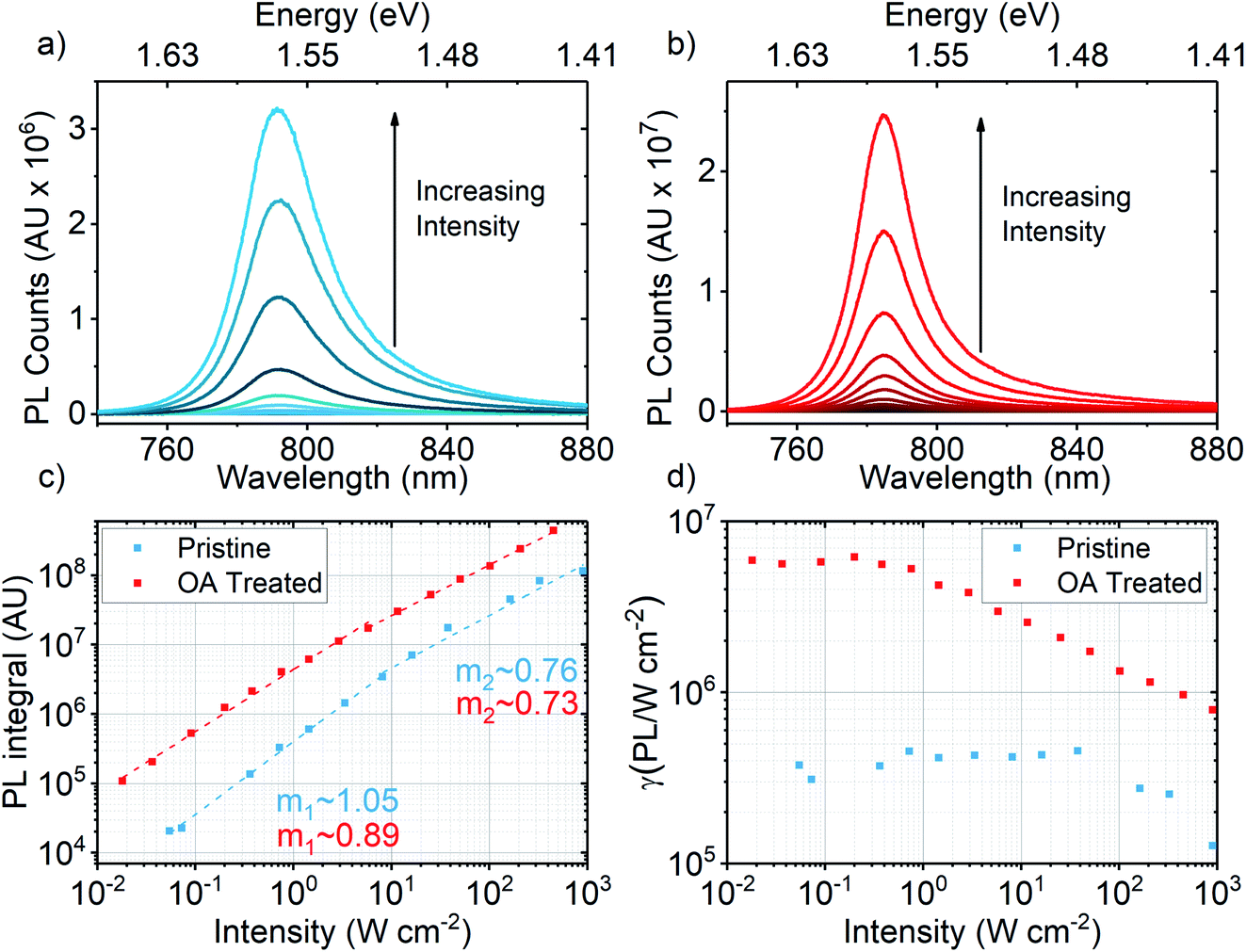 | ||
| Fig. 2 (a) and (b) Raw PL spectra from excitation intensity series of untreated and OA treated MoSe2, respectively; (c) excitation intensity series derived from PL integrals of spectra (a and b) for untreated (blue) and OA treated (red) monolayers; (d) ratio of PL integral to excitation intensity i.e. relative PLQE (γ) as a function of excitation intensity for untreated (blue) and OA treated (red) monolayers. | ||
Fig. 2a shows no noticeable changes in spectral properties with increased excitation intensity in the untreated monolayer. When treated with OA, as shown in Fig. 2b, overall spectral narrowing compared to that of the untreated case was observed; however no additional spectral components are observed, unlike the case of OA treated WS2 which shows strong trion contribution at high excitation intensities.1
Fig. 2c shows a log–log plot of PL integrals as a function of excitation intensity for untreated (blue) and treated (red) samples. The gradients (m) of the series represent the exponent to the power law fit, I = Pm.33 As such, the m values indicate the exciton recombination regimes observed. Fig. 2d shows the ratio of PL to excitation intensity (γ), which serves as a relative PLQE value. At low intensities, the untreated sample shows slight super-linear behaviour (m1 ∼ 1.05), which is indicative of some degree of exciton trapping1 between 0.06 W cm−2 and 0.8 W cm−2. This suggests a lack of non-radiative exciton–exciton annihilation, as given by the little variation in γ ratio values between 1 W cm−2 and 10 W cm−2, albeit with low PLQE. Beyond 10 W cm−2, the trend becomes sublinear (m2 ∼ 0.76), indicating the onset of non-radiative exciton–exciton annihilation.16,20,33,34 However, non-radiative trap assisted recombination processes dominate throughout the series, given the low PLQE of untreated TMD monolayers.1,16,17,20,28–30,32–34
When treated with OA, the emission follows a sub-linear power law exponent m1 of ∼ 0.89 even at lower power, signifying the immediate onset of non-radiative exciton–exciton annihilation, and becomes more drastic at higher excitation intensities where m2 is ∼ 0.73. These trends are reflected in the γ ratio which shows a general gradual reduction between 0.02 W cm−2 and 0.76 W cm−2 before sharply decreasing thereafter due to intensified exciton–exciton annihilation. The immediate exciton–exciton annihilation seen in the OA treated sample is consistent with trap-free exciton diffusion, similar to what has been observed with OA treated WS2.1 The increase in relative PLQE, γ, by an average factor of ∼17 between 0.02 and 0.1 W cm−2 also confirms significant reduction in non-radiative recombination via trap states.
We attempt to characterize the exciton species that contribute to PL of pristine and OA treated MoSe2. Fig. 3a–f show the results obtained from deconvoluting each PL spectrum in the pristine case (Fig. 3a–c) and corresponding OA treated case (Fig. 3d–f). As per previous studies,1,42,43 Gaussian fits (shown in ESI Fig. 3 and 4†) were used to identify the emissive excitonic species in the spectra. Fig. 3a and d show the raw PL spectra of pristine (blue) and OA treated (red) samples taken at 327 W cm−2 and 455 W cm−2, respectively, which lies within the excitation intensity regime for trion emission in OA treated WS2.1 The Gaussian fits X and ζ represent neutral exciton and a low energy spectral component, respectively. Fig. 3b shows the excitation intensity series for X and ζ in pristine MoSe2. We observe that both components exhibit the same power law exponents (m) and (thus) recombination dynamics seen in the ensemble PL excitation intensity series of pristine MoSe2, as shown in Fig. 2c (blue series). Similarly, for the OA treated case shown in Fig. 3e, X and ζ obey the same recombination dynamics seen in the ensemble PL excitation intensity series in Fig. 2c (red line). Fig. 3c and e show the ratio of ζ to X as a function of excitation intensity for pristine and OA treated MoSe2, respectively. In both cases, ζ/X is fairly constant and remains below unity throughout the series. On average, the ζ/X ratio in the OA sample is slightly lower than in the pristine sample. This indicates a slight increase in the proportion of neutral excitons in the OA case compared to that in the pristine case.
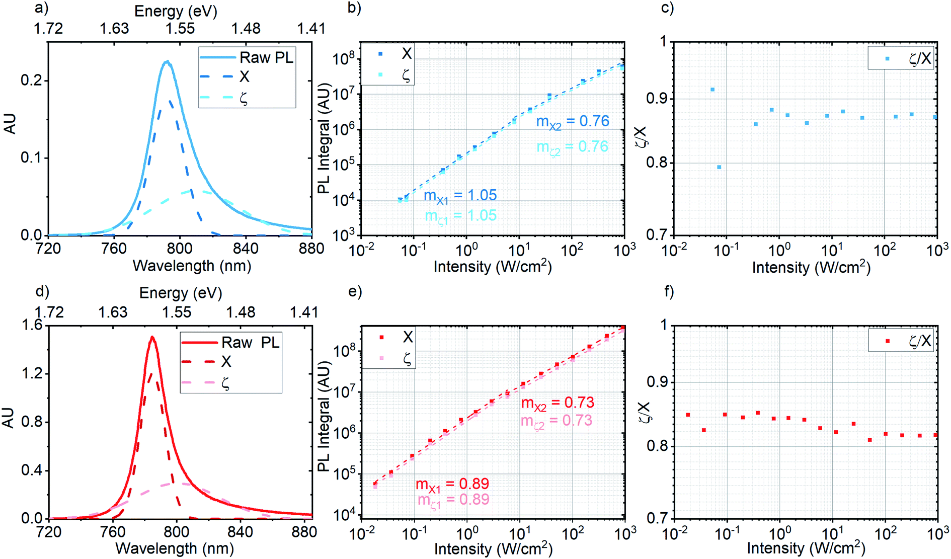 | ||
| Fig. 3 (a) Raw PL spectrum of pristine MoSe2 (blue) taken in the high intensity regime (327 W cm−2). Dashed dark blue and light blue Gaussian fits represent the neutral exciton (X) and a low energy species (ζ), respectively; (b) excitation intensity series of neutral exciton (X) and low energy species (ζ) in pristine MoSe2; (c) ratio of ζ to X as a function of excitation intensity in pristine MoSe2; (d) raw PL spectrum of OA treated MoSe2 (red) taken in the high intensity regime (455 W cm−2). Dashed maroon and pink Gaussian fits represent the neutral exciton (X) and a low energy species (ζ), respectively; (e) excitation intensity series of neutral exciton (X) and low energy species (ζ) in OA treated MoSe2; (f) ratio of ζ to X as a function of excitation intensity in OA treated MoSe2. | ||
The constant ζ/X < 1 ratio in both cases indicates the dominance of neutral excitons compared to low energy species such as trions44 throughout the series. Trions in particular, evolve from the binding of neutral excitons to free photoionized charges and have been characterized in room temperature WS2 PL measurements, which show the growth of a broad and red-shifted low energy feature as a function of increasing excitation intensity.1,42–44 While strong neutral exciton contributions are observed throughout the series, easily discernible trion evolution is not apparent in both pristine and OA treated MoSe2 PL spectra. A recent study on exciton and trion dynamics in MoSe2 concluded that trion formation is suppressed at room temperature due to changes in localisation effects.45 To this end, OA treatment simply improves neutral exciton PL by reducing the density of non-radiative channels which may take the form of trap states caused by chalcogen vacancies. As per the work cited,45 identifying the effects of OA treatment on trion emission in MoSe2 would require low temperature PL studies.
To gain further insights into the exciton dynamics present in OA treated MoSe2, we employ time-resolved photoluminescence (TRPL) microscopy. Fig. 4a shows normalized PL decay signals at room temperature under comparable low intensity 550 nm, 5 MHz pulsed laser excitation. Signals were detected using a visible range single photon avalanche diode (VIS-SPAD) via 750 nm long pass and 900 nm short pass filters, removing laser excitation and collecting MoSe2 PL only. Pulsed excitation intensities used were 0.054 W cm−2 and 0.064 W cm−2 for pristine (blue) and OA treated (red) cases, respectively. Both signals are best described by a bi-exponential decay model (black dashed lines) consisting of fast τ1 and slow τ2 components. The pristine sample (blue) exhibits PL decays with τ1 of ∼ 1.07 ns and τ2 of ∼ 3.06 ns. For the OA treated case (red), PL lifetimes are extended by a factor of 3× and 3.8× vs. the pristine sample for fast and slow decays, respectively, with τ1 of ∼ 3.3 ns and τ2 of ∼ 12.07 ns. The overall increase in PL lifetimes due to OA treatment vs. the pristine case reveals a suppression of non-radiative decay channels.
 | ||
| Fig. 4 (a) Time resolved PL signals of pristine (blue) and OA treated (red) MoSe2 monolayers with bi-exponential decay fits (black dashed lines) measured at comparable pump intensities; 0.054 W cm−2 (pristine sample) and 0.064 W cm−2 (OA sample) using 550 nm, 5 MHz pulsed excitation. (b) Variation of fast PL decay component, τ1 as a function of initial carrier concentration, n0 and pump intensities (W cm−2). | ||
Fig. 4b shows the variation in the fast decay component τ1 as a function of initial carrier concentration n0 over four orders of magnitude. Initial carrier concentrations were computed using openly available MoSe2 steady state absorption data.28 The excitation intensities used fall within the range used for the steady state excitation series shown in Fig. 2c and d. As shown in ESI Fig. 5,† all decays in the series fit a bi-exponential model. The pristine case shows very little variation in τ1 over the range of n0 which indicates exciton trapping. In contrast, OA treated MoSe2 shows a general reduction in τ1 in the n0 range measured. This lies in agreement with the sub-linear trend measured within the same excitation intensity regime shown in Fig. 2c, which indicates the immediate onset of exciton–exciton annihilation at low excitation fluences. Accordingly, the observed reduction in τ1 as a function of n0 in the OA treated sample implies non-trap limited movement of excitons and thus provides further evidence for trap state passivation due to OA treatment. ESI Fig. 6† shows the equivalent comparison for the slow decay component, τ2, for which the pristine case shows a general increase in lifetime as a function of n0 in accordance with trap state filling while the OA treated sample shows a reduction in lifetime as a function of n0.
In summary, steady state PL measurements presented so far show that OA treatment greatly enhances the PL of monolayer MoSe2 and optical quality in terms of emission linewidth and spatial homogeneity of brightness. Steady state excitation intensity dependent PL and TRPL studies reveal trap-free neutral exciton movement in OA treated MoSe2. The observed enhanced PL and trap free exciton annihilation dynamics together support the hypothesis of true defect passivation by OA. In ESI Fig. 7,† we include the PL spectra of pristine and OA treated WSe2 from a single spot on the monolayer to emphasize the versatility of OA treatment.
The exact surface chemistry that gives rise to the observed optical improvement is not fully clear at the moment and future experimental and theoretical studies will be required to understand the underlying mechanism. We note that the Raman spectra of pristine and OA treated MoSe2 in ESI Fig. 8† show no distinguishable structural changes. We however consider that the treatment mechanism would be linked to passivation of chalcogen defects through oleate coordination to Mo dangling bonds. Chemical passivation of these vacancy sites suppresses excitonic trap states, resulting in vastly improved PL efficiency, due to direct band-edge recombination and trap-free exciton movement. In addition, the formation of an OA layer with bulky alkyl chains may provide an insulating encapsulant to the TMD monolayer analogous to hBN encapsulation, resulting in better protection from reactive species formed from atmospheric oxygen and water, and external trap states outside the monolayer from adsorbants, thereby contributing to the observed improvements in optical characteristics. To corroborate the oleate-defect coordination mechanism, we suggest further experiments using an analogous 18 carbon molecule such as cis-9-octadecene.
Finally, to assess the impact of OA treatment on the electronic properties of monolayer MoSe2, we test back-gated field effect transistors. Fig. 5a shows the predominantly n-type transfer characteristics of MoSe2 before OA passivation, consistent with previous reports.46 The as-fabricated devices are then treated with OA under the same conditions as described in the Experimental section. After OA treatment, n-type transfer characteristics are preserved. There is a relatively small threshold voltage (Vth) shift from Vth,Un = 4.8 ± 1 V to Vth,OA = 1.3 ± 2.3 V (Fig. 5b), indicating no substantial change in doping induced by the OA treatment. After OA treatment, the devices consistently show an improved subthreshold swing (SS) from SSUn = 4 ± 0.9 V dec−1 to SSOA = 1 ± 0.1 V dec−1 (Fig. 5c), which indicates a reduction in interface charge trap density and is consistent with the notion of defect passivation by OA. A higher on-state current, due to reduced charge trapping, and larger off-state resistance after OA treatment lead to an improved on–off current ratio up to ∼5 × 10⁴ (Fig. 5d).
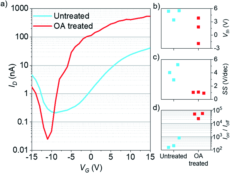 | ||
| Fig. 5 (a) Transfer characteristics of the same back-gated monolayer MoSe2 field effect transistor before (blue) and after (red) OA treatment. (b) Threshold voltage, (c) subthreshold swing, (d) on–off current ratio for three MoSe2 transistors before (blue) and after (red) OA treatment. | ||
Conclusions
In conclusion, we have established OA surface treatment of MoSe2 as an effective means of achieving drastically improved PL yields and trap free PL dynamics, as compared with untreated monolayers. PL statistics reveal that OA treatment yields monolayers of improved optical quality by way of bright spatially homogeneous PL with a narrow spectral linewidth. A steady state excitation intensity dependent PL series reveals significantly improved ‘PLQE’ with trap-free exciton dynamics, which is taken as initial evidence of passivation of non-radiative trap states by OA ligands. Analysis of the excitonic species present in the excitation intensity series verifies dominant neutral exciton recombination in OA treated MoSe2 under low to high excitation intensities. Consistent with improved steady state PL, time resolved PL studies reveal significantly improved PL lifetimes. The reduction in PL lifetimes as a function of initial carrier concentration also indicates trap free exciton movement, which further supports the hypothesis of PL enhancement as a result of ligand passivation. By way of surface chemical interactions between OA and monolayer MoSe2, we hypothesise that the OA ligands coordinate to Mo dangling bonds at Se vacancies, which are known to be exciton trap states, thus passivating them and yielding increased radiative efficiency. The insulating ligands may also protect the monolayer from atmosphere induced doping and surface induced strain, thus acting as an encapsulant, which may also contribute to the PL linewidth narrowing. OA treated MoSe2 based FETs show no significant additional doping. However, we observe a considerable improvement in subthreshold swing with orders of magnitude increase in the on–off ratio, which provides further evidence of trap or defect passivation by OA. In essence, the results show that OA treatment is an effective, simple and versatile ‘wet’ chemistry technique than can improve the PL characteristics of a selenide based TMD. Combined with previous studies on sulphur based TMDs, these results establish the ‘ligand’ based passivation approach as a universal defect treatment protocol for both sulphide and selenide based TMDs.Author contributions
A. O. A. T. prepared samples, performed PL and TRPL measurements, analysed data, wrote manuscript and produced TOC images; J. A.-W. and Y. F. performed transistor preparation, electrical characterization and electronic transport data interpretation; N. G. assembled the TRPL setup; J. X. provided insights into surface chemistry; R. P. assisted in PL data analysis; Z. L. assisted in TOC image preparation.Conflicts of interest
There are no conflicts of interest to declare.Acknowledgements
The authors thank the Winton Program for Physics of Sustainability for financial support. We also acknowledge funding from EPSRC Grants EP/L015978/1, EP/L016087/1, EP/P027741/1, EP/M006360/1, and EP/P005152/1. J. A. W. acknowledges the support of his Research Fellowship from the Royal Commission for the Exhibition of 1851 and Royal Society Dorothy Hodgkin Research Fellowship. Z. L. acknowledges funding from the Swedish Research Council, Vetenskapsrådet 2018-06610. This project has received funding from the European Research Council (ERC) under the European Union's Horizon 2020 Research and Innovation Programme (Grant Agreement 758826).References
- A. O. A. Tanoh, J. Alexander-Webber, J. Xiao, G. Delport, C. A. Williams, H. Bretscher, N. Gauriot, J. Allardice, R. Pandya and Y. Fan, et al., Enhancing Photoluminescence and Mobilities in WS2 Monolayers with Oleic Acid Ligands, Nano Lett., 2019, 19(9), 6299–6307, DOI:10.1021/acs.nanolett.9b02431.
- T. C. Berkelbach and D. R. Reichman, Optical and Excitonic Properties of Atomically Thin Transition-Metal Dichalcogenides, Annu. Rev. Condens. Matter Phys., 2018, 9, 379–396, DOI:10.1146/annurev-conmatphys-033117-054009.
- K. F. Mak and J. Shan, Photonics and Optoelectronics of 2D Semiconductor Transition Metal Dichalcogenides, Nat. Photonics, 2016, 10(4), 216–226, DOI:10.1038/nphoton.2015.282.
- K. F. Mak, C. Lee, J. Hone, J. Shan and T. F. Heinz, Atomically Thin MoS2: A New Direct-Gap Semiconductor, Phys. Rev. Lett., 2010, 105(13), 136805 CrossRef PubMed.
- A. K. Geim and K. S. Novoselov, The Rise of Graphene, Nat. Mater., 2007, 6(3), 183–191, DOI:10.1038/nmat1849.
- S. B. Desai, S. R. Madhvapathy, M. Amani, D. Kiriya, M. Hettick, M. Tosun, Y. Zhou, M. Dubey, J. W. Ager and D. Chrzan, et al., Gold-Mediated Exfoliation of Ultralarge Optoelectronically-Perfect Monolayers, Adv. Mater., 2016, 28(21), 4053–4058, DOI:10.1002/adma.201506171.
- V. Nicolosi, M. Chhowalla, M. G. Kanatzidis, M. S. Strano and J. N. Coleman, Liquid Exfoliation of Layered Materials, Science, 2013, 340(6139), 1226419, DOI:10.1126/science.1226419.
- N. Briggs, S. Subramanian, Z. Lin, X. Li, X. Zhang, K. Zhang, K. Xiao, D. Geohegan, R. Wallace, L. Q. Chen, M. Terrones, A. Ebrahimi, S. Das, J. Redwing, C. Hinkle, K. Momeni, A. van Duin, C. Vin, S. Kar and J. Robinson, A Roadmap for Electronic Grade 2D Materials, 2D Mater., 2019, 6(2), 022001, DOI:10.1088/2053-1583/aaf836.
- A. Chernikov, T. C. Berkelbach, H. M. Hill, A. Rigosi, Y. Li, O. B. Aslan, D. R. Reichman, M. S. Hybertsen and T. F. Heinz, Exciton Binding Energy and Nonhydrogenic Rydberg Series in Monolayer WS2, Phys. Rev. Lett., 2014, 113(7), 076802, DOI:10.1103/PhysRevLett.113.076802.
- H. L. Liu, C. C. Shen, S. H. Su, C. L. Hsu, M. Y. Li and L. J. Li, Optical Properties of Monolayer Transition Metal Dichalcogenides Probed by Spectroscopic Ellipsometry, Appl. Phys. Lett., 2014, 105(20), 201905, DOI:10.1063/1.4901836.
- Q. Wang, K. Kalantar-Zadeh, A. Kis, J. N. Coleman and M. S. Strano, Electronics and Optoelectronics of Two-Dimensional Transition Metal Dichalcogenides, Nat. Nanotechnol., 2012, 7, 699–712, DOI:10.1038/nnano.2012.193.
- C. Palacios-Berraquero, D. M. Kara, A. R. P. Montblanch, M. Barbone, P. Latawiec, D. Yoon, A. K. Ott, M. Loncar, A. C. Ferrari and M. Atatüre, Large-Scale Quantum-Emitter Arrays in Atomically Thin Semiconductors, Nat. Commun., 2017, 8, 15093, DOI:10.1038/ncomms15093.
- Y. You, X. X. Zhang, T. C. Berkelbach, M. S. Hybertsen, D. R. Reichman and T. F. Heinz, Observation of Biexcitons in Monolayer WSe2, Nat. Phys., 2015, 11(6), 477–481, DOI:10.1038/nphys3324.
- M. Barbone, A. R. P. Montblanch, D. M. Kara, C. Palacios-Berraquero, A. R. Cadore, D. De Fazio, B. Pingault, E. Mostaani, H. Li and B. Chen, et al., Charge-Tuneable Biexciton Complexes in Monolayer WSe2, Nat. Commun., 2018, 9(1), 3721, DOI:10.1038/s41467-018-05632-4.
- J. S. Ross, S. Wu, H. Yu, N. J. Ghimire, A. M. Jones, G. Aivazian, J. Yan, D. G. Mandrus, D. Xiao and W. Yao, et al., Electrical Control of Neutral and Charged Excitons in a Monolayer Semiconductor, Nat. Commun., 2013, 4, 1474, DOI:10.1038/ncomms2498.
- M. Amani, D. H. Lien, D. Kiriya, J. Xiao, A. Azcatl, J. Noh, S. R. Madhvapathy, R. Addou, K. C. Santosh and M. Dubey, et al., Near-Unity Photoluminescence Quantum Yield in MoS2, Science, 2015, 350(6264), 1065–1068, DOI:10.1126/science.aad2114.
- S. Roy, W. Choi, S. Jeon, D. H. Kim, H. Kim, S. J. Yun, Y. Lee, J. Lee, Y. M. Kim and J. Kim, Atomic Observation of Filling Vacancies in Monolayer Transition Metal Sulfides by Chemically Sourced Sulfur Atoms, Nano Lett., 2018, 18(7), 4523–4530, DOI:10.1021/acs.nanolett.8b01714.
- S. Barja, S. Refaely-Abramson, B. Schuler, D. Y. Qiu, A. Pulkin, S. Wickenburg, H. Ryu, M. M. Ugeda, C. Kastl and C. Chen, et al., Identifying Substitutional Oxygen as a Prolific Point Defect in Monolayer Transition Metal Dichalcogenides, Nat. Commun., 2019, 10, 3382, DOI:10.1038/s41467-019-11342-2.
- J. Pető, T. Ollár, P. Vancsó, Z. I. Popov, G. Z. Magda, G. Dobrik, C. Hwang, P. B. Sorokin and L. Tapasztó, Spontaneous Doping of the Basal Plane of MoS2 Single Layers through Oxygen Substitution under Ambient Conditions, Nat. Chem., 2018, 10(12), 1246–1251, DOI:10.1038/s41557-018-0136-2.
- D. H. Lien, S. Z. Uddin, M. Yeh, M. Amani, H. Kim, J. W. Ager, E. Yablonovitch and A. Javey, Electrical Suppression of All Nonradiative Recombination Pathways in Monolayer Semiconductors, Science, 2019, 364(6439), 468–471, DOI:10.1126/science.aaw8053.
- D. Rhodes, S. H. Chae, R. Ribeiro-Palau and J. Hone, Disorder in van Der Waals Heterostructures of 2D Materials, Nat. Mater., 2019, 18, 541–549, DOI:10.1038/s41563-019-0366-8.
- W. Zhou, X. Zou, S. Najmaei, Z. Liu, Y. Shi, J. Kong, J. Lou, P. M. Ajayan, B. I. Yakobson and J. C. Idrobo, Intrinsic Structural Defects in Monolayer Molybdenum Disulfide, Nano Lett., 2013, 13(6), 2615–2622, DOI:10.1021/nl4007479.
- S. KC, R. C. Longo, R. Addou, R. M. Wallace and K. Cho, Impact of Intrinsic Atomic Defects on the Electronic Structure of MoS2 Monolayers, Nanotechnology, 2014, 25(37), 375703, DOI:10.1088/0957-4484/25/37/375703.
- O. A. Ajayi, J. V. Ardelean, G. D. Shepard, J. Wang, A. Antony, T. Taniguchi, K. Watanabe, T. F. Heinz, S. Strauf and X. Y. Zhu, Approaching the Intrinsic Photoluminescence Linewidth in Transition Metal Dichalcogenide Monolayers, 2D Mater., 2017, 4(3), 031011, DOI:10.1088/2053-1583/aa6aa1.
- F. Cadiz, E. Courtade, C. Robert, G. Wang, Y. Shen, H. Cai, T. Taniguchi, K. Watanabe, H. Carrere and D. Lagarde, et al., Excitonic Linewidth Approaching the Homogeneous Limit in MoS2-Based van der Waals Heterostructures, Phys. Rev. X, 2017, 7(2), 021026, DOI:10.1103/PhysRevX.7.021026.
- E. Courtade, B. Han, S. Nakhaie, C. Robert, X. Marie, P. Renucci, T. Taniguchi, K. Watanabe, L. Geelhaar and J. M. J. Lopes, et al., Spectrally Narrow Exciton Luminescence from Monolayer MoS2 and MoSe2 Exfoliated onto Epitaxially Grown Hexagonal BN, Appl. Phys. Lett., 2018, 113(3), 032106, DOI:10.1063/1.5033554.
- Y. Hoshi, T. Kuroda, M. Okada, R. Moriya, S. Masubuchi, K. Watanabe, T. Taniguchi, R. Kitaura and T. Machida, Suppression of Exciton-Exciton Annihilation in Tungsten Disulfide Monolayers Encapsulated by Hexagonal Boron Nitrides, Phys. Rev. B, 2017, 95(24), 2414013, DOI:10.1103/PhysRevB.95.241403.
- S. Mouri, Y. Miyauchi and K. Matsuda, Tunable Photoluminescence of Monolayer MoS2via Chemical Doping, Nano Lett., 2013, 13(12), 5944–5948, DOI:10.1021/nl403036h.
- N. Peimyoo, W. Yang, J. Shang, X. Shen, Y. Wang and T. Yu, Chemically Driven Tunable Light Emission of Charged and Neutral Excitons in Monolayer WS2, ACS Nano, 2014, 8(11), 11320–11329, DOI:10.1021/nn504196n.
- W. Su, H. Dou, J. Li, D. Huo, N. Dai and L. Yang, Tuning Photoluminescence of Single-Layer MoS2 Using H2O2, RSC Adv., 2015, 5(101), 82924–82929, 10.1039/c5ra12450f.
- D. Kiriya, Y. Hijikata, J. Pirillo, R. Kitaura, A. Murai, A. Ashida, T. Yoshimura and N. Fujimura, Systematic Study of Photoluminescence Enhancement in Monolayer Molybdenum Disulfide by Acid Treatment, Langmuir, 2018, 34(35), 10243–10249, DOI:10.1021/acs.langmuir.8b01425.
- J. H. Park, A. Sanne, Y. Guo, M. Amani, K. Zhang, H. C. P. Movva, J. A. Robinson, A. Javey, J. Robertson and S. K. Banerjee, et al.,Defect Passivation of Transition Metal Dichalcogenides via a Charge Transfer van der Waals Interface, Sci. Adv., 2017, 3(10), 1701661, DOI:10.1126/sciadv.1701661.
- M. Amani, P. Taheri, R. Addou, G. H. Ahn, D. Kiriya, D. H. Lien, J. W. Ager, R. M. Wallace and A. Javey, Recombination Kinetics and Effects of Superacid Treatment in Sulfur- and Selenium-Based Transition Metal Dichalcogenides, Nano Lett., 2016, 16(4), 2786–2791, DOI:10.1021/acs.nanolett.6b00536.
- H. Kim, D. H. Lien, M. Amani, J. W. Ager and A. Javey, Highly Stable Near-Unity Photoluminescence Yield in Monolayer MoS2 by Fluoropolymer Encapsulation and Superacid Treatment, ACS Nano, 2017, 11(5), 5179–5185, DOI:10.1021/acsnano.7b02521.
- A. J. Goodman, A. P. Willard and W. A. Tisdale, Exciton Trapping Is Responsible for the Long Apparent Lifetime in Acid-Treated MoS2, Phys. Rev. B, 2017, 96(12), 121404(R), DOI:10.1103/PhysRevB.96.121404.
- H. M. Bretscher, Z. Li, J. Xiao, D. Y. Qiu, S. Refaely-Abramson, J. Alexander-Webber, A. O. A. Tanoh, Y. Fan, G. Delport and C. Williams, et al., Rational Passivation of Sulfur Vacancy in Two-Dimensional Transition Metal Dichalcogenides, ACS Nano, 2021, 15(5), 8780–8789, DOI:10.1021/acsnano.1c01220.
- H. V. Han, A. Y. Lu, L. S. Lu, J. K. Huang, H. Li, C. L. Hsu, Y. C. Lin, M. H. Chiu, K. Suenaga and C. W. Chu, et al., Photoluminescence Enhancement and Structure Repairing of Monolayer MoSe2 by Hydrohalic Acid Treatment, ACS Nano, 2016, 15(7), 4374–4380, DOI:10.1021/acsnano.5b06960.
- H. Kim, G. H. Ahn, J. Cho, M. Amani, J. P. Mastandrea, C. K. Groschner, D. H. Lien, Y. Zhao, J. W. Ager, M. C. Scott, D. C. Chrzan and A. Javey, Synthetic WSe2 Monolayers with High Photoluminescence Quantum Yield, Sci. Adv., 2019, 5(1), eaau4728, DOI:10.1126/sciadv.aau4728.
- P. Johari and V. B. Shenoy, Tuning the Electronic Properties of Semiconducting Transition Metal Dichalcogenides by Applying Mechanical Strains, ACS Nano, 2012, 6(6), 5449–5456, DOI:10.1021/nn301320r.
- H. Li, J. Wu, X. Huang, G. Lu, J. Yang, X. Lu, Q. Xiong and H. Zhang, Rapid and Reliable Thickness Identification of Two-Dimensional Nanosheets Using Optical Microscopy, ACS Nano, 2013, 7(11), 10344–10353, DOI:10.1021/nn4047474.
- K. Momma and F. Izumi, VESTA 3 for Three-Dimensional Visualization of Crystal, Volumetric and Morphology Data, J. Appl. Crystallogr., 2011, 44(6), 1272–1276, DOI:10.1107/S0021889811038970.
- I. Paradisanos, S. Germanis, N. T. Pelekanos, C. Fotakis, E. Kymakis, G. Kioseoglou and E. Stratakis, Room Temperature Observation of Biexcitons in Exfoliated WS2 Monolayers, Appl. Phys. Lett., 2017, 110(19), 193102, DOI:10.1063/1.4983285.
- K. Wei, Y. Liu, H. Yang, X. Cheng and T. Jiang, Large Range Modification of Exciton Species in Monolayer WS2, Appl. Opt., 2016, 55(23), 6251, DOI:10.1364/AO.55.006251.
- A. A. Mitioglu, P. Plochocka, J. N. Jadczak, W. Escoffier, G. L. J. A. Rikken, L. Kulyuk and D. K. Maude, Optical Manipulation of the Exciton Charge State in Single-Layer Tungsten Disulfide, Phys. Rev. B: Condens. Matter Mater. Phys., 2013, 88(24), 245403, DOI:10.1103/PhysRevB.88.245403.
- T. Godde, D. Schmidt, J. Schmutzler, M. Aßmann, J. Debus, F. Withers, E. M. Alexeev, O. Del Pozo-Zamudio, O. V. Skrypka, K. S. Novoselov, M. Bayer and A. I. Tartakovskii, Exciton and Trion Dynamics in Atomically Thin MoSe2 and WSe2: Effect of Localization, Phys. Rev. B, 2016, 94(16), 165301, DOI:10.1103/PhysRevB.94.165301.
- S. Larentis, B. Fallahazad and E. Tutuc, Field-Effect Transistors and Intrinsic Mobility in Ultra-Thin MoSe2 Layers, Appl. Phys. Lett., 2012, 101(22), 223104, DOI:10.1063/1.4768218.
Footnote |
| † Electronic supplementary information (ESI) available: Spectral deconvolution of OA treated MoSe2 PL spectra using Gaussian fits; all time resolved PL signals for pristine and OA treated MoSe2 including bi-exponential decay fits; variation of slow PL decay components with initial carrier concentration; and Raman spectra of pristine and OA treated MoSe2 on a glass slide. See DOI: 10.1039/d0na01014f. All data underlying this publication are available via the link: https://doi.org/10.17863/CAM.71364 |
| This journal is © The Royal Society of Chemistry 2021 |