
 Open Access Article
 This Open Access Article is licensed under a Creative Commons Attribution-Non Commercial 3.0 Unported Licence
Deterministic synthesis of Cu9S5 flakes assisted by single-layer graphene arrays†
A.
Portone
 a,
L.
Bellucci
a,
D.
Convertino
bd,
F.
Mezzadri
fg,
G.
Piccinini
bc,
M. A.
Giambra
e,
V.
Miseikis
bd,
F.
Rossi
f,
C.
Coletti
bd and
F.
Fabbri
*a
a,
L.
Bellucci
a,
D.
Convertino
bd,
F.
Mezzadri
fg,
G.
Piccinini
bc,
M. A.
Giambra
e,
V.
Miseikis
bd,
F.
Rossi
f,
C.
Coletti
bd and
F.
Fabbri
*a
aNEST, Istituto Nanoscienze – CNR, Scuola Normale Superiore, Piazza San Silvestro 12, 56127 Pisa, Italy. E-mail: filippo.fabbri@nano.cnr.it
bCNI@NEST, Istituto Italiano di Tecnologia, Piazza San Silvestro 12, 56127 Pisa, Italy
cScuola Normale Superiore, Piazza San Silvestro 12, 56127 Pisa, Italy
dGraphene Labs, Istituto Italiano di Tecnologia, Via Morego 30, 16163 Genova, Italy
eCNIT, Sant'Anna, Via G. Moruzzi 1, Pisa, 56124, Italy
fIMEM-CNR, Parco Area delle Scienze 37/a, Parma, 43124, Italy
gDepartment of Chemistry, Life Sciences and Environmental Sustainability, University of Parma, Parco Area delle Scienze 11/A, 43124 Parma, Italy
First published on 2nd February 2021
Abstract
The employment of two-dimensional materials, as growth substrates or buffer layers, enables the epitaxial growth of layered materials with different crystalline symmetries with a preferential crystalline orientation and the synthesis of heterostructures with a large lattice constant mismatch. In this work, we employ single crystalline graphene to modify the sulfurization dynamics of copper foil for the deterministic synthesis of large-area Cu9S5 crystals. Molecular dynamics simulations using the Reax force-field are used to mimic the sulfurization process of a series of different atomistic systems specifically built to understand the role of graphene during the sulphur atom attack over the Cu(111) surface. Cu9S5 flakes show a flat morphology with an average lateral size of hundreds of micrometers. Cu9S5 presents a direct band-gap of 2.5 eV evaluated with light absorption and light emission spectroscopies. Electrical characterization shows that the Cu9S5 crystals present high p-type doping with a hole mobility of 2 cm2 V−1 s−1.
Introduction
Since the discovery of graphene,1,2 a prototypical two-dimensional (2D) material, great efforts have been made to investigate low-dimensional materials. Applications of graphene-based devices in electronics,3,4 valleytronics,5 optoelectronics6,7 and photonics6,8 have made 2D materials one of the most active areas of research in the last decade.Graphene has also been widely used as a growth substrate for the synthesis of different classes of materials and nanostructures. In particular, graphene has been employed as a substrate in the synthesis of InAs nanowires with preferential orientation of NW facets9,10 or in the production of double-heterojunction InAs/Gr/InAs nanowires.11 Similar results were obtained in the synthesis of ZnO nanorods on graphene resulting in a high vertical alignment with an epitaxial relationship between ZnO and graphene.12 Recently a new approach has been demonstrated in the growth of 3D crystalline materials using a 2D material as a buffer layer in the growth process.13–15 This process has been successfully employed in the development of low dislocation density GaN based light emitting diodes (LEDs) on graphene coated ZnO.16 Similarly, AlGaN, a deep-UV LED with promising light emission properties, has been realized on high quality AlN/Gr/AlN structures, where graphene plays a fundamental role in the synthesis of a high quality AlN substrate.17 A similar strategy has been developed for the heteroepitaxy of III–V materials as the growth on graphene-coated substrates enables spontaneous relaxation of the epilayer before the accumulated elastic energy created by the lattice mismatch induces misfit dislocations. This approach has been demonstrated on low misfit strain InGaP on GaAs (0.74% misfit strain) and on high misfit strain GaP on GaAs (3.7% misfit strain).14
In the case of the synthesis of 2D layered materials or three-dimensional (3D) crystalline layers on top of layered materials this particular method has been identified as van der Waals epitaxy (vdWE) by Koma.18
vdWE enables the epitaxial growth of layered materials with different crystalline symmetries to the substrate. In addition, this method can be used even when the lattice constant mismatch is as high as 50% and no excessive strain exists in the epitaxial layer. The main advantages of vdWE include rotational alignment with the substrate, strain-free growth, and no misfit dislocations despite the significant lattice mismatch.19
The vdWE approach includes two different configurations. The first is the growth of 2D layered materials onto 3D crystal substrates, which have saturated dangling bonds on their clean surfaces. Then, a single-crystalline film of a layered material can be heteroepitaxially grown on such a dangling-bond-terminated surface via van der Waals-like weak force. For example, layered material (NbSe2, MoSe2, GaSe, InSe) films have been grown on such saturated dangling bond surfaces as H-terminated Si(111), S or Se-terminated GaAs(111), and F-terminated CaF2(111).19 The second layout of the vdWE is the synthesis of a layered material onto another layered substrate, which has no dangling bond on its cleaved surface. This approach has been widely employed in the growth of transition metal dichalcogenides (TMDs) on top of graphene20,21 or mica substrates.22,23 For instance, the CVD synthesis of WS2 monolayers on top of epitaxial graphene or of CVD graphene has demonstrated a preferential orientation between 0° and 60° of monolayer WS2.24–27 Another example of this configuration is the synthesis of a mono- or few layer metal monochalcogenide on top of another TMD material:19 the CVD synthesis of monolayer GaSe on monolayer MoSe2, despite a large lattice misfit, results in bilayer heterojunctions with atomically sharp interfaces.28 Even in the case of two-dimensional monoelemental materials the vdWE method has been successful in the synthesis of few layer antimonene29 or tellurium30 on mica and silicene on graphite.31,32 In this work, we utilize graphene single-crystals to modify the sulfurization dynamics of copper foil for the deterministic synthesis of large-area Cu9S5 crystals. We are able to synthesize Cu9S5 flakes (also known as digenite) with a lateral size of more than 50 μm. The graphene crystals are completely etched during the growth process. Comprehensive analysis of the optical and electrical properties is carried out after dry stamp transfer of the Cu9S5 crystals. In particular, the evaluation of the optical band-gap has been carried out on the crystals revealing that the Cu9S5 has an optical direct band-gap of about 2.5 eV. The electrical characterization shows that the Cu9S5 crystals present high p-type doping with a hole mobility of 2 cm2 V−1 s−1.
Experimental
The growth process was performed within a 2.5-inches horizontal hot-wall furnace (Lenton PTF). The furnace comprises a central hot-zone, where the graphene topped copper foil crucible was placed, and an inlet zone, where the S powder (500 mg) was positioned and heated by a resistive belt.Graphene single crystal arrays with a lateral size of about 100 μm are synthesized via CVD on electropolished copper (Cu) foils (Alfa Aesar, 99.8%) following the procedure described by Miseikis et al.33,34 Graphene was then synthesized at a temperature of 1060 °C inside a cold-wall CVD system (Aixtron BM) flowing methane, hydrogen, and argon.
Scanning electron microscopy (SEM) was performed to study the morphology of Cu2S flakes. The SEM analysis is carried out using an in-lens detector on a Zeiss Merlin FEG-SEM microscope, with an accelerating voltage of 5 kV and an electron current of 96 pA, in order to minimize the damage due to the electron beam irradiation.
AFM analysis was performed with an AFM+ from Anasys Instruments, operated in tapping-mode. AFM micrographs were analysed using the software Gwyddion 2.45.
Raman spectroscopy and mapping were carried out with a Renishaw InVia system, equipped with a confocal microscope, a 473 nm excitation laser and a 2400 line per mm grating (spectral resolution 0.5 cm−1). All the analyses were performed with the following parameters: excitation laser power, 0.5 mW and acquisition time for each spectrum, 10 s. The maps were obtained with the same acquisition parameters and a pixel size of 2 μm × 2 μm. PL spectroscopy was performed with the same system using the 473 nm excitation laser. All the spectra were obtained with the following parameters: excitation laser power, 0.5 mW and acquisition time for each spectrum, 30 s.
Ultraviolet-visible (UV-Vis) absorbance spectra were collected from Cu9S5 flakes transferred on a thick PDMS film by using a Lambda 950 spectrophotometer (Perkin Elmer Inc.) equipped with deuterium and tungsten halogen light sources, a double holographic grating monochromator and a high-sensitivity photomultiplier tube. Spectra were acquired in the wavelength range from 250 nm to 650 nm with a spectral resolution of 1 nm.
Energy Dispersive X-ray (EDX) spectroscopy and mapping were performed on a JEOL JEM-2200FS Transmission Electron Microscope operated at 200 kV in scanning mode (STEM, spot size 2 nm), using an Oxford XPLORE detector with drift correction. The samples were deposited by drop-casting on carbon coated nickel grids.
I–V curves and Hall measurements were carried out at room temperature with an Ecopia HMS-3000 Hall measurement system. Cu9S5 flakes are brought into contact by means of silver paste and the tip of the manipulator is positioned on the PDMS surface covered with a drop of silver paste. Due to the extreme brittleness of digenite, the possible force applied by the manipulator can break the flake. The I–V curves are obtained applying a bias from −0.5 V to 0.5 V with a step of 50 mV. In the case of Hall measurements, the probe current was selected such that the voltage signal was 0.2 V with a magnetic field of 0.37 T.
Powder X-ray diffraction data were acquired using a Rigaku Smartlab XE diffractometer. The CuKα incident beam was parallelized through a parabolic mirror in order to limit the sample roughness effects on the peak shape and position. Measurements were carried out in the Bragg–Brentano configuration with 5° soller slits both on the incident and diffracted beam. An HyPix3000 detector was operated in 1D mode. Samples were placed on a zero-background sample holder and data were collected in the 10°–80° 2θ range with 0.01° steps and 2° min−1 speed.
Molecular dynamics simulation details
MD simulations were carried out using LAMMPS.35 ReaxFF parameters to treat Cu/S/C/H were taken from the work of Yeon et al.36 Interactions between argon and Cu/S/C/H atoms were treated exploiting the Lennard-Jones (LJ) potential. Parameters were taken from the Universal Force Field37,38 (UFF). Lorentz–Berthelot mixing rules were applied to calculate cross interactions. LJ interactions were truncated applying a cut-off of 1 nm. For structural details see Fig. 2 and S6.† All simulations were performed by using a triclinic simulation box (a = b = 2.55 nm, c = 7 nm, α = β = 90°, γ = 120°) applying periodic boundary conditions (PBCs) in all directions and by using the same computational protocol. A preliminary minimization employing the conjugate-gradient (CG) algorithm as implemented in LAMMPS was performed for all the systems. Optimized structures were used to initialize the MD simulations. The initial temperature was set to 300 K. All systems were then heated to 1000 K in 2 ps and equilibrated for 12 ps reassigning velocities every 2 ps. Systems were indeed relaxed by means of 1 ns of MD simulation at constant temperature (NVT ensemble). Finally, the relaxed systems were annealed to 300 K in 100 ps of MD simulations and minimized with CG. Temperature was controlled by using the canonical sampling through velocity rescaling (CSVR) thermostat39 with a time constant of 0.1 ps, whereas the motion of the atoms was integrated with a time step of 0.2 fs. The binding energy per carbon atom (Eb) is obtained by subtracting the energy of the Cu slab (ECuS) and of the graphene layer (EGr) from the total energy of the system (ETot) and dividing by the number of carbon atoms (NC) of the graphene layer:40
Visual inspections of MD trajectories and figures were performed with VMD1.9.3.41
Results and discussion
Fig. 1a shows a schematic illustration of the synthesis reactor, a furnace with two temperature zones. The sulphur boat is positioned in a low temperature zone, while the graphene array covered Cu foil33 is placed in the high temperature zone. The sulphur precursor (blue dashed line), substrate temperature (blue full line) and the Ar flow (light blue full line) profiles are shown in Fig. 1b. After 30 minutes purging (the pressure in the growth chamber reaches P = 1 × 10⁻³ mbar), the substrate temperature is increased to 750 °C with a 40 °C min−1 ramp. During the temperature ramp-up the argon flow is increased to 500 sccm (P = 3 mbar) in order to raise the chamber pressure, avoiding the evaporation of the sulphur powder. The uncontrolled evaporation of the sulphur during the temperature ramp-up can give rise to the formation of low-temperature phases of Cu–S compounds, such as chalcocite.42 Once the set point temperature has been reached, the Ar flow is decreased down to 250 sccm (P = 1 mbar) and the S powder is separately heated to 200 °C using a heating belt, causing rapid evaporation of the sulphur. Raman spectroscopy is employed to assess the crystalline structure of the Cu–S compounds. After the synthesis process the Raman spectrum, measured on the original locations of the graphene crystals, presents a sharp peak at ∼469.5 cm−1 (Fig. 1c), attributed to the A1g peak of Cu9S5 (digenite).43 It is worth noting that the Raman shift of the A1g has been widely employed to identify the crystal structure of Cu–S compounds. In fact monoclinic Cu2S (low chalcocite)44 and hexagonal Cu2S (high chalcocite)45 present the A1g peak at 471.2 cm−1 and at 472 cm−1, respectively, while the peak is positioned at 474 cm−1 in the case of hexagonal CuS (covelite).46–48 No Raman spectral features of graphene such as D or G peaks are observable, indicating complete removal of the graphene crystals, by chemical etching or mechanical detachment (Fig. S1†).33,49 An enlargement of the A1g peak is reported in the inset of Fig. 1c. The characterization of the graphene on copper is reported in Fig. S2.† The Raman and the XRD spectra of the material outside the flakes are reported in Fig. S3 of the ESI,† and they show that it is composed of a mixture of Cu9S5 (digenite) and CuS (covelite). The Raman map is shown in Fig. S4,† confirming the removal of graphene on the overall area of the Cu9S5 flake.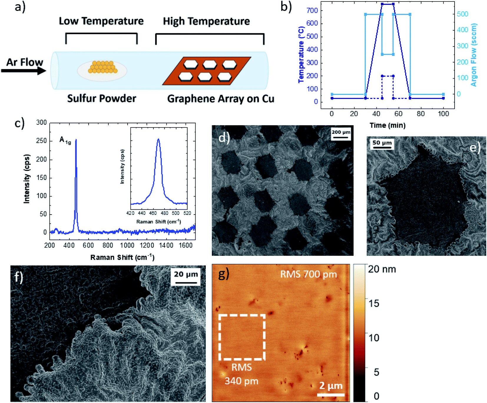 | ||
| Fig. 1 (a) Sketch of the synthesis reactor, with an indication of the disposition of the sulfur precursor and of the graphene array on copper foil. (b) Temperature of the sulfur precursor (blue dashed line) and of the growth substrate (blue full line) and Ar carrier flow (light blue full line) during the growth process. (c) Raman spectrum inside the Cu9S5 flakes. The inset presents an enlargement of the A1g peak. (d)–(f) SEM images of the Cu9S5 flake arrays, a single flake and a high magnification of the flake morphology. (g) AFM analysis of the Cu9S5 flake. | ||
Fig. 1d shows the SEM image of a 4 × 4 array of Cu9S5, as identified by Raman analysis. Indeed, it is clear from the micrograph that the graphene crystals assist the growth of Cu9S5, as the hexagonal shape of the graphene flake is transferred to the Cu9S5compounds. It is possible to note the presence of cracks outside the array related to the extreme brittleness of digenite, as previously reported.50 The SEM image of a single flake is reported in Fig. 1e. The high magnification SEM image of a Cu9S5 flake reveals that the areas where the graphene crystal is present are recessed with respect to the surrounding dendritic areas. The SEM analysis reveals that the flakes are composed of grains with different sizes. In order to evaluate the morphology of the grains comprising the Cu9S5 flake, atomic force microscopy (AFM) is carried out. The average root mean square (RMS) of the whole area is 700 pm meanwhile the micrometric areas, highlighted by the white square, present a lower RMS (340 pm). The Cu9S5 flake shows a flat surface in comparison with CuXS compounds, obtained with similar strategies.50 The line profile of nanometric pits is reported in Fig. S5.† The morphological analysis suggests that the presence of graphene crystals affects the growth direction of the underlying Cu9S5, resulting in the alignment of the basal plane of graphene and of Cu9S5, albeit the graphene is completely removed, by chemical etching or mechanical detachment, during the growth process. This hypothesis is supported by the extremely low RMS and by the recessed morphology of the Cu9S5 flakes. In fact, the raised dendritic morphology of the surrounding areas outside the flakes is probably due to a random orientation of the Cu9S5 and CuS phases. A similar effect was previously reported in the case of the sulfurization of copper thin films, where the increase of the copper thickness results in the synthesis of vertically aligned β-Cu2S lamellas.51
Until now the synthesis of Cu9S5 has been carried out mainly with solution processes.52–54 Recently a novel method, similar to that presented in this work, is reported for the high yield synthesis of bulk Cu9S5 by vapour phase sulfurization of copper foil.50
To characterize the formation of Cu9S5 flakes at the molecular-atomistic level, molecular dynamics (MD) simulations were performed considering different model systems composed of a copper Cu(111) surface exposed to a sulphur/argon mixture or screened from the S/Ar atoms by single layer graphene or by graphene ribbons (see Fig. 2 and S6†). For this purpose, we used the empirical reactive force-field55 (ReaxFF) as implemented in the LAMMPS software package,56,57 exploiting the recent parametrization developed for Cu/S/C/H.36 The use of such a force-field allows us to empirically model reactive events occurring during the sulfurization process through a bond-order formalism. All the systems were treated as periodic by applying a periodic boundary condition scheme (see the Experimental section). In this framework, we investigated the role of graphene on top of the Cu(111) surface during the initial stage (about 1 ns) of the sulfurization process that eventually leads to the synthesis of Cu9S5. All simulations were initialized and relaxed at constant temperature (1000 K) for 1 ns employing the same computational protocol (see methods). The relaxed structures were then optimized through a minimization protocol (see methods) and are shown in Fig. 2. The trajectories of the MD simulations were then inspected and used to grasp the response of the systems to the chemical attack of sulphur (S). The Cu(111) surface completely covered by graphene during sulphur attack is stable (Fig. 2a). The binding energy (Eb) per carbon atom, i.e. the interaction energy between graphene and the metal surface was about −40 meV, which is in agreement with the values evaluated at the density functional level of theory;40 graphene adheres to the surface and being chemically inert protects the Cu atoms from the chemical attack. Sulphur atoms in excess remain in the box simulation, occasionally forming small chains or cyclic molecules.58,59 The uncovered Cu(111) is attacked by S atoms during the MD simulation (Fig. 2b). The Cu atoms of the first layer are extruded from the surface and react with chemisorbed sulphur atoms. Reactions can also occur among sulphur atoms, leading to the formation of small S chains and S–S bonds interconnecting Cu atoms (see Movie 1†). This is likely disadvantageous for further S attack and the diffusion of S into the inner layers. The formation of these sulphur chains reminds of the structure of copper mixed monosulphide/disulphide (e.g., CuS or CuS2) that differs from digenite, which contains only isolated sulphide anions, by the presence of direct S–S bonds (Fig. S7†). The behaviour of the surfaces covered with graphene ribbons is consistent with that observed in the two previous cases. Graphene ribbons, protecting Cu from the S attack, remain attached to the metal surface (Fig. 2c). During the simulation, some sulphur atoms approach the hydrogenated edges and partially intercalate between the graphene/Cu interface. However, no sulphur atoms crossed the interface, as sulphur intercalation is hindered by the presence of graphene adhering to the surface. This means that the intercalation process is a slow process regulated by an activation energy (e.g., the energy due to the partial detachment and/or large deformation of the edges of the graphene) which prevents its observation in the time scale of standard MD simulations.60 The relaxed structures of two systems with different numbers of intercalated sulfur atoms are shown in Fig. 2d and in Fig. 2e. During the simulation large rearrangements of Cu and S atoms occur. Graphene remains attached to the surface, eventually driving the intercalation of single sulphur atoms over the Cu(111) surface. The presence of graphene prevents the intercalation of sulphur chains and shields the intercalated S atoms from the S/Ar mixture, disadvantageous for uncontrolled formation of S–S bonds or further S chains (see Movie 2†). Therefore, during the sulfurization process, graphene promotes the formation of a more ordered morphology of the surface (compare Fig. 2b with Fig. 2d and e). Remarkably, during the relaxation of the system with the graphene covered Cu(111) surface, no sulphur chains and S–S bonds form and the sulphur atoms are evenly distributed among Cu atoms of the metal surface. The bond energy for the carbon atoms decreases as the number of S increases, being −17 meV for the system shown in Fig. 2d and −19 meV for the system in Fig. 2e. The intercalation of sulphur therefore favours the detachment of graphene. However, during the MD simulations it was not possible to observe the release of graphene due to the pressure of the gas phase (i.e. the Ar/S mixture) which acts on the periodic surface of the graphene, which in this specific case prevents its detachment.
 | ||
| Fig. 2 Representative snapshots of the model systems used to study the sulfurization process of Cu (111) exposed to the sulphur/argon mixture in the presence of various types of graphene coverages. (a) Cu(111) completely covered with graphene. (b) Cu(111) completely exposed to the gas mixture. (c) Cu(111) partially covered by graphene ribbons. (d) System with 36 sulfur atoms intercalated between the metal surface and graphene. In the inset of (d) shown an alternative view highlighting the arrangement of the sulphur atoms on top of the Cu(111). (e) System with 18 sulphur atoms intercalated between the metal surface and graphene. | ||
In order to analyse the Cu9S5 flakes we employ a two-step PDMS stamp process in order to transfer only the flakes. The transfer process (Fig. 3a) is based on a PDMS thick film that is applied to the surface of the substrate and gently pressed. Due to the extreme brittleness of digenite50 and the recessed morphology of the Cu9S5 flakes when the PDMS film is peeled off, the surrounding material remains attached to the film while the flakes remain on the residual copper foil substrate. With a second step, similar to the first one, it is possible to detach the flakes from the residual copper foil. Then, the flakes are analysed on the PDMS substrate or they are detached by gentle sonication in isopropanol. The optical image of the transferred flakes is reported in Fig. S8 of the ESI.† In order to evaluate the thickness of the Cu9S5 flake, we measure the thickness of the pristine copper foil, after the synthesis of graphene, and after the transfer of the sulfurized layer. The pristine copper foil is 25 μm thick, and it decreases to 8 μm due to the electrochemical polishing, necessary for the graphene synthesis. The thickness of the residual copper foil, obtained by stylus profilometry, decreases down to 5 μm after the sulfurization process, revealing that the thickness of the transferred sulfurized layer is about 3 μm. The flakes can be transferred on a nickel TEM grid in order to study the structural and compositional properties. The low magnification TEM image is reported in Fig. 3b, revealing that the flakes are damaged during the transfer process and they are not electron transparent due to the micrometric thickness. The TEM-EDX spectrum (Fig. 3c) presents the characteristic S and Cu peaks. Additional peaks are due to the nickel of the TEM grid and the Fe and Co of the TEM sample holder; no other impurity elements are detected. Elemental maps (Fig. 3d) show a continuous distribution of S and Cu, confirming that the growth process allows a good spatial uniformity of the sample.
 | ||
| Fig. 3 (a) Schematic of the two-step PDMS stamp transfer, (b) low magnification TEM image. (c) EDS spectrum and (d) EDS maps of copper (cyan) and sulfur (red). | ||
After the transfer onto the PDMS thick film (inset of Fig. 4a), we carried out optical and electrical characterization of the Cu9S5 crystals. In general, the bandgap of CuXS compounds can vary from 1.2 eV to 2.5 eV, depending on different factors, such as the crystalline phase, the stoichiometry, the nanostructure.61 In particular, bulk Cu9S5 (digenite phase) has a direct bandgap of 2.5 eV,50 however the optical bandgap of nanomaterials is deeply linked with their morphology, in fact the reported bandgap of Cu9S5 varies from 1.73 eV (film)52 to 1.93 eV (nanocube)62 and 2.1 eV for 2D triangular flakes.43
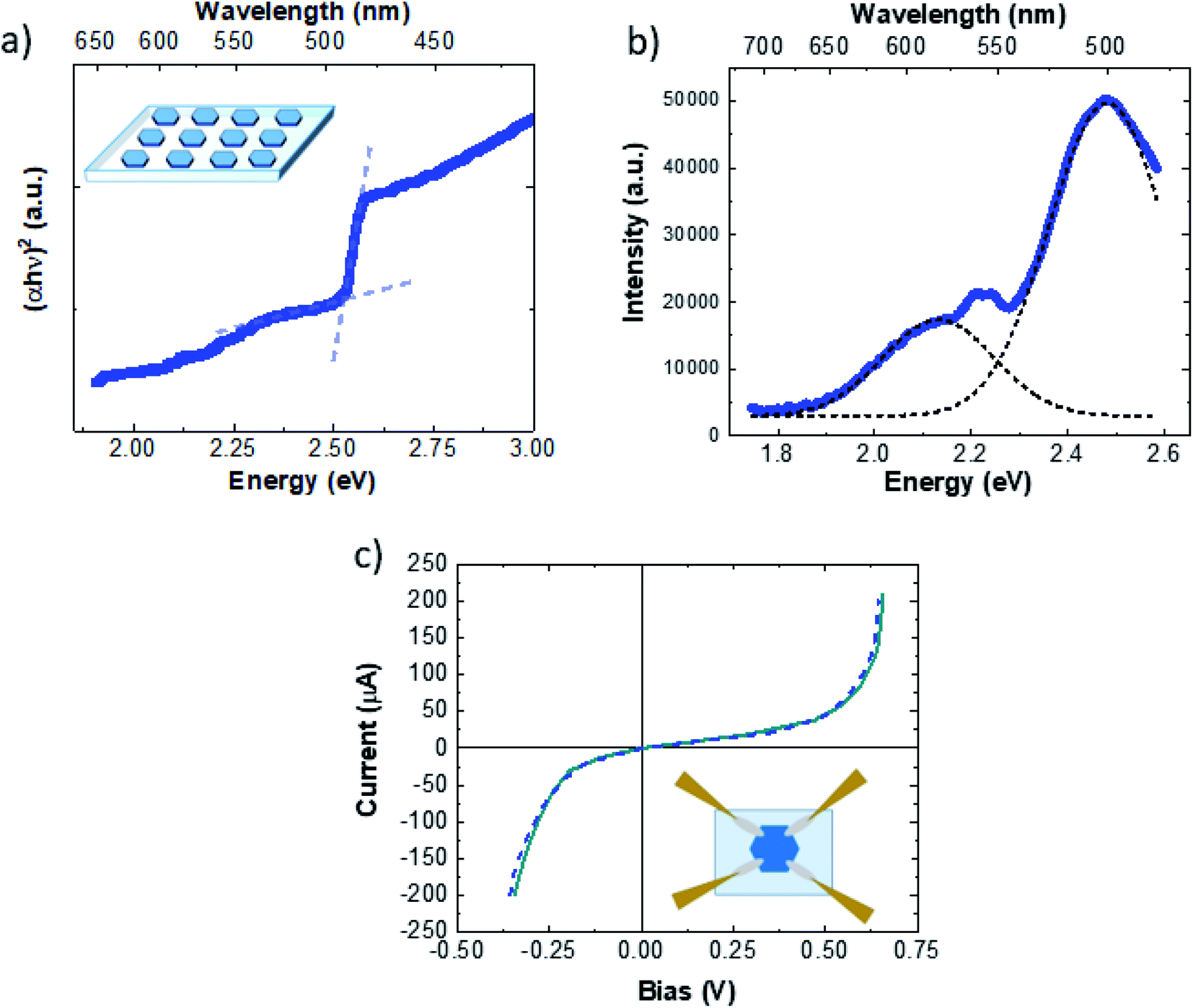 | ||
| Fig. 4 (a) Tauc plot of Cu9S5 flakes on the PDMS thick film. (b) PL spectrum. (c) I–V curve of the Cu9S5 flake, the inset shows the sketch of the acquisition system. | ||
The absorbance spectra of Cu9S5 crystals on the PDMS thick film are presented in Fig. S9.† The optical absorption data were analysed to determine the optical bandgap values using the Tauc relation for the direct allowed electronic transition.63Fig. 4a shows the Tauc plot. It is possible to extrapolate the optical indirect band-gap of Cu9S5 flakes, with two different procedures. One is the standard intercept method following the Tauc relation63
| αhν = C(hν − Eg)2 | (1) |
The light emission properties are studied by means of photoluminescence (PL) spectroscopy. The PL spectrum of Cu9S5 flakes, excited with a 473 nm laser line (Fig. 4b), presents an intense emission at 2.48 eV with a weak shoulder on the low energy side. The spectrum can be deconvolved evaluating the position of the single emissions, resulting in two main peaks set at 2.48 eV (500 nm) and 2.13 eV (557 nm). The high-yield sharp emission at 2.48 eV is in good agreement with the direct optical band-gap evaluation of 2.5 eV reported in Fig. 3a. Therefore, it is possible to attribute the broad light emissions at 2.13 nm to intra-band-gap states related to point or extended defects. Nevertheless, light emissions with similar energies in 2D-β-Cu2S flakes were attributed to the band-to-band emission of the different spurious CuXS phases.51 In our case the Raman analyses performed within the hexagonal flakes do not reveal the presence of any other crystalline structure than Cu9S5, ruling out the possible contributions of the band-to-band radiative recombination of other CuXS phases. In addition, the band-gap evaluation is important to study both the optical and the electrical properties, in fact CuXS is widely known to be a p-type semiconductor where the hole doping is due to the intrinsic concentration of the copper vacancies. It has been reported that the CuXS band-gap can increase due to the Burstein–Moss effect caused by the high concentration of charged defects.64Fig. 4c shows the I–V curves of the Cu9S5 flakes. In the inset of Fig. 4c a schematic representation of the acquisition system is illustrated. The I–V curves present a strong non-ohmic behaviour. This particular feature can be due to multiple Schottky diodes and resistors in parallel, with slightly different breakdown voltages and resistances, changing the shape of the I–V curve towards the non-ohmic behaviour. In addition, tunnelling currents, related to the high carrier concentration, can cause the non-ohmic behavior.65 The majority carrier sign, hole mobility and the net carrier concentration are determined, remaining in the linear range of current using a 0.2 V bias, by room-temperature Hall measurements. The conductivity measured using a 4-point probe on bulk flakes was very high, about 4.8 (Ω cm)−1. Cu9S5 flakes present high p-type doping with a carrier concentration of (8 ± 1) × 1019 cm−3 and a hole mobility of 2.0 ± 0.5 cm2 V−1 s−1. These data are in agreement with the doping concentration and mobility of bulk Cu9S5.50
The high doping concentration is due to the high concentration of copper vacancies,66 which makes the Cu9S5 flakes suitable as hole transport layers in perovskites52 or dye sensitized53 solar cells and in MoS2 based photodetectors.43
Conclusion
In conclusion, we demonstrate the deterministic synthesis of Cu9S5 flakes, taking advantage of single-layer graphene arrays. The Cu9S5 flakes are obtained by vapour phase sulfurization of graphene topped copper foil and the MD simulations rationalize the role of the top 2D layer in the synthesis of the material underneath. From the rationalization of the data, a possible mechanism for the formation of Cu9S5 is hypothesized. The adhesion strength of graphene slows down the intercalation process and mechanical detachment. The intercalated S atoms have a lower stoichiometric ratio with respect to Cu atoms and begin to react with the metal surface driven by the pressure of the carbon layer. During this phase, the graphene imprints the formation of digenite layers. The growth of digenite favours the mechanical detachment of graphene; however, in this phase a chemical attack could occur starting from the edges of the detached flakes, which leads to the complete degradation of graphene (see Fig. S1†). The hexagonal shape of the single layer graphene is transferred to the Cu9S5 flakes while the graphene crystals are completely removed, by mechanical detachment or by chemical etching, during the growth process. The recessed morphology of the Cu9S5 flakes with the concurrent low surface roughness suggests that the Cu9S5 crystal grows underneath the graphene with the basal plane parallel to the graphene one. After two-step PDMS stamp transfer the optical and electrical properties are analysed on a thick PDMS substrate, revealing that the direct band-gap is 2.5 eV and flakes are p-doped with a carrier concentration of 1019 cm−3 and hole mobility of 2 cm2 V−1 s−1.Conflicts of interest
There are no conflicts to declare.Acknowledgements
This work has benefited from the equipment and framework of the COMP-HUB Initiative, funded by the ‘Departments of Excellence’ program of the Italian Ministry for Education, University and Research (MIUR, 2018–2022). The research leading to these results has received funding from the European Union's Horizon 2020 research and innovation program under grant agreement no. 785219-GrapheneCore2 and no. 881603-GrapheneCore3 and from Compagnia di San Paolo (project STRATOS).References
- A. K. Geim and K. S. Novoselov, The rise of graphene, Nat. Mater., 2007, 6, 183–191 CrossRef CAS.
- K. S. Novoselov, D. Jiang, F. Schedin, T. J. Booth, V. V Khotkevich, S. V. Morozov and A. K. Geim, Two-dimensional atomic crystals, Proc. Natl. Acad. Sci. U. S. A., 2005, 102, 10451–10453 CrossRef CAS.
- K. S. Novoselov, A. K. Geim, S. V. Morozov, D. Jiang, Y. Zhang, S. V Dubonos, I. V Grigorieva and A. A. Firsov, Electric Field Effect in Atomically Thin Carbon Films, Science, 2004, 306, 666–669 CrossRef CAS.
- C. R. Dean, A. F. Young, I. Meric, C. Lee, L. Wang, S. Sorgenfrei, K. Watanabe, T. Taniguchi, P. Kim, K. L. Shepard and J. Hone, Boron nitride substrates for high-quality graphene electronics, Nat. Nanotechnol., 2010, 5, 722–726 CrossRef CAS.
- J. R. Schaibley, H. Yu, G. Clark, P. Rivera, J. S. Ross, K. L. Seyler, W. Yao and X. Xu, Valleytronics in 2D materials, Nat. Rev. Mater., 2016, 1, 16055 CrossRef CAS.
- F. Bonaccorso, Z. Sun, T. Hasan and A. C. Ferrari, Graphene photonics and optoelectronics, Nat. Photonics, 2010, 4, 611–622 CrossRef CAS.
- M. Freitag, T. Low, F. Xia and P. Avouris, Photoconductivity of biased graphene, Nat. Photonics, 2013, 7, 53–59 CrossRef CAS.
- M. Romagnoli, V. Sorianello, M. Midrio, F. H. L. Koppens, C. Huyghebaert, D. Neumaier, P. Galli, W. Templ, A. D'Errico and A. C. Ferrari, Graphene-based integrated photonics for next-generation datacom and telecom, Nat. Rev. Mater., 2018, 3, 392–414 CrossRef CAS.
- Y. J. Hong, W. H. Lee, Y. Wu, R. S. Ruoff and T. Fukui, van der Waals Epitaxy of InAs Nanowires Vertically Aligned on Single-Layer Graphene, Nano Lett., 2012, 12, 1431–1436 CrossRef CAS.
- J.-H. Kang, Y. Ronen, Y. Cohen, D. Convertino, A. Rossi, C. Coletti, S. Heun, L. Sorba, P. Kacman and H. Shtrikman, MBE growth of self-assisted InAs nanowires on graphene, Semicond. Sci. Technol., 2016, 31, 115005 CrossRef.
- Y. J. Hong, J. W. Yang, W. H. Lee, R. S. Ruoff, K. S. Kim and T. Fukui, Van der Waals Epitaxial Double Heterostructure: InAs/Single-Layer Graphene/InAs, Adv. Mater., 2013, 25, 6847–6853 CrossRef CAS.
- R. K. Biroju, P. K. Giri, S. Dhara, K. Imakita and M. Fujii, Graphene-Assisted Controlled Growth of Highly Aligned ZnO Nanorods and Nanoribbons: Growth Mechanism and Photoluminescence Properties, ACS Appl. Mater. Interfaces, 2014, 6, 377–387 CrossRef CAS.
- H. Kum, D. Lee, W. Kong, H. Kim, Y. Park, Y. Kim, Y. Baek, S.-H. Bae, K. Lee and J. Kim, Epitaxial growth and layer-transfer techniques for heterogeneous integration of materials for electronic and photonic devices, Nat. Electron., 2019, 2, 439–450 CrossRef CAS.
- S.-H. Bae, K. Lu, Y. Han, S. Kim, K. Qiao, C. Choi, Y. Nie, H. Kim, H. S. Kum, P. Chen, W. Kong, B.-S. Kang, C. Kim, J. Lee, Y. Baek, J. Shim, J. Park, M. Joo, D. A. Muller, K. Lee and J. Kim, Graphene-assisted spontaneous relaxation towards dislocation-free heteroepitaxy, Nat. Nanotechnol., 2020, 15, 272–276 CrossRef CAS.
- Y. Kobayashi, K. Kumakura, T. Akasaka and T. Makimoto, Layered boron nitride as a release layer for mechanical transfer of GaN-based devices, Nature, 2012, 484, 223–227 CrossRef CAS.
- K. Chung, C.-H. Lee and G.-C. Yi, Transferable GaN Layers Grown on ZnO-Coated Graphene Layers for Optoelectronic Devices, Science, 2010, 330, 655–657 CrossRef CAS.
- P. Wang, A. Pandey, J. Gim, W. J. Shin, E. T. Reid, D. A. Laleyan, Y. Sun, D. Zhang, Z. Liu, Z. Zhong, R. Hovden and Z. Mi, Graphene-assisted molecular beam epitaxy of AlN for AlGaN deep-ultraviolet light-emitting diodes, Appl. Phys. Lett., 2020, 116, 171905 CrossRef CAS.
- A. Koma, van der Waals epitaxy for highly lattice-mismatched systems, J. Cryst. Growth, 1999, 201–202, 236–241 CrossRef.
- L. A. Walsh and C. L. Hinkle, van der Waals epitaxy: 2D materials and topological insulators, Appl. Mater. Today, 2017, 9, 504–515 CrossRef.
- Y. Shi, W. Zhou, A.-Y. Lu, W. Fang, Y.-H. Lee, A. L. Hsu, S. M. Kim, K. K. Kim, H. Y. Yang, L.-J. Li, J.-C. Idrobo and J. Kong, van der Waals Epitaxy of MoS2 Layers Using Graphene As Growth Templates, Nano Lett., 2012, 12, 2784–2791 CrossRef CAS.
- H. Ago, H. Endo, P. Solís-Fernández, R. Takizawa, Y. Ohta, Y. Fujita, K. Yamamoto and M. Tsuji, Controlled van der Waals Epitaxy of Monolayer MoS2 Triangular Domains on Graphene, ACS Appl. Mater. Interfaces, 2015, 7, 5265–5273 CrossRef CAS.
- Q. Ji, Y. Zhang, T. Gao, Y. Zhang, D. Ma, M. Liu, Y. Chen, X. Qiao, P.-H. Tan, M. Kan, J. Feng, Q. Sun and Z. Liu, Epitaxial Monolayer MoS2 on Mica with Novel Photoluminescence, Nano Lett., 2013, 13, 3870–3877 CrossRef CAS.
- M. Lin, D. Wu, Y. Zhou, W. Huang, W. Jiang, W. Zheng, S. Zhao, C. Jin, Y. Guo, H. Peng and Z. Liu, Controlled Growth of Atomically Thin In2Se3 Flakes by van der Waals Epitaxy, J. Am. Chem. Soc., 2013, 135, 13274–13277 CrossRef CAS.
- G. Piccinini, S. Forti, L. Martini, S. Pezzini, V. Miseikis, U. Starke, F. Fabbri and C. Coletti, Deterministic direct growth of WS2 on CVD graphene arrays, 2D Mater., 2019, 7, 014002 CrossRef.
- S. Aeschlimann, A. Rossi, M. Chávez-Cervantes, R. Krause, B. Arnoldi, B. Stadtmüller, M. Aeschlimann, S. Forti, F. Fabbri, C. Coletti and I. Gierz, Direct evidence for efficient ultrafast charge separation in epitaxial WS2/graphene heterostructures, Sci. Adv., 2020, 6, eaay0761 CrossRef CAS.
- S. Forti, A. Rossi, H. Büch, T. Cavallucci, F. Bisio, A. Sala, T. O. Menteş, A. Locatelli, M. Magnozzi, M. Canepa, K. Müller, S. Link, U. Starke, V. Tozzini and C. Coletti, Electronic properties of single-layer tungsten disulfide on epitaxial graphene on silicon carbide, Nanoscale, 2017, 9, 16412–16419 RSC.
- H. Büch, A. Rossi, S. Forti, D. Convertino, V. Tozzini and C. Coletti, Superlubricity of epitaxial monolayer WS2 on graphene, Nano Res., 2018, 11, 5946–5956 CrossRef.
- X. Li, M.-W. Lin, J. Lin, B. Huang, A. A. Puretzky, C. Ma, K. Wang, W. Zhou, S. T. Pantelides, M. Chi, I. Kravchenko, J. Fowlkes, C. M. Rouleau, D. B. Geohegan and K. Xiao, Two-dimensional GaSe/MoSe2 misfit bilayer heterojunctions by van der Waals epitaxy, Sci. Adv., 2016, 2, e1501882 CrossRef.
- J. Ji, X. Song, J. Liu, Z. Yan, C. Huo, S. Zhang, M. Su, L. Liao, W. Wang, Z. Ni, Y. Hao and H. Zeng, Two-dimensional antimonene single crystals grown by van der Waals epitaxy, Nat. Commun., 2016, 7, 13352 CrossRef CAS.
- Q. Wang, M. Safdar, K. Xu, M. Mirza, Z. Wang and J. He, van der Waals Epitaxy and Photoresponse of Hexagonal Tellurium Nanoplates on Flexible Mica Sheets, ACS Nano, 2014, 8, 7497–7505 CrossRef CAS.
- P. Castrucci, F. Fabbri, T. Delise, M. Scarselli, M. Salvato, S. Pascale, R. Francini, I. Berbezier, C. Lechner, F. Jardali, H. Vach and M. De Crescenzi, Raman investigation of air-stable silicene nanosheets on an inert graphite surface, Nano Res., 2018, 11, 5879–5889 CrossRef CAS.
- I. Kupchak, F. Fabbri, M. De Crescenzi, M. Scarselli, M. Salvato, T. Delise, I. Berbezier, O. Pulci and P. Castrucci, Scanning tunneling microscopy and Raman evidence of silicene nanosheets intercalated into graphite surfaces at room temperature, Nanoscale, 2019, 11, 6145–6152 RSC.
- V. Miseikis, F. Bianco, J. David, M. Gemmi, V. Pellegrini, M. Romagnoli and C. Coletti, Deterministic patterned growth of high-mobility large-crystal graphene: a path towards wafer scale integration, 2D Mater., 2017, 4, 021004 CrossRef.
- V. Miseikis, D. Convertino, N. Mishra, M. Gemmi, T. Mashoff, S. Heun, N. Haghighian, F. Bisio, M. Canepa, V. Piazza and C. Coletti, Rapid CVD growth of millimetre-sized single crystal graphene using a cold-wall reactor, 2D Mater., 2015, 2, 014006 CrossRef.
- S. Plimpton, Fast Parallel Algorithms for Short-Range Molecular Dynamics, J. Comput. Phys., 1995, 117, 1–19 CrossRef CAS.
- J. Yeon, H. L. Adams, C. E. Junkermeier, A. C. T. van Duin, W. T. Tysoe and A. Martini, Development of a ReaxFF Force Field for Cu/S/C/H and Reactive MD Simulations of Methyl Thiolate Decomposition on Cu (100), J. Phys. Chem. B, 2018, 122, 888–896 CrossRef.
- M. A. Addicoat, N. Vankova, I. F. Akter and T. Heine, Extension of the Universal Force Field to Metal–Organic Frameworks, J. Chem. Theory Comput., 2014, 10, 880–891 CrossRef CAS.
- A. K. Rappe, C. J. Casewit, K. S. Colwell, W. A. Goddard and W. M. Skiff, UFF, a full periodic table force field for molecular mechanics and molecular dynamics simulations, J. Am. Chem. Soc., 1992, 114, 10024–10035 CrossRef CAS.
- G. Bussi, D. Donadio and M. Parrinello, Canonical sampling through velocity rescaling, J. Chem. Phys., 2007, 126, 14101 CrossRef.
- T. Chanier and L. Henrard, From carbon atom to graphene on Cu(111): an ab initio study, Eur. Phys. J. B, 2015, 88, 5 CrossRef.
- W. Humphrey, A. Dalke and K. Schulten, VMD: visual molecular dynamics, J. Mol. Graphics, 1996, 14, 33–38 CrossRef CAS.
- D. J. Chakrabarti and D. E. Laughlin, The Cu–S (Copper–Sulfur) system, Bull. Alloy Phase Diagrams, 1983, 4, 254 CrossRef.
- S. Yang, K. Liu, W. Han, L. Li, F. Wang, X. Zhou, H. Li and T. Zhai, Salt-Assisted Growth of P-type Cu9S5 Nanoflakes for P–N Heterojunction Photodetectors with High Responsivity, Adv. Funct. Mater., 2020, 30, 1908382 CrossRef CAS.
- N. S. Kozhevnikova, L. N. Maskaeva, V. P. Markov, O. A. Lipina, A. U. Chufarov and M. V Kuznetsov, One-pot green synthesis of copper sulfide(I) thin films with p-type conductivity, Mater. Chem. Phys., 2020, 242, 122447 CrossRef CAS.
- B. Li, L. Huang, G. Zhao, Z. Wei, H. Dong, W. Hu, L.-W. Wang and J. Li, Large-Size 2D β-Cu2S Nanosheets with Giant Phase Transition Temperature Lowering (120 K) Synthesized by a Novel Method of Super-Cooling Chemical-Vapor-Deposition, Adv. Mater., 2016, 28, 8271–8276 CrossRef CAS.
- B. Minceva-Sukarova, M. Najdoski, I. Grozdanov and C. J. Chunnilall, Raman spectra of thin solid films of some metal sulfides, J. Mol. Struct., 1997, 410–411, 267–270 CAS.
- M. Ishii, K. Shibata and H. Nozaki, Anion Distributions and Phase Transitions in CuS1−xSex (x = 0–1) Studied by Raman Spectroscopy, J. Solid State Chem., 1993, 105, 504–511 CrossRef CAS.
- X. Zhang, Q.-H. Tan, J.-B. Wu, W. Shi and P.-H. Tan, Review on the Raman spectroscopy of different types of layered materials, Nanoscale, 2016, 8, 6435–6450 RSC.
- C. Jia, J. Jiang, L. Gan and X. Guo, Direct Optical Characterization of Graphene Growth and Domains on Growth Substrates, Sci. Rep., 2012, 2, 707 CrossRef.
- A. Itzhak, E. Teblum, O. Girshevitz, S. Okashy, Y. Turkulets, L. Burlaka, G. Cohen-Taguri, E. Shawat Avraham, M. Noked, I. Shalish and G. D. Nessim, Digenite (Cu9S5): Layered p-Type Semiconductor Grown by Reactive Annealing of Copper, Chem. Mater., 2018, 30, 2379–2388 CrossRef CAS.
- R. Shahzad, T. Kim, J. Mun and S.-W. Kang, Observation of photoluminescence from large-scale layer-controlled 2D β-Cu2S synthesized by the vapor-phase sulfurization of copper thin films, Nanotechnology, 2017, 28, 505601 CrossRef.
- D. Han, C. Wu, Q. Zhang, S. Wei, X. Qi, Y. Zhao, Y. Chen, Y. Chen, L. Xiao and Z. Zhao, Solution-Processed Cu9S5 as a Hole Transport Layer for Efficient and Stable Perovskite Solar Cells, ACS Appl. Mater. Interfaces, 2018, 10, 31535–31540 CrossRef CAS.
- M. Hu, Z. Yu, J. Li, X. Jiang, J. Lai, X. Yang, M. Wang and L. Sun, Low-cost solution-processed digenite Cu9S5 counter electrode for dye-sensitized solar cells, RSC Adv., 2017, 7, 38452–38457 RSC.
- W. Bryks, E. Lupi, C. Ngo and A. R. Tao, Digenite Nanosheets Synthesized by Thermolysis of Layered Copper–Alkanethiolate Frameworks, J. Am. Chem. Soc., 2016, 138, 13717–13725 CrossRef CAS.
- T. P. Senftle, S. Hong, M. M. Islam, S. B. Kylasa, Y. Zheng, Y. K. Shin, C. Junkermeier, R. Engel-Herbert, M. J. Janik, H. M. Aktulga, T. Verstraelen, A. Grama and A. C. T. van Duin, The ReaxFF reactive force-field: development, applications and future directions, npj Comput. Mater., 2016, 2, 15011 CrossRef CAS.
- K. Chenoweth, A. C. T. van Duin and W. A. Goddard, ReaxFF Reactive Force Field for Molecular Dynamics Simulations of Hydrocarbon Oxidation, J. Phys. Chem. A, 2008, 112, 1040–1053 CrossRef CAS.
- H. M. Aktulga, J. C. Fogarty, S. A. Pandit and A. Y. Grama, Parallel Reactive Molecular Dynamics: Numerical Methods and Algorithmic Techniques, Parallel Comput., 2012, 38, 245–259 CrossRef.
- R. Fang, J. Xu and D.-W. Wang, Covalent fixing of sulfur in metal–sulfur batteries, Energy Environ. Sci., 2020, 13, 432–471 RSC.
- D.-W. Wang, Q. Zeng, G. Zhou, L. Yin, F. Li, H.-M. Cheng, I. R. Gentle and G. Q. M. Lu, Carbon–sulfur composites for Li–S batteries: status and prospects, J. Mater. Chem. A, 2013, 1, 9382–9394 RSC.
- L. Yang, C.-W. Liu, Q. Shao, J. Zhang and Y. Q. Gao, From Thermodynamics to Kinetics: Enhanced Sampling of Rare Events, Acc. Chem. Res., 2015, 48, 947–955 CrossRef CAS.
- C. Coughlan, M. Ibáñez, O. Dobrozhan, A. Singh, A. Cabot and K. M. Ryan, Compound Copper Chalcogenide Nanocrystals, Chem. Rev., 2017, 117, 5865–6109 CrossRef CAS.
- M. Xu, M. Wang, T. Ye, N. Liang, L. Jin, J. Zai and X. Qian, Cube-in-Cube Hollow Cu9S5 Nanostructures with Enhanced Photocatalytic Activities in Solar H2 Evolution, Chem.–Eur. J., 2014, 20, 13413 CrossRef CAS.
- J. Tauc, Optical properties and electronic structure of amorphous Ge and Si, Mater. Res. Bull., 1968, 3, 37–46 CrossRef CAS.
- P. Lukashev, W. R. L. Lambrecht, T. Kotani and M. van Schilfgaarde, Electronic and crystal structure of Cu2−xS: full-potential electronic structure calculations, Phys. Rev. B: Condens. Matter Mater. Phys., 2007, 76, 195202 CrossRef.
- S. M. Sze and K. K. Ng, Physics of semiconductor devices, John wiley & sons, 2006 Search PubMed.
- Z. Peng, S. Li, M. Weng, M. Zhang, C. Xin, Z. Du, J. Zheng and F. Pan, First-Principles Study of Cu9S5: A Novel p-Type Conductive Semiconductor, J. Phys. Chem. C, 2017, 121, 23317–23323 CrossRef CAS.
Footnote |
| † Electronic supplementary information (ESI) available. See DOI: 10.1039/d0na00997k |
| This journal is © The Royal Society of Chemistry 2021 |