
 Open Access Article
 This Open Access Article is licensed under a Creative Commons Attribution-Non Commercial 3.0 Unported Licence
Sequential growth and twisted stacking of chemical-vapor-deposited graphene†
Jinglan
Liu
a,
Xuewei
Zhang
a,
Shuai
Zhang
b,
Zhenxing
Zou
a,
Zilong
Zhang
a,
Zehao
Wu
a,
Yang
Xia
c,
Qunyang
Li
b,
Pei
Zhao
 *a and
Hongtao
Wang
*a
*a and
Hongtao
Wang
*a
aCenter for X-Mechanics, Institute of Applied Mechanics, Zhejiang University, Hangzhou 310012, China. E-mail: peizhao@zju.edu.cn; htw@zju.edu.cn
bApplied Mechanics Laboratory, Department of Engineering Mechanics, Tsinghua University, 100084 Beijing, China
cInstitute of Microelectronics, Chinese Academy of Sciences, Beijing 100029, China
First published on 28th December 2020
Abstract
Adlayers have been one of the main concerns for controlled synthesis of graphene by the chemical vapor deposition (CVD) method. Here we investigate the CVD growth of graphene adlayers on copper (Cu) using isotope-labeling-based Raman spectroscopy and high-resolution atomic force microscopy (AFM). The results show that, besides conventional simultaneous growth for all the graphene layers, approximately 37% of the adlayers follow a sequential growth which can occur even hours after the nucleation of the first layer. The proportions of AB (Bernal)- and twisted (t)-stacked bilayer graphene (BLG) stacks formed by the two modes are not significantly different. Moreover, in those stacks with both AB- and t-BLG, evidence at the atomic scale demonstrates that they resulted from misoriented domains in their single-crystal-like top layers. We believe that this new understanding of the growth mechanism for graphene adlayers can help pave the way towards the synthesis of large-scale and high-quality graphene with controllable layer numbers.
1. Introduction
Graphene, a one-atom-thick planar sheet of sp2-bonded C atoms arranged in honeycomb lattices, has attracted enormous interest due to its extraordinary mechanical, electronic, and thermal properties.1–3 Monolayer graphene (MLG) is a zero-bandgap semimetal so that its applications in electronic devices such as field effect transistors (FETs) are limited.4 On the other hand, multilayer graphene, in which each layer is bonded with the neighbor layers by the van der Waals (vdW) interactions, offers the opportunities of fabricating a wide range of novel electronic applications,5,6 such as AB-stacked bilayer graphene (AB-BLG) for a bandgap of ∼200 meV when a vertical electric field is applied,7 and twisted-stacked bilayer graphene (t-BLG) for next-generation twistronics and superconductors.8,9 Nowadays the most widely used approach for large-scale graphene synthesis is the chemical vapor deposition (CVD) method using Cu as the substrate,10–13 but due to the low solubility of C in Cu and the necessity of Cu to catalyze the decomposition of methane (CH4), the CVD growth of graphene on Cu is usually self-limited, i.e., MLG-dominant films are obtained.10,14 However, these MLG films are usually decorated with few-layer graphene (FLG) regions. This is because, at the beginning of CVD growth, when a graphene layer nucleates on the Cu surface, simultaneous growth of more layers (adlayers) underlying this layer usually starts as well.15 We refer the firstly grown layer as the top layer and the layers below it as adlayers. These graphene adlayers share the same nucleation center with the top layer, and with more incoming C sources they continue expanding with a lower growth rate until the top layer coalesce with others.16–18 These simultaneously grown graphene layers exhibit a stack as an inverted wedding cake, in which the top layer has the largest flake size.However, if the two surfaces of the Cu face are in significantly different CVD environments, e.g., those inside and outside of a sealed Cu enclosure, sequential growth can occur. This is due to the back diffusion of C atoms inside the enclosure through the bulk Cu to the exterior Cu surface.19,20 These atoms nucleate new adlayers underlying the grown graphene layer on the exterior Cu surface. The growth of these adlayers is referred to as sequential growth, and its driving force is non-equilibrium thermodynamics resulting from inside and outside precursor diffusivities that differ by orders of magnitude.20
Moreover, during the CVD synthesis of BLG, both AB- and t-BLG can be formed. Brown et al. reported that over 70% of all CVD BLG they measured is AB-stacked and the rest are t-BLG, and found that a high density of stacks that have both AB- and t-BLG exists, which can be understood in terms of an angle dependent interlayer potential model.21,22 However, the detailed crystalline structure for the top and bottom graphene layers that result in the domain boundary remains unclear, i.e., which layer in BLG modifies its lattice orientation to form the domain boundary in the stack? The reason has not been derived yet because conventional techniques for stacking-order characterization using transmission electron microscopy or Raman spectroscopy can only provide information on relative rotation between the layers, but are unable to distinguish which layer is modified with lattice misorientation.23 However, researchers usually believed that in such stacks the bottom layer is a single crystal due to its hexagonal symmetry.19
In this work, we systematically investigate the CVD growth of graphene adlayers on Cu using C isotope labeling combined with Raman spectroscopic analysis, and high-resolution atomic force microscopy (AFM) technique. The results show that besides the simultaneous growth mode of graphene adlayers, sequential growth for them can occur in an equilibrium CVD environment for both Cu surfaces, which has not been reported before. These adlayers account for approximately 37% of all the measured adlayers, whereas the other 63% adlayers follow the conventional simultaneous growth. Moreover, to investigate the growth mechanism of different BLG stacking orders within the same graphene stack, we characterize the lattice orientation of the top graphene layers in such stacks, and find that although these layers exhibit a single-crystal-like shape and ring-like Raman patterns from isotopes, they actually consist of different misoriented domains. It also suggests that isotope labeling is not a powerful enough technique for graphene single crystal determination.
2. Results and discussion
Fig. 1a shows the schematic of CVD graphene synthesis using CH4 with C isotopes. Cu foil was hung using a quartz holder at the center of the CVD chamber to avoid the non-equilibrium environment for two surfaces. Before the growth, the Cu foil was annealed under 300 sccm H2 for 40 minutes and oxidized under 1 sccm O2 for 10 minutes at 1060 °C, which can deplete the C embedded in the Cu foil.24,25 Here, the oxidation process is conducive to the formation of hexagonal large-area bilayer graphene which grows from one single nucleus.13,20 During the growth, 12CH4 was first flowed for 1–2 hours to nucleate 12C graphene (and adlayers), and then the precursor was switched to 13CH4 for 0.5–2 hours to complete the growth. Because of the negligible solubility of C in the Cu bulk, the 13C adatoms continue from the formed 12C graphene edges for expansion. Fig. 1b and c show the scanning electron microscopy (SEM) and optical microscopy (OM) images of several BLG regions in a graphene film, respectively. In both images, the regions with more layers exhibit a darker contrast. The red arrows in the images indicate wrinkles across the graphene films formed during the growth or transfer processes.26,27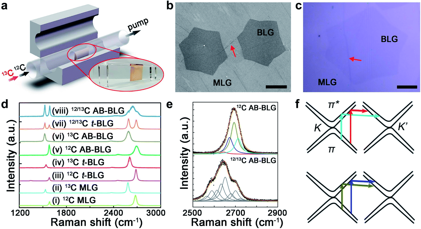 | ||
| Fig. 1 (a) Schematic of the experimental setup for synthesizing isotope-labeled graphene. Inset: a photograph of hung Cu foil on a quartz holder. (b and c) SEM image of graphene adlayers on Cu and OM images of graphene adlayer on a SiO2/Si substrate, respectively. The red arrows indicate the wrinkles formed in graphene. Scale bars: 20 μm. (d) Typical Raman spectra of MLG and BLG formed by 12C and 13C layer(s). (e) Peak fittings of the 2D peaks for 12C AB-BLG and 12/13C AB-BLG. (f) Double resonance Raman scattering paths that give rise to the four subpeaks in 2D peaks for AB-BLG. | ||
The stacking types of BLG can be rapidly identified by their Raman spectra, as shown in Fig. 1d. We note that for all the Raman maps in other figures, the region index and color are the same as those used here. For MLG and AB-BLG formed only by 12C atoms, their Raman G and 2D peaks both locate at ∼1580 cm−1 and ∼2680 cm−1, respectively, but for AB-BLG the intensity ratio between the 2D and G peaks (I2D/IG) is lower and the full-width-at-half-maximum of the 2D peak (FWHM2D) is larger.28 The Raman feature of t-BLG is similar to that of MLG but its 2D peak has a ∼10 cm−1 blueshift due to the reduction of the Fermi velocity.29 MLG, AB-BLG and t-BLG formed by 13C atoms exhibit the same spectral features as the 12C ones but all with significant peak redshifts of ∼60 cm−1 for the G peaks and ∼100 cm−1 for the 2D peaks.30 However, if the two layers in BLG are formed by different isotopes, although t-BLG still exhibits isolated G and 2D peaks, AB-BLG shows a much broader 2D peak that can be decomposed into eight Lorentzian lineshapes, instead of four Lorentzian lineshapes for AB-BLG formed by identical atoms (Fig. 1e).19Fig. 1f shows the double resonance scattering paths that give rise to the four Raman subpeaks in 12C (or 13C) AB-BLG. The colors of scattering paths are consistent with the subpeaks in Fig. 1e. The positions and widths of the decomposed 2D subpeaks are listed in Table S1.† All the Raman data of graphene are obtained after being transferred onto the SiO2/Si substrate. And different areas in the following distribution maps in Fig. 2–4 are divided based on their different Raman spectra, and the regulation of color related to the Raman spectra is the same as those shown in Fig. 1d, e.g. the 12C and 13C MLG are labeled in light green and light blue, respectively.
During the CVD process, CH4 precursors are dehydrogenated on the Cu surface at a high temperature, and in a general case, different graphene layers nucleate and start to grow simultaneously at the same sites of Cu structural defects, i.e., following the simultaneous growth mode (Mode I).18,19 Therefore, with sequentially introduced 12C and 13C precursors, as-grown MLG and its adlayers exhibit the same ring-like pattern that the core 12C graphene is surrounded by the 13C ring, which can be easily distinguished in the corresponding spectral maps from Raman spectroscopy. A schematic of the simultaneous growth mode is illustrated in Fig. 2a. Fig. 2b and c show the distribution maps of graphene with different isotopes, layer numbers and stacking types. In Fig. 2b, during the 12CH4 flow, regions (i) and (v) nucleate simultaneously, and the rapid expansion of (i) forms 12C MLG as the above layer, whereas the slow expansion of (v) forms the adlayer to it. Therefore, a core of 12C AB-BLG can be observed at the center of the domain. When the precursor is switched to 13CH4, the incoming 13C atoms attach to the 12C graphene edges to continue the growth, and the expanded 13C graphene region of the 12C adlayer retains the AB-stacking manner with the previously formed 12C MLG, to form the region (viii) for 12/13C AB-BLG. Fig. 2c shows another BLG stack formed by simultaneous growth but with half of it [(v) and (viii)] as AB-BLG and the other half [(iii) and (vii)] as t-BLG. The different stacking types are probably formed at the beginning of the nucleation stage. Later, each of the two halves expands from a 12C region to an in-plane 13C hetero-structural region. Nevertheless, Fig. 2b and c demonstrate that regardless of whether the BLG contains the same or different stacking types, the adlayers grown by this simultaneous mode all display the typical core-ring pattern in their scanning Raman maps.
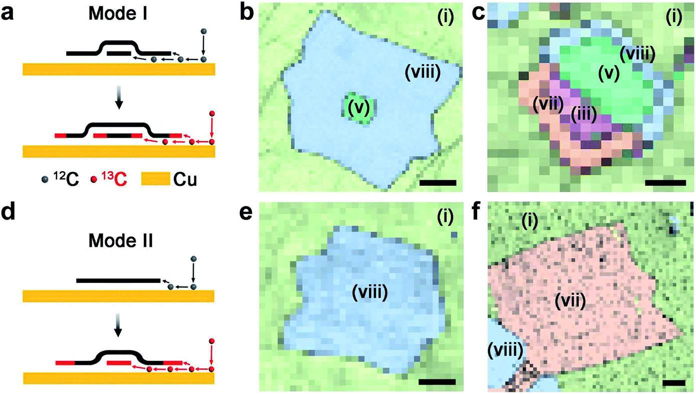 | ||
| Fig. 2 Schematic of the simultaneous growth mode (Mode I) for graphene adlayers (upper row) and the sequential growth mode (Mode II) for graphene adlayers (lower row). (a) Schematic of the simultaneous growth mode; (b and c) representative distribution maps of graphene adlayers grown from the simultaneous mode; (d) schematic of the sequential growth mode; (e and f) representative distribution maps of graphene adlayers grown from the sequential mode. Scale bars: 20 μm. | ||
Interestingly, some graphene adlayers do not follow the simultaneous mode to form multilayer stacks, but adopt a manner of the sequential growth mode (Mode II) that the adlayers grow at a much later stage than the top layer, as schematically shown in Fig. 2d. The adlayer here is drawn underneath the top layer as the simultaneous growth mode, and strict and critical proof is provided in Fig. S2† using surface functionalization experiments. Fig. 2e and f show the two distribution maps of graphene stacks and their corresponding Raman spectra. Different from the results in Fig. 2a–c that the adlayers are formed by both 12C and 13C atoms, in both maps for AB-BLG and t-BLG in Fig. 2d–f the adlayers contain only 13C atoms. Considering that in our experiments 13CH4 is introduced 1–2 hours later than 12CH4, the 12C-core-free pattern of these 13C adlayers actually demonstrates that they nucleate and grow sequentially at a very late stage after the nucleation and growth of the top layer. Moreover, both AB- and t-BLG are observed in this mode, indicating that this sequential growth is independent of the types for their interlayer vdW coupling with the top layer. Such sequential growth for graphene adlayers is similar to the results by Fang et al.19 and Hao et al.,20 but both of these previous results were obtained using a non-equilibrium growth environment by a Cu enclosure, in which the adlayers are formed on the external enclosure surface by diffused C through the Cu bulk from the interior enclosure surface. The precursor diffusivities inside and outside the enclosure differ by several orders of magnitude. However, the Cu substrate was vertically placed in the chamber with an equal distance of the front and back surfaces to the quartz tube in our experiments so that the CVD parameters for both Cu surfaces were identical (Fig. S3 and S4†). Under such equilibrium thermodynamics for the environment, graphene adlayers grown from the sequential mode were still frequently observed, on both surfaces of the hanging Cu substrates.
Fig. 3 shows another BLG with a more complicated Raman map pattern. An irregularly shaped BLG region [combined by (vi) and (viii)] is detected in the Raman map, which is actually composed of four different adlayer domains, as also can be seen from the OM image in Fig. S5.† The MLG background (the top layer) for these adlayers is formed by a hexagonal 12C core [partly shown by the combined region of (i) and (viii)] and its 13C expansion area [combined by (ii) and (vi)]. Moreover, a more careful inspection into these four BLG adlayers implies that they actually grow at different stages, owing to the fact that the ‘lower’ three adlayers in the map all have apparent nucleation 12C centers (as indicated by the red arrows). A schematic of the graphene growth process in this mapping area is displayed in Fig. 3b. With the 12CH4 source, 12C MLG [region (i)] grows on Cu first and the AB-BLG nuclei of domains 1, 2, and 3 [region (v),] also form at the same time, i.e., following the simultaneous growth mode (step A). When the C source is switched to 13CH4 (∼90 minutes later), 13C MLG [region (ii)] grows from the 12C MLG edge to form an in-plane isotope heterostructure (step B). During this process, the nuclei of 12C graphene adlayers also expand with the incoming 13C source, to form 12/13AB-BLG [region (viii)] when it is stacked with the 12C MLG in region (i), or form 13C AB-BLG [region (vi)] with the 13C MLG in region (ii). The nucleation of domain 4 adlayer occurs in step B and is apparently different from the nucleation of another three domain adlayers in step A. With an extended flow time of 13CH4 the four adlayers expand and coalesce into a continuous adlayer (step C). A series of control experiments and scanning Raman measurements were carried out to determine the proportion of graphene adlayers formed via simultaneous growth and sequential growth, as well as their corresponding layer stacking types. Here we have observed more than 120 graphene areas on 10 Cu samples from different batches and each with 2 cm × 2 cm area. The results are shown by pie charts in Fig. 3c. Approximately 63% of all the adlayers are formed via the simultaneous growth mode, and the rest of them (37%) are from the sequential growth mode. Moreover, for both modes the proportions of AB-stacked adlayers they form are close (83% for simultaneous growth and 81% for sequential growth), suggesting that the nucleation of the adlayers under the top layer by vdW interactions is independent of the growth modes.
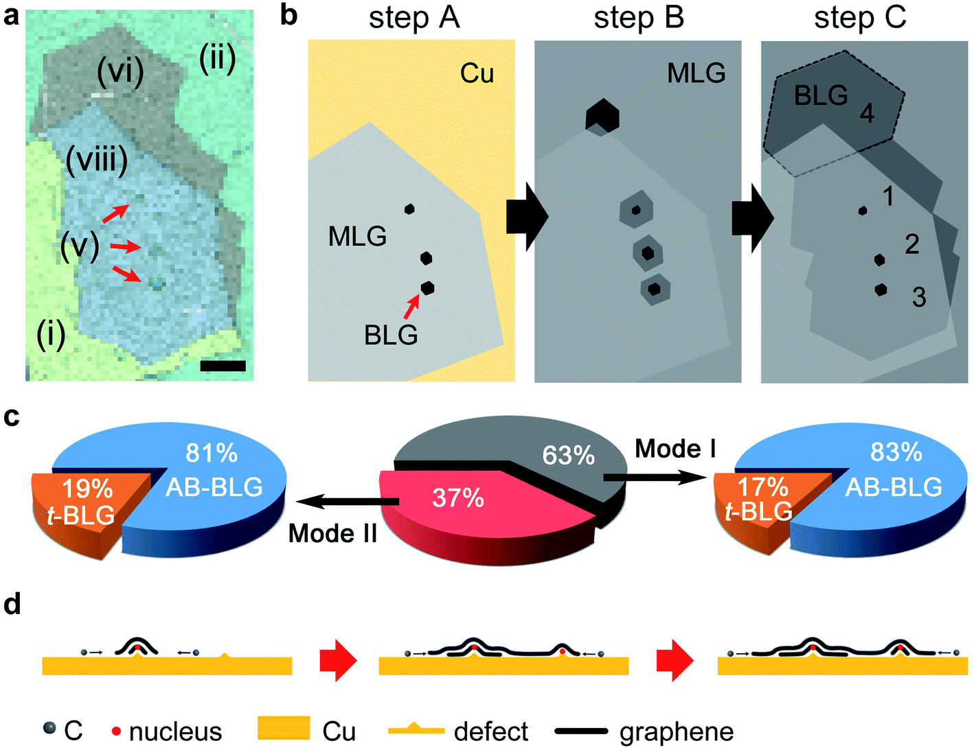 | ||
| Fig. 3 (a) The distribution map and (b) the growth process in each region for an AB-stacked graphene adlayer formed by four domains. (c) Pie charts for the proportions of different adlayer growth modes and their layer stacking types. (d) Schematic of the growth process for this graphene adlayer. Scale bar in (a): 50 μm. | ||
We propose the growth mechanism of graphene adlayers by sequential growth as follows. As mentioned recently by Luo et al.,14 when defective sites are covered by a graphene layer, the non-equilibrium C environment underneath this layer can result in the diffusion of sub-surface C atoms out of the bulk for the nucleation of graphene adlayers. These adlayer nuclei are considerably small (∼20–30 atoms) and it is not possible to observe them by Raman spectroscopy. The dehydrogenated C source from CH4 then diffuses to the nuclei for the simultaneous growth of all layers. This is true when the top graphene layer is small, and if considering the short diffusion paths of C atoms underneath the top layer before coalescence, only the center site has the largest chance to grow but the growth from other nuclei (formed when this site is covered) is eliminated. When the top layer is considerable larger, the growth of adlayers can be sequential, i.e., they grow after the moment the top layer expands to cover their nuclei. Because the coverage of the top layer is low, there is enough Cu surface for the dehydrogenation of CH4 to feed the growth of these sequential mode. A schematic for this proposed mechanism is illustrated in Fig. 3d.
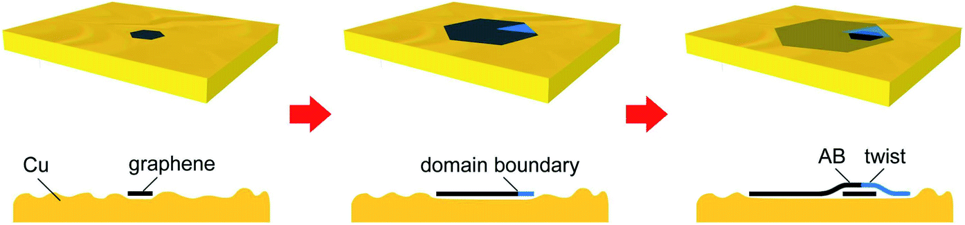
We further discuss the stacking orders of graphene adlayers by simultaneous and sequential growth modes, especially the sequentially grown ones, by combining scanning Raman maps with high-resolution AFM measurements. Raman signals from C-isotope-labeled graphene regions that are composed of MLG, AB-BLG and t-BLG are collected first. Using the Raman spectra in Fig. 1d, the isotopes and stacking orders of these graphene are revealed, as shown in Fig. 4a and c. The lower panels are the side views of the layered structures cutting at the red dashed lines in the maps, in which black denotes 12C graphene and red denotes 13C ones. Their corresponding OM images are shown in Fig. S6.† In Fig. 4a, the graphene includes a six-lobed star-like FLG stack and a hexagonal BLG stack next to it, both of which are decorated on a 12C MLG background of region (i). Because of the sequentially introduced isotopic CH4, the star-like FLG crystal exhibits a ring-like pattern alternated by 12C and 13C in all the layers, which is a fingerprint for the simultaneous growth mode of adlayers. Moreover, an AB-stacking was observed for all the layers in the regular ring-like lobes of this crystal, such as the 12C AB-BLG for region (v) and the 12/13C AB-BLG for region (viii). However, Raman information shows that one of the lobes of this crystal has different stacking orders with the others, for instance, as indicated by pink and orange colors for 12C t-BLG and 12/13C t-BLG, respectively. It suggests that for the two single-crystal-like layers of BLG in this crystal, there must be one layer that partly changes its lattice orientation during the growth. This is a surprising result because the graphene crystal expanded from a nucleus is always considered as a single crystal especially for a six-lobed one,31 and if we suppose that only MLG is nucleated and labeled by C isotopes, the lack of its stacking information with another layer actually suggests the incapability of the widely used ring-like C isotope Raman patterns in distinguishing the possible lattice misorientation of the crystal during its growth. For the hexagonal BLG crystal, it has a 12C core surrounded by a 13C ring, but the layer right above it does not show any hints of isotopic composition, indicating that the adlayer for this crystal is simultaneously grown. It is noteworthy that this crystal is also divided into AB- and t-BLG regions, and their boundary line is the extension from the misorientation boundary line in the star-like crystal, as indicated by the upper black dashed line. The modification of the stacking order in this hexagonal crystal suggests lattice misorientation in either the top or the bottom graphene “single crystal” layer.
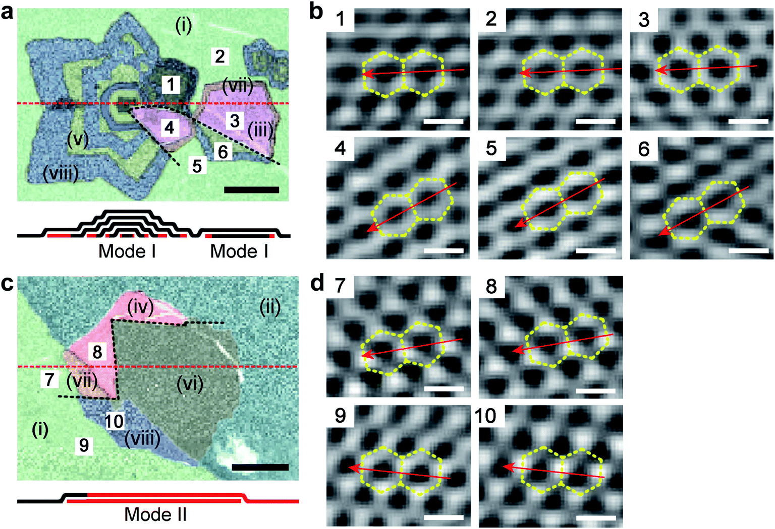 | ||
| Fig. 4 Isotope-labeled Raman maps of graphene adlayers and the corresponding Fourier transform images for the top graphene layers derived from atomic-resolution AFM. (a and c) The distribution maps of graphene with different isotopes, layer numbers and stacking types. The red dashed lines indicate the positions for the cross-view schematic of the stacks, and the black dashed lines indicate the positions of domain boundaries. The regions marked with Roman numerals are scanned by atomic-resolution AFM and their Fourier transform images are shown in (b and d). Scale bars in (a and c) are 25 μm, and in (b and d) are 0.25 nm. | ||
To reveal the lattice orientation of the top graphene layer in this map, we performed atomic-resolved AFM measurements and six regions in different crystals but at two sides of the boundary were scanned, as shown by the Fourier-transformed images in Fig. 4b. And the original AFM images corresponding to areas of two sides are shown in Fig. S7.† The measured hexagonal lattices with a lattice constant of ∼0.25 nm perfectly agree with the theoretical value of that of MLG (0.246 nm). For regions that are located at the same side of the boundary, i.e., regions (1–3) or regions (4–6), the same lattice orientation is observed regardless of the crystals, but for regions at different sides of the boundary, they exhibit apparently different lattice orientation. This result clearly demonstrates that the top layer crystal modifies its crystallinity from a single crystal to polycrystalline with two domain boundaries (black dashed lines). Because the cross of the two domain boundaries is very close to the nucleus site of the stack, it implies that lattice misorientation starts at the very beginning stage of crystal growth. It is worthy of note that moiré patterns are not observed in t-BLG regions, probably due to out-of-plane roughness resulting from the transfer process of graphene from Cu to a SiO2/Si substrate, so the crystallinity of the bottom layers cannot be determined, but we consider them as single crystals based on the low possibility that both bottom layer crystals modify their lattice orientation along the domain boundary of their shared top layer to ensure that only two types of stacking information appear in the Raman maps.32
Fig. 4c presents another example for the modification of the stacking order in a BLG stack. A hexagonal bottom layer crystal is located underneath the boundary line of the 12C of region (i) and 13C of region (ii) of the top layer, dividing the stack into the 12/13C BLG and 13C BLG regions. The bottom layer is entirely formed by 13C atoms, suggesting that it is grown from a sequential mode. However, as probed by Raman spectroscopy, the stacking order for the two layers are not the same for the whole stack, as indicated by the t- and AB-stacked regions separated by the black dashed line. Therefore, for the hexagonal BLG stack in this map, in total four different types of C composition and layer stacking are observed, i.e., 12/13C t-BLG [region (vii)], 13C t-BLG [region (iv)], 12/13C AB-BLG [region (viii)] and 13C AB-BLG [region (vi)]. To determine the location of the domain boundary (black dashed line), we performed atomic-resolved AFM measurements to the top graphene layer of this stack as well, for regions (7–10) at the two sides of the domain boundary. The different lattice orientation for regions (7 and 8) from regions (9 and 10) confirms that during the growth of the top layer crystal, it also changes from a single crystal to polycrystalline, so that the stacking order in the BLG is modified. It also needs to be noted from this map that the switching of isotopic CH4 during CVD does not change the lattice orientation of graphene during its growth.
The above atomic-level evidence demonstrates that, regardless of the growth of graphene adlayer from simultaneous or sequential modes, if modification of the layer stacking order is detected between it and its top layer, the corresponding lattice misorientation or domain boundary probably occurs in the top graphene layer of the stack, and its mechanism is proposed in Fig. 5. For graphene grow on polycrystalline Cu with different grain orientation and in-plane lattice constants, it is not a complete terrace or edge epitaxy process,33,34 and during the nucleation and expansion of a graphene layer on the Cu surface, the existence of Cu surface defects such as impurities and grain boundaries may lead to stress that allows the possibility of lattice misorientation occurrence in graphene.31 If the formation energy of the in-plane graphene single-crystal lattice is higher than the energy it needs to consume to overcome the barrier at these Cu defects, graphene will be forced to change its lattice orientation and form in-plane defects to continue the growth. However, the Cu substrate underneath the graphene also experiences some level of surface reconstruction induced by the covered graphene, for instance, a possibly atomic-level flatter surface smoothened by pre-melting Cu.35 This reconstructed Cu surface provides a lower energy barrier to overcome for the later-arrived bottom layer graphene edges. Moreover, the limited space between the top graphene layer and Cu lowers the freedoms of formed bottom graphene, making it prefer to slightly rotate itself on the pre-melting Cu for the release of thermal stress rather than generate an in-plane line defect.31 Therefore, after paving the way on the Cu surface by the top layer, the bottom graphene tends to maintain its crystallinity and form a single crystal below the top polycrystalline layer, and a domain boundary that separates the BLG into different stacking orders appears. It needs to be noticed that in Fig. 5 the graphene adlayer is illustrated as sequentially grown, but our proposed mechanism also includes the simultaneously grown adlayers.
 | ||
| Fig. 5 Schematic illustration of the mechanism for the modification of the layer stacking order in a graphene stack during its growth. | ||
3. Conclusions
In conclusion, we investigate the CVD growth of graphene adlayers on Cu using C isotope labeling, Raman spectroscopy, and high-resolution AFM. The results show that the growth of graphene adlayers follows both simultaneous and sequential modes with their top layer, regardless of the CVD environment for both Cu surfaces being in equilibrium or not. The sequentially grown graphene adlayers account for approximately 37% of all the adlayers, but the proportions of AB- and t-BLG these two modes form are approximately the same. Moreover, to investigate the domain boundary in a BLG stack, i.e., the boundary that separates AB- and t-BLG, we perform atomic-resolution AFM to reveal the lattice orientation of the top layer crystals in such stacks, and find that although these crystals exhibit a single-crystal-like shape and ring-like Raman patterns from isotopes, they are actually polycrystalline graphene. Based on experimental evidence we propose the growth mechanism of these BLG domain boundaries as that the expansion of the firstly-grown graphene top layers on the Cu surface helps pave the way for growing bottom layer graphene into single crystals.4. Methods
Synthesis of isotope-labeled graphene stacks
Low-pressure CVD was adopted for graphene growth.20 Cleaned Cu foil (#46365, Alfa Aesar China Chemical Co., Ltd.) was loaded vertically using a quartz holder at the center of the chamber and heated to 1060 °C under 300 standard cubic centimeter per minute (sccm) H2. The Cu foil was then oxidized for 10 minutes with 1 sccm O2, followed by introducing a mixed gas of 200–300 sccm H2 and 0.2–0.3 sccm 12CH4 and then 13CH4 for growth. Finally, the chamber was naturally cooled down to room temperature. The temperature and gas flow program in the CVD process are shown in Fig. S1.†After growth, graphene on Cu was transferred to silicon substrates with 300 nm-thick oxide layers by a conventional poly(methyl methacrylate) (PMMA, AR-P 679.04, GermanTech Co., Ltd.)-assisted method.10 After the removal of PMMA using dichloromethane (CH2Cl2), the sample was rinsed in isopropanol (IPA) and dried using a nitrogen gun.
Characterization
Characterization of graphene was carried out by SEM (5 kV, S-3400 I, Hitachi Co., Ltd.), OM (un-polarized white light, Olympus BXFM-ILHS, Olympus Co., Ltd.), and confocal micro-Raman spectroscopy (532 nm wavelength excitation laser, LabRAM HR Evolution, Horiba Co., Ltd.); all the Raman spectra and distribution maps were analyzed using LabSpec 6 software. And high-resolution AFM (Asylum Research, model: Cypher) was performed.Author contributions
All authors have given approval to the final version of the manuscript.Conflicts of interest
The authors declare no competing financial interest.Acknowledgements
This work was financially supported by the National Key Scientific Instruments and Equipment Development Project of China (61427901) and the National Science Foundation of China (11872330).References
- A. K. Geim and K. S. Novoselov, The rise of graphene, Nat. Mater., 2007, 6, 183–191 CrossRef CAS.
- K. S. Novoselov, A. K. Geim, S. V. Morozov, D. Jiang, Y. Zhang, S. V. Dubonos, I. V. Grigorieva and A. A. Firsov, Electric field effect in atomically thin carbon films, Science, 2004, 306, 666–669 CrossRef CAS.
- K. S. Novoselov, V. I. Fal'ko, L. Colombo, P. R. Gellert, M. G. Schwab and K. Kim, A roadmap for graphene, Nature, 2012, 490, 192–200 CrossRef CAS.
- A. H. Castro Neto, F. Guinea, N. M. R. Peres, K. S. Novoselov and A. K. Geim, The electronic properties of graphene, Rev. Mod. Phys., 2009, 81, 109–162 CrossRef CAS.
- A. W. Tsen, L. Brown, M. P. Levendorf, F. Ghahari, P. Y. Huang, R. W. Havener, C. S. Ruiz-Vargas, D. A. Muller, P. Kim and J. Park, Tailoring electrical transport across grain boundaries in polycrystalline graphene, Science, 2012, 336, 1143–1146 CrossRef CAS.
- A. W. Tsen, L. Brown, R. W. Havener and J. Park, Polycrystallinity and stacking in CVD graphene, Acc. Chem. Res., 2013, 46, 2286–2296 CrossRef CAS.
- Y. Zhang, T. T. Tang, C. Girit, Z. Hao, M. C. Martin, A. Zettl, M. F. Crommie, Y. Ron Shen and F. Wang, Direct observation of a widely tunable bandgap in bilayer graphene, Nature, 2009, 459, 820–823 CrossRef CAS.
- Y. Cao, V. Fatemi, S. Fang, K. Watanabe, T. Taniguchi, E. Kaxiras and P. Jarillo-Herrero, Unconventional superconductivity in magic-angle graphene superlattices, Nature, 2018, 556, 43–50 CrossRef CAS.
- Y. Cao, V. Fatemi, A. Demir, S. Fang, S. L. Tomarken, J. Y. Luo, J. D. Sanchez-Yamagishi, K. Watanabe, T. Taniguchi, E. Kaxiras, R. C. Ashoori and P. Jarillo-Herrero, Correlated insulator behaviour at half-filling in magic-angle graphene superlattices, Nature, 2018, 556, 80–84 CrossRef CAS.
- X. Li, W. Cai, J. An, S. Kim, J. Nah, D. Yang, R. Piner, A. Velamakanni, I. Jung, E. Tutuc, S. K. Banerjee, L. Colombo and R. S. Ruoff, Large-area synthesis of high-quality and uniform graphene films on copper foils, Science, 2009, 324, 1312–1314 CrossRef CAS.
- S. Bae, H. Kim, Y. Lee, X. Xu, J. S. Park, Y. Zheng, J. Balakrishnan, T. Lei, H. R. Kim, Y. I. Song, Y. J. Kim, K. S. Kim, B. Ozyilmaz, J. H. Ahn, B. H. Hong and S. Iijima, Roll-to-roll production of 30-inch graphene films for transparent electrodes, Nat. Nanotechnol., 2010, 5, 574–578 CrossRef CAS.
- L. Gao, W. Ren, H. Xu, L. Jin, Z. Wang, T. Ma, L. P. Ma, Z. Zhang, Q. Fu, L. M. Peng, X. Bao and H. M. Cheng, Repeated growth and bubbling transfer of graphene with millimetre-size single-crystal grains using platinum, Nat. Commun., 2012, 3, 699 CrossRef.
- Y. Hao, M. S. Bharathi, L. Wang, Y. Liu, H. Chen, S. Nie, X. Wang, H. Chou, C. Tan, B. Fallahazad, H. Ramanarayan, C. W. Magnuson, E. Tutuc, B. I. Yakobson, K. F. McCarty, Y. W. Zhang, P. Kim, J. Hone, L. Colombo and R. S. Ruoff, The role of surface oxygen in the growth of large single-crystal graphene on copper, Science, 2013, 342, 720–723 CrossRef CAS.
- D. Luo, M. Wang, Y. Li, C. Kim, K. M. Yu, Y. Kim, H. Han, M. Biswal, M. Huang, Y. Kwon, M. Goo, D. C. Camacho-Mojica, H. Shi, W. J. Yoo, M. S. Altman, H. J. Shin and R. S. Ruoff, Adlayer-free large-area single crystal graphene grown on a Cu(111) foil, Adv. Mater., 2019, 31, 1903615 CrossRef.
- S. Nie, W. Wu, S. Xing, Q. Yu, J. Bao, S.-S. Pei and K. F. McCarty, Growth from below: bilayer graphene on copper by chemical vapor deposition, New J. Phys., 2012, 14, 093028 CrossRef.
- X. Zhang, L. Wang, J. Xin, B. I. Yakobson and F. Ding, Role of hydrogen in graphene chemical vapor deposition growth on a copper surface, J. Am. Chem. Soc., 2014, 136, 3040–3047 CrossRef CAS.
- P. Wu, X. Zhai, Z. Li and J. Yang, Bilayer graphene growth via a penetration mechanism, J. Phys. Chem. C, 2014, 118, 6201–6206 CrossRef CAS.
- Q. Li, H. Chou, J. H. Zhong, J. Y. Liu, A. Dolocan, J. Zhang, Y. Zhou, R. S. Ruoff, S. Chen and W. Cai, Growth of adlayer graphene on Cu studied by carbon isotope labeling, Nano Lett., 2013, 13, 486–490 CrossRef CAS.
- W. Fang, A. L. Hsu, R. Caudillo, Y. Song, A. G. Birdwell, E. Zakar, M. Kalbac, M. Dubey, T. Palacios, M. S. Dresselhaus, P. T. Araujo and J. Kong, Rapid identification of stacking orientation in isotopically labeled chemical-vapor grown bilayer graphene by Raman spectroscopy, Nano Lett., 2013, 13, 1541–1548 CrossRef CAS.
- Y. Hao, L. Wang, Y. Liu, H. Chen, X. Wang, C. Tan, S. Nie, J. W. Suk, T. Jiang, T. Liang, J. Xiao, W. Ye, C. R. Dean, B. I. Yakobson, K. F. McCarty, P. Kim, J. Hone, L. Colombo and R. S. Ruoff, Oxygen-activated growth and bandgap tunability of large single-crystal bilayer graphene, Nat. Nanotechnol., 2016, 11, 426–431 CrossRef CAS.
- L. Brown, R. Hovden, P. Huang, M. Wojcik, D. A. Muller and J. Park, Twinning and twisting of tri- and bilayer graphene, Nano Lett., 2012, 12, 1609–1615 CrossRef CAS.
- R. W. Havener, H. Zhuang, L. Brown, R. G. Hennig and J. Park, Angle-resolved Raman imaging of interlayer rotations and interactions in twisted bilayer graphene, Nano Lett., 2012, 12, 3162–3167 CrossRef CAS.
- K. Kim, S. Coh, L. Z. Tan, W. Regan, J. M. Yuk, E. Chatterjee, M. F. Crommie, M. L. Cohen, S. G. Louie and A. Zettl, Raman spectroscopy study of rotated double-layer graphene: misorientation-angle dependence of electronic structure, Phys. Rev. Lett., 2012, 108, 246103 CrossRef.
- M. Hadi Khaksaran and I. I. Kaya, Spontaneous nucleation and growth of graphene flakes on copper foil in the absence of external carbon precursor in chemical vapor deposition, ACS Omega, 2018, 3, 12575–12583 CrossRef.
- J. Kraus, M. Böbel and S. Günther, Suppressing graphene nucleation during CVD on polycrystalline Cu by controlling the carbon content of the support foils, Carbon, 2016, 96, 153–165 CrossRef CAS.
- B. Deng, Z. Pang, S. Chen, X. Li, C. Meng, J. Li, M. Liu, J. Wu, Y. Qi, W. Dang, H. Yang, Y. Zhang, J. Zhang, N. Kang, H. Xu, Q. Fu, X. Qiu, P. Gao, Y. Wei, Z. Liu and H. Peng, Wrinkle-free single-crystal graphene wafer grown on strain-engineered substrates, ACS Nano, 2017, 11, 12337–12345 CrossRef CAS.
- N. Liu, L. Fu, B. Dai, K. Yan, X. Liu, R. Zhao, Y. Zhang and Z. Liu, Universal segregation growth approach to wafer-size graphene from non-noble metals, Nano Lett., 2011, 11, 297–303 CrossRef CAS.
- A. C. Ferrari, J. C. Meyer, V. Scardaci, C. Casiraghi, M. Lazzeri, F. Mauri, S. Piscanec, D. Jiang, K. S. Novoselov, S. Roth and A. K. Geim, Raman spectrum of graphene and graphene layers, Phys. Rev. Lett., 2006, 97, 187401 CrossRef CAS.
- Z. Ni, Y. Wang, T. Yu, Y. You and Z. Shen, Reduction of Fermi velocity in folded graphene observed by resonance Raman spectroscopy, Phys. Rev. B: Condens. Matter Mater. Phys., 2008, 77, 235403 CrossRef.
- X. Li, W. Cai, L. Colombo and R. S. Ruoff, Evolution of graphene growth on Ni and Cu by carbon isotope labeling, Nano Lett., 2009, 9, 4268–4272 CrossRef CAS.
- Y. Wu, Y. Hao, H. Y. Jeong, Z. Lee, S. Chen, W. Jiang, Q. Wu, R. D. Piner, J. Kang and R. S. Ruoff, Crystal structure evolution of individual graphene islands during CVD growth on copper foil, Adv. Mater., 2013, 25, 6744–6751 CrossRef CAS.
- J. B. Wu, X. Zhang, M. Ijas, W. P. Han, X. F. Qiao, X. L. Li, D. S. Jiang, A. C. Ferrari and P. H. Tan, Resonant Raman spectroscopy of twisted multilayer graphene, Nat. Commun., 2014, 5, 5309 CrossRef CAS.
- X. Zhang, Z. Xu, L. Hui, J. Xin and F. Ding, How the orientation of graphene is determined during chemical vapor deposition growth, J. Phys. Chem. Lett., 2012, 3, 2822–2827 CrossRef CAS.
- J. Dong, L. Zhang, K. Zhang and F. Ding, How graphene crosses a grain boundary on the catalyst surface during chemical vapour deposition growth, Nanoscale, 2018, 10, 6878–6883 RSC.
- Z.-J. Wang, G. Weinberg, Q. Zhang, T. Lunkenbein, A. Klein-Hoffmann, M. Kurnatowska, M. Plodinec, Q. Li, L. Chi, R. Schloegl and M.-G. Willinger, Direct observation of graphene growth and associated copper substrate dynamics by in situ scanning electron microscopy, ACS Nano, 2015, 9, 1506–1519 CrossRef CAS.
Footnote |
| † Electronic supplementary information (ESI) available: Details on surface aryl functionalization of graphene stacks, the CVD growth process, peak positions and widths of the decomposed 2D subpeaks, the vertically placed Cu substrate, and OM and AFM images of graphene adlayers. See DOI: 10.1039/d0na00982b |
| This journal is © The Royal Society of Chemistry 2021 |