
 Open Access Article
 This Open Access Article is licensed under a Creative Commons Attribution-Non Commercial 3.0 Unported Licence
Optical visualization and imaging of nanomaterials
Xiaofei
Shi†
,
Siming
Zhao†
,
Fei
Wang†
,
Qinyuan
Jiang†
,
Chenhao
Zhan
,
Run
Li
and
Rufan
Zhang
 *
*
Beijing Key Laboratory of Green Chemical Reaction Engineering and Technology, Department of Chemical Engineering, Tsinghua University, Beijing 100084, China. E-mail: zhangrufan@tsinghua.edu.cn
First published on 22nd December 2020
Abstract
Direct visualization and imaging of nanomaterials under ambient conditions is of great significance for their characterization and application. In most cases, the observation of individual nanomaterials usually requires high-resolution electron microscopes under high vacuum. In comparison, an optical microscope is much more convenient due to its facile operation and open space. However, the resolution of optical microscopes is much lower than that of electron microscope-based tools. Therefore, effective visualization and imaging strategies for nanomaterials are required to realize their direct observation, accurate location and controllable manipulation. In this review, we summarized the progress of optical visualization and imaging strategies for nanomaterials in recent years, including vapor-condensation-assisted optical visualization, nanoparticle-assisted optical visualization, substrate-assisted optical visualization and fluorescence visualization, and the applications of these techniques were also introduced. We believe that this review will inspire further improvement in optical visualization of nanomaterials and drive the application of nanomaterials in a broader domain.
1 Introduction
Nanomaterials have been studied extensively in the past few decades owing to their unique mechanical, thermal, electrical and optical properties.1,2 Fast and facile location and observation of samples is generally considered the first step in a series of characterization studies such as on the structures, properties and applications of these nanomaterials. Notably, in situ observation of dynamic processes occurring on nanomaterials (e.g. reactions and phase changes) has drawn much attention because it provides more information for revealing mechanisms. Unfortunately, commonly used observation tools for visualizing nanomaterials based on electron microscopes require high vacuum conditions, which significantly limits the in situ observation. Even advanced environmental electron microscopes are still very difficult to operate under real conditions. Moreover, in situ manipulation of nanomaterials is severely restricted by their tiny chambers. Hence, a facile visualization tool that can be operated under ambient or any specific conditions is urgently needed for the further development of nanoscience.Optical visualization is a conventional yet effective way to obtain morphological information of materials. With the assistance of optical visualization, real-time and true-color images can be collected in situ in an almost non-destructive way, which has many advantages in observing dynamic processes. Besides, compared with electron microscopes and scanning probe microscopes, visualization with optical microscopes has advantages of low cost, simplicity and mild operation conditions. However, optical visualization of nanomaterials faces many challenges due to the low resolution and large beam sizes of optical microscopes, which set limits on its application in the imaging of nanomaterials. As is known, the sizes of many nanomaterials are much less than the limit of optical resolution (ca. 200 nm). For example, it is impossible to directly visualize single carbon nanotubes (CNTs) using a common optical microscope because the illumination beam size is several orders of magnitude larger than the diameters of CNTs (usually 1–20 nm).3 Therefore, effective visualization and imaging strategies for nanomaterials should be rationally designed to realize their direct observation, accurate location, controllable manipulation, performance characterization and subsequent utilization. During the past few years, various strategies were proposed for optically visualizing and imaging nanomaterials. For example, by depositing visible “labels” or utilizing certain optical phenomena, researchers have made great progress in optically visualizing various nanomaterials, such as CNTs, graphene and nanofibers, thus paving the way for subsequent research on their properties and applications. Moreover, by elaborately designing and modifying setups, researchers can in situ observe chemical reactions or directly manipulate nanomaterials, which will further expand the application of optical microscopy and provide more insights into the mechanisms of dynamic processes at the microscale or even the nanoscale.
In this review, we summarize the optical visualization and imaging strategies of nanomaterials, including nanoparticle-assisted visualization, substrate-assisted visualization and fluorescence visualization. Besides, applications of these techniques in the imaging of CNTs and other nanomaterials are also briefly discussed, followed by an introduction of state-of-the-art methods for modifying optical microscopes. Finally, we provide our perspectives on the development directions of this field in the future.
2. Marker-assisted optical visualization
2.1 Vapor-condensation-assisted optical visualization
Vapor condensation is a ubiquitous phenomenon in nature and daily life, e.g., the formation of dewdrops, water recycling in meteorology, water harvesting, defrosting, etc.4–6 Typically, when a flow of warm or supersaturated water vapor is blown onto a sample, it will condense on some nuclei attached to the sample and form nanosized water droplets which then gradually grow bigger and bigger. The droplets can scatter light and thus become highly visible with the naked eye. This phenomenon can be employed to visualize nanomaterials and exhibits many advantages compared with other methods. For example, vapor can quickly condense into droplets on nanomaterials and the condensed water will also evaporate spontaneously in a few seconds, leaving samples as clean as before.7–10 Apparently, this vapor-condensation-assisted (VCA) optical visualization is very efficient and of low cost. Moreover, it is a non-destructive method that does not induce any impurities on the samples, keeping them intact for further characterization and application. Besides, this method can also be conveniently integrated with other facilities, such as a Raman spectroscope, fluorescence microscope, probe console, etc. The VCA method can effectively make a variety of nanostructures visible under ambient conditions. In this section, we discuss the application of the VCA visualization method for various nanomaterials such as CNTs, graphene, nanofibers, nanofilms, etc.In 2014, the Jiang group first reported the observation of ultralong CNTs on a silicon substrate assisted by water vapor condensation under an optical microscope.11 When blowing a flow of warm vapor onto a silicon substrate carrying horizontally aligned CNTs, numerous tiny droplets immediately formed on these CNTs, which can thus be clearly observed under an optical microscope (Fig. 1a and b). It should be noted that the VCA images did not show real CNTs but their outlines which were made up of water droplets attached to them (Fig. 1c–g). It should also be noted that the image would spontaneously disappear in a few seconds when blowing was stopped. Fortunately, this imaging process was reversible and could be simply repeated many times. Later, researchers found that the imaging process could be prolonged simply by freezing the tiny water droplets into ice with the assistance of liquid nitrogen. Besides, it was also reported that the vapor condensation was nucleated on the surface impurities of CNTs, which was evidenced by the disappearance of the VCA image after annealing the CNTs in a hydrogen atmosphere at 700 °C to remove amorphous carbon. Meanwhile, it was observed that the VCA visualization also worked well for clean CNTs after hydrogen annealing and subsequent argon plasma treatment, with the proposed mechanism of substrate hydrophilization. In addition, they also achieved VCA visualization of a thin layer (no more than 1 nm thick) of deposited amorphous carbon and Fe, respectively, which could hardly be observed using conventional optical microscopes (Fig. 1h and i). Generally, there are also other vapors suitable for VCA imaging, as long as they are easy to condense and evaporate, and are more likely to condense either onto the nanostructure or the substrate to form a contrast between the nanostructure and the substrate. Later in 2016, the Jiang group proposed a similar approach to visualize ultralong CNTs on the silicon substrate using glucose spray as vapor.12 However, unlike the case of water vapor, the condensation of glucose vapor was realized via Coulomb interaction between the as-grown CNTs and glucose spray which were both negatively charged.
 | ||
| Fig. 1 (a) A schematic diagram of the experimental setup for the VCA visualization of CNTs. (b) Screenshots of a streaming video. (c) A VCA image and (d) the corresponding SEM image of ultralong CNTs. Scale bars: 200 μm. (e) A higher-magnification VCA image of CNTs. Scale bar: 100 μm. (f, g) Schematic diagrams showing the nucleation and microdroplet formation process. (h, i) VCA images of patterns for 1 nm amorphous carbon and 0.2 nm Fe, respectively. Scale bars: 500 μm. (j) Illustration of the experimental setup for visualizing the capture process of aerosols on nanofibers. Images of the in situ capture of (k) wetting droplets, (l) nonwetting droplets, and (m) solid particles by the nanofibers. (n) An illustration showing the formation of the core–shell structure by depositing ice around the CNTs. (o, p) Optical images of graphene grown on Cu (o) before and (p) after condensing water vapor. (q) Schematic diagram showing the mechanism of distinguishing between monolayer and multilayer graphene. The scale bar of the embedded figure is 20 μm, and those of the others are 200 μm. | ||
Motivated by the VCA visualization, a modified prototype based on individual suspended ultralong CNTs was developed by coating ice onto a nanotube in a cryogenic air environment.13 The ice–CNT hybrid with a core–shell structure was formed by freezing the supercooled water vapor onto suspended CNTs on a programmable cryogenic platform (Fig. 1n). A remarkable advance over the VCA imaging above is that this method can maintain visibility as long as the temperature is sufficiently low to ensure a supercooling water vapor environment, allowing more complicated characterization and investigation of the CNTs.
With a similar mechanism to VCA visualization of CNTs, Zhang et al. investigated the capture and evolution process of different aerosols on polyimide nanofibers under an optical microscope.14 It was found that the distinct capture and evolution behaviors of different types of aerosols, including wetting and non-wetting droplets, were due to their different wetting properties, such as specific energy, viscosity, fluidity, etc., which provide new insights for understanding the nanoscale filtration mechanism (Fig. 1j–m).
In addition to one-dimensional nanomaterials such as CNTs and nanofibers, VCA visualization is also feasible for nanosized 2-D graphene (Fig. 1o and p).15,16 Due to the unique wetting properties of graphene, graphene-covered and uncovered surfaces show different wetting behaviors, which lead to a difference in the distribution and morphology of microscopic water droplets, resulting in distinct color contrast and enabling the observation of graphene domains. This approach is applicable for a wide variety of substrates, including copper, plasma-treated PET, pristine silicon, silicon oxide, quartz, glass, etc. Besides, this method can also be used to facilely distinguish monolayer and multilayer graphene since the wetting properties of the graphene-covered surface are sensitive to the number of graphene layers (Fig. 1q). Similarly, Duong et al. observed the grain boundaries of large-area graphene (grown on copper foil) directly without transfer of the graphene by optical microscopy, and the influence of graphene grain boundaries on crack propagation and termination was clearly visualized.16 This imaging technique was realized by selectively oxidizing the underlying copper foil through graphene grain boundaries functionalized with O and OH radicals generated by ultraviolet irradiation under moisture-rich ambient conditions. This approach can be used as a simple protocol for evaluating the grain boundaries of other two-dimensional layered structures, such as boron nitride and exfoliated clays.
It is seen that the VCA visualization provides a simple and efficient tool for optical observation and characterization of various nanostructures at the macroscale. However, the vapor condensation mechanisms, especially for ultralong CNTs, are still ambiguous and require further investigation.
2.2 Nanoparticle-assisted optical visualization
As is known, when the diameter of tiny particles such as smoke, dust, small water droplets, aerosols, etc., is equal to or just slightly larger than the wavelength of light, Mie scattering occurs which results in stronger light in the forward direction than in the backward direction.17,18 This phenomenon plays a key role in the optical visualization of nanomaterials assisted by decoration with nanoparticles with diameters in the range of visible light and has enabled a series of novel approaches to achieve the facile optical observation and characterization of different nanomaterials. In this section, we discuss the applications of nanoparticle-assisted optical visualization of nanomaterials, including CNTs, graphene and nanofibers.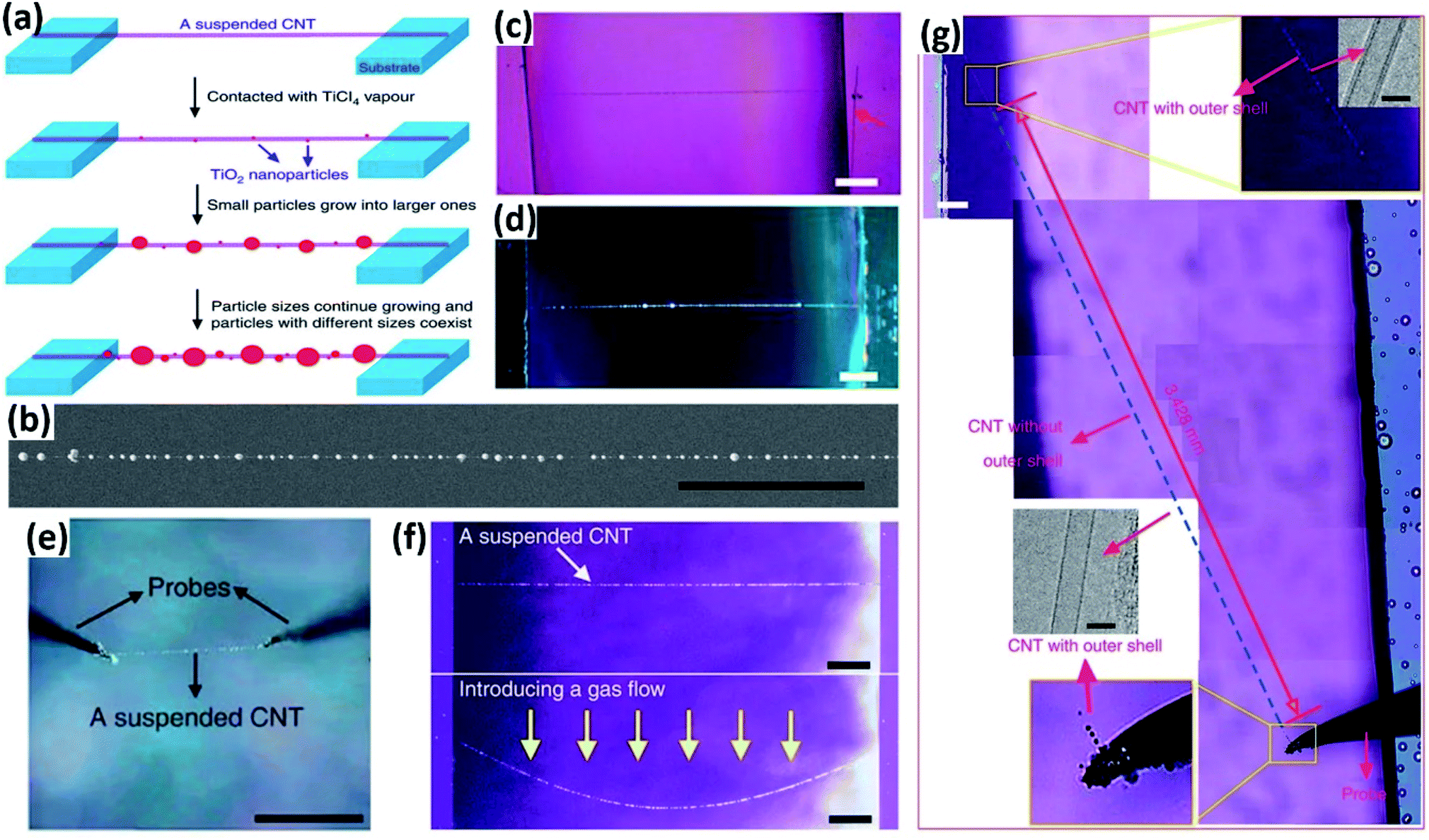 | ||
| Fig. 2 (a) Schematic illustration for depositing TiO2 nanoparticles on suspended CNTs. (b) SEM images of suspended CNTs decorated with TiO2 nanoparticles prepared with a contact time of 5.0 s. Scale bar, 10 μm. (c) Bright field mode and (d) dark field mode images of CNTs with small TiO2 nanoparticles. Scale bar, 100 μm. (e) Cutting a CNT segment from a suspended CNT using two probes. Scale bar, 50 μm. (f) A suspended CNT and gas-flow-induced bending of the CNT. Scale bar, 100 μm. (g) A 3.43 mm-long single-walled CNT being pulled out from the DWCNT. Scale bar, 20 μm; 2 nm (lower inset); 2 nm (upper inset). | ||
MoS2 was reported as another type of nanoparticle which can decorate CNTs for their optical visualization. Besides, the combination of CNTs and MoS2 nanoparticles along with their strong coupling also facilitates the fabrication of CNT–MoS2-based functional materials. The CNTs–MoS2 hybrids are usually synthesized through an in situ CVD process to guarantee clean interfaces between CNTs and MoS2 nanoparticles (Fig. 3a).23 The MoS2 nanoparticles are attached to CNTs in the form of an ultrathin layer, which helps image the horizontally aligned CNTs as white lines on a nearly transparent quartz substrate under an optical microscope, with a similar scattering mechanism as the aforementioned TiO2 nanoparticles (Fig. 3b and c). Notably, MoS2 nanoparticles can easily visualize CNTs on substrates, while TiO2 and SnO2 nanoparticles can only visualize suspended CNTs. It is also found that the CNTs–MoS2 hybrids inherited both the electrical transport properties from MoS2 films and the unique optoelectronic properties of CNTs.
 | ||
| Fig. 3 (a) Illustration of the furnace setup for CNTs–MoS2 hybrid synthesis. (b) Optical and (c) SEM images of CNTs–MoS2 hybrids on quartz substrates. (d) Schematic illustration of the designed sequential CVD procedure for growing MoS2 on CNTs. (e) SEM image of MoS2 triangular domains nucleating on an individual CNT. (f) Optical image for a longer MoS2 growth time. (g) Optical image of the graphene–MoS2 heterostructure. | ||
Liu et al. also demonstrated a strongly coupled 1D CNT and 2D MoS2 monolayer hybrid structure through a controlled sequential CVD process and found that the CNTs can be clearly observed due to the enhanced contrast of multi-layered MoS2 along the CNTs under an optical microscope.24 It was found that the post hydrogen annealing before MoS2 growth is a key factor for creating a clean interface between CNTs and MoS2, and the climbing-up growth behavior of MoS2 over the CNTs ensures a large interaction area at the interface, which together lead to strong interfacial coupling both mechanically and electronically (Fig. 3d–f).
Additionally, MoS2 also facilitates the optical visualization of graphene sheets on silica.25 MoS2 single layers were formed through seeded CVD growth with the dangling bonds and lithographic residues at the edge of graphene as crystal nucleation sites, rendering the graphene outline as brighter regions under an optical microscope (Fig. 3g).
The fundamental studies above showed that MoS2 particles not only act as an important functional component in the hybrids, but also assisted with the visible observation of the hybrid materials under an optical microscope, which offers a new way to develop novel hybridized materials and their facile optical characterization.
 | ||
| Fig. 4 Optical microscope images of individual suspended CNTs decorated with (a) (NH4)2SO4 nanoparticles, (b) NH4NO3 nanoparticles, (c) ferrocene, (d) paraffin wax, (e) dodecanoic acid and (f) abietic acid. (g) SEM image of Ag NWs on a SiO2/Si substrate. (h) Optical bright-field mode image and (i) dark-field mode image of Ag NWs decorated with sulfur nanoparticles corresponding to (g). Scale bar, 20 μm in (a–c, e–i) and 50 μm in (d). (j, k) Removal of sulfur nanoparticles from CNTs. Optical microscope images of partially suspended CNTs and supported CNTs decorated with sulfur nanoparticles at 120 °C for (j) 5 min and (k) after being heated at 120 °C for 1 min. Scale bar, 100 μm. | ||
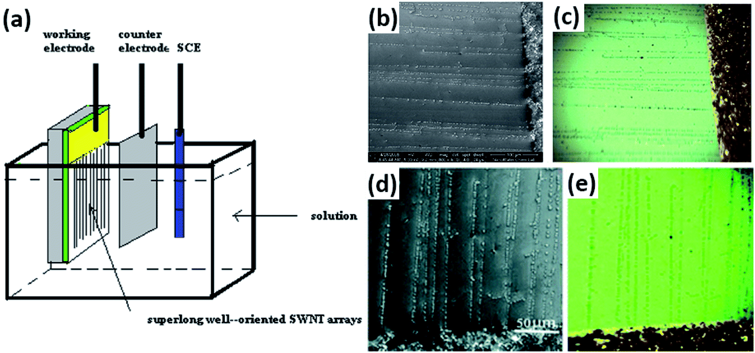 | ||
| Fig. 5 (a) Schematic illustration of the electrodeposition of Ag nanoparticles on SWNT arrays. (b, c) SEM image and optical photo taken from the same area of long oriented SWNT arrays after electrodeposition, respectively. (d, e) SEM image and optical photo taken from the same area of long-oriented SWNT arrays after electrodeposition, respectively. | ||
Au and Pd nanoparticles were also employed for deposition onto CNTs for visualization. Chu et al. reported the seeded growth of Au and Pd nanoparticles on the surfaces of CNTs on silicon substrates using a tandem electroless technique with high selectivity (Fig. 6a–f).29,30 It was found that the visibility of the Au or Pd nanoparticle-deposited CNTs benefited from the coupled surface plasmon resonance adsorption of adjacent Au nanoparticles with small gaps, which thus remarkably facilitated both the Raman characterization and the device fabrication of individual CNTs under optical microscopes. Moreover, this electroless method requires no selectivity on types, defects, or conductivity of CNTs, which thus ensures the uniform decoration of all CNTs.
 | ||
| Fig. 6 (a) Scheme of the controlled decoration of gold nanoparticles on CNTs based on gold seeds via (i) gold seed decoration and (ii) subsequent seeded growth stages. (b) Scheme of the controlled decoration of gold nanoparticles on SWNTs based on palladium seeds via (i) PdCl2 adsorption, (ii) H2 reduction, and (iii) seeded growth stages. (c) SEM image and (d) optical image of 10 CNTs grown on SiOx/Si after gold decoration. (e) Optical image and (f) the corresponding SEM image of the gold nanoparticle-decorated SWNT arrays on SiOx/Si. (g) Chemical structure of pNBA (top) and schematic illustration of the monoclinic unit cell of pNBA powder as extracted from X-ray diffraction analysis (bottom). (h) Dark field optical microscopy images of pNBA nanocrystals adsorbed along CVD grown CNTs. Scale bar, 50 mm. | ||
In addition to noble metal nanoparticles, Zeevi et al. found that CNTs could also be deposited with pNBA nanocrystals and thus be imaged by dark-field optical microscopy.31 The deposition of pNBA was carried out on the wafers carrying CNTs at 150 °C for 90 s, during which the molecules nucleated preferentially along the sidewalls of CNTs, forming nanocrystal chains (Fig. 6g and h). After observation, the pNBA nanocrystals can completely desorb off the CNTs, leaving no residue on the CNT sidewall and consequently causing no effect on the electrical or mechanical performance of CNTs. It was also demonstrated that this method was feasible on both supported or suspended CNT devices. With the assistance of this technique, they not only developed a dedicated image processing algorithm but also studied the dynamic mechanical motion of suspended CNTs.
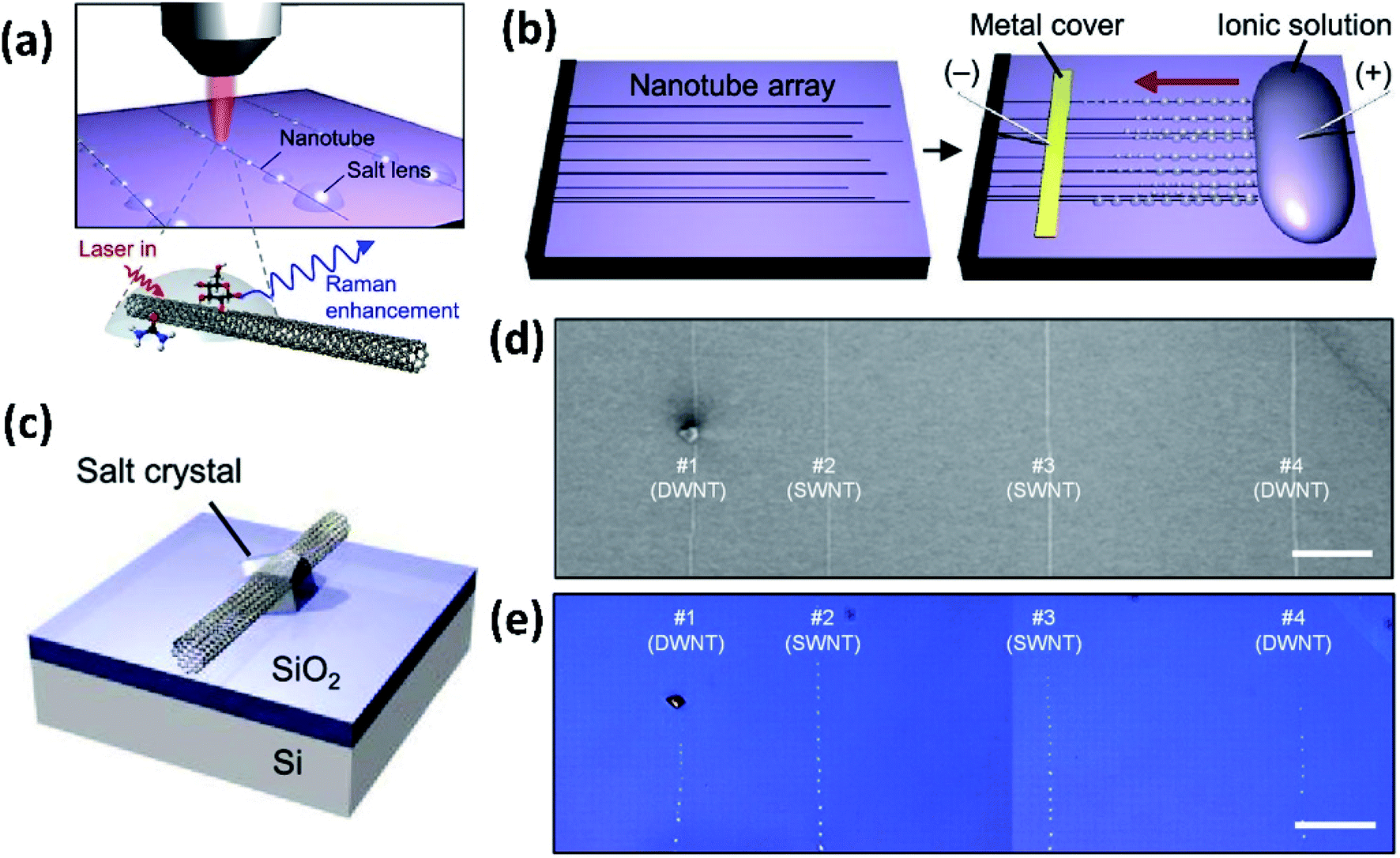 | ||
| Fig. 7 (a) Schematic diagram of the optical visualization and Raman enhancement of CNTs achieved by NaCl nanocrystals. (b) Experimental platform for forming NaCl nanocrystals along CNTs. (c) Schematic of the NaCl crystal. (d) SEM image of four CNTs before being decorated with NaCl crystals. Scale bar: 20 μm. (e) Optical image of salt crystals formed along all four CNTs. Scale bar: 20 μm. | ||
The NaCl crystals, with a refractive index of ∼1.54 and a plano-convex shape, served as micro/nanolenses to scatter more light to allow the decorated CNTs to be visualized under an optical microscope and to amplify the Raman scattering (Fig. 7c–e). It was demonstrated that the NaCl nanocrystal formation does not damage the CNTs and they can be easily and non-destructively removed by simply rinsing with water. In addition, this method can also help optically visualize other nanostructures of random CNT networks, silver nanowires, and graphene nanoribbons.
3. Substrate-assisted optical visualization
It is known that tiny samples supported on substrates could be distinguished upon light irradiation as long as the contrast between the sample and substrate is sufficiently obvious, arising from their different scattering abilities. Therefore, apart from the decoration methods discussed above, it is also effective to modify the substrates to gain improved scattering, which thus generates stronger contrast. In this section, we introduce several substrate-assisted visualization technologies.Du et al. developed a VCA reverse display technique which employs condensed water droplets as the image pixels on hydrophilic/hydrophobic surfaces for anti-counterfeiting applications.34 In a typical procedure, a hydrophobic silicon wafer was first treated with O2 plasma and a trimethylchlorosilane (TMCS) or perfluorooctyltrichlorosilane (PFTS) self-assembled monolayer with given patterns to obtain hydrophilicity, and then the supersaturated water vapor introduced onto the wafer selectively formed nanosized water droplets on the patterned domain and grew into larger ones, which could thus scatter more light to visualize the outlines of the patterns with the naked eye (Fig. 8a and b).
 | ||
| Fig. 8 (a) Contact angles on various silicon wafers measured immediately after treatment with: (i) untreated Si wafer, (ii) O2 plasma, (iii) TMCS, and (iv) PFTS. (b) Microscopic images of water droplets condensed on a “dragon head” patterned Si wafer surface which was treated with O2 plasma, TMCS and PFTS, respectively. Scale bar: 500 μm. (c) CNTs enhance the HF etching of SiO2, producing a nanoscale trench around itself. (d) Change of optical interference (e.g., red vs. blue) makes the trench visible under an optical microscope. (e) Optical micrograph of two trenches produced by the CNT-enhanced HF etching of SiO2. (f, g) AFM image mosaic and optical micrograph of the same area of a silicon wafer, respectively. The two sets of arrows indicate the same location. | ||
Novak et al. found that individual CNTs supported on SiO2/Si substrates could locally facilitate the HF vapor etching of SiO2 to produce a trench along the CNTs, benefiting from the enhancement of water adsorption of CNTs. The depths of the trenches ranged from several to several tens of nanometers, which could be observed under a conventional optical microscope due to the change in optical interference in the SiO2 layer, allowing the associated CNT to be located (Fig. 8c–g).35 The shape and contrast of the trench depended on its depth as well as the thickness of the SiO2 layer, although the quantitative relationship has not been determined yet.
4. Fluorescence visualization of 1-D CNTs and 2-D graphene
Visualization of nanostructures based on fluorescence generally benefits from long-wavelength optical and near infrared (IR) imaging materials. In this section, we introduce the common methods applied on CNTs and graphene nanostructures for optical visualization.4.1 Fluorescence visualization of CNTs by fluorophore coating
Fluorescent materials, a large family of materials, can be divided into two categories of inorganic and organic groups, and each member has its advantages and drawbacks.36Compared with organic fluorescent materials, inorganic fluorescent agents have rarely been used as a coating. CdSe–ZnS quantum dots were reported as an inorganic coating on CNTs to realize the fluorescence visualization.37 In a typical experiment, CNTs were first dispersed in a sodium-dodecyl-sulfonate (SDS) solution and then mixed with CdSe–ZnS core–shell nanocrystals functionalized with mercaptoacetic acid, during which CdSe–ZnS nanocrystals arrange themselves on the sidewalls of CNTs due to the electrostatic interaction between zinc ions and electronegative oxygen atoms/anions, allowing the fluorescence visualization of different cluster sizes of CNTs in aqueous solution under optical microscopes (Fig. 9a–d).
 | ||
| Fig. 9 (a) Fluorescence and (b) transmitted brightfield images of individual CNTs and their ropes. (c) Transmission electron micrograph of QDs attached to the sidewall of a typical CNT–rope. (d) Schematic illustration of the coordination between the QDs and CNTs. (e) Electron microscopy of PVP-FL-coated CNTs prepared at a 0.2% CNT/PVP ratio (0.4% SDS). (f) Combined light and fluorescence microscopy image of PVP-coated nanotube bundles deposited on a glass slide. (g) Light microscopy image of the same bundles. Scale bar, 7 μm. (h) Individual fluorescent CNTs are only seen using fluorescence detection. Scale bar, 4 μm. (i, j) Epifluorescence images of CNTs stained with PSE. Scale bar, 1 μm. (k) Fluorescence microscope image of PDSiAzep/SWNTs trapped between the electrodes (shown in the circle). | ||
In contrast, organic fluorescent materials offer more choices for coating. For example, CNTs could be fluorescently observed and labeled by coating them with a polymer layer of vinylpyrrolidone (PVP-1300) several nanometers thick.38 PVP-covered SWNTs were formed by mixing a CNT suspension stabilized in SDS with PVP-1300 in water under specific conditions, during which multiple fluorophores attached to single CNTs, assembling into unique composite fluorophores (Fig. 9e–h). Thus, such CNTs could serve as unique fluorescent probes for biological detection of single molecule events.
In addition, a PSE (1-pyrenebutanoic acid, succinimidyl ester)-based staining methodology was exploited to optically visualize and characterize individual CNTs in aqueous solutions with a fluorescence microscope, with the advantage that PSE not only shows strong luminescence in solution but also can noncovalently attach to CNT sidewalls through molecular adsorption which does not damage the geometric and electronic configuration of CNTs (Fig. 9i and j).39,40 Therefore, this technique offers a simple tool for the in situ and noninvasive observation and characterization of CNTs and potentially for its bio hybrid structures.
Besides, a silicon-based polymer PDSiAzep has also been reported as a modifier to fluorescently activate CNTs, which consequently enabled their distinct visualization in solvents by fluorescence microscopy and eased their detection and manipulation with high sensitivity under a light microscope (Fig. 9k).41
4.2 Fluorescence visualization by modifying the substrates
Graphene has been demonstrated to be a highly efficient quencher that can strongly quench the emission of nearby dye molecules through energy transfer.42,43 Taking advantage of the quenching effect, graphene-based materials could be easily imaged on a fluorescent carrier due to their distinct contrast under a fluorescence microscope. However, research studies focusing on this have not been reported much to date.Treossi et al. reported that graphene oxide (GO) could be imaged on silicon oxide, quartz or glass through quenching the fluorescence of a thiophene-based dye (T4), covalently tethered to the substrates through a microwave-promoted silanization reaction.44 Under UV excitation (λexc = 330–380 nm), the functional T4 layer exhibited intense green emission while the emission of the GO domain was greatly quenched, forming high contrast that enabled the imaging of GO (Fig. 10a and b).
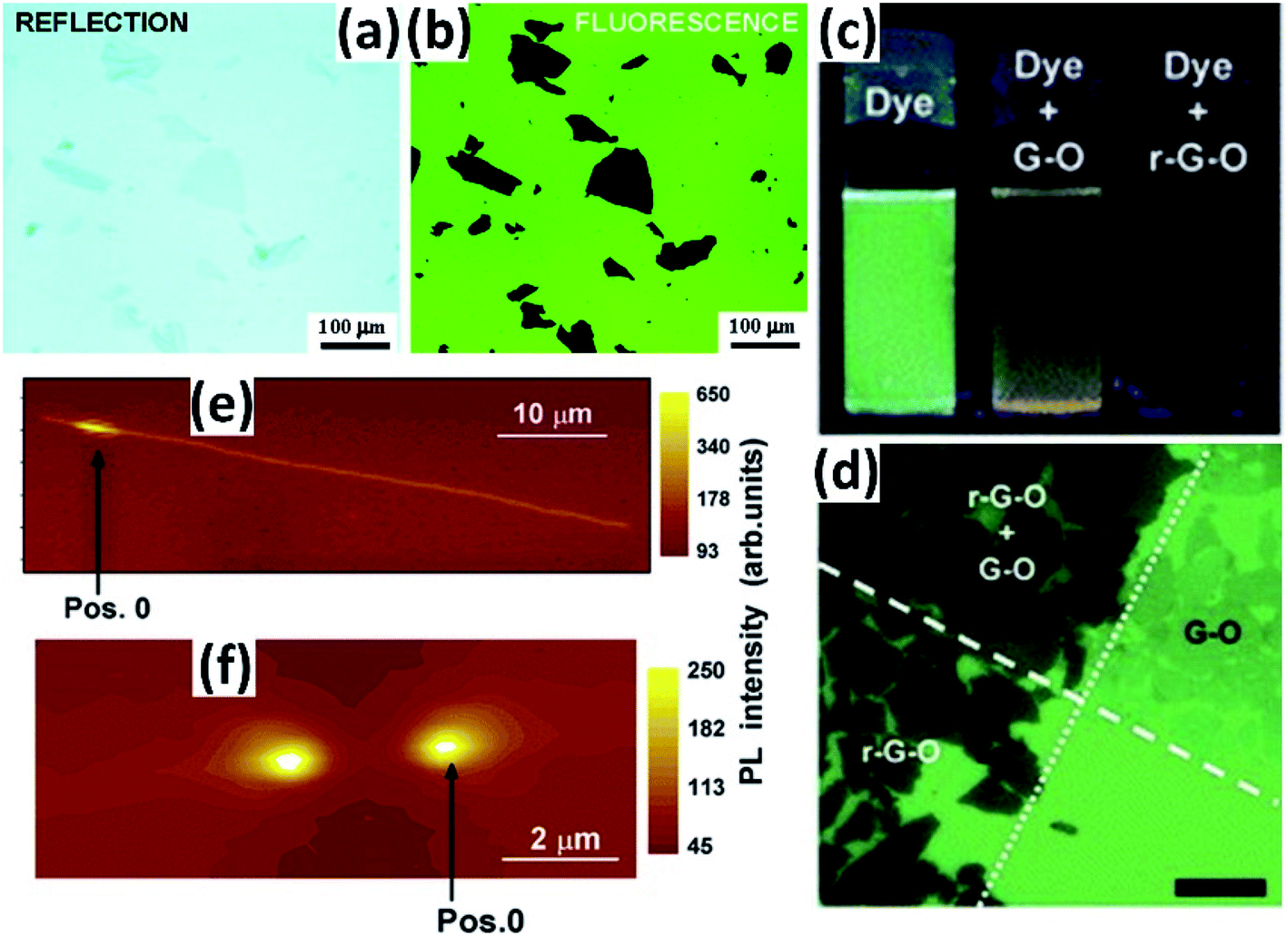 | ||
| Fig. 10 (a) Optical microscope image of GO sheets on T4-functionalized, 300 nm thick SiOx. (b) Fluorescence image of the same area. (c) A camera image showing strong emission quenching upon addition of G-O and r-G-O to a fluorescein solution. (d) Visualizing of a cross-deposited G-O/r-G-O sample on glass coverslip based single atomic layers by fluorescence quenching microscopy (FQM). Scale bar: 25 μm. (e) PL image of partially luminescent CNTs. The bright emission stripe in the upper left corner corresponds to a nanotube segment suspended over the trench. (f) Expanded PL image of a trench crossed by a CNT. | ||
Taking a similar approach, Kim et al. broadened the organic dyes to red, green and blue fluorescent ones, which could be easily removed by washing without disrupting the underlying sheets. They also demonstrated that it was feasible for arbitrary substrates even in solution, due to the non-functionalized surface.45 It is seen that the fluorescence quenching microscopy method can easily image these 2D sheets and greatly broaden the scope of single layer device fabrication (Fig. 10c and d).
Unlike the former cases, another substrate-assisted fluorescence visualization technique of CNTs was presented by etching trenches into the substrate.46 The trenches produced a direct comparison of the photoluminescence (PL) properties of air-suspended (across the trenches) and on-SiO2 segments of the CNTs, contributing to observable imaging (Fig. 10e and f). Besides, by acquiring PL maps at different locations along a CNT, the (n, m) structure as well as the mechanical strain or some deformations of the CNT could be checked and revealed.
4.3 Fluorescence visualization with near-infrared microscopy of CNTs
CNTs can exhibit a number of excitation bands from 600 to 800 nm and emissions from 950 to 1300 nm falling in the near-infrared (NIR) region, which thus offers another tool for detecting and characterizing CNTs with the help of NIR fluorescence microscopy at the macroscale.36 Typically, this method is combined with polarization measurements and emission spectroscopy to compensate for the limited spatial resolution of ca. 1 μm, and more preferably, to provide (n, m)-level identification of pristine semiconducting CNTs, which shows distinct advantages among the established techniques above. Alternatively, narrow-band optical filters can be added to generate (n, m)-selected images, for example, the inhomogeneous interactions of the CNT with its environment and the spatial consistency of the (n, m) structure can be revealed and checked by the spectral properties of different segments within longer CNTs. It is also notable that NIR imaging is applicable in a variety of media, such as water, SDBS (sodium dodecyl benzene sulfonate), and PVP solutions.47 To date, however, the NIR imaging for CNTs has not been studied much, and its advantages of simplicity, non-invasion, versatility of the sample environment and chirality identification make it a fascinating substitute.5. Facile imaging of CNTs based on the optical phenomenon
5.1 Rayleigh scattering imaging
Taking advantage of the unique band structures of CNTs, Rayleigh scattering imaging is performed using a white light incident beam in a dark-field configuration. Thus, the scattered spectra will reveal chirality and diameter information of the illuminated CNTs. Based on the Kataura plot shown in Fig. 11, CNT optical transitions in the visible light range (1.7–3.2 eV) should be sufficient to identify almost all CNTs with diameters between 1.5 and 2.5 nm and little scattered chirality outside this range.48 The first instance of CNT imaging by Rayleigh scattering was reported by Sfeir et al. in 2004 using a confocal microscope setup and a white-light supercontinuum excitation source. In order to circumvent substrate scattering, slits were etched in the Si/SiO2 substrate and imaging was performed on suspended CNTs.49 However, this imaging configuration was restricted severely by the limited spatial resolution of the setup and the observable portion of the CNTs was also limited to the small portion illuminated by the incident beam. | ||
| Fig. 11 (a) Refractive index matching imaging setup and the corresponding false color image; (b) refractive index matching/IDEE imaging configuration and real color image obtained in real time. | ||
Subsequent studies introduced the strategy of using real refractive index matching media to mitigate substrate scattering and allow in situ imaging of CNTs. The detection setup presented by Joh et al. utilizes a layer of glycerol on the CNT sample to realize in situ Rayleigh imaging (Fig. 11b). Glycerol (n ∼ 1.47) was chosen for its close real refractive index to quartz (n ∼ 1.54) in order to minimize photon scattering near the CNT/substrate interface.50 The glycerol layer was then sandwiched with a glass coverslip, and the incident beam was introduced from below the sample via a dark-field condenser at an angle such that the incident beam would be reflected at the coverslip/air interface via total internal reflection. This setup guaranteed that no incident light would enter the objective lens. The monochromatic incident beam (bandwidth = 20 nm) varied from 450–850 nm as a CCD detector with a high NA objective lens rastered across the image area. The resulting image was falsely colored based on resonance peak locations for the spectra at each pixel. Despite the short integration time per frame, this hyperspectral approach allowed for the characterization of intensity peak locations and widths. The full spectrum at each pixel allowed for the characterization of individual CNTs in multi-walled CNTs (MWCNTs) and CNT bundles. Red and blue shifts in resonance peaks were also observed resulting from intertube coupling effects.
The first real time, true color imaging of CNTs was realized by Wu et al. (Fig. 11a)51 utilizing the previously reported refractive index matching strategy in conjunction with an interface dipole enhancement effect (IDEE). Rayleigh scattering from CNTs on quartz and Si/SiO2 substrates was imaged in a wide-field setup. The posited IDEE required CNTs to be surrounded by a thin dielectric layer of high refractive index with no strong inherent Rayleigh scattering in the target spectrum. However, this technique also has its drawbacks. First, due to the size limitation of the visible spectrum, large diameter or multi-walled CNTs can't be detected. Second, the wide-field collection mode cannot provide enough information to identify the individual properties of bundled or multi-walled CNTs. Third, the use of refractive index matching media such as glycerol will restrict the handling of CNTs during imaging. Even after imaging, the medium must be removed with organic solvents by soaking or rinsing.
Havener et al. developed deep-ultraviolet resonance imaging of CNTs.52 The shorter wavelength ultraviolet light could enhance spatial resolution of the system to obtain a resonance peak shared by all CNTs in this region. Another approach for improving the imaging effect is modifying the sample preparation. Ideally, a high resolution, robust, and clean method enables the direct observation of CNTs in air. Refractive index matching and IDEE techniques require the immersion of the CNT samples in a liquid such as glycerol or water. In the former case, further use of the CNT samples requires a lengthy cleaning process to remove the liquid medium without damaging the tube or introducing impurities.
5.2 Raman scattering imaging
Like Rayleigh scattering, optical Raman imaging has inherent limitations due to the band structures of CNTs. For example, single-walled CNTs exhibit several Raman scattering modes include the radial breathing mode (RBM), G-band, and D-band.53 The RBM frequency is indicative of the CNT diameter. Most early Raman imaging techniques involved confocal microscopy setups where the image are was scanned in its entirety and the Raman spectrum was obtained for each pixel.54 Although this method provides sufficient spectral information, it comes at the cost of imaging speed. The resulting image is usually colored based on the intensity of a specific resonant mode such as the G-band. Another consideration in Raman imaging is that laser intensity must be controlled to prevent damage to the substrate.Compared with Rayleigh scattering, Raman scattering presents higher intensity and signal-noise ratio in the imaging process. The inelastic nature of Raman scattering coupled with the well documented G-band wavelengths gave rise to a strategy of selectively filtering the incident light and detecting only the G-band frequency instead of the entire spectrum for each point.55
Current optical spectroscopic imaging techniques have achieved great advances such as real time monitoring of CNT growth, real time and real color imaging, etc.51,56 However, these optical approaches are still fundamentally limited by the Abbe diffraction limit. To date, there has been no study applying the principles or super-resolution microscopy breaking the resolution limit of an optical microscope to perform the imaging of CNTs.
5.3 Polarized light imaging
Diameters of CNTs are several orders of magnitude smaller than the illumination beam size, which makes their absorption signal easily blurred by the fluctuation of the light. However, Liu et al. introduced a polarized microscopy method with high-throughput imaging and spectroscopy, which increased the amplitude of the optical signal of CNTs by two orders of magnitude (Fig. 12a).57 When illuminating a CNT on a substrate by visible light, there is interference between the CNT-scattered electric field ENT and the substrate-reflected electric field Er at the detector, which makes the optical contrast of a CNT enhanced in a reflection configuration.58 Using this technique, CNTs can be clearly observed under optical microscopy, of which the resolution is comparable with that of SEM (Fig. 12b). On top of this, chirality profiling of CNTs can be completed. The M/S can be determined from the color imaging by polarized light imaging. This technique benefits the study of CNT growth theory.57 Zhao et al. reported the phenomenon of self-termination in the etching process of CNTs using a hot-wall chemical reactor equipped with a polarized light microscope.59 Vincent et al. improved this method by setting up a new model with the consideration of depolarization to make the polarized imaging more accurate.60 | ||
| Fig. 12 (a) Schematic of the high-throughput optical microscope with a polarizer, (b)–(d) real-time optical imaging of individual CNTs on a substrate or in a device. Direct optical images of the individual CNTs (b) on a fused-silica substrate, (c) in a back-gated field-effect transistor device (with two gold electrodes), or (d) located partly under an Al2O3 dielectric layer, with an integration time of about 20 ms. (e)–(g) Schematics of CNTs corresponding to the optical images in (b)–(d). | ||
6. Modified optical microscopes for nanomaterial visualization
Apart from the post-treatment of nanomaterials, modified optical microscopes are also widely used for visualizing nano- or micro-scale materials, and they successfully avoid radiation damage from conventional electron microscopes. In this section, modified optical microscopes and the corresponding changes in their light paths are discussed.Due to the resolution limitation in the wavelength of the light beam the nanomaterial is not clearly seen under such conditions. Microscopes combined with other apparatus such as a polarizer, microsphere, etc., could solve this problem or provide more information on the spatial distribution and quality of the material included. Liu et al. reported that a high-throughput optical imaging technique with a polarizer to change the light path forms a contrast between a CNT and the substrate, providing a clear image of the CNT.57
Besides, modified microscopes provide more information to enable its manipulation or obtain other properties. Brenner et al. reported that hyperspectral microscopy which combines hyperspectral imaging with state-of-the-art computer software provides more axial information.61 Using this technique, a multi-constituent material enables easier and rapid identification of nanomaterials such as CNTs.62 In addition, Sun et al. used a nonlinear microscope with coherent anti-Stokes Raman scattering spectroscopy (CARS), two-photon excitation fluorescence (TPEF) and second harmonic generation (SHG), which can not only clearly image the surface topography of graphene, but also characterize the quality of the material.63
What's more, the modified microscopes enable the observation and three-dimensional characterization, which have rarely been investigated in recent studies. Leong-Hoi et al. introduced a high-resolution microsphere-assisted interference microscope to characterize the interface of the gratings, which showed a comparable imaging result with that from an atomic force microscope (Fig. 13).64 The microsphere served as a tool for optical magnification. Besides, phase-shifting interferometry was employed to obtain more axial information. Moreover, Igor et al. combined optical microscopy with scanning probe nanotomography to reconstruct the 3D structure of a sample at the nanoscale.65 The novel technique is expected to provide important data on the structural organization of biomedical materials, which helps in quality control of the nanotechnological fabrication process.
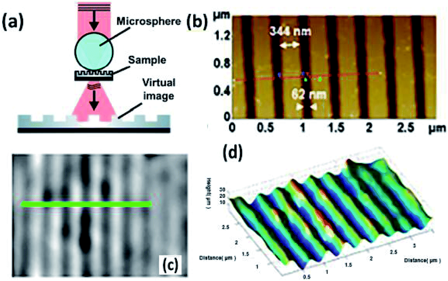 | ||
| Fig. 13 (a) Schematic of high-resolution microsphere-assisted interference microscopy, (b) measurements of the 400 nm periodic grating with AFM, (c, d) measurements of the 400 nm periodic grating with AFM, (c) surface topography and (d) 3D measurement through the microsphere.62 | ||
7. Summary and outlook
In this review, we briefly summarized several techniques for the optical visualization of nanomaterials, e.g., vapor condensation-assisted visualization, NP-assisted visualization, substrate-assisted visualization and fluorescence visualization. Applications of these techniques in the imaging of CNTs and other nanomaterials were also included. Besides, state-of-the-art strategies and methods for modifying microscopes were further discussed to shed light on the synergistic development of optical microscopy and nanomaterials.In the research on nanomaterials, because of their tiny sizes, a key and challenging point is their fast location, identification, and manipulation. Even in electron microscopes such as SEM, TEM, etc., the sample must be treated under vacuum and airtight conditions so that the information on the morphology and other properties could be available, which has many disadvantages. On the one hand, it is hard to carry out the operation under such conditions. On the other hand, the sample is destroyed to some extent after the pre-treatment for electron microscopy. Based on this, optical visualization enables manipulation under normal conditions without damaging these samples.
We deeply believe that the optical visualization of nanomaterials still has large room for development, and our perspectives on the future of this field are listed as follows. (i) The optical visualization of 1-D and 2-D nanostructures (e.g., CNTs and graphene) has been extensively explored, while the visualization of 0-D and 3-D nanostructures is much less reported. The dimensions of the samples are expected to be largely expanded with the assistance of advanced imaging techniques. (ii) The vapor condensation method enables corresponding manipulation such as stretching under normal conditions, which could enhance the testing difficulty for the nanomaterials, the volatile substance included. However, the vapor condensation method allows virtual imaging under an optical microscope, which could be the next point to transform virtual imaging directly or indirectly to true imaging. (iii) The combination of the optical microscope with other techniques could attract some interest. For example, we could obtain the optical properties and thermal properties simultaneously under a virtual optical microscope equipped with a thermal performance testing device. The advancement of other techniques also pushes optical visualization development.
Conflicts of interest
There are no competing interests to declare.Acknowledgements
This work was supported by the National Natural Science Foundation of China (Grant No. 51872156 and 22075163).References
- M. J. Allen, V. C. Tung and R. B. Kaner, Chem. Rev., 2010, 110, 132–145 CrossRef CAS.
- R. H. Baughman, A. A. Zakhidov and W. A. de Heer, Science, 2002, 297, 787–792 CrossRef CAS.
- F. R. Yao, C. Chen, C. Liu, J. Zhang, F. Wang and K. H. Liu, Chem.–Eur. J., 2017, 23, 3703–9710 Search PubMed.
- H. Bai, L. Wang, J. Ju, R. Sun, Y. Zheng and L. Jiang, Adv. Mater., 2014, 26, 5025–5030 CrossRef CAS.
- N. Miljkovic, R. Enright, Y. Nam, K. Lopez, N. Dou, J. Sack and E. N. Wang, Nano Lett., 2013, 13, 179–187 CrossRef CAS.
- Q. Zhang, M. He, X. Zeng, K. Li, D. Cui, J. Chen, J. Wang, Y. Song and L. Jiang, Soft Matter, 2012, 8, 8285 RSC.
- G. P. Lopez, H. A. Biebuyck, C. D. Frisbie and G. M. Whitesides, Science, 1993, 260, 647–649 CrossRef CAS.
- R. N. Leach, F. Stevens, S. C. Langford and J. T. Dickinson, Langmuir, 2006, 22, 8864–8872 CrossRef CAS.
- K. G. Lee, B. G. Choi, B. I. Kim, T. Shyu, M. S. Oh, S. G. Im, S. J. Chang, T. J. Lee, N. A. Kotov and S. J. Lee, Adv. Mater., 2014, 26, 6119–6124 CrossRef CAS.
- R. Raj, S. Adera, R. Enright and E. N. Wang, Nat. Commun., 2014, 5, 4975 CrossRef CAS.
- J. Wang, T. Li, B. Xia, X. Jin, H. Wei, W. Wu, Y. Wei, J. Wang, P. Liu, L. Zhang, Q. Li, S. Fan and K. Jiang, Nano Lett., 2014, 14, 3527–3533 CrossRef CAS.
- J. Wang, P. Liu, B. Xia, H. Wei, Y. Wei, Y. Wu, K. Liu, L. Zhang, J. Wang, Q. Li, S. Fan and K. Jiang, Nano Lett., 2016, 16, 4102–4109 CrossRef CAS.
- X. Zhang, L. Song, L. Cai, X. Tian, Q. Zhang, X. Qi, W. Zhou, N. Zhang, F. Yang, Q. Fan, Y. Wang, H. Liu, X. Bai, W. Zhou and S. Xie, Light: Sci. Appl., 2015, 4, e318 CrossRef CAS.
- R. Zhang, B. Liu, A. Yang, Y. Zhu and Y. Cui, Nano Lett., 2018, 18, 1130–1138 CrossRef CAS.
- K. Xia, M. Jian, W. Zhang and Y. Zhang, Adv. Mater., 2016, 3, 1500674 Search PubMed.
- D. L. Duong, G. H. Han, S. M. Lee, F. Gunes, E. S. Kim, S. T. Kim, H. Kim, Q. H. Ta, K. P. So, S. J. Yoon, S. J. Chae, Y. W. Jo, M. H. Park, S. H. Chae, S. C. Lim, J. Y. Choi and Y. H. Lee, Nature, 2012, 490, 235–239 CrossRef CAS.
- E. Huber and M. Frost, Aqua, 1998, 47, 87–94 CrossRef CAS.
- M. I. Mishchenko, L. D. Travis and A. A. Lacis, Scattering, Absorption, and Emission of Light by Small Particles, Cambridge University Press, 2002 Search PubMed.
- R. Zhang, Q. Wen, W. Qian, D. S. Su, Q. Zhang and F. Wei, Adv. Mater., 2011, 23, 3387–3391 CrossRef CAS.
- R. Zhang, Y. Zhang, Q. Zhang, H. Xie, H. Wang, J. Nie, Q. Wen and F. Wei, Nat. Commun., 2013, 4, 1727 CrossRef.
- R. Zhang, Z. Ning, Y. Zhang, Q. Zheng, Q. Chen, H. Xie, Q. Zhang, W. Qian and F. Wei, Nat. Nanotechnol., 2013, 8, 912–916 CrossRef CAS.
- R. Zhang, Z. Ning, Y. Zhang, H. Xie, Q. Zhang, W. Qian, Q. Chen and F. Wei, Nanoscale, 2013, 5, 6584–6588 RSC.
- R. Wang, T. Wang, T. Hong and Y.-Q. Xu, Nanotechnology, 2018, 29, 345205 CrossRef.
- C. Liu, H. Hong, Q. Wang, P. Liu, Y. Zuo, J. Liang, Y. Cheng, X. Zhou, J. Wang, Y. Zhao, J. Xiong, B. Xiang, J. Zhang and K. Liu, Nanoscale, 2019, 11, 17195–17200 RSC.
- M. Zhao, Y. Ye, Y. Han, Y. Xia, H. Zhu, S. Wang, Y. Wang, D. A. Muller and X. Zhang, Nat. Nanotechnol., 2016, 11, 954–959 CrossRef CAS.
- M. Jian, H. Xie, Q. Wang, K. Xia, Z. Yin, M. Zhang, N. Deng, L. Wang, T. Ren and Y. Zhang, Nanoscale, 2016, 8, 13437–13444 RSC.
- S. Huang, Y. Qian, J. Chen, Q. Cai, L. Wan, S. Wang and W. Hu, J. Am. Chem. Soc., 2008, 130, 11860–11861 CrossRef CAS.
- Y. Qian, S. Huang, F. Gao, Q. Cai, L. Zhang and W. Hu, J. Phys. Chem. C, 2009, 113, 6983–6988 CrossRef CAS.
- H. Chu, R. Cui, J. Wang, J. Yang and Y. Li, Carbon, 2011, 49, 1182–1188 CrossRef CAS.
- H. Chu, J. Wang, L. Ding, D. Yuan, Y. Zhang, J. Liu and Y. Li, J. Am. Chem. Soc., 2009, 131, 14310–14316 CrossRef CAS.
- G. Zeevi, M. Shlafman, T. Tabachnik, Z. Rogachevsky, S. Rechnitz, I. Goldshtein, S. Shlafman, N. Gordon, G. Alchanati, M. Itzhak, Y. Moshe, E. M. Hajaj, H. Nir, Y. Milyutin, T. Y. Izraeli, A. Razin, O. Shtempluck, V. Kotchtakov and Y. E. Yaish, Nat. Commun., 2016, 7, 12153 CrossRef CAS.
- Y. T. Kim, H. Min, M. S. Strano, J. H. Han and C. Y. Lee, Nano Lett., 2019, 8911–8919 Search PubMed.
- J. J. Pigeon, S. Y. Tochitsky, E. C. Welch and C. Joshi, Opt. Lett., 2016, 41, 3924–3927 CrossRef CAS.
- X. Du, J. Wang, H. Cui, T. Tang and T. Wu, Proceedings of the 11th IEEE Annual International Conference on Nano/Micro Engineered and Molecular Systems (NEMS), 2016, pp. 17–20 Search PubMed.
- M. A. Novak, S. Surwade, J. Prokop, K. Bolotin, J. Hone, L. Brus, C. Nuckolls and H. Liu, J. Am. Chem. Soc., 2014, 136, 8536–8539 CrossRef CAS.
- V. Pansare, S. Hejazi, W. Faenza and R. K. Prud'homme, Chem. Mater., 2012, 24, 812–827 CrossRef CAS.
- S. Chaudhary, J. H. Kim, K. V. Singh and M. Ozkan, Nano Lett., 2004, 4, 2415–2419 CrossRef CAS.
- V. V. Didenko, V. C. Moore, D. S. Baskin and R. E. Smalley, Nano Lett., 2005, 5, 1563–1567 CrossRef CAS.
- R. J. Chen, Y. Zhang, D. Wang and H. Dai, J. Am. Chem. Soc., 2001, 123, 3838–3839 CrossRef CAS.
- J.-W. Kim, N. Kotagiri, J.-H. Kim and R. Deaton, Appl. Phys. Lett., 2006, 88, 213110 CrossRef.
- K. Otobe, H. Nakao, H. Hayashi, F. Nihey, M. Yudasaka and S. Iijima, Nano Lett., 2002, 1157–1160 CrossRef CAS.
- R. S. Swathi and K. L. Sebastian, J. Chem. Phys., 2008, 129, 054703 CrossRef CAS.
- R. S. Swathi and K. L. Sebastian, J. Chem. Phys., 2009, 130, 086101 CrossRef CAS.
- E. Treossi, M. Melucci, A. Liscio, M. Gazzano, P. Samorì and V. Palermo, J. Am. Chem. Soc., 2009, 131, 15576–15577 CrossRef CAS.
- J. Kim, L. J. Cote, F. Kim and J. Huang, J. Am. Chem. Soc., 2009, 132, 260–267 CrossRef.
- O. Kiowski, S.-S. Jester, S. Lebedkin, Z. Jin, Y. Li and M. M. Kappes, Phys. Rev. B, 2009, 80, 075426 CrossRef.
- S. M. B. Dmitri, A. Tsyboulski and R. Bruce Weisman, Nano Lett., 2005, 5, 975–979 CrossRef.
- M. S. Strano, J. Am. Chem. Soc., 2003, 125, 16148–16153 CrossRef CAS.
- M. Y. Sfeir, F. Wang, L. M. Huang, C. C. Chuang, J. Hone, S. P. O'Brien, T. F. Heinz and L. E. Brus, Science, 2004, 306, 1540–1543 CrossRef CAS.
- D. Y. Joh, L. H. Herman, S. Y. Ju, J. Kinder, M. A. Segal, J. N. Johnson, G. K. L. Chan and J. Park, Nano Lett., 2011, 11, 1–7 CrossRef CAS.
- W. Y. Wu, J. Y. Yue, X. Y. Lin, D. Q. Li, F. Q. Zhu, X. Yin, J. Zhu, J. T. Wang, J. Zhang, Y. Chen, X. H. Wang, T. Y. Li, Y. J. He, X. C. Dai, P. Liu, Y. Wei, J. P. Wang, W. Zhang, Y. D. Huang, L. Fan, L. N. Zhang, Q. Q. Li, S. S. Fan and K. L. Jiang, Nano Res., 2015, 8, 2721–2732 CrossRef CAS.
- R. W. Havener, A. W. Tsen, H. C. Choi and J. Park, NPG Asia Mater., 2011, 3, 91–99 CrossRef.
- A. Jorio, R. Saito, J. H. Hafner, C. M. Lieber, M. Hunter, T. McClure, G. Dresselhaus and M. S. Dresselhaus, Phys. Rev. Lett., 2001, 86, 1118–1121 CrossRef CAS.
- C. Y. Jiang, J. L. Zhao, H. A. Therese, M. Friedrich and A. Mews, J. Phys. Chem. B, 2003, 107, 8742–8745 CrossRef CAS.
- L. Zhang, L. Huang, S. P. O'Brien and Z. Yu, J. Phys. Chem. C, 2008, 112, 20118–20122 CrossRef CAS.
- K. Kaminska, J. Lefebvre, D. G. Austing and P. Finnie, Nanotechnology, 2007, 18, 6 CrossRef.
- K. H. Liu, X. P. Hong, Q. Zhou, C. H. Jin, J. H. Li, W. W. Zhou, J. Liu, E. G. Wang, A. Zettl and F. Wang, Nat. Nanotechnol., 2013, 8, 917–922 CrossRef CAS.
- R. F. Zhang, Y. Y. Zhang and F. Wei, Chem. Soc. Rev., 2017, 46, 3661–3715 RSC.
- Q. C. Zhao, F. R. Yao, Z. Q. Wang, S. B. Deng, L. M. Tong, K. H. Liu and J. Zhang, Adv. Mater., 2017, 29, 1701959 CrossRef.
- L. Monniello, H.-N. Tran, R. Vialla, G. Prévot, S. Tahir, T. Michel and V. Jourdain, Phys. Rev. B, 2019, 99, 115431 CrossRef CAS.
- G. A. Roth, S. Tahiliani, N. M. Neu-Baker and S. A. Brenner, Wiley Interdisciplinary Reviews-Nanomedicine and Nanobiotechnology, 2015, vol. 7, pp. 565–579 Search PubMed.
- F. Schwab, T. D. Bucheli, L. Camenzuli, A. Magrez, K. Knauer, L. Sigg and B. Nowack, Environ. Sci. Technol., 2013, 47, 7012–7019 CrossRef CAS.
- R. Li, Y. J. Zhang, X. F. Xu, Y. Zhou, M. D. Chen and M. T. Sun, Nanophotonics, 2018, 7, 873–881 CAS.
- A. Leong-Hoi, C. Hairaye, S. Perrin, S. Lecler, P. Pfeiffer and P. Montgomery, Phys. Status Solidi A, 2018, 215, 1700858 CrossRef.
- K. E. Mochalov, A. E. Efimov, A. Bobrovsky, I. I. Agapov, A. A. Chistyakov, V. Oleinikov, A. Sukhanova and I. Nabiev, ACS Nano, 2013, 7, 8953–8962 CrossRef CAS.
Footnote |
| † These authors contributed equally to this work. |
| This journal is © The Royal Society of Chemistry 2021 |