
 Open Access Article
 This Open Access Article is licensed under a Creative Commons Attribution-Non Commercial 3.0 Unported Licence
Flexible fabrication of new-type porous anodic alumina membranes with tunable geometric features by low-cost nanoimprint lithography†
Xianzhong
Lang
 *ab,
Xudong
Wang
b,
Ji
Ma
b and
Teng
Qiu
a
*ab,
Xudong
Wang
b,
Ji
Ma
b and
Teng
Qiu
a
aSchool of Physics, Southeast University, Nanjing 211189, P. R. China
bSchool of Microelectronics and Control Engineering, Changzhou University, Changzhou 213164, P. R. China. E-mail: xzlang@cczu.edu.cn
First published on 24th March 2021
Abstract
A novel process for the flexible fabrication of new-type porous anodic alumina (PAA) membranes with tunable geometric features is described. In this process, the conventional PAA template as a cost-effective nanoimprint stamp is employed to transfer the anti-structure nanopits onto aluminum sheet substrates, and the subsequent guided anodization of the pre-patterned substrates leads to new-type PAAs. By further adjusting the anode voltages of PAA stamps, imprinting pressures and guided anode voltages, a series of new-type PAAs with controlled para-pore spacing, surface topography and nanopore arrangement are achieved. The new-type PAAs provide a low-cost flexible option for the preparation of arrays with utility in photonic, electronic and magnetic devices.
Introduction
Porous anodic alumina (PAA), a typical self-ordered nanochannel material formed by anodization of aluminum (Al) in an appropriate acid solution, has stimulated considerable interest in recent years as an ideal template for a variety of utilizations, such as in photonic,1 electronic,2 photoelectric3 and energy storage devices.4,5 Usually the natural architecture of PAA is a hexagonal close-packed pattern of columnar cells, but it often lacks the versatility obtained by the direct self-organization method,6 which limits its applicability in the diverse design and synthesis of nanostructures.To solve this problem, non-hexagonal close-packed patterns of PAA, such as square, triangular, diamond and hybrid pattern pores or cells, have been achieved by pre-patterning the Al surface prior to anodization utilizing various lithography methods, including nanoimprint lithography (NIL),7 focused ion beam (FIB)8,9 and electron-beam lithography (EBL).10 Although these new-type PAAs are promising candidates for several nanoscale applications, untapped new-type PAAs remain to be explored for various potential applications in functional nanostructures, and the corresponding phenomenon and mechanism of the guiding process remain to be discussed for further designing and fabricating new-type PAAs.3,11,12 In particular, the influence of the topography of pre-patterns on guided anodization is not yet understood.
On the other hand, although these pre-patterning methods are advantageous to obtain well-defined pre-patterns, they usually face limitations in other aspects. For example, FIB and EBL have intrinsic drawbacks of high cost, low throughput and tedious fabrication processes. NIL is usually limited by hard imprinting stamps, which have the high cost associated with EBL or FIB and do not last long due to mechanical wear.13,14 These restrictions in terms of processing time and cost make it difficult to use them as sacrificial templates.15 As alternatives, some pre-patterning techniques with simpler and lower-cost processes have been used for the fabrication of PAA, such as nanosphere lithography (NSL),16–18 step and flash imprint lithography15 and soft nanoimprinting lithography.19 However, most of them mainly focus on fabricating conventional hexagonal PAA over large areas. Moreover, only one new-type PAAs with a 2D surface topography can be prepared by one-step press using the same imprint stamp.
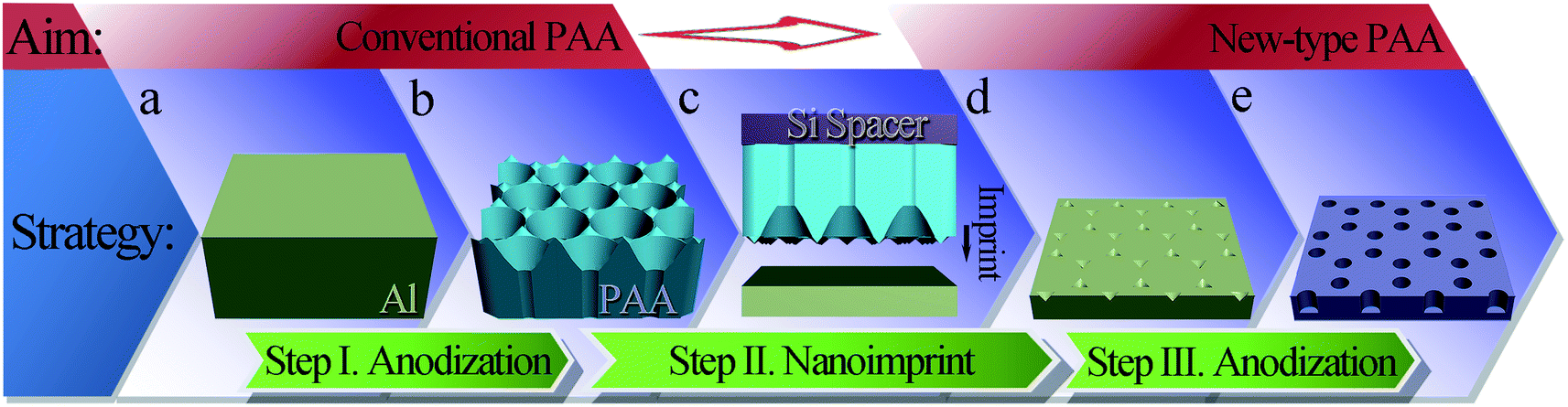
Herein, we demonstrate a novel process for the flexible fabrication of new-type PAA membranes with tunable geometric features by low-cost nanoimprint lithography. Besides the guided anodization of 2D pre-patterns with graphite lattice dotted nanopits, the guided anodization of complex 3D pre-patterns with convex nanoislands and graphite lattice dotted nanopits was carried out. The latter guided anodization and inhibitory effect of convex nanoislands are rarely discussed in previous literature. A series of new-type PAAs with 2D and 3D surface topographies, which are hard to obtain with the previous guided anodization, were prepared by one-step press using the same low-cost PAA stamp, respectively, only using simple and cost-effective equipment available to most researchers. Such a surface topography modulation opens the possibility of exploiting the new-type PAAs as templates for creating nanocomposites with 2D and 3D surface topographies. In addition, this technique has three distinct advantages over earlier approaches: (1) the desired para-pore spacing, surface topography and nanopore arrangement of the new-type PAA can be easily tailored by adjusting the anode voltage of PAA stamps (Vstamp), imprinting pressure and anode voltage of new-type PAAs (VPAA), respectively. (2) PAA stamp preparation is simple, mass producible and low cost (less than 2 dollars per cm2),14 and also compatible with new-type PAA preparation which further reduces the costs of new-type PAA production and chemical pollution reduction. (3) This technique has the potential to enlarge the anodization window which is important for fabricating PAAs with ultra-high density hexagonal pores.
Experimental section
Materials
Aluminum sheets were purchased from the General Research Institute for Nonferrous Metals (Beijing, China). Poly(methylmethacrylate) (950 PMMA A4) was obtained from MicroChem (Westborough, MA, USA). Acetone, ethanol, perchloric acid, oxalic acid, chromium trioxide, phosphoric acid and copper sulfate were all obtained from Sinopharm Chemical Reagent Co., Ltd (Shanghai, China). All reagents were used without further purification. Deionized water (POSEIDON-R70C, RSJ, Xiamen, USA) was used in the whole experiment.Characterization
Scanning electron microscopy (SEM) (Carl Zeiss Ultra Plus) and atomic force microscopy (AFM) (Veeco NanoScope V) in tapping mode under ambient conditions were used to investigate the nanostructures. The AFM probe was composed of a pyramidal tip with a length of 14–16 μm and a radius of curvature of 6 nm connected to a rectangular silicon cantilever with a 30 ± 5 nm thick aluminum reflex side coating. The nanoindentation measurements were made in air using an MTS Nano-Indenter XP instrument with a diamond Berkovich indenter. The indentation depth was smaller than one tenth of the oxide thickness to avoid influence of the substrate. Prior to the measurement, the projected area of the indenter was determined for the selected depth using a silica reference.Synthesis of PAA stamps
Aluminum sheets (99.99% pure, 30 mm × 30 mm × 0.5 mm) were degreased with acetone and electro-polished using a mixture of ethanol and perchloric acid with a volume ratio of 5![[thin space (1/6-em)]](https://www.rsc.org/images/entities/char_2009.gif) :1 under a constant direct current (dc) voltage of 15 V for 3 min to further remove surface contaminants (Fig. 1a). After rinsing in distilled water and drying, the aluminum sheets were anodized separately in a 0.5 M oxalic acid solution under a constant dc voltage of 30 V (40, 50 and 60 V) at 10 °C. In order to obtain an ordered nanopore array, a two-step anodizing process was adopted.21 PMMA was spin coated on the top surface of the PAA stamp. The aluminum base was removed in a saturated solution of copper sulfate by wet chemical etching, and the PAA stamps (Fig. 1b) were finally obtained by dissolving the PMMA in acetone.
:1 under a constant direct current (dc) voltage of 15 V for 3 min to further remove surface contaminants (Fig. 1a). After rinsing in distilled water and drying, the aluminum sheets were anodized separately in a 0.5 M oxalic acid solution under a constant dc voltage of 30 V (40, 50 and 60 V) at 10 °C. In order to obtain an ordered nanopore array, a two-step anodizing process was adopted.21 PMMA was spin coated on the top surface of the PAA stamp. The aluminum base was removed in a saturated solution of copper sulfate by wet chemical etching, and the PAA stamps (Fig. 1b) were finally obtained by dissolving the PMMA in acetone.
 | ||
| Fig. 1 Schematic illustrating the fabrication process of the new-type PAA: Step I. Synthesis of conventional PAA as nanoimprint stamps. Step II. Pattern transfer onto aluminum by NIL. Step III. Anodization of pre-patterned aluminum. (a) Pretreated Al sheets, (b) PAA stamp, (c) direct nanoimprint using PAA stamps, (d) Al sheets with pre-patterned graphite lattice concaves, (e) new-type PAA with graphite lattice pores. | ||
Nanoimprint process
The imprinting process was carried out by using a conventional oil-press-type imprinting instrument (Fig. 1c). The periodic hexagonal cells on the PAA stamp were transferred onto the Al sheet by mechanically pressing the stamp on the substrate. A self-adjusting mechanism was implemented on the imprinting equipment to ensure that the stamp and Al sheet remained parallel during the imprinting process. In order to obtain a tailored surface topography of the transferred pattern, different imprinting pressures were chosen. After the imprinting process, the PAA stamp was manually demolded with tweezers to reveal the designed Al pre-pattern (Fig. 1d).Anodization of the pre-patterned aluminum
The pre-patterned aluminum sheets were directly anodized separately in a 0.5 M oxalic acid solution under different constant dc voltages for 5 min at 10 °C (Fig. 1d and e).Results and discussion
Fig. 1 illustrates schematically the simple and cost-effective process for the fabrication of a typical new-type PAA membrane. The new-type PAA prepared by the pre-patterning method undergoes three steps. First, conventional PAAs were fabricated by anodizing Al sheets with a surface roughness of less than 3 nm (Fig. 1a and b). A two-step anodic process was utilized to improve the nanopore periodicity of the conventional PAAs. SEM observation (Fig. 2a) and the 3D AFM image (Fig. S1†) reveal a typical surface topography of a conventional PAA with periodic hexagonal cells and small protrusions along the surface of the pore wall. The sharp protrusions with nanotips of less than 10 nm and a para-protrusion spacing (Spr) of about 100 nm have periodical graphite lattice arrangements. It is favorable for the subsequent nanoimprinting because sharp protrusions are easier to press into the substrate at a smaller pressure. Furthermore, conventional PAAs have good mechanical properties (Fig. S2†), can be easily scaled up to contiguous areas cm2 in size (inset in Fig. 2a) and have the advantage of low cost manufacturing (less than 2 dollars per cm2).14 Second, the as-prepared PAAs were exploited as stamps in a standard imprinting process to obtain graphite lattice nanopits on Al sheets through replication (Fig. 1b–d).20 When the PAA stamp was mechanically pressed on the Al sheet at a pressure of 1.5 GPa for 30 s and at room temperature, anti-structure graphite lattice nanopits with nanometer precision could be obtained (Fig. 2b). The transferred nanopits show uniform shape, size and para-pit spacing (Spi). Finally, the as-prepared pre-patterned Al sheets were anodized under an appropriate anode voltage (28 V), which is discussed in the ESI (Fig. S3, S4 and Table S1†). Typical SEM images of the new-type PAA (Fig. 2c) show periodic graphite lattice pores with narrow size distributions. The mean diameter and para-pore spacing (Spo) are close to 17 nm and 107 nm, respectively.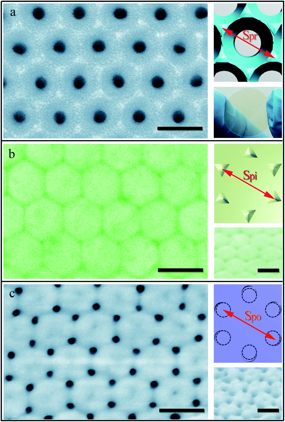 | ||
| Fig. 2 Representative SEM top views and the corresponding structure diagrams (upper inset) of the (a) PAA stamps (Vstamp = 40 V), (b) imprinted Al sheets (imprinting pressure = 1.5 GPa), and (c) new-type PAAs (VPAA = 28 V). The lower insets in (a), (b) and (c) show the corresponding optical photograph of the PAA stamp, SEM side views of the nanocap and new-type PAA, respectively. The scale bar represents 100 nm. | ||
Moreover, the results indicate that the nanopits on the Al sheet can effectively guide the anodization of alumina nanopores. That is to say, Spr dictates Spi and subsequent Spo. Therefore, Spo can further be tuned by adjusting Spr in Step I. Fig. 3a shows the schematic illustrations of Spr tailored using Vstamp. Experimentally, when Vstamp increases from 30 to 60 V, Spr linearly increases from 73 to 151 nm.20 After anodization for 5 min under different appropriate anode voltages (see Table S2†), all anodized nanopore arrays maintain the ordered graphite lattice arrangement while the Spo grows from 76 to 156 nm (Fig. 3b). As expected, Spo meets the linear proportional relationship with Spo:Vstamp = 2.5 nm V−1. Accordingly, this technique can effectively tailor the densities of the nanopores between 2 × 10¹⁰ and 1.4 × 1011 cm−2.
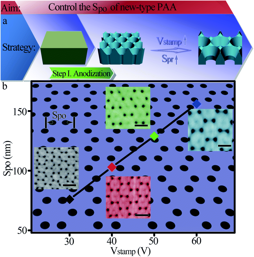 | ||
| Fig. 3 New-type PAA with graphite lattice nanopores tuned using Vstamp in Step I. (a) Schematic of PAA stamps tailored using Vstamp. (b) Average Spo as a function of Vstamp and the corresponding typical SEM images of new-type PAA. The scale bar represents 100 nm. | ||
In addition, the surface topography of the new-type PAA can be varied by adjusting the imprinting pressure in Step II (Fig. 4). According to our previous research,20 3D pre-patterns with central convex nanoislands surrounded by deeper graphite lattice dotted nanopits and shallower V-shape dents between two adjacent nanoislands were observed when the imprinting pressure is larger than 0.2 GPa, and the heights of nanoislands were adjusted through controlling the nanoimprint pressure, schematically shown in Fig. 4a. After anodizing the 3D Al pre-patterns (Vstamp = 40 V) under the same conditions (VPAA = 28 V), new-type PAAs with hexagonal close-packed nanoislands and surrounding graphite lattice nanopores are obtained (Fig. 4c and d). The anodized nanopore arrays maintain the original pre-patterned arrangement and interpore distances. The size of each nanoisland is around 100 nm and the height of nanoislands increases monotonically with pressure. These novel 3D surface nanostructures show considerable promise as templates for the fabrication of functional materials and plasmonic nanostructure array patterns.21,22 Moreover, new-type PAAs with 2D and 3D surface topographies obtained by one-step press using the same low-cost imprinting stamp are rarely reported in previous literature. Additionally, the results reveal that deeper dotted nanopits can effectively guide the anodization while the shallower V-shape dents between two adjacent nanoislands cannot initiate the development of the pores during the anodization. This may be because deeper nanopits with small curvature result in a large electrical field at the bottom of the concaves during the anodization and nanopores preferentially grow at the deeper dotted nanopits. According to the equifield strength controlled oxide layer growth model and field-enhanced oxide dissolution,23,24 the pore growth at the shallower V-shape dents is restricted by the priority growth. The findings are beneficial for guiding pore growth at the designated positions and designing new-type PAAs with complex structures.
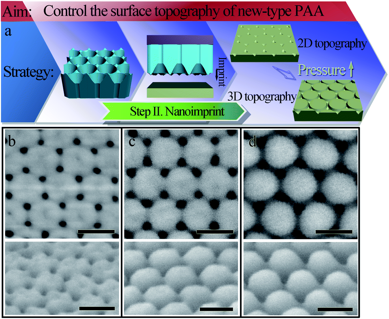 | ||
| Fig. 4 New-type PAA tuned using imprinting pressure in Step II. (a) Schematic of the surface topography of pre-patterned Al sheets tailored using imprinting pressure. Typical SEM top and side views of new-type PAA obtained by anodization of pre-patterned Al sheets under different imprinting pressures: (b) 0.15 GPa, (c) 0.25 GPa and (d) 0.35 GPa. The scale bar represents 100 nm. | ||
Apart from the observation that the new-type PAAs can be tuned by varying Vstamp and imprinting pressure, we also tailored VPAA in Step III to control the growth of nanopores as illustrated in Fig. 5. In contrast to the aforementioned PAA with graphite lattice nanopores, diverse complex new-type PAAs were obtained. The upper route (Fig. 5a–d, Vstamp = 40 V and imprinting pressure = 0.15 GPa) corresponds to the new-type PAA with a 2D surface topography tailored using VPAA. Fig. 5b and S5d† show the typical SEM image of the new-type PAA with a 2D surface topography after the anodization (VPAA = 10 V). The new-type PAA consists of larger nanopores with a graphite lattice at patterned locations and unordered smaller nanopores at unpatterned regions. Obviously, the formation of larger nanopores is guided by the previously introduced pre-pattern. Similar to some previous observations,23,25 the smaller nanopores originate from self-compensation properties of anodic porous alumina during the anodization (Fig. S5a†). Furthermore, we found that at the defined unimprinted locations of the Al, pores can be compensated automatically and ordered alternating diameter nanopore arrangements are obtained at an appropriate anode voltage (VPAA = 20 V, Fig. S5b†). Fig. 5a and S5e† show the typical SEM micrographs of the as-prepared new-type 2D PAA with ordered hexagonal pores with an average interpore distance of 51 nm. The interpore distance of the new-type PAA is 1/√3 of the interpore distance of the conventional PAA stamp. The technique shows great potential in enlarging the anodization window15 and is important for fabricating PAA with ultra-high density hexagonal pores. When VPAA increases to 40 V, a new-type PAA with approximately hexagonal induced pores and unformed shallow pores was obtained. The phenomenon is noticeably different from that of the conventional self-organized PAA and the known induced PAA discussed so far. It may again be understood based on the equifield strength controlled oxide layer growth model and field-enhanced oxide dissolution (Fig. S5c and g†).23,24 The result indicates that we can further control the site of guided nanopores by tuning VPAA to fabricate diverse pore arrangements. In addition, the lower route (Fig. 5e–h, Vstamp = 40 V and imprinting pressure = 0.35 GPa) corresponds to a new-type PAA with a 3D surface topography tuned using VPAA. New-type PAAs with 3D central nanoislands and surrounding nanopores are obtained. Compared with the nanopores in Fig. 5b and c, the nanopores in Fig. 5f and g are mainly distributed in the concave pre-pattern and there are almost no self-compensated pores on the central nanoislands at an early stage of pore growth. Similar behavior is rarely reported in the previous literature. We attribute this to the effective guidance of the concave pre-pattern and central convex nanoislands with opposite curvature (Fig. S6†).
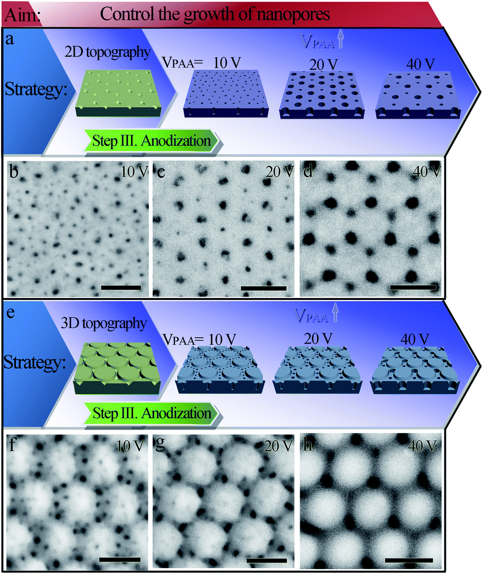 | ||
| Fig. 5 New-type PAA tuned using VPAA in Step III. The upper route corresponds to the new-type PAA with a 2D surface topography tuned using VPAA: (a) schematic diagram, typical SEM images of new-type PAA with VPAA of (b) 10 V, (c) 20 V and (d) 40 V, respectively. The lower route corresponds to the new-type PAA with a 3D surface topography tuned using VPAA: (e) schematic diagram, typical SEM images of a new-type PAA with a VPAA of (f) 10 V, (g) 20 V and (h) 40 V, respectively. The scale bar represents 100 nm. | ||
Conclusions
In summary, we have demonstrated the flexible fabrication of tunable new-type PAA membranes based on a simple and low-cost nanoimprint process. This technique has the potential to realize the tailoring of new-type PAAs with desired para-pore spacing, surface topography and nanopore arrangement, which are hard to obtain by the previous guided anodization, only using simple and cost-effective equipment, available to most researchers. The new-type PAAs as useful templates have many potential applications in designing and fabricating photonic, electronic and magnetic devices.Conflicts of interest
There are no conflicts to declare.Acknowledgements
This work was supported jointly by the Natural Science Foundation of the Jiangsu Higher Education Institutions of China, under Grant No. 18KJB430003, the China Postdoctoral Science Foundation Funded Project, under Grant No. 2020T130013ZX, the National Natural Science Foundation of China, under Grant No. 11874108 and 51501018, and the Natural Science Foundation of Jiangsu Province, China, under Grant No. BK20150267.References
- L. Zhou, Y. L. Tan, D. X. Ji, B. Zhu, P. Zhang, J. Xu, Q. Q. Gan, Z. F. Yu and J. Zhu, Sci. Adv., 2016, 2, e1501227 CrossRef PubMed.
- K. Swathi and K. S. Narayan, Nano Lett., 2017, 17, 7945–7950 CrossRef CAS PubMed.
- L. Y. Wen, R. Xu, Y. Mi and Y. Lei, Nat. Nanotechnol., 2017, 12, 244–250 CrossRef CAS PubMed.
- C. Y. Liu, E. I. Gillette, X. Y. Chen, A. J. Pearse, A. C. Kozen, M. A. Schroeder, K. E. Gregorczyk, S. B. Lee and G. W. Rubloff, Nat. Nanotechnol., 2014, 9, 1031–1039 CrossRef CAS PubMed.
- Q. L. Wei, Y. Q. Fu, G. X. Zhang, D. C. Yang, G. W. Meng and S. H. Sun, Nano Energy, 2019, 55, 234–259 CrossRef CAS.
- H. Masuda and K. Fukuda, Science, 1995, 268, 1466–1468 CrossRef CAS PubMed.
- H. Masuda, H. Asoh, M. Watanabe, K. Nishio, M. Nakao and T. Tamamura, Adv. Mater., 2001, 13, 189–192 CrossRef CAS.
- B. Chen, K. Lu and Z. P. Tian, Langmuir, 2011, 27, 800–808 CrossRef CAS PubMed.
- S. Lee, D. Kim, E. Gillette, J. Oh, S. W. Han and S. B. Lee, Phys. Chem. Chem. Phys., 2013, 15, 10659–10665 RSC.
- J. T. Smith, Q. Hang, A. D. Franklin, D. B. Janes and T. D. Sands, Appl. Phys. Lett., 2008, 93, 043108 CrossRef.
- T. Kondo, H. Miyazaki, T. Yanagishita and H. Masuda, Electrochem. Commun., 2018, 96, 61–65 CrossRef CAS.
- C. Y. Liu and S. Biring, Microporous Mesoporous Mater., 2019, 287, 71–76 CrossRef CAS.
- H. Masuda, H. Yamada, M. Satoh, H. Asoh, M. Nakao and T. Tamamura, Appl. Phys. Lett., 1997, 71, 2770–2772 CrossRef CAS.
- W. Lee, R. Ji, C. A. Ross, U. Gosele and K. Nielsch, Small, 2006, 2, 978–982 CrossRef CAS PubMed.
- T. S. Kustandi, W. W. Loh, H. Gao and H. Y. Low, ACS Nano, 2010, 4, 2561–2568 CrossRef CAS PubMed.
- S. Fournier-Bidoz, V. Kitaev, D. Routkevitch, I. Manners and G. A. Ozin, Adv. Mater., 2004, 16, 2193–2196 CrossRef CAS.
- X. N. Wang, S. P. Xu, M. Cong, H. B. Li, Y. J. Gu and W. Q. Xu, Small, 2012, 8, 972–976 CrossRef CAS PubMed.
- C. S. Li, J. Li, C. Chen, J. Zhu and X. F. Gao, Chem. Commun., 2012, 48, 5100–5102 RSC.
- C. Zhang, W. C. Li, D. L. Yu, Y. S. Wang, M. Yin, H. Wang, Y. Song, X. F. Zhu, P. C. Chang, X. Y. Chen and D. D. Li, Adv. Mater. Interfaces, 2017, 4, 1601116 CrossRef.
- X. Z. Lang, T. Qiu, K. L. Long, D. Han, H. Y. Nan and P. K. Chu, Nanotechnology, 2013, 24, 255303 CrossRef PubMed.
- X. Z. Lang, T. Qiu, W. J. Zhang, Y. Yin and P. K. Chu, J. Phys. Chem. C, 2011, 115, 24328–24333 CrossRef CAS.
- S. Kasani, K. Curtin and N. Q. Wu, Nanophotonics, 2019, 8, 2065–2089 CAS.
- J. Choi, R. B. Wehrspohn and U. Gosele, Electrochim. Acta, 2005, 50, 2591–2595 CrossRef CAS.
- Z. X. Su, G. Hahner and W. Z. Zhou, J. Mater. Chem., 2008, 18, 5787–5795 RSC.
- H. Masuda, M. Yotsuya, M. Asano, K. Nishio, M. Nakao, A. Yokoo and T. Tamamura, Appl. Phys. Lett., 2001, 78, 826–828 CrossRef CAS.
Footnote |
| † Electronic supplementary information (ESI) available. See DOI: 10.1039/d0na00916d |
| This journal is © The Royal Society of Chemistry 2021 |