
 Open Access Article
 This Open Access Article is licensed under a Creative Commons Attribution-Non Commercial 3.0 Unported Licence
Optical simulation of ultimate performance enhancement in ultrathin Si solar cells by semiconductor nanocrystal energy transfer sensitization†
Brandon
Yalin
a,
Andreas C.
Liapis
*b,
Matthew D.
Eisaman
c,
Dmytro
Nykypanchuk
b and
Chang-Yong
Nam
 *b
*b
aDepartment of Physics and Astronomy, Stony Brook University, Stony Brook, New York 11794, USA
bCenter for Functional Nanomaterials, Brookhaven National Laboratory, Upton, New York 11973, USA. E-mail: andreas.liapis@gmail.com; cynam@bnl.gov
cDepartment of Electrical and Computer Engineering, Stony Brook University, Stony Brook, New York 11794, USA
First published on 8th January 2021
Abstract
Energy transfer (ET) from nanocrystals (NCs) has shown potential to enhance the optoelectronic performance of ultrathin semiconductor devices such as ultrathin Si solar cells, but the experimental identification of optimal device geometries for maximizing the performance enhancement is highly challenging due to a large parameter space. Here, we have demonstrated a general theoretical framework combining transfer matrix method (TMM) simulations and energy transfer (ET) calculations to reveal critical device design guidelines for developing an efficient, NC-based ET sensitization of ultrathin Si solar cells, which are otherwise infeasible to identify experimentally. The results uncover that the ET-driven NC sensitization is highly effective in enhancing the short circuit current (JSC) in sub-100 nm-thick Si layers, where, for example, the ET contribution can account for over 60% of the maximum achievable JSC in 10 nm-thick ultrathin Si. The study also reveals the limitation of the ET approach, which becomes ineffective for Si active layers thicker than 5 μm, being dominated by conventional optical coupling. The demonstrated simulation approach not only enables the development of efficient ultrathin Si solar cells but also should be applicable to precisely assessing and analyzing diverse experimental device geometries and configurations for developing new efficient ET-based ultrathin semiconductor optoelectronic devices.
Introduction
With Si remaining the leading semiconductor material for photovoltaic devices, there has been a strong push towards maximizing efficiencies of thin-film Si solar cells in an effort to reduce module cost and material consumption. Efficiencies greater than 25% have been theorized for Si thicknesses in the 10–50 μm range.1 Si layers with thicknesses in the tens of micrometers can be reliably made with little to no kerf loss using, for instance, thermal expansion mismatch to mechanically exfoliate thin monocrystalline Si layers from a parent wafer. Such kerfless wafering techniques have been recently used to produce thin Si solar cells.2–7 An important open question however is the effectiveness of ultrathin, sub-μm Si solar cells. Thinner Si layers in general offer increased open circuit voltage in the Auger recombination limited regime, in addition to decreased surface and bulk recombination, however, all at the expense of limited light absorption.8 For such thin layers, optical techniques to ensure sufficient light absorption would be highly important for improving the device performance.9We have previously studied the applicability of semiconductor nanocrystal (NC) sensitizers and their effects on photovoltaic device performance of ultrathin Si solar cells by incorporating CdSe–ZnS core–shell NCs atop a 500 nm thick ultrathin Si device layer.10 The experiment revealed a unique dual functionality of the NCs: Not only did they improve the optical coupling of incident light into the active ultrathin Si layer by acting as an anti-reflective coating, but they also improved light harvesting via direct energy transfer (ET) from the NCs into the Si layer through radiative and nonradiative ET processes, consistent to what has been originally proposed and identified by the Malko group in a series of reports.11,12 A similar ET-based NC sensitization scheme has been recently used to improve the light absorption in a Si-based photodetector,13 organic–inorganic hybrid perovskites,14 and various two-dimensional semiconductors.15–19
For these devices including ultrathin Si solar cells, further enhancement of device performances by NC sensitization may be possible by optimizing the device design parameters. For ultrathin Si solar cells, the key parameters would be those related with the device layer stack geometries, such as the thicknesses of the NC, spacer, and active Si layers, which control both ET efficiency and conventional optical coupling of light throughout the device stack in a complex manner. However, a full experimental optimization of these parameters is not feasible practically due to a large parameter space, and the ultimate performance enhancement of ultrathin Si solar cells achievable by the ET-based NC sensitization remains unknown. The same challenge would apply to other optoelectronic device systems that try to utilize ET schemes for improving devices' optical absorption and associated performances.
In this work, we have demonstrated a simulation approach combining the transfer matrix method (TMM) and ET-based dipole calculations to provide a general theoretical framework that can survey an extensive range of the parameter space for the layer geometry of NC-sensitized ultrathin Si solar cells and, ultimately, to identify optimized device geometries that maximize the performance enhancement achievable by the NC sensitization approach. The accuracy of this calculation approach has been successfully tested previously by experimentally obtained photovoltaic device performance data that showed an excellent matching with simulation results for a set of tested 500 nm-thick Si device geometries.10 In this study, the refined simulation scheme systematically surveyed a vastly extended device geometry parameter space, uncovering that the ET-based NC sensitization is highly effective in improving the light absorption in sub-μm-thick Si, wherein the ET can contribute to over 60% of the total short circuit current (JSC) output of 10 nm-thick ultrathin Si while also revealing the limitation of ET approach for improving the light absorption in Si active layers thicker than 5 μm, wherein a straightforward, conventional anti-reflective coating is effective for improving the light absorption.
Results and discussion
The NC-sensitized ultrathin Si consists of three primary component layers, from top to the bottom, NC layer (consisting of multiple NC monolayers), AlOx spacer, and ultrathin Si (on a 1 μm SiO2/500 μm Si handling layer of a Si-on-insulator (SOI) substrate) as in our previous experimental study (Fig. 1a), ensuring the accuracy of the modeling approach.10 Here, the AlOx spacer provides a physical separation between the NC donor layer and the active Si layer to prevent the direct charge transfer. The thicknesses of these three key individual layers intricately affect the efficiencies of optical coupling of incident light to the active ultrathin Si and ET from NCs to Si. Hence the three thicknesses are explored as the primary device geometry parameters of interest in this study. On the device stack, the light is incident from the top, similarly to the interdigitated back contact Si solar cell structure.20 The NCs feature a 4.5 nm diameter CdSe/ZnS inner semiconductor core/shell with a ∼1.7 nm thick polymer ligand outer coating (i.e., the total diameter of an NC = ∼8 nm). The chosen inner semiconductor core/shell diameter leads to a strong absorption below 400 nm and an emission at 605 nm, ensuring a good spectral overlap with the absorption spectrum of Si and, thus, an efficient ET. Meanwhile, the 1.7 nm-thick polymer ligand coating prevents the inter-NC charge transfer. When NC solution is spin-coated onto the device, NCs self-assemble into a stack of monolayers (Fig. 1a). We describe the NC layer using experimentally determined values of the frequency-dependent refractive index, n(ω), and extinction coefficient, k(ω), measured directly over the entire solar spectrum. The strong interaction of NCs with light offers great capabilities of incident light energy to be transferred to the proximal Si active layer by ET, where the two primary mechanisms present are radiative ET (RET) and nonradiative ET (NRET). In NRET, the direct transfer of absorbed energy from a NC to Si occurs via near-field dipole–dipole interactions that can be thought of as direct excitation of electron–hole pairs in Si by the evanescent electric field of the NC's, whose interactions with other energy absorption processes in Si such as phonon excitation are minor due to being off-resonance. On the other hand, RET is based on the decay of the NC exciton into photonic guided modes that propagate within, and are absorbed by, the proximal Si active layer.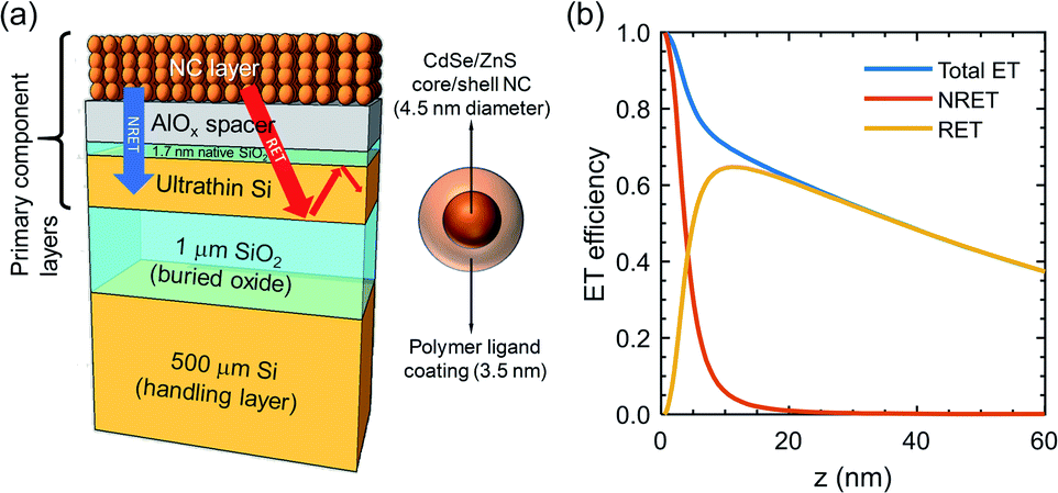 | ||
| Fig. 1 (a) NC-sensitized ultrathin Si structure modelled by TMM. (b) ET efficiencies for a single NC monolayer situated at a distance z above the layered dielectric system. | ||
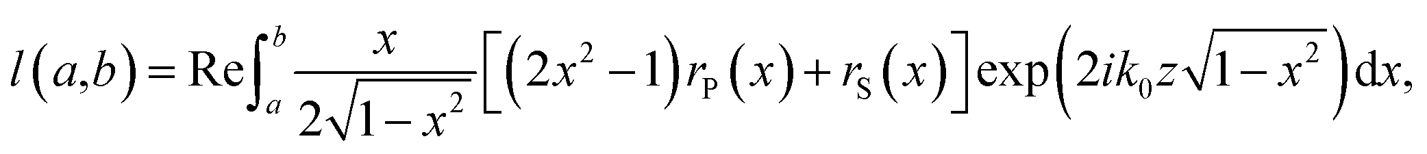
The efficiencies of NRET and RET are calculated by comparing the ratio of the decay rate, Γ, of a randomly oriented dipole at a distance z above a layered dielectric system to its vacuum decay rate Γo. In our calculations, each NC monolayer in a given thickness of NC layer is represented as being above the ultrathin Si layer at a height z spaced by a chosen thickness of AlOx plus 1.7 nm thick native SiO2 on Si, and the resulting total electromagnetic decay rate is given by:11
| Γ/Γo = 1 + l(0,∞), | (1) |
 | (2) |
| Γ = Γvac + ΓAlOx,SiO2 + ΓRET + ΓNRET, | (3) |
| Γvac/Γo = 1 + l(0,1), | (4) |
| ΓAlOx,SiO2/Γo = l(1,1.5), | (5) |
| ΓRET/Γo = l(1.5,nSi), | (6) |
| ΓNRET/Γo = l(nSi,∞). | (7) |
| ΓET = (ΓRET + ΓNRET)/Γ. | (8) |
Fig. 1b shows the dependence of NRET and RET to the distance between a single NC monolayer and the Si device layer. For distances greater than 5 nm, RET is the dominant factor contributing to the total ET efficiency. Notice that even at 120 nm separation, RET can allow the transfer of approximately 19% of the NC absorption. On the other hand, NRET quickly decreases (∝1/x3) and becomes negligible for distances greater than 20 nm.
To simulate the performance of NC-sensitized ultrathin Si solar cells, we employ the spatially resolved TMM which can describe the wave propagation through a sequence of homogenous media in one dimension. Specifically, the TMM is used to calculate the total light absorption within each device component layer in the device stack as a function of the layer depth for each wavelength. We note that each device component layer was treated as homogenous medium without intra-layer scattering. Particularly, for the NC sensitization layer of a given thickness that can contain multiple, stacked NC monolayers (each 8 nm thick; i.e., the diameter of a NC), this approximation is valid, considering that the inter-ET among individual NCs is less than 3.5%.10
In order to obtain the total energy that is transferred from the NC sensitization layer to the Si membrane via ET (AET), we summate the energy (light) absorbed by each NC monolayer (ANC) calculated by TMM, weighted by the average ET efficiency of the 8 nm interval given by eqn (8):
| AET = ∑(ANC × ΓET). | (9) |
Then, the sum of AET with the total light absorbed in the Si layer via pure optical coupling (ASi) yields the final, total energy absorbed by the Si layer, Atotal = AET + ASi, in the given combination of component layer thicknesses. Note that ASi is in general higher than the energy absorbed by an equivalent Si solar cell in the absence of a sensitization layer, as the NC layer improves light coupling into the Si by acting as an antireflective coating. The ultimate short circuit current density (JSC) then can be estimated by integrating the wavelength-dependent absorption over the standard 1 sun (i.e., 100 mW cm−2) solar spectrum under the air mass 1.5 global condition (EAM1.5G):
 | (10) |
Using the modeling approach discussed above, we first examine the dependence of JSC of an ultrathin Si solar cell with a 500 nm thick active Si layer on the thicknesses of NC sensitization layer and AlOx spacer (Fig. 2). In our simulations, the thickness of the AlOx spacer is varied from 0 to 120 nm in 2 nm steps, while the NC sensitization layer is varied from 0 to 15 NC monolayers (i.e., thickness range of 0–120 nm in 8 nm steps). The total JSC for the Si device layer is then broken down into the contributions from the two pathways: Joptical, originating from ASi in eqn (10), represents the current originating from light absorbed by the Si device layer and includes anti-reflective effects, and JET originates from light absorbed by the NC layer, whose energy is then transferred both radiatively and non-radiatively to the Si active layer, such that JSC = Joptical + JET. In addition, the relative percentage enhancement in JSC due to the inclusion of the NC and AlOx layers compared with a bare solar cell is calculated for context.
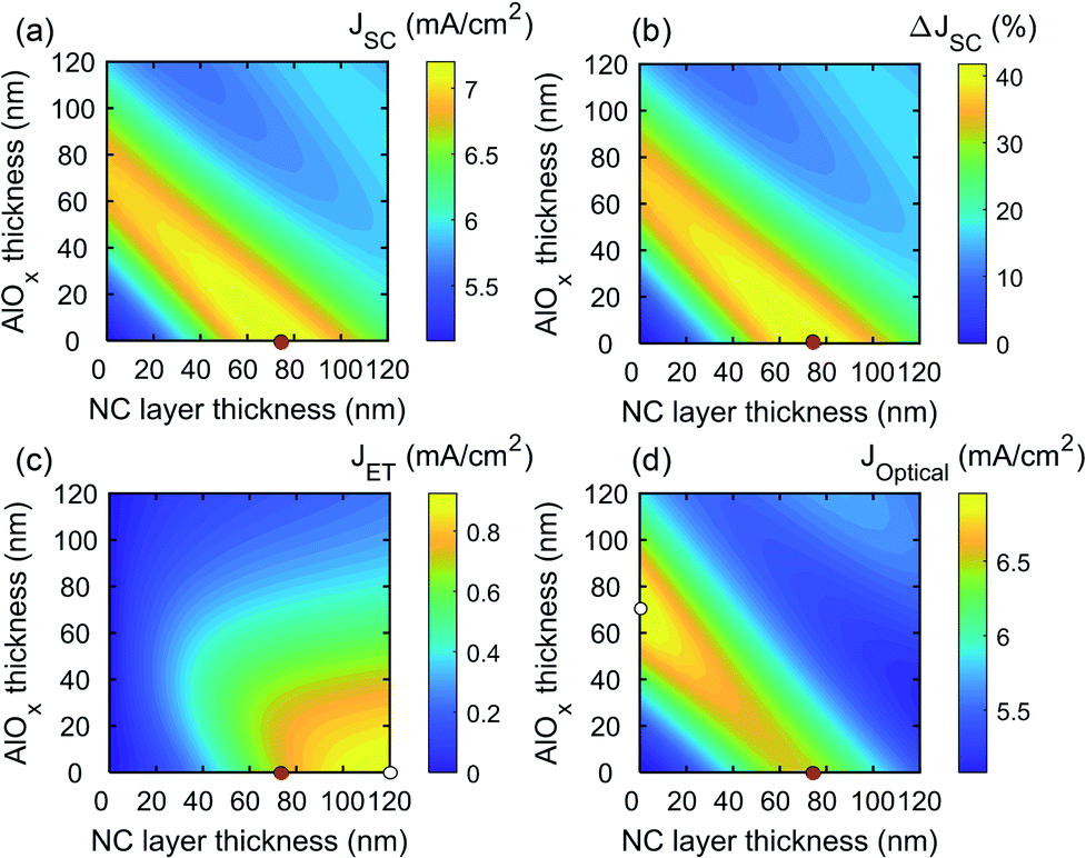 | ||
| Fig. 2 Contour plots depicting the calculated (a) JSC, (b) its relative enhancement compared to the case of zero AlOx thickness and zero NC layer thickness, as well as the individual contributions (c) JET, and (d) Joptical for a 500 nm thick ultrathin Si as functions of the thicknesses of NC sensitization layer and AlOx spacer. Red dots denote the configuration that yields the maximum JSC and the white dots in (c) and (d) the configurations for the maximum JET and Joptical, respectively. | ||
As shown Fig. 2a, the 500 nm thick ultrathin Si exhibits a maximum JSC of 7.255 mA cm−2 when using a 72 nm thick NC layer (9 NC monolayers) without AlOx spacer. The survey features a large band in the parameter space that is within 3% of the maximum JSC, indicating a wide latitude for optimal thicknesses of component layers for enhancing photovoltaic efficiency. The maximum JSC of 7.255 mA cm−2 amounts to a 42.79% relative enhancement compared with the 500 nm thick ultrathin Si without employing the NC sensitization layer (Fig. 2b). It is noted that JSC of 7.255 mA cm−2 would represent ∼3.1% power conversion efficiency (PCE) assuming open circuit voltage (VOC) of 0.56 V and fill factor (FF) of 0.76, which have been demonstrated in 500 nm-thick microcrystalline Si solar cells.9 Out of the maximum JSC of 7.255 mA cm−2, the contribution of JET is 0.705 mA cm−2 (Fig. 2c), constituting 9.7% of the total JSC. Meanwhile, the maximum JET occurs when a 120 nm thick NC layer (i.e., 15 NC monolayers) is used, yielding JET of 0.949 mA cm−2. The simulation results also show that the maximum Joptical is 7.002 mA cm−2 when using 70 nm of AlOx spacer without NC sensitization (Fig. 2d). The local region of the maximum Joptical is far more pronounced than that of the case of JSC, but a band of optimal thickness combinations is still present, extending from 70 nm AlOx without NC layer (i.e., coordinate of (0, 70) in Fig. 2d) to 72 nm thick NC layer without AlOx spacer ((72, 0) in Fig. 2d), where Joptical decreases to 6.551 mA cm−2. We note that the optical coupling to the NC layer and, thus, JET are not evenly distributed throughout all the NC layer thickness surveyed, as evident by the ‘bowing’ that the contours follow in Fig. 2c; for the 16–80 nm thick NC layer (2–10 NC monolayers), JET initially increases with increasing AlOx spacer thickness on the interval from 0 nm to 40 nm. Overall, considering both ET and optical coupling, the results demonstrate that the bifunctional properties of NC sensitization narrowly outcompetes the standalone AlOx-only coating for enhancing the photovoltaic performance of 500 nm thick ultrathin Si.
Applying the modeling framework implemented above, we can expand our survey to various Si thicknesses in order to study the evolution of JSC. Devices with Si thicknesses of 10 nm, 100 nm, 1 μm, 5 μm, 10 μm, 25 μm, 50 μm, and 100 μm were simulated, and the resulting calculated maximum JSC for each Si thickness is summarized in Fig. 3a. For 10 nm-thick ultrathin Si, ET provides the main contribution to JSC as indicated by the characteristic maximum achievable at 120 nm NC layer thickness (15 NC monolayers) with zero AlOx spacer thickness (Fig. 3b) as well as the similar bowing as seen in the JET contour for 500 nm thick Si layer (Fig. 2c), except for the broadened range of values originating from the minor Joptical contribution. Compared with the Si layer without NC sensitization, JSC has increased by over three-fold from 0.44 mA cm−2 to 1.31 mA cm−2 of which ET accounted for over 60% of the total JSC (JET ∼ 0.8 mA cm2; Fig. 3a). The results highlight that the NC sensitization is highly effective for ultrathin Si with sub-100 nm thickness, which otherwise exhibits a limited direct light absorption. For the 100 nm thick Si, the maximum JSC is now increased to 3.12 mA cm−2 (Fig. 3c) at 72 nm NC layer thickness (9 monolayers). The reduced optimal NC layer thickness for maximizing JSC compared with 10 nm thick Si indicates an increasingly dominating contribution of Joptical over JET which now constitutes only ∼25% of total JSC (JET ∼ 0.79 mA cm2; Fig. 3a). When the Si layer thickness is increased to 1 μm, the maximum JSC increases to 10.21 mA cm−2 (Fig. 3d) with the enhancement by NC sensitization nearly entirely driven by an improved optical coupling as ET contributes only ∼7.4% of the total JSC (JET ∼ 0.76 mA cm2; Fig. 3a). Due to the diminishing ET contribution, the application of standalone AlOx layer without NC layer results in nearly equivalent JSC, and the JSC contour plot features a large, extended yellow band in which the NC-sensitized 1 μm-thick Si maintains a near maximum JSC over various combinations of thicknesses of NC layer and AlOx spacer (Fig. 3d).
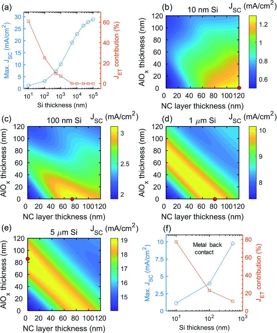 | ||
| Fig. 3 (a) Maximum JSC (blue circle) and JET contribution (red square) as a function of NC-sensitized Si layer thickness. Contour plots of calculated maximum JSC of NC-sensitized Si layers with different Si thicknesses: (b) 10 nm, (c) 100 nm, (d) 1 μm, and (e) 5 μm. Red dots denote the thickness configuration that yields the maximum JSC. (f) Maximum JSC (blue circle) and JET contribution (red square) as a function of NC-sensitized Si layer thickness with metal back contact of 100% reflectivity. | ||
For Si layers with thicknesses greater than 1 μm, the maximum JSC occurs when applying only AlOx spacer without NC sensitization layer and, thus, with no contribution from ET (Fig. 3a); as the Si layer thickness increases further from 5 μm to 100 μm, a standalone AlOx layer provides the greatest enhancement in JSC, reaching the maximum of 22.84 mA cm−2 for the 10 μm thick Si layer and 28.9 mA cm−2 for the 100 μm thick Si. If a NC layer is applied, JSC rather decreases as shown in Fig. 3e for the example of 5 μm-thick Si, which features an extended yellow band similar to 1 μm Si but now with the maximum being located at zero NC layer thickness.
We note that the overall JSC of the solar cell presented so far can be increased significantly if the bottom surface of Si active layer in the device structure utilizes better light management schemes, such as the reflective metallic back contact used in interdigitated back contact solar cells, instead of the SOI structure considered in the current study. We confirm the notion by extending the modeling to determine the maximum JSC and its JET contribution for the Si thicknesses of 10, 100, and 500 nm with a metallic back contact with unity reflectivity (without diffuse scattering); as shown in Fig. 3f (also Fig. S1 in ESI†), the results indeed show superior maximum JSC as well as enhanced JET contribution compared with the counterpart without the reflective back contact. For example, a 500 nm-thick Si with a metallic back contact can output ∼10 mA cm−2 as opposed to ∼7.3 mA cm−2 without the back contact discussed earlier. Furthermore, for the 10 nm-thick Si with a back contact, JET now contributes ∼80% to the maximum JSC, being improved from ∼60% contribution without a back contact.
Conclusions
In summary, we have performed an optical simulation survey combining the ET calculation and TMM modeling, confirming the efficacy of NC sensitization for improving the photovoltaic performance of ultrathin Si solar cells, which is enabled by an increased light absorption in the Si layer via direct ET and improved optical coupling. The approach is revealed to be particularly effective for enhancing the light absorption in sub-100 nm thick ultrathin Si layers because the dominant contribution from ET circumvents the intrinsically inferior optical coupling of incident light in such ultrathin Si layers, while less effective for Si thicknesses over 1 μm. The results from 10 nm-thick ultrathin Si layer well exemplify the notion, where the ET constituted over 60% of the maximum achievable JSC and even 80% if a reflective metallic back contact is adopted. It is noted that under the ideal case of light management known as Tiedje–Yablonovitch (TY) limit that assumes zero reflectivity at the front surface and a unity reflectivity with diffuse scattering at the bottom surface,21 the maximum JSC of ultrathin Si is expected to be much higher than what has been shown in the current study. However, the noted zero front-surface reflectivity and unity bottom-surface reflectivity/diffuse scattering required for the TY limit are nearly impossible to realize in ultrathin Si with sub-500 nm thickness because the known necessary light trapping schemes such as micro/nanotexturing have the length and depth scales ranging from 100s of nanometers22 to ∼10 μm,23 exceeding the ultrathin Si thickness. This again highlight the unique advantage of utilizing ET for improving the light absorption in ultrathin Si. Overall, our modeling results identified a range of device subcomponent layer thickness combinations optimal for maximizing JSC for a given thickness of ultrathin Si, providing useful design guidelines towards developing highly effective ET-enhanced ultrathin Si solar cells. Considering a weak light absorption is a common issue in many ultrathin materials such as two-dimensional van der Waals semiconductors,19 the general theoretical framework encompassing both TMM and ET calculations demonstrated in this study should find utility beyond ultrathin Si solar cells, providing precise assessment and analysis of diverse device geometries and configurations with large parameter spaces in advanced ET-based ultrathin semiconductor optoelectronic devices.Conflicts of interest
There are no conflicts to declare.Acknowledgements
This research was carried out at the Center for Functional Nanomaterials, which is a U.S. DOE Office of Science Facility, at Brookhaven National Laboratory under Contract No. DE-SC0012704.References
-
S. Bowden, presented in part at the 19th Workshop on Crystalline Silicon Solar Cell Materials and Processes, Breckenridge, CO, 2009 Search PubMed
.
- M. M. Hilali, S. Saha, E. Onyegam, R. Rao, L. Mathew and S. K. Banerjee, Appl. Opt., 2014, 53, 6140–6147 CrossRef
- E. U. Onyegam, D. Sarkar, M. M. Hilali, S. Saha, L. Mathew, R. A. Rao, R. S. Smith, D. Xu, D. Jawarani, R. Garcia, M. Ainom and S. K. Banerjee, Appl. Phys. Lett., 2014, 104, 153902 CrossRef
- H.-S. Lee, J. M. Choi, B. Jung, J. Kim, J. Song, D. S. Jeong, J.-K. Park, W. M. Kim, D.-K. Lee, T. S. Lee, W. S. Lee, K.-S. Lee, B.-K. Ju and I. Kim, Sci. Rep., 2019, 9, 19736 CrossRef CAS
- A. Kumar Dikshit, N. Chandra Mandal, S. Bose, N. Mukherjee and P. Chakrabarti, Sol. Energy, 2019, 193, 293–302 CrossRef CAS
- C. Yang, K. Moon, J.-W. Song, J. Kim, J.-H. Lee, J.-H. Lim and B. Yoo, J. Electrochem. Soc., 2018, 165, D243–D249 CrossRef CAS
- I. Hwang, H.-D. Um, B.-S. Kim, M. Wober and K. Seo, Energy Environ. Sci., 2018, 11, 641–647 RSC
- M. J. Kerr, A. Cuevas and P. Campbell, Prog. Photovoltaics, 2003, 11, 97–104 CAS
- M. De Zoysa, K. Ishizaki, Y. Tanaka, H. Sai, K. Matsubara and S. Noda, Appl. Phys. Express, 2016, 10, 012302 CrossRef
- S. Hoang, A. Ashraf, M. D. Eisaman, D. Nykypanchuk and C.-Y. Nam, Nanoscale, 2016, 8, 5873–5883 RSC
- H. M. Nguyen, O. Seitz, W. Peng, Y. N. Gartstein, Y. J. Chabal and A. V. Malko, ACS Nano, 2012, 6, 5574–5582 CrossRef CAS
- M. T. Nimmo, L. M. Caillard, W. De Benedetti, H. M. Nguyen, O. Seitz, Y. N. Gartstein, Y. J. Chabal and A. V. Malko, ACS Nano, 2013, 7, 3236–3245 CrossRef CAS
- W. Peng, S. Sampat, S. M. Rupich, B. Anand, H. M. Nguyen, D. Taylor, B. E. Beardon, Y. N. Gartstein, Y. J. Chabal and A. V. Malko, Nanoscale, 2015, 7, 8524–8530 RSC
- Y. Cabrera, S. M. Rupich, R. Shaw, B. Anand, M. de Anda Villa, R. Rahman, A. Dangerfield, Y. N. Gartstein, A. V. Malko and Y. J. Chabal, Nanoscale, 2017, 9, 8695–8702 RSC
- T. Guo, S. Sampat, K. Zhang, J. A. Robinson, S. M. Rupich, Y. J. Chabal, Y. N. Gartstein and A. V. Malko, Sci. Rep., 2017, 7, 41967 CrossRef CAS
- Y. Huang, H. Zang, J.-S. Chen, E. A. Sutter, P. W. Sutter, C.-Y. Nam and M. Cotlet, Appl. Phys. Lett., 2016, 108, 123502 CrossRef
- M. Li, J.-S. Chen, P. K. Routh, P. Zahl, C.-Y. Nam and M. Cotlet, Adv. Funct. Mater., 2018, 28, 1707558 CrossRef
- M. Li, J.-S. Chen and M. Cotlet, ACS Photonics, 2019, 6, 1451–1457 CrossRef CAS
- M. Li, J.-S. Chen and M. Cotlet, ACS Energy Lett., 2019, 4, 2323–2335 CrossRef CAS
- P. J. Verlinden, R. M. Swanson and R. A. Crane, Prog. Photovoltaics, 1994, 2, 143–152 CAS
- T. Tiedje, E. Yablonovitch, G. D. Cody and B. G. Brooks, IEEE Trans. Electron Devices, 1984, 31, 711–716 Search PubMed
- A. Rahman, A. Ashraf, H. Xin, X. Tong, P. Sutter, M. D. Eisaman and C. T. Black, Nat. Commun., 2015, 6, 5963 CrossRef CAS
- P. Campbell and M. A. Green, Sol. Energy Mater. Sol. Cells, 2001, 65, 369–375 CrossRef CAS
Footnote |
| † Electronic supplementary information (ESI) available: Calculated contour plots of JSC and contributions of Joptical and JET for NC-sensitized ultrathin Si with metallic back contact with 100% reflectivity for Si thicknesses of: 10 nm; 100 nm, and 500 nm. See DOI: 10.1039/d0na00835d |
| This journal is © The Royal Society of Chemistry 2021 |