
 Open Access Article
 This Open Access Article is licensed under a Creative Commons Attribution-Non Commercial 3.0 Unported Licence
Critical challenges and advances in the carbon nanotube–metal interface for next-generation electronics
Farhad
Daneshvar
 ab,
Hengxi
Chen
b,
Kwanghae
Noh
b and
Hung-Jue
Sue
*b
ab,
Hengxi
Chen
b,
Kwanghae
Noh
b and
Hung-Jue
Sue
*b
aIntel Ronler Acres Campus, Intel Corp., 2501 NE Century Blvd, Hillsboro, Oregon 97124, USA
bPolymer Technology Centre, Department of Materials Science and Engineering, Texas A&M University, College Station, Texas 77843, USA. E-mail: hjsue@tamu.edu
First published on 6th January 2021
Abstract
Next-generation electronics can no longer solely rely on conventional materials; miniaturization of portable electronics is pushing Si-based semiconductors and metallic conductors to their operational limits, flexible displays will make common conductive metal oxide materials obsolete, and weight reduction requirement in the aerospace industry demands scientists to seek reliable low-density conductors. Excellent electrical and mechanical properties, coupled with low density, make carbon nanotubes (CNTs) attractive candidates for future electronics. However, translating these remarkable properties into commercial macroscale applications has been disappointing. To fully realize their great potential, CNTs need to be seamlessly incorporated into metallic structures or have to synergistically work alongside them which is still challenging. Here, we review the major challenges in CNT–metal systems that impede their application in electronic devices and highlight significant breakthroughs. A few key applications that can capitalize on CNT–metal structures are also discussed. We specifically focus on the interfacial interaction and materials science aspects of CNT–metal structures.
 Farhad Daneshvar | Dr Farhad Daneshvar obtained his PhD in Materials Science and Engineering from Texas A&M University in 2020. His research pertained to designing the interface of nanomaterials for high performance polymer and metal-based nanocomposites and hybrids. Prior to joining Dr Sue's research group at Texas A&M University, he was a Graduate Research Assistant at the Illinois Institute of Technology working on electrochemical energy storage systems. Currently, Farhad is a Technology Development Engineer at Intel Corporation. |
 Hengxi Chen | Hengxi Chen is a Research Assistant in the Polymer Technology Center of the Department of Materials Science and Engineering at Texas A&M University. He received his master's degree in Materials Engineering from the Viterbi School of Engineering, University of Southern California, in 2019. Prior to joining the USC in 2017, he earned his bachelor's degree in Polymer Science and Engineering from Donghua University in Shanghai. His research focuses on designing the interface between copper and carbon nanotubes in composite fibers, electrospun copper–carbon nanotube composite nanofibers, and fabrication of carbon nanotube/polymer nanocomposites. |
 Kwanghae Noh | KwangHae Noh is a PhD student in the Department of Materials Science and Engineering at Texas A&M University, College Station. He received his bachelor's degree in chemical engineering from Hanyang University, South Korea, in 2015. Currently, he is researching the fracture and scratch behavior of polymer nanocomposites at the Polymer Technology Center, Texas A&M, under the supervision of Prof. Hung-Jue Sue. |
 Hung-Jue Sue | Dr H.-J. Sue joined Texas A&M University in 1995 and holds M. H. Kotzebue ‘14 Professorship at the Materials Science and Engineering Department. He received his PhD degree from the University of Michigan in 1988 and was employed by Dow Chemical for 7 years. He has published over 300 journal articles and book chapters. He has trained over 80 PhD students and postdocs. His research interests include (1) nanomaterial synthesis and assembly for nanotechnology applications, (2) mechanical properties of polymers, and (3) scratch behavior of polymers. He is a fellow of the Society of Plastics Engineers. |
1 Introduction
Advanced electronic devices have become an essential part of human activities, from smart phones in our hands, to the modern vehicles on the streets, and to the satellites in space. The electronics industry is extremely fast-paced, striving for new discoveries and technologies. Every year a new generation of devices are produced which are faster, smaller, more energy efficient, more durable, and in some cases even cheaper than the older versions. It is expected that this industry will continue to be the driving force of major scientific and technological breakthroughs, leading to more powerful microprocessors, stretchable electronic skin, cheaper space exploration, and long-range electric vehicles. Development and discoveries of new materials are critical for advances and growth in the electronics industry.One of the materials with a promising future in electronics is carbon nanotubes (CNTs). CNTs are hollow quantum wires with extremely narrow diameters in the range of several atomic distances. They are basically rolled-up graphene sheets; hence, they share many similar chemical and physical properties. If the CNTs are composed of a single graphene layer, they are known as single-walled carbon nanotubes (SWCNTs), and if multiple concentric SWCNTs are arranged, they are classified as multi-walled carbon nanotubes (MWCNTs). Depending on the diameter and chiral angles, SWCNTs can exhibit metallic or semiconducting behavior. In metallic SWCNTs (m-SWCNTs) the band gap between valence and conduction bands is zero, while in semiconducting SWCNTs (s-SWCNTs) there is an energy gap. MWCNTs are generally considered as metallic.
In metallic CNTs the charge carriers are free to travel only along the axial directions and may show ballistic electron transport, i.e. without scattering, as confirmed experimentally.1 A m-SWCNT can have a maximum conductance of G = 4e2/h ≈ 0.15 m S (where h is the Planck constant).2 Experimental data have shown resistivity close to its theoretical value at 7.7 × 10⁻⁷ Ω cm−1. The lowest resistivity reported for a MWCNT is 5 × 10⁻⁶ Ω cm−1, which is lower than that of a SWCNT, probably due to the fact that MWCNTs have higher diameters than typical SWCNTs.3 Diffusive transport will be observed if the length of CNTs is larger than the ballistic regime. Ballistic transport may also be inhibited due to the increase in temperature or high electric fields. Nevertheless, individual SWCNTs at room temperature have exhibited a maximum current density of up to 1010 A cm−2 which is higher than even the critical current density of superconductors.4
Apart from the favorable electrical properties, CNTs possess excellent mechanical properties. The experimentally measured values of tensile modulus are approximately 0.3–0.95 TPa, tensile strength is approximately 10–100 GPa, and tensile strain is approximately 6–12%.5 The densities of SWCNTs and MWCNTs are about 1.3 g cm−3 and 2.1 g cm−3, respectively, which are significantly lower than those of typical electrical conductors, i.e. copper (8.96 g cm−3) and aluminum (2.7 g cm−3).
CNTs are excellent thermal conductors in the axial direction, with thermal conductivity exceeding that of the best-known bulk heat conductors, including diamond. Thermal conductivities in the axial direction of isolated SWCNTs and MWCNTs are experimentally determined to be 3500 and 3000 W m−1 K−1, respectively.6 Effective heat removal is much more efficient due to the high thermal conductivity and extremely high surface area of CNTs.7,8 Due to their low density, nanotubes have very high specific mechanical properties (strength or stiffness divided by density), which far exceed those of steel and other high-performance materials. These properties are highly important for their use as electrical conductors and may potentially help them to substitute metals in many applications.
Research into translating these highly attractive properties of CNTs from the nanoscale to the macroscale has, however, not been advancing smoothly. Attempts to fabricate macrostructures such as sheets and yarns have shown some promising results. For example, Tsentalovich et al. employed a wet-spinning process and produced CNT yarns, for achieving specific conductivity close to that of copper (Fig. 1).9 Even though this approach holds promise, the prohibitively expensive and laborious synthesis of CNTs on an industrial scale and lower conductivity hamper the applicability of this approach.
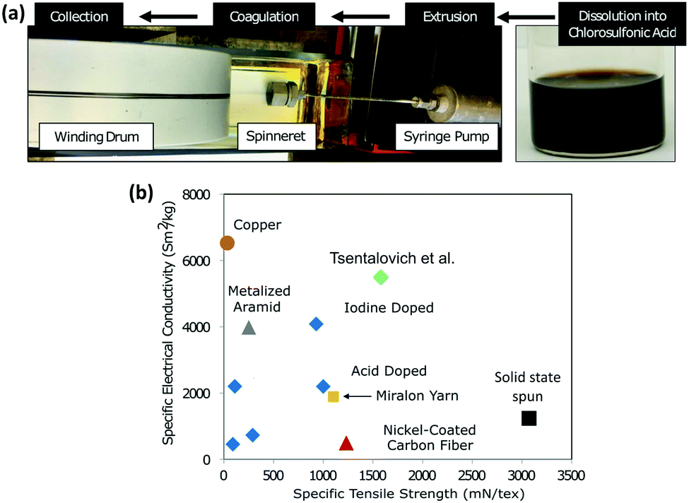 | ||
| Fig. 1 Specific electrical conductivity versus strength of CNT fibers produced by Tsentalovich et al. compared to that of previous fibers produced via superacid treatment (blue diamonds) and solid-state spinning (black square) and other conductive wires. Reproduced with permission from ref. 9. Copyright 2017, American Chemical Society. | ||
A different approach is to employ CNTs as nanofillers in copper matrices. The root of interest in carbon nanotube–metal composites for electrical conductors can be traced to a paper by Hjortstam et al., in which a theoretical approach was used to evaluate the possibility of fabricating an ultra-low resistivity carbon nanotube–metal composite. The simple effective-medium model predicts that at a 30–40 vol% filling factor, SWCNT–metal composites could present room temperature electrical conductivities approximately twice that of annealed copper.10 The combination of electrical, thermal, and mechanical property enhancements that CNTs offer when incorporated in a metal matrix leads to tremendous potential for these materials to serve as electrical cable conductors.
Several challenges have to be overcome before seeing the widespread adoption of CNT–metal structures. For instance, the length and quality of CNTs, CNT alignment and dispersion in a metal matrix, their interfacial contact, and manufacturing cost and scalability all need to be addressed. Also, it is necessary to ensure that the applied fabrication process does not compromise the chemical and structural stability of the CNTs. In this review, first, the main technological challenges ahead of CNT incorporation alongside metals in the electronic industry will be discussed. Throughout this review, special attention is placed on the interfacial interactions and materials science aspect of these challenges. These challenges include impurities, sorting, interface, and dispersion of CNTs. Subsequently, the latest breakthroughs in several applications for CNT–metal structures are reviewed. It is worth noting that although the focus of this work is on CNTs, many of the concepts discussed here are also applicable to graphene which shares many similar characteristics.
2 Challenges
There are several major technical challenges that impede widespread application of CNTs in future electronics. Some of these challenges are more application specific, for instance, the controlled synthesis and placement of CNTs is a main challenge in transistor applications,11–13 while for bulk composites, a uniform dispersion is the main issue. On the other hand, poor interfacial interaction between metals and CNTs is a more universal problem and is detrimental to many applications.2.1 Impurities
Regardless of the synthesis method, the as-produced CNTs contain impurities that can be classified into metallic and carbonaceous. Fe, Ni, Co, and Mo are the common metallic impurities which originate from the catalysts used in their synthesis process. The simplest way to determine the metal content of CNTs is performing a thermogravimetric analysis (TGA). Carbonaceous impurities, mainly amorphous and nanographitic carbon, are on the other hand more difficult to detect due to their similar composition to CNTs. Impurities can have detrimental effects on the properties and even toxicity of CNTs and their composites.14,15 For example, metallic impurities can dominate the magnetic properties16 and cause rapid decay in Li-ion batteries or electrochemical supercapacitors.17 Carbonaceous impurities also deteriorate the electrical, thermal, and mechanical properties of CNTs.18 Moreover, research has come to light that the initial claims regarding the outstanding electrochemical performance of CNTs with applications in sensors and energy storage are influenced by CNT impurities.19–21 Therefore, various processes are developed and implemented to remove the impurities.Acid treatment using a mixture of nitric and sulfuric acids is the most common practice for removing metallic impurities. However, this method can create defects, shorten the CNT length, and alter the surface chemistry of CNTs by creating surface groups especially when it is coupled with ultrasonication and high temperature treatments. Moreover, the catalyst residues that are commonly covered with amorphous carbon cannot be removed by this technique. Most of the undesirable surface groups can be removed by a subsequent annealing.22
Alternatively, it has been shown that the use of a mixture of H2O2 and a non-oxidizing acid such as HCl combined with ultrasonication and high temperature treatments is an effective way of removal of amorphous carbon and dissolving the catalyst residues without changing the surface chemistry of CNTs.22,23 Gas-phase oxidative processes such as annealing in air and/or O2,24 CO2,25 Cl2/O2 mixture,26 and steam27 can also be implemented to selectively remove carbonaceous impurities due to their lower stability than the CNT structure. However, this process should be done with care as defects and inorganic residues can decrease the decomposition temperature of CNTs.28 Heat treatment in a reducing atmosphere such as H2 and NH3 is also an effective approach for removing amorphous carbon. In this case, the carbonaceous impurities react with H2 and produce CH4 (while in an oxidizing atmosphere the product is CO).29
Finally, high purity and defect-free samples can be obtained through heat treatment in a vacuum or inert gases at high temperatures (>1600 °C). The carbonaceous impurities start to evaporate at around 600 °C while the metallic residues are removed at temperatures above 1600 °C. At around 2000 °C the carbon atoms in CNTs start to rearrange, reducing the number of structural defects. However, this process consumes a lot of energy and has low sample yield. Further details on this topic can be found in several review studies that have specifically focused on CNT purification.24,29,30
2.2 Separation and sorting
One of the main challenges for exploiting the properties of CNTs is their dispersity, meaning that in a batch CNTs with a wide range of sizes, chirality, and types exist. Even though most of the applications do not require selective CNT structures, some emerging applications, such as transistors or photothermal therapy, demand CNTs with specific architectures and/or properties.31 This is especially the case for SWCNTs, where they can be metallic or semiconducting in nature based on their chirality and diameter. Considering all being metallic, the research on sorting of MWCNTs is currently less attractive and is mainly limited to sorting based on their size.32,33 Therefore, this section will focus on separation and sorting of SWCNTs.SWCNT sorting begins with selective growth at synthesis. The catalyst used acts as a template for nucleation; hence, its crystal structure, shape, and morphology determine the SWCNT architecture.34,35 In high-temperature synthesis methods the catalyst microstructure at the interface can become unstable, which leads to loss of control over the SWCNT architecture. As a result, different strategies have been proposed to stabilize the catalyst interface including temperature adjustments during synthesis,36 tuning the catalyst–substrate interactions,37 controlling the atmosphere composition,34 and using intermetallic and inorganic oxide catalysts with high melting points, such as W–Co, Mo2C, WC, Al2O3 and TiO2.38,39 Another promising approach is using pre-sorted SWCNT segments which act as seeds for growth of a specific chirality.40–44 The growing CNTs preserve the structure of their seeds, which leads to products with high architecture uniformity. However, this method has low yield and is not economically viable.
A complementing strategy is to sort the SWCNTs after synthesis. The most common practice is based on using chemicals that selectively react with a specific type of SWCNT, thereby changing its dispersion or mobility in a solution. Consequently, conventional techniques such as filtration, centrifugation, and chromatography can be used for separating SWCNTs. For instance, diazonium salts tend to bond with metallic SWCNTs which changes their mobility and facilitates their separation through electrophoresis.45 It has been shown that surfactant sodium dodecyl sulfate (SDS) reduces the SWCNT interactions with sephacryl or allyl dextran-based gels, and also it has a higher affinity towards metallic SWCNTs and readily wraps around them. Therefore, by passing the CNT mixture through the gel, the semiconductor SWCNTs are gradually trapped, while metallic SWCNTs can be collected.46–48 Although this process (known as chromatography) is highly selective and efficient, it is complex, time consuming and is more suitable for short SWCNTs.24,46,49
DNA-assisted sorting is another attractive option since its sequence can be engineered to enhance its interaction towards a specific type of SWCNT.50 Similarly, various other polymers and copolymers have been designed to selectively interact with specific SWCNTs. For example, Tetronic with hydrophilic blocks favors metallic SWCNTs while pluronic that has short hydrophobic chains shows high affinity towards semiconductor SWCNTs.51 Polyfluorene family,52 polymethacrylate,49 carbazole-based polymers,53 and polythiophenes54 are among other polymers that have shown promising results. However, these polymer-based systems suffer from high material cost, leaving residues, and loss of polymers. Therefore, recent studies are focusing on developing polymers that can be easily removed and recovered to make the process more cost effective.52,55
In addition to the chemical techniques mentioned above, dielectrophoresis provides an effective approach for obtaining metallic SWCNTs. In this method, AC current creates a dipole on SWCNTs, depositing the metallic ones on the electrodes while the semiconductor SWCNTs remain in the solution.56,57 In a dry approach, SWCNTs can be exposed to high currents, leading to breakdown and removal of metallic SWCNTs while semiconductor ones remain intact.58 Overall, with recent advances in the sorting field, high selectivity (>99.99%) and high yield (>20%) have been achieved.13,55,59 However, for commercial applications, the scalability, efficiency, and cost of the processes still need to be further improved.
2.3 Interface
Due to the low affinity of CNTs for metals, controlling the interface remains a major technical challenge for metal–CNT structures. The side walls of defect-free CNTs are chemically inert which hinders the formation of strong bonds with metals. Moreover, metals are unable to wet the surface of CNTs mainly due to the significant difference in their surface energies (for instance, compare the 1800 mJ m−2 for Cu with the 27 to 45 mJ m−2 for CNTs).60,61 As a result, the properties of the CNT–metal systems, specifically the mechanical and electrical properties, are much lower than the theoretical predictions. It is well-known that for superior mechanical properties, strong covalent bonds between CNTs and metals are desired in order to enhance the load transfer.Definition of a “proper bond” in terms of electrical properties is more complex and some discrepancies exist in the literature. It is generally believed that strong covalent bonds are not conductive, and they can disrupt the electronic structure of CNTs.62 On the other hand, poor interfacial interaction also causes electron scattering at the interface. Another factor that adds to this complexity is the anisotropy in the structure of CNTs. Unlike side-walls, CNT ends have dangling bonds that can form covalent bonds with metals while junctions at the side-walls are assumed to be dominated by weak van der Waals forces. As a result, two types of interfacial geometries exist at CNT–metal junctions, end-contact and side-contact and they can form Schottky or ohmic contacts which have contrasting electronic properties (Fig. 2).63 It is worth adding that different metals interact very differently with CNTs even if they have similar types of bonding. In this section, the main focus will be on the electrical properties of CNT–metal junctions which are not as straightforward as the mechanical properties.
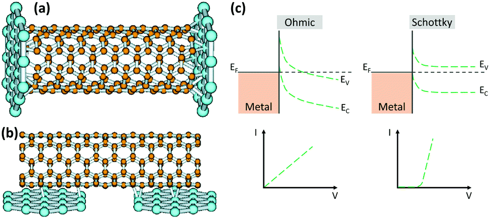 | ||
| Fig. 2 End-contact (a) and side-contact (b) geometries between metals and CNTs. Reprinted with permission from ref. 63. Copyright 2003, American Physical Society. Band diagrams for ohmic and Schottky junctions with the corresponding current–voltage plots (c). | ||
Carbon atoms in a CNT are tightly held together in a hexagonal pattern through strong σ bonds. Breaking these sp2-bonds requires a significant amount of energy, much higher than carbon–metal binding energies. Normal to these sp2-hybridized atoms, π-orbitals of carbon extend which can weakly bond with neighboring metals through hybridization between the carbon π-orbitals and the high energy orbitals of the metals. In the case of transition metals, these would be the outermost d-band orbitals. Among transition metals, the ones with more vacant d orbitals show more affinity towards CNTs.62 For example, in the periodic table group four, elements such as Ti or Fe that have more vacant 3d orbitals have stronger interactions than Cu which has a fully occupied 3d orbital. It should be noted that this rule is not specific to interactions with CNTs. In fact, surfaces of transition metals with few outer d-electrons react more easily with other elements such as oxygen. Depending on the metal and CNT curvature, it is assumed that side-contacts have physisorption or very weak chemisorption nature. For alkali and alkaline-earth metals (Al, Mg, etc.) where conduction is achieved through donation of sp-shells, the binding energy is around 1.5 eV. In transition metals with vacant d orbitals such as Ti and Ni, binding energy can reach around 2 eV per atom while for transition metals with fully occupied d orbitals the binding energies of side-contacts are below 1 eV per atom.64–66
The quality or strength of a side-contact of CNTs with a metal is largely influenced by wettability and binding energy of the metal. Metals such as Ti, Ni, and Pd that have high binding energy with CNTs can effectively wet their surface and show better interfacial interactions. It has been shown that these metals can form a continuous coating on CNTs while metals with poor wettability such as Au, Al, Cu, and Fe form discrete deposits on CNTs (Fig. 3a–f).67,68 The former is an indication of Frank–van der Merwe and the latter represents Volmer–Weber growth mechanisms. In the Frank–van der Merwe mode, adatoms of metals that have higher wettability for CNTs prefer to reduce the interfacial energy by attaching to the CNT surface and avoid forming islands which leads to uniform metal layers (Fig. 3g). On the other hand, a discrete growth mode occurs when the interfacial energy is relatively high and metal adatom–adatom interaction is stronger than the metal–substrate interaction. In the kinetics perspective, the mobility of the metallic adatoms on the CNT surface is lower than the rate of formation of new nuclei (Fig. 3h). These mechanisms are applicable for both gas-phase (such as sputtering) and liquid-phase (such as plating) deposition methods.
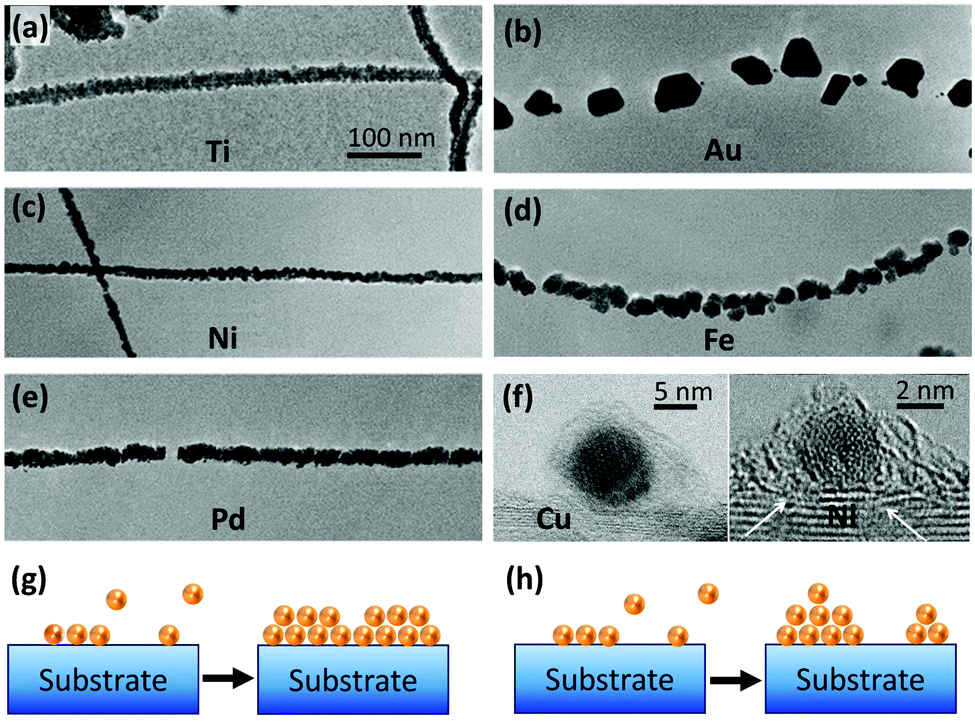 | ||
| Fig. 3 Transmission Electron Microscopy (TEM) images of (a) Ti, (b) Au, (c) Ni, (d) Fe, and (e) Pd coatings on CNTs. Reprinted with permission from ref. 67. Copyright 2000, Elsevier. (f) Comparison of Cu and Ni interaction with CNTs. The distance between Cu and CNTs is 4.1 Å, while for Ni it is 3.5 Å. The white arrows show a few Ni atoms diffused into the CNT structure. Reprinted with permission from ref. 68. Copyright 2015, Elsevier. Schematic of (g) Frank–van der Merwe and (h) Volmer–Weber growth mechanisms. | ||
The cohesive energy of a metal also has a major effect on how it interacts with CNTs. For example, in group eight where metals have the same number of d-valence electrons, under high energy irradiation Os, which has high cohesive energy, forms stable clusters, possibly forming σ bonds with SWCNTs. However, Fe which has high solubility for carbon readily forms carbides, and Ru stays metallic and has comparatively weaker bonds with CNTs. It is worth noting that σ bonds conduct electricity through quantum tunneling. Thus, they show higher contact resistance than the localized π bonds.66 Jang et al. used density functional theory (DFT) calculations to study the side-contacts of group 13 metals (Al, Ga, and In) with CNTs.64 In contrast to transition metals, d-orbitals are absent at the Fermi level of group 13 metals, and the valence electronic configuration is made of ns2np1 (n = 3, 4, 5) electrons. These metals show similar weak physisorption interactions with CNTs and do not alter the CNTs' electronic structure. This is attributed to the lack of d-orbitals, large equilibrium distance (exceeding 3 Å), and deficiencies in electron charge density at the interface.
End-contacts can be achieved when CNT open ends are embedded in or directly connected to the metal, leading to covalent bonding with stronger CNT–metal interaction compared with side-contacts.69–71 This type of contact geometry is commonly formed during CVD synthesis of CNTs, at their interface with the catalyst. At the CNT ends, carbon atoms are not bonded with three other carbon atoms which leaves dangling (or unsatisfied) bonds. These sp3-hybridized carbon atoms at CNT ends are able to form strong covalent bonds with metals. The covalent nature of these end-contact bonds has been shown by modelling and experimental studies.72–74 Accordingly, these bonds have significant mismatch-induced strains and show high tensile strength. Similar to side-contacts, metals with more vacant d orbitals form stronger end-contacts.
DFT calculations have shown that the binding energy of a covalent end-contact between Co and a CNT can reach 7.6 eV, much higher than that of typical side-contacts.73 Moreover, metals are able to form non-disruptive strong end-contacts with CNTs through carbide formation.75 It should be noted that in the vicinity of defects, metals can form localized σ bonds or covalent bonds similar to end-contacts which have higher bonding energy.28,66,76 A simple defect, such as a vacant carbon atom, can drastically alter the nature of CNT–metal bonding.
The electronic properties of CNT–metal junctions have been thoroughly studied in recent years. It is known that the junction between a conventional semiconductor and a metal has either Schottky or ohmic behavior (Fig. 2c). An ohmic junction is a low resistance contact in which current is linearly proportional to the applied voltage. In contrast, for a Schottky junction, an energy barrier forms at the interface and electrons need to overcome the barrier to be able to travel across the junction. Therefore, the resistivity decreases with increasing the temperature in Schottky contacts since at higher temperatures electrons have more mobility and can overcome the barrier. This is in contrast to ohmic contacts where the resistance linearly increases with increasing temperature. Unlike conventional semiconductor metal junctions, SWCNT–metal junctions are very small, just a few nanometers. Therefore, electrons can hop or tunnel through the barrier. As a result, the contact resistance in this case can be lower than for conventional semiconductor–metal Schottky junctions, but it is still higher than for an ohmic junction.
The electronic characteristics of metal–CNT junctions depend on whether the CNT is metallic or a semiconductor. Metallic CNTs often form ohmic contacts with metals regardless of the contact geometry. The contact resistance is mainly determined by the wettability of the metal and the degree of orbital hybridization around the junction.77 In terms of electronic properties, best contacts are achieved when the metal has enough binding energy to efficiently wet the CNT's surface but not too strong to damage its electronic properties.78 This explains why Ti which has very strong binding energy with CNTs is unable to form low contact resistance junctions. Experimental and theoretical studies have shown that Pd which has moderate binding energy and good wettability is able to form optimal electronic contacts with metallic CNTs.79–83
In light of potential applications of semiconductor CNTs in transistors, most of the research has focused on electronic properties of metal–semiconductor CNT junctions. These junctions can have either Schottky or ohmic behavior primarily depending on the metal's work function. Ohmic contacts are often desired due to their low contact resistance but they are difficult to achieve. Metals with a work function in the valence band of semiconducting CNTs can theoretically produce ohmic contacts (Fig. 2c). Accordingly, Pd with a work function of around 5.2 eV is able to form ohmic or low resistance Schottky junctions for both side- and end-contacts.81,84–86 It should be added that although the metal's work function is a prerequisite for ohmic contacts, other factors such as binding energy, contact type, and cohesive energy of the metal can also affect the quality of the contact. For example, Pt has similar work function and bonding characteristics to Pd but due to its comparatively high cohesive energy and poor wettability, Pt produces contacts with high Schottky barriers.86,87 An example for the effect of contact type is Al, which theoretically can form ohmic junctions at CNT ends but at side-walls Schottky contacts are achieved.64,86 However, in practical applications achieving ohmic contacts for non-noble metals such as Al is challenging since these metals can readily oxidize at the interface, reducing the quality of the contact.
As mentioned before, metals with the d-band center closer to the Fermi level can form strong bonds, which leads to sp rehybridization of carbon atoms and damage to the electronic structure of the CNTs.62,78,86 Overall, coupling with the π-orbitals of CNTs gives better conduction than covalent bonding.88 DFT calculations show that in a contact with a low Schottky barrier, a CNT's π-electrons are in a weak chemical bonding with the metal atoms. This bond alters neither the orbital hybridization nor the topology of the CNTs.86 On the other hand, if the bonding between a CNT and the metal is poor, the charge needs to tunnel, which increases the resistance. This creates a dilemma: metals with weak bonds do not disturb the CNTs’ electronic structure but they often have poor wettability for CNTs which reduces the contact quality. This is especially common for side-contacts.81,86 Introducing a thin coupling interlayer with high wettability for CNTs has been shown to result in desirable electronic properties.89,90 For example, Au with its fully occupied 4d band shows weak interactions with CNTs and also has a high work function, making it a suitable candidate for junctions with low contact resistance. However, Au cannot effectively wet the CNT surface but depositing a layer of Cr as thin as 0.4 nm via atomic layer deposition (ALD) can significantly decrease the Schottky barrier. Moreover, by changing the thickness of the Cr layer, one can tune the work function of the metal contacts, giving excellent controllability over the electronic properties of the junction.90
Processing method is another factor that can play a major role in the electronic quality of the contact. For example, the tunneling barrier is higher for sputtered metals than for metals that are deposited on CNTs using electrodeposition.91 Moreover, the wettability of Pt for CNTs can be improved by the ALD technique which leads to low contact resistance analogous to that of Pd–CNT junctions.87 Carbide formation has been suggested to form abrupt metal–CNT junctions with low contact resistance. But this method works only for metals with suitable work function. For example, Ti can form carbides, but its low work function leads to contacts with high resistances (Schottky barrier). Among metals that can form carbides with CNTs, Mo has been shown to work very well by forming contacts without a Schottky barrier.75,92 Moreover, nano-welding using FEBID and Joule heating are effective approaches to create abrupt ohmic or low resistance contacts.68,88,93,94 Producing abrupt end-contacts through carbide formation holds great promise for obtaining low resistance scaled contacts.
Due to the widespread application of Cu in electronics, CNT–Cu interactions are of great interest. Owing to poor interfacial interactions, development of Cu–CNT systems has met with limited success despite their great potential. Cu 3d orbitals are fully occupied hence there is very small sp2–sp3 rehybridization and the Cu d-band has weak coupling with carbon p orbitals. Alloying of Cr or Ni, even in small doses, reduces the contact resistance for SWCNT–Cu through improving the wettability and creation of new electronic states at the Fermi level which facilitates electron injection at the junction.95 Adding alloying elements in higher amounts can lead to more localized states which impedes electron transport and increases the contact resistance. Instead of adjusting the metal composition, one can change the surface chemistry of CNTs to improve the interfacial interactions between Cu and CNTs. Recently, modifying the surface of CNTs through nitrogen doping and cysteamine grafting has shown promising results for the fabrication of highly conductive Cu–CNT structures.28,76 Chemical surface modification techniques and their applications will be discussed in detail in the following sections.
2.4 Dispersion
CNTs typically tend to form bundles and aggregates due to the van der Waals attraction forces with a binding energy of around 500 eV per micrometer of the inter-tube contact.96 CNTs’ agglomeration is generally detrimental to the properties of their composites. Therefore, proper exfoliation and effective dispersion of CNTs are instrumental for enhancing the macroscopic performance of CNT-based materials. Surface treatment is the major approach for exfoliation and improving the dispersion of CNTs. In addition, the introduced surface groups can provide new functionalities to the CNTs, enhance the interfacial interactions with metals, and in some cases even improve their properties. Mechanical and chemical treatments are the most commonly used methods for functionalization of CNTs which will be discussed further.Mechanical methods, such as high-power ultrasonication, ball milling, cavitation, and the rotation of a mixer blade (shear mixing), are common for exfoliation of CNTs specifically for bulk composites. However, they may potentially reduce the length of CNTs and cause sp3 structural defects. Several mechanical dispersion techniques have been implemented to separate CNT agglomerates in different matrices (Fig. 4), including high energy ball/bead milling (HEBM) and friction mixing.97–100 The mechanism of all the mechanical treatments can be simply understood as the trade-off between the mechanical energy induced in the solution/matrix to disperse the CNT agglomerates and the binding energy which keeps CNT aggregates together. Taking these two competing forces into consideration, the energy introduced into the system not only should be greater than the binding energy between the neighboring CNTs but also need to be lower than the minimum amount to avoid damaging each individual nanotube.101
 | ||
| Fig. 4 (a) Common mechanical methods for CNT exfoliation. (b) Various methods of dispersing CNTs and fabricating CNT composites. Reproduced with permission from ref. 98. Copyright 2014, Nature. | ||
MWCNTs have higher toleration towards mechanical treatments. Choi et al. compared the effect of CNT types (SWCNTs, DWCNTs, and MWCNTs) on the mechanical properties of CNT/Al nanocomposites. CNTs were introduced into the matrix using mechanical alloying. They concluded that only the MWCNTs managed to preserve their structure and sustain a uniformly dispersed state in the Al matrix and exhibited a defect and phase cluster-free morphology after plasma activated sintering.102 Esawi et al. reported that HEBM for 60 min can produce a finer and more homogeneously dispersed MWCNT content within an Al matrix and enable a stronger interaction between CNT and Al phases when fabricating dual-matrix CNT-reinforced Al composites.103 Among mechanical-based dispersion techniques, the turbulent flow technique has the most efficient separation result.98 In this approach only a biaxial shearing force will be generated via mechanical force which differentiates it from other mechanical methods. Ultrasonication is the most common mechanical technique used for dispersing CNTs and is often accompanied by chemical treatments. It has the capability of generating cavitation within liquid media. The sound waves propagate along the media forming small vacuum bubbles or voids, which could violently collapse when subjected to high pressure. The implosion of bubbles could result in localized high temperature and pressure, overcoming the molecular interactions between CNTs and henceforth exfoliating agglomerates.
In general, Al and Cu are the most common matrices used for CNT–metal bulk composites. Although the dispersion mechanisms have been well studied, achieving an ideal dispersion of CNTs within a metallic matrix is very challenging. Novel strategies and a combination of processes based on multiple dispersion mechanisms have emerged. For instance, with the merit of small damage to CNTs, solution ball milling can effectively disperse CNTs and strongly bond them with Al powder (Fig. 5a). The result also showed that the strengthening effect of solution ball milling yields superior results compared with HEBM and solution coating for producing metal matrix-reinforced composites with CNTs.104 To enhance the compatibility with CNTs, metal powders can be blend with poly-vinyl alcohol (PVA).105,106 As a result, uniform composites with well-exfoliated CNTs have been produced. For instance, Nam et al. mixed pristine MWCNTs with PVA using ball milling. The mixture was added to an aqueous solution of Cu(CH3COO)2 by sonication (Fig. 5b). Eventually, the Cu/CNT composite powder was obtained after vacuum filtration and hydrogen reduction. The resulting powder was continually mixed with Al powder via planetary milling to obtain a ternary CNT/Al–Cu composite system. Incorporation of CNTs by this method increases the tensile strength by ∼100%. This excellent enhancement is attributed to the homogeneous dispersion of CNTs, effective load transfer from the Al matrix to CNTs, and grain refinement of the matrix.106
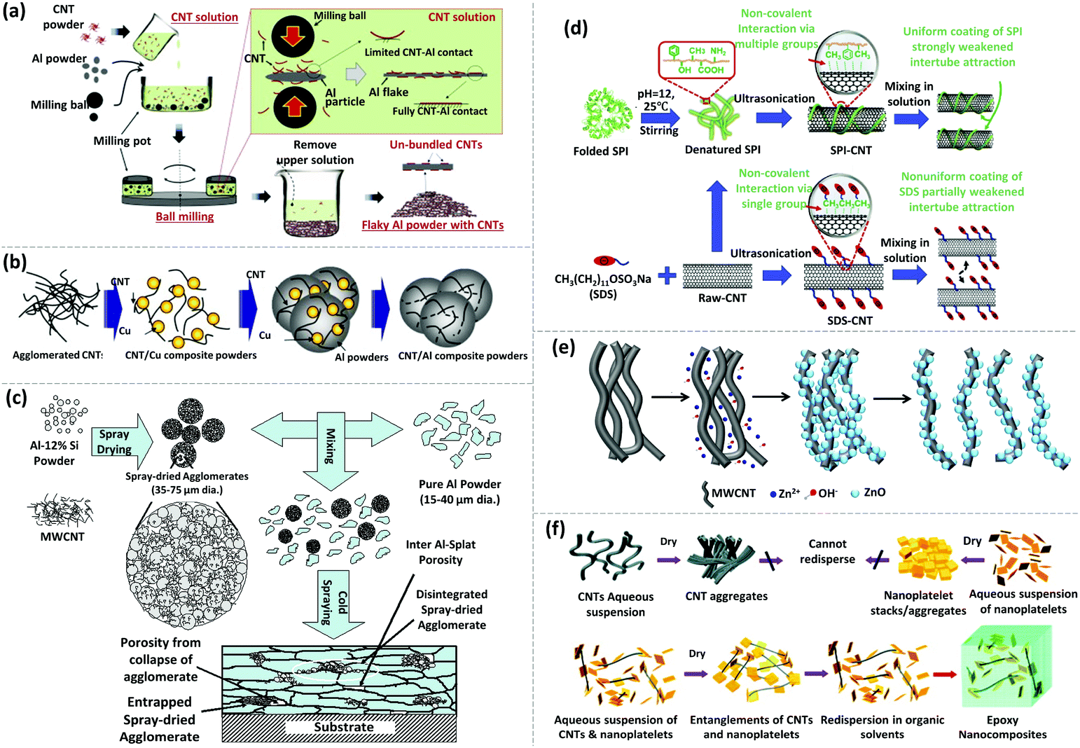 | ||
| Fig. 5 Different examples of dispersing CNTs via physical approaches and chemical modifications. (a) Schematic depiction of the solution ball milling process to disperse CNTs and Al powder into solution. Reprinted with permission from ref. 104. Copyright 2015, Springer. (b) Schematic illustration of the fabrication process of the CNT/Al–Cu composite powder. Reprinted with permission from ref. 106. Copyright 2012, Elsevier. (c) Schematic illustration of the fabrication process of the CNT–Al composite coating via cold spraying. Reprinted with permission from ref. 107. Copyright 2007, American Scientific Publishers (d). Functionalization mechanism of dispersing CNTs treated with SPI and SDS. Reprinted with permission from ref. 135. Copyright 2020, Elsevier. (e) Schematic diagram of ZnO/P-MWCNT synthesis and the formation of homogeneously exfoliated ZnO/P-MWCNTs in methanol. Reprinted with permission from ref. 138. Copyright 2017, Elsevier. (f) Schematic diagram of de-bundling and individually dispersing SWCNTs with α-zirconium phosphate (ZrP) nanoplatelet tethers. Reprinted with permission from ref. 108. Copyright 2009, Wiley. | ||
In addition, cold spraying is another possible option to prepare CNT reinforced metal composites. Agarwal et al. utilized cold spraying to prepare Al–Si eutectic powder containing uniformly dispersed MWCNTs (Fig. 5c).107 Even though the dispersion was well retained after spraying onto the substrate and embedding in the Al matrix, the lengths of MWCNTs were reduced due to the impact and shearing occurring between the Al–Si eutectic particles and the Al matrix, which could be detrimental to the overall performance of the composite coating. Generally, mechanical methods are common for the fabrication of metal–CNT bulk composites. High energy or long duration techniques can damage the structure and properties of CNTs. As a result, a combination of mild mechanical and chemical treatments is often utilized for CNT dispersion.
CNT chemical functionalization is mainly classified into covalent and non-covalent modifications. Covalent modification alters the surface chemistry of CNTs and enhances their solubility by attaching various steric and electrostatic functional groups or solvent–soluble shells to the nanotubes.108 Moreover, for metal–CNT composites, it may also create a relatively strong bonding between CNTs and the metal matrix and enhance the load transfer and the wettability. These functional groups are attached to the side walls or end caps of CNTs. The latter are often functionalized more readily due to their higher reactivity. As a result of covalent treatment, a fraction of the sp2 is converted into sp3 carbons by forming σ-bonds. Consequently, the macroscopic processability of CNTs improves while the disruption of CNT configuration usually leads to conductance reduction.76,109 Moreover, the covalent modification exfoliates the CNTs through either electrostatic repulsion or steric effects.110 On the other hand, in non-covalent modifications, surfactants, polymers, aromatic compounds, and biomolecules are adsorbed to or wrap around the CNTs.111–114 As a result, the unique structure of CNTs is persevered at a cost of introducing new impurities into the system. The exfoliation is achieved via electrostatic forces or steric hindrance effects.
Acid treatment is the most frequently employed covalent chemical modification method to increase the chemical activity and hydrophilicity of CNTs and graphene. In this approach oxygen-containing functional groups, such as hydroxyl and carboxyl groups, are covalently attached to the nanotube surface.115,116 A sonochemical oxidation method (sonication-assisted) of CNTs carried out in a sulfuric/nitric acid mixture results in the formation of carbonyl groups and carboxyl groups, with the latter being more abundant.117 Incorporation of oxygen atoms into the C structure in small amounts enhances the total density of states at the Fermi level, which is responsible for the electron injection and provides the conception of new conduction channels within the composites. The introduced functional groups can also act as inter-tube electron channels to facilitate electron conduction. However, excessive surface treatment may lead to structural damage and hinder the electron hopping phenomenon.
Coupling the acid treatment with sonication can create the desired surface defects in a shorter duration. Sonication of CNTs in nitric acid (3.0 M for 2 h) followed by hydrogen peroxide treatment (2 h) is one of the most effective routes for oxidizing CNTs without damaging their structure.118 Moreover, carboxylated CNTs produced from acid treatment can be used as precursors for further covalent modification of CNTs via esterification, thiolation, and amidation reactions. It is worth noting that the oxidative treatments disrupt the π-conjugation and create surface dipole moments, which increases the work functions of CNTs from 4.3 eV to 5.1 eV.119 As an alternative to acidized-CNTs, amino-functionalization of CNTs (ammonium bicarbonate) associated with ball milling is capable of obtaining a uniform distribution in an Al matrix. Moreover, Al4C3 is formed at the interface which acts as a transition layer. This allows for efficient load transfer from the Al matrix to amino-functionalized CNTs and improves the mechanical properties.120
Functionalization of CNTs by doping heterogeneous atoms including B, S, N, and F has received enormous interest since it can readily manipulate the properties of nanotubes.121–123 The dopant atom reacts with the CNT structure through endohedral doping (encapsulated inside the CNT's hollow core), intercalation (insertion between the C atoms), and substitution (replacing a C atom). In particular, substitutional nitrogen doping is especially of great interest since it can not only improve the electrical and mechanical properties of CNTs, but also act as an anchor to interact with neighboring metal atoms. A nitrogen atom contains one additional valence electron when compared to a carbon atom.124 This electron increases the available carrier density which leads to superior electronic performance of the doped CNTs.125 The controlled growth and selective N-doping of CNTs can be carried out via a modified floating catalyst approach with NH3, pyridine, ethylene, or xylene as a carbon source.126,127
Substitutional doping with N heteroatoms can effectively improve the adhesion of CNTs to Cu.76 The mechanical and electrical properties, and chemical reactivity of CNTs will significantly benefit from N-doping. The presence of N dopants improves the CNT bonding with metals, enhances local electron transmission through the CNTs by approximately two-fold and reduces back scattering at the Cu–CNT interface compared to the unmodified counterpart.76 Taking advantage of the abundant pyridinic groups due to high N-doping, rich defects, and various reactive sites of the bamboo-like structures, N-doped CNT composite fibers with a core–sheath structure exhibit higher specific surface area, thereby increasing their possibility of reaction with the electrolyte and enhancing the transfer efficiency.128 N-Doped CNT fibers as cathodes for Li–CO2 batteries fabricated via the floating catalyst chemical vapor deposition (FCCVD) approach demonstrated superior electrochemical performance with a full discharge capacity of 23![[thin space (1/6-em)]](https://www.rsc.org/images/entities/char_2009.gif) 000 mA h g−1, a low potential gap of 1.96 V, and up to 360 cycles of service life with decent flexibility.129
000 mA h g−1, a low potential gap of 1.96 V, and up to 360 cycles of service life with decent flexibility.129
Compared to covalent modification, the major advantage of non-covalent functionalization of CNTs is that their structure remains intact.130 Non-covalent modification employs surfactants to wrap or coat CNTs via hydrophobic interaction, π–π stacking and van der Waals interaction, which can increase CNT dispersion in a medium of interest. However, the main drawback of non-covalent modification is that the interaction between the surfactant and CNTs may not be strong enough to prevent the possibility of detachment of the surfactant during processing, which eventually leads to re-aggregation of CNTs. Moreover, surfactants often are not conductive and do not have strong interaction with metals which limits their application in metal-based systems.
SDS is perhaps the most commonly used surfactant for CNT dispersion. It is an amphiphilic anionic surfactant and the ionic negatively charged dodecyl sulfate at one end tends to attach to the surface of CNTs due to its hydrophobic affinity, while the hydrophilic groups extend outwards.131 Therefore, it can hinder CNT agglomeration by electrostatic repulsion. SDS has also been applied to assist the suspending and exfoliation of pristine CNTs to optimize the electrodeposition of Ni–CNT coatings with enhanced anti-corrosion, mechanical, and magnetic properties.132,133 In addition to effective load transfer, nickel's grain refinement caused by CNTs improves the mechanical properties. Moreover, corrosion resistance can also benefit from grain size reduction as it promotes uniform formation of a protective oxide layer.133
Soy protein isolate (SPI) is a biomolecule that can outperform SDS in terms of dispersion efficiency. It contains abundant functional groups, such as amino acids, hydrophobic aromatic, and methyl groups, to firmly wrap the CNTs and avoid agglomeration (Fig. 5d).134–136 The proteins coat the CNTs through hydrophobic or π–π interactions of their aromatic and methyl groups. On the other hand, the polypeptide chains with hydroxyl and amine ends are able to bond with the matrix. Despite SPI's highly efficient exfoliation capabilities and its amine end groups which can form strong bonds with metals, it has not yet been applied to metal composites. Besides using SDS and SPI, melamine can also be used to non-covalently functionalize CNTs in high concentrations by its interaction with CNTs’ wall via π–π stacking and providing amine end groups that can interact with metals.99 Biomolecules or surfactants with thiol ends are also able to form strong bonds with metals.
Combining covalent modifications with non-covalent ones often provides better results due to their synergistic effect. Decoration of CNTs with metallic and inorganic quantum dots (QDs) is promising to disentangle MWCNTs in organic solvents (Fig. 5e).137,138 For example, positively charged ZnO QDs decorate mildly oxidized MWCNTs in methanol due to their electrostatic attractive forces. As a result, the zeta-potential of the decorated CNTs reaches 40 mV which overcomes the van der Waals forces between the nanotubes and forms a stable homogeneous dispersion. Furthermore, the ZnO QDs increase the density of charge carriers via suppressing the scattering of electrons and promote ballistic transport of electrons between neighboring tubes by enhancing their mean free path, hence boosting the conductivity.
Based on the same mechanism, Sun et al. developed a straightforward colloidal approach to de-bundle and disperse SWCNTs via oxidation followed by the treatment of highly positively charged and exfoliated α-zirconium phosphate (ZrP) nanoplatelets (Fig. 5f).108,139 Metal nanoparticle decoration can similarly induce electrostatic repulsion forces and improve the CNT dispersion. For example, Fe nanoparticles enable magnetic functionalization of MWCNTs by simple encapsulation. These magnetic-functionalized CNTs can be employed as nano-sized adsorbents for removal of heavy metal ions from aqueous solutions.140 Au nanoparticles also have been developed to decorate SWCNTs with the manipulation of reaction temperature and the concentration of the suspension.141 A sparse decoration of Au nanoparticles on CNTs through chemical sidewall functionalization via organic linker molecules is found to achieve a low degree of CNT agglomeration on silicon wafer for a scalable on-chip functionalization. This approach seems to be promising for metal-based systems since it introduces neither structural damage nor organic impurities to the system.
3 Applications
3.1 Advanced wires
Lightweight wires are extremely attractive for aerospace and aircraft industries where just a few kilogram weight reduction can translate into thousands of dollars saving in yearly operating cost.142,143 For example, a Boeing 747 has around 250 km of wires, and most of them are made of copper with a density of 8.96 g cm−3. Automotive, portable electronics, and subsea power transmission industries among others also can significantly benefit from a lightweight conductor which can replace copper. Over the last decade a growing number of research studies have exploited the low density and remarkable electrical properties of CNTs to fabricate a new generation of conductors. CNT fibers with impressive mechanical and electrical properties and a density of only 1.6 g cm−3 have been fabricated via the wet-spinning technique. They show an electrical conductivity of up to 7.7 × 10⁶ S m−1, and mechanical strength of around 2.2 GPa.9,144–146 Moreover, these fibers have superior heat resistance and current carrying capacity which are critical factors for various applications, from satellites to miniaturized electronics. Although their electrical conductivity is very impressive, it is more than 7 times lower than that of copper. Considering its much lower density, CNT fibers still fall behind copper in terms of specific electrical conductivity (electrical conductivity divided by density).A different approach is to employ CNTs as nanofillers in metal matrices, specifically copper. Theoretical and experimental studies have shown the feasibility of achieving high electrical conductivities with low densities through compositing copper with CNTs.10,147,148 Developing a scalable method to fabricate composite wires in which CNTs and metal are intermixed is very challenging, and hence, the research has been inclined towards core–shell structures. In this approach, wet-spun CNT fibers (core) are coated with a metal (shell), typically copper. Deposition of copper is often carried out through physical vapor deposition (PVD)95,149,150 and electrodeposition,151–156 with the latter being more common since it is more cost-effective and easier to scale-up (Fig. 6a). Initial studies reported an electrical conductivity of around 2 × 10⁷ S m−1 with a density half that of copper, while the mechanical strength, current carrying capacity, and electrical conductivity at elevated temperatures often far exceeded those of copper. Recently, significant progress in terms of electrical conductivity has been achieved mainly through improving the interfacial interactions between copper and CNTs.
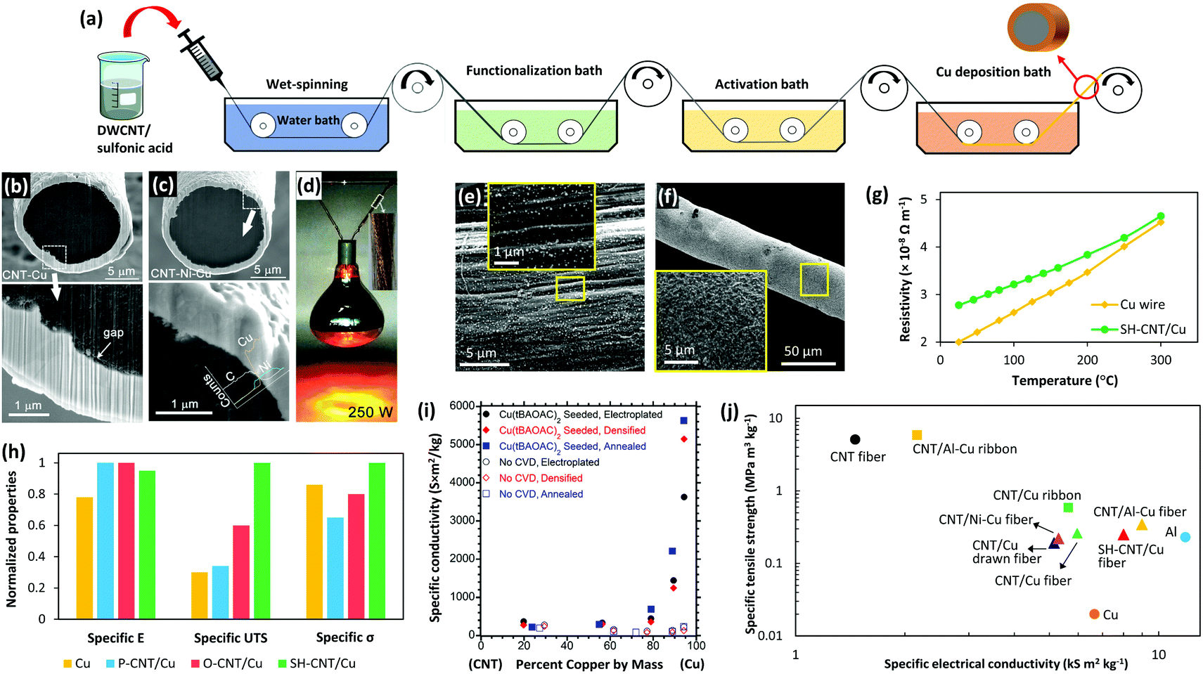 | ||
| Fig. 6 (a) Schematic of a proposed process for large-scale fabrication of CNT/Cu core–shell fibers. SEM images show the interface of CNT/Cu (b) and CNT/Ni–Cu fibers (c). (d) 100 ply CNT/Ni–Cu fibers holding and lighting a 250 W lamp. Reprinted with permission from ref. 155. Copyright 2018, American Chemical Society. (e) Uniform pre-seeding of cysteamine functionalized CNT (SH-CNT) fibers with Pd nanoparticles and (f) smooth and dense Cu coating on SH-CNT fibers. (g) Comparison of the resistivity of SH-CNT/Cu fibers with that of a commercial Cu wire at elevated temperatures showing that the core–shell fiber has more stability in terms of conductivity. (h) The effect of different surface groups (P-CNT: pristine CNTs and O-CNT: carboxylated CNTs) on the specific elastic modules (specific E), specific tensile strength (specific UTS), and specific electrical conductivity (specific σ) of the core–shell fibers and commercial Cu wire. Reprinted with permission from ref. 158. Copyright 2020, Wiley. (i) Specific conductivity of electroplated Cu–CNT hybrids with and without Cu pre-seeding. Reprinted with permission from ref. 160. Copyright 2018, American Chemical Society. (j) Ashby plot of specific strength versus specific conductivity for various CNT–metal core–shell fibers, CNT fibers, Cu, and Al. | ||
As mentioned in Section 2.3 (Interface), Cu has a full 3d orbital, and therefore, shows very poor affinity toward CNTs which causes inefficient electrical conduction. Two strategies have been implemented to improve the core–shell interfacial interactions: (i) introducing a metallic intermediate layer149,155,157 or (ii) functionalizing the outer layer of CNT fibers.156,158 Ni is an excellent choice for an intermediate layer since it has a high wettability for CNTs and also high solubility in Cu.67,68,159 Accordingly, Zou et al. electroplated a thin layer of Ni on CNT fibers prior to Cu plating and observed that both electrical conductivity and tensile strength of the core–shell fibers improved more than two fold which was attributed to the better interfacial interactions of the CNTs with the metal coating (Fig. 6b–d).155
Similarly, surface functionalization of the fibers has shown to be an effective method to improve the Cu–CNT interaction, hence enhancing the core–shell fiber properties. One of the best results has been reported recently where the introduction of cysteamine groups at the Cu–CNT interface led to an electrical conductivity of 3.6 × 10⁷ S m−1, current carrying capacity of 1.04 × 10⁵ A cm−2, and tensile strength of more than 1 GPa. The density of these fibers is only half that of copper which means that the specific conductivity, ampacity, and strength of these fibers are 12%, 100%, and 10 times higher than those of similar sized commercial copper wires.158 Cysteamine is connected to the CNTs at one end through C–C bonds and has a dangling thiol group at the other end. Thiol has a pair of free electrons which can couple with metals and form strong covalent bonding. As a result, cysteamine groups increase the wettability of Cu for CNTs and facilitate uniform deposition. Another key point is that the functionalized fibers were pre-seeded with Pd prior to Cu plating. As discussed earlier, Pd is able to effectively wet the surface of CNTs and form ohmic contacts.65 Also, these well-dispersed Pd seeds act as nucleation sites for Cu deposition which results in a uniform and dense Cu coating. Consequently, the Cu layer is strongly bonded through thiol groups and Pd seeds to the CNT fibers (Fig. 6e–h). The effect of pre-seeding is highlighted in a study by Leggiero et al. in which a chemical vapor deposition method was used to seed Cu on CNT roving before Cu plating.160 As a result, a dense and uniform CNT/Cu hybrid conductor was fabricated with an electrical conductivity of 2.81 × 10 7 S m−1, which is five times higher than that of the samples that were not pre-seeded (Fig. 6i). Another approach that is worth considering is nitrogen-doping of the CNT fibers. This has worked successfully for CNT thin films in terms of electrical conductivity and mechanical strength but has not yet been used on CNT fibers.76
On a side note, it should be added that analyses of the current carrying capacity (or ampacity) should be done with extreme care. Ampacity is not an intrinsic property of a material and it strongly depends on the environmental conditions of the test, and size and geometry of the sample. Basically, when a sample is being tested for ampacity, the current gradually increases until the resistance starts to drop. This drop is caused by the increase of sample temperature (Joule heating). Therefore, when the heat transfer around the sample is facilitated around the sample, higher values for ampacity can be obtained. The ambient temperature, air flow, and even the type of gas in which the experiment is being carried out can affect the outcome. For example, when the sample is a thin film or has very small dimensions, it has a more effective heat transfer with the surrounding environment.147,161 Thus, it takes more current to increase its temperature. Consequently, one should refrain from quantitatively comparing the results of thin films or small samples with those of a bulk material.
The confluence of electrical, thermal, and mechanical property enhancements that the CNT/Cu core–shell structures offer leads to tremendous potential of these materials as electrical cable conductors (Fig. 6j). However, several challenges need to be overcome before seeing their widespread adoption, namely, manufacturing cost and scalability, length and quality of CNTs, Cu–CNT interfacial interaction, and the quality of the Cu deposits. Further improvement can be obtained by adding extrusion as the final step of the wire production process. Implementing extrusion not only improves the smoothness, but also densifies the Cu coating, which can lead to superior electrical and mechanical properties.150 This step can be done at elevated temperatures in an inert environment to avoid coating detachment/slippage.
Thus far, the strength of these fibers is far superior to that of commercial Cu wires. Therefore, the attention should be shifted towards improving the electrical conductivity. The long-term reliability of these fibers needs to be evaluated as well. More specifically, the adhesion between CNTs and the metal should be studied possibly through bending tests for a long duration. Another important issue that is often overlooked is the oxidation of the metal in contact with the CNTs. When two dissimilar metals are in contact, a galvanic cell forms which leads to the corrosion of the metal with the lower redox potential. As the difference between the redox potentials increases, the corrosion will be more serious. CNTs have a redox potential in the range of +0.38 to +0.8 V (versus SHE).162,163 Therefore, galvanic corrosion for Cu (+0.35 V) in contact with CNTs is negligible, but the CNT contacts with Ni (−0.22 V) and specifically Al (−1.7 V) need to be explored. Finally, special attention must also be paid to the behavior of the materials throughout the fabrication process. For example, CNT fibers can swell and lose their integrity if they are immersed in aqueous solution for long periods.
3.2 Field-effect transistors
Nanotechnology has been pivotal in advancing computing and electronics, leading to faster, smaller, lighter, and more energy efficient products. This has been achieved through miniaturization of microprocessors and their main component: metal–oxide–semiconductor field-effect transistor (MOSFET) (Fig. 7a).164 A simplified diagram of a MOSFET is presented in Fig. 7b. When voltage is applied to the gate terminal which is situated on top of an insulator, an electrical field is formed inside the channel, causing current to travel from the source to drain. Simply, a MOSFET is a switch for the flow of current; when voltage is applied, current goes through the channel creating the on-state, and when voltage is cut off, current stops and the transistor is in the off-state. This off/on state is analogous to 0/1 used in binary logic. Over the years, the size of these components has been shrinking to place more transistors on integrated circuits and enhance the processing power.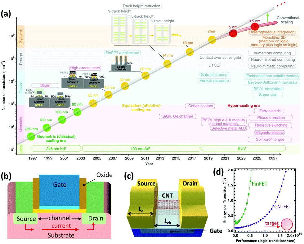 | ||
| Fig. 7 (a) The evolution of transistor density scaling. Reprinted with permission from ref. 164. Copyright 2018, Nature. (b) Simplified schematic of a MOSFET. (c) Simplified schematic of a CNTFET (LC: contact length and Lch: channel length). (d) Performance versus energy consumption of a CNTFET and a fin field-effect transistor (FinFET) which is currently a common architecture of MOSFETs. Ideally a transistor should have low energy consumption and high performance. Reprinted with permission from ref. 166. Copyright 2014, American Chemical Society. | ||
For the past 50 years, this scaling was made possible with minor design and material modifications. However, as the industry is moving towards 5 nm and smaller size technologies, there is a concern that conventional silicon-based materials are reaching their physical limits. Therefore, there is growing interest to develop new materials that can make the future scaling possible. Semiconductor CNTs (S-CNTs) with their excellent current carrying capacity, high carrier velocity, and nanoscale diameter are known to be some of the promising candidates for this purpose. In CNT-based transistors, which are also known as field-effect transistors (CNTFETs), S-CNTs are used as the channel material. In this case the source and drain which are metallic are in direct contact with the S-CNTs (Fig. 7c). Consequently, the metal–CNT interface has a critical role in the performance of the CNTFET.165
Compared to commercial MOSFETs, CNTFETs offer minimal current leakage in the off state, can work with lower voltages (better energy-efficiency), and have 2.5–10 times higher saturation velocity for carriers (Fig. 7d).166 There are several major hurdles for commercial application of CNTFETs, particularly their high contact resistance (RC) and poor interfacial interactions at the metal–CNT junction. These challenges have been widely investigated in the literature and some promising results have been reported. As discussed in Sections 2 and 3 (Interface), ohmic or low barrier Schottky contacts are desired for metal–CNT junctions. Studies have shown that parameters such as metal type, contact length, CNT diameter, and metal deposition method can influence the RC in CNTFETs.164–171 The correlation between some of these parameters and RC is straightforward. For example, the contact length is inversely proportional to RC or by increasing the S-CNT diameter, the RC decreases and the optimal value can be achieved by using S-CNTs with diameters above 1.4 nm.167,168 On the other hand, selection of the right metal is more complex and is determined by a few interrelated concepts which will be discussed further.
Metals with high work functions are able to form low RC junctions with CNTs. S-CNTs in contact with these metals turn into p-type semiconductors, and holes become the majority carriers.167 Metals such as Pd, Au, and Pt with the work function between 5 and 5.6 eV fall into this category. In contrast, S-CNTs in contact with metals with low work function lend themselves to n-type semiconductors favoring electrons as the charge carrier.169 Metals such as Er, Y, and Sc were used as contacts which showed excellent performance for large contacts, but fail to function after size reduction since they readily oxidize.81,169–172 Therefore, metals with high work function are more attractive candidates. Among them, Pd shows the best performance mainly due to its high wettability for CNTs and weak hybridization at the interface which leads to side-contacts that have no or very low Schottky barrier.75,159,161,168
As the next efforts focused on scaling CNTFETs, it was discovered that when the contact length scales down to 20 nm and beyond, Pd does not necessarily have the best performance. By testing Au, Pt, Pd, Ti, Ni, and Rh for scaled contact lengths, it was revealed that Rh has the best scaling behavior and its RC is less influenced by the contact length, making it a promising candidate for contact lengths below 20 nm (Fig. 8a).170 The reason behind this trend is not clear but scientists at IBM believe that the transport regime and charge carrier injection mechanism possibly change at sub-20 nm contact lengths. For example, as it can be observed in Fig. 8b, the RC at 70 nm Pd contacts decreases by increasing the temperature which is an indication of Schottky resistance. However, for a 20 nm contact length, the RC becomes independent of the temperature, implying that the mechanism of charge transfer from S-CNTs to Pd contact has changed.170 Additional theoretical and experimental research is required to shed light on the electrical transport mechanism in scaled channels and contact lengths.
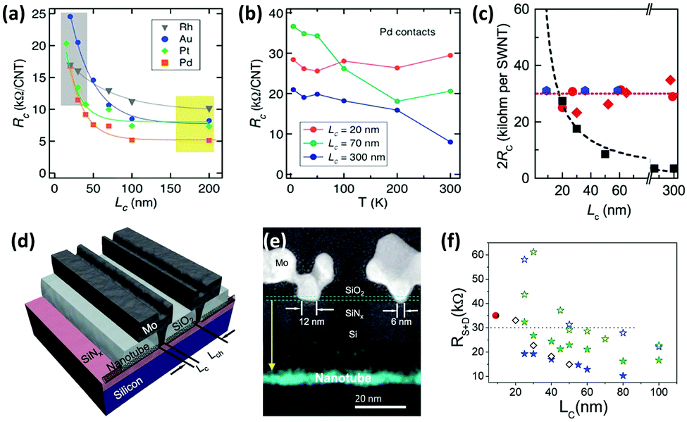 | ||
| Fig. 8 (a) RC of different metals versus the contact length. (b) The resistance of Pd side-contacts at elevated temperatures with various contact lengths (LC). Reprinted with permission from ref. 170. Copyright 2014, American Chemical Society. (c) Comparison of 2Rc as a function of LC for Mo end-contacts for different SWCNTs (blue and red) and best Pd side-contacts. (d) Schematic of a Mo end-contacted nanotube transistor and (e) dark field STEM image of its cross section. The corresponding carbon EDX map of the transistor before Mo deposition, shows the SWCNT on the substrate. Reprinted with permission from ref. 75. Copyright 2015, AAAS. (f) Scaling characteristics of contact resistances for Pd (blue stars) and Sc (olive stars) side-contacts (RS+D ≈ 2RC). Solid stars represent the device based on a 1.5 diameter SWCNT and open stars are for a 1.1 nm diameter SWCNT. Hollow diamonds are for Pd side-contacts reproduced from ref. 170 and the solid red sphere is for the Mo end contact reproduced from ref. 75. Reprinted with permission from ref. 171. Copyright 2017, AAAS. | ||
Another factor that can improve the RC at the source/drain–CNT interface is the contact geometry. Due to the simplicity of the fabrication process, in most previous studies, side-contacts have been employed. However, numerous reports have indicated that end-contacts can yield superior conductivity.72 DFT calculations on end-contacts of CNTs with Pd and Cu lead to RC values of 142 kΩ and 253 kΩ, which show almost 60- and 2500-times improvement compared with their side-contacts, respectively. Moreover, by comparing the results for end-contacts, one can conclude that the resistance values are relatively close to each other, meaning that the difference between various metals diminishes for end-contacts.
One experimentally successful approach is creating carbides at metal–CNT end-contacts. If the metal has high work function and solubility for carbon, it can form carbides at elevated temperatures. Consequently, an abrupt junction with low RC will be achieved. Mo has the requirements for such a contact and results have shown that its RC does not change with extreme scaling and is stable at around 17.5 kΩ for contact lengths of below ∼9 nm (Fig. 8c–e).75 Meanwhile, the best results for Pd side-contacts are ∼18.5 kΩ for 10 nm contact length and 10 kΩ for 20 nm contact length.85,171 Increasing the diameter of the nanotubes can also improve the Pd side-contact resistance (Fig. 8f). Nevertheless, further scaling of Pd contacts will lead to a drastic increase in resistance while Mo end-contacts are not affected by contact length.
Despite remarkable performance, the commercial adoption of Mo end-contacts may be hindered by their high fabrication temperature; Mo carbides are formed at around 850 °C. Alternatively, Mo can be alloyed with Co which yields similar low RC junctions, but as an advantage, it can form carbides at lower temperatures (650 °C). Cao et al. used a Mo (50 at%)–Co alloy as the contact material and fabricated a 40 nm CNTFET with contact and channel lengths of 10 nm and sub-10 nm.92 For comparison, the contact length of a state-of-the art 7 nm Si MOSFET is around 25 nm.85 This device showed a leakage of only 4 nA at a low driving voltage of 0.5 V, on-current Ion value up to 0.8 mA μm−1, and Ion/Ioff ratio of ∼103. These results already surpass those of Si-based FETs, showing great potential for extremely scaled CNTFETs.
Finally, it is worth noting that another major progress was achieved through modifying the design of CNTFET contacts (Fig. 9). Back-gated CNTFETs were the first employed design in which metallic contacts were deposited on a silicon dioxide substrate and subsequently S-CNTs were randomly placed on top of the contacts. Although the processing is simple, these CNTFETs require high voltages to operate and have a high Schottky barrier at the interface due to poor adhesion and small contact area. Ultimately, top-gated, suspended, and gate-all-around designs were developed with superior performance. Among them, top-gated CNTFETs are simpler and commonly used to fabricate high performance CNTFETs.75,85,92,113,171 In a gate-all-around architecture, a CNT is completely surrounded by the contact which is natural to the CNT's shape and gives superb electrostatic control over it.173 It is expected that gate-all-around would yield lower leakage current due to superior electrostatic control and higher on/off ratio, making it a promising candidate for future devices.174
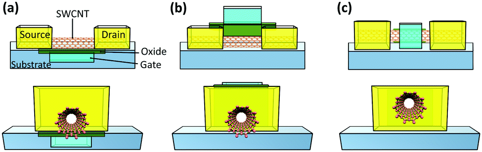 | ||
| Fig. 9 Schematic of CNTFETs with back-gate (a), top-gate (b), and gate-all-around (c) architectures. | ||
3.3 Transparent electrodes and stretchable electronics
Transparent conductive electrodes (TCEs) are at the interface of many electronic devices with widespread applications in liquid crystal displays, wearable electronics, and as touch screens in smart phones and laptops. Derived by the rapid growth of consumer electronics, the TCE market is expected to have substantial growth in the coming years, reaching USD 8.46 billion by 2026. This growth rate will likely rise by the advent of Covid-19 pandemic as businesses and educational institutions are universally transitioning to working remotely. In addition, TCEs are extensively used in photovoltaics and the boost of the solar energy industry can fuel the demand for TCEs even further.Simply, the main requirements of a TCE are low sheet resistance (RS) and high transparency. Indium tin oxide (ITO) is the most commonly used material in TCEs. It exhibits low RS typically ranging from 10 to 50 Ω □−1 at a transmittance above 85%.174,175 Despite this excellent optoelectrical performance, its high cost, redox activity, and brittleness have motivated researchers to develop new alternatives.176 One option is metal-based electrodes which generally have higher ductility and electrical conductivity. Metal-based TCEs are mainly fabricated by using nanowires (NW) or spun fibers made of Ag. Ag nanowire-based TCEs can have a low sheet resistance (10 < Rs < 50 Ω □−1) at a high transmittance (T > 80%).175,177–179 However, Ag is even more expensive than indium which defeats the purpose of finding a cheaper alternative. Nanowires made of Cu which costs 1% of silver are a more cost-effective option.180 Their conductivity–transmission performance is similar to that of their Ag-based counterparts, but they are susceptible to oxidation.181–184 In addition to oxidation, inherent high light reflection (hazy appearance) coupled with temperature-dependent performance limits the scope of metal-based TCEs' applications. Therefore, the search for a suitable option to replace ITO continues.181,185
CNTs are among the various materials that have been investigated for TCEs and stretchable electronics. They possess the main requirements needed: high electrical conductivity and transmittance for neutral color. Moreover, they are flexible, possess high chemical and performance stability, and can be easily processed at room temperature. For fabrication, CNTs are usually dispersed in a solvent and then deposited on a transparent flexible polymer via spin coating, dip coating, spray coating, electrophoretic deposition, or vacuum filtration. For TCE applications, there are several parameters that affect the performance, but generally long metallic SWCNTs with good dispersion that are randomly distributed are desired. Although remarkable results have been achieved (RS of 25 Ω □−1 at a visible light transmittance of around 90%) generally CNT-based TCEs have inferior performance compared with ITO, mainly due to their dispersion issues and high contact resistance.186
It has been shown that doping the CNT network through metallic nanoparticle hybridization or chemical treatment can improve the optoelectronic performance.186–190 This is attributed to the shifting of CNTs' Fermi level upon doping which leads to charge carrier injection (Fig. 10).176 As a result, not only the conductance of individual CNTs increases but also the Schottky barrier at the interface of metallic and semiconducting CNTs reduces. This is critical since in a conductive network, the resistance is dominated by the inter-fiber resistance. Chemical treatment which pertains to reacting CNTs with acids (H2SO4, HNO3, HCl) or chemicals such as SOCl2 and AuCl3 is a facile process but it has temporary effects since the dopants are not stable and readily desorb from the network.191 Hybridization with metals provides an effective and more stable approach for improving the optoelectronic performance of CNT networks.176
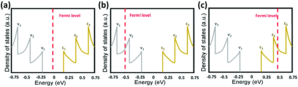 | ||
| Fig. 10 Density of states as a function of energy of S-SWCNTs: (a) no doping, (b) p-doping, and (c) n-doping. v1, v2, v3, c1, c2, and c3 indicate different levels of the valence and conduction band. Reprinted with permission from ref. 176. Copyright 2016, American Chemical Society. | ||
Metal hybridization of CNTs is carried out either by CNT surface decoration with metal nanoparticles or by compositing with metal nanowires (NW). Metals such as Pd, Pt, Ag, Au, and Cu have been used for this purpose.163,176,187,188 Metal nanoparticles are often deposited on CNTs through grafted organic functional groups. When metals with high work function such as Au or Pd are used, the electrons migrate to the metal, which increases the density of the holes in the CNTs, hence the conductivity of the network enhances. Moreover, the work function of the CNT network can be tuned depending on the metal type.188 This can be of a great advantage when the CNT network is connected to a metallic contact and the Schottky resistance can be reduced by adjusting the CNTs’ work function.189 Metal–CNT hybridized structures often show a superior optoelectrical performance compared with bare CNT networks.163,187,192,193 For instance, Lee et al. grafted Ag nanoparticles terminated with amine groups to carboxyl groups on DWCNTs and observed that after annealing, the Rs of the TCE decreased from around 1000 Ω □−1 to 45.8 Ω □−1 at 90.4% transmittance.193 Similarly, Yang et al. reported an 81% decrease in sheet resistance after doping SWCNTs with Au nanoparticles, achieving a sheet resistance of 90 Ω □−1 at 83% transmittance.192
Although metal doping has been proven to improve the optoelectronic performance of CNT networks, in recent years it has been replaced by conductive polymers since they yield the same deliverables but at a lower cost. Plus, even after doping with rare and expensive metals, CNT-based TCEs’ performance is not as good as that of metal nanowire (NW) systems.175,194,195 Another strategy is to composite CNTs with metal NWs and it has provided remarkable results.196–199 For example, Zhong et al. fabricated a highly uniform mesh of Ag-MWCNTs that showed an excellent RS of 8.92 ± 0.26 Ω □−1 and 95.05% transmittance at a wavelength of 550 nm.198 The TCE was made by spin-coating the CNT–Ag nanoparticle ink on a PET substrate followed by lithography to create the patterned mesh (Fig. 11). Due to the CNTs’ mechanical strength and strong adhesion to the PTE, this TCE showed remarkable flexibility, retaining its excellent optoelectronic performance after severe bending and washing cycles. Moreover, MWCNTs effectively act as a conducting bridge for Ag nanoparticles when they are under mechanical stress, which can be explained by the high wettability of Ag for CNTs.
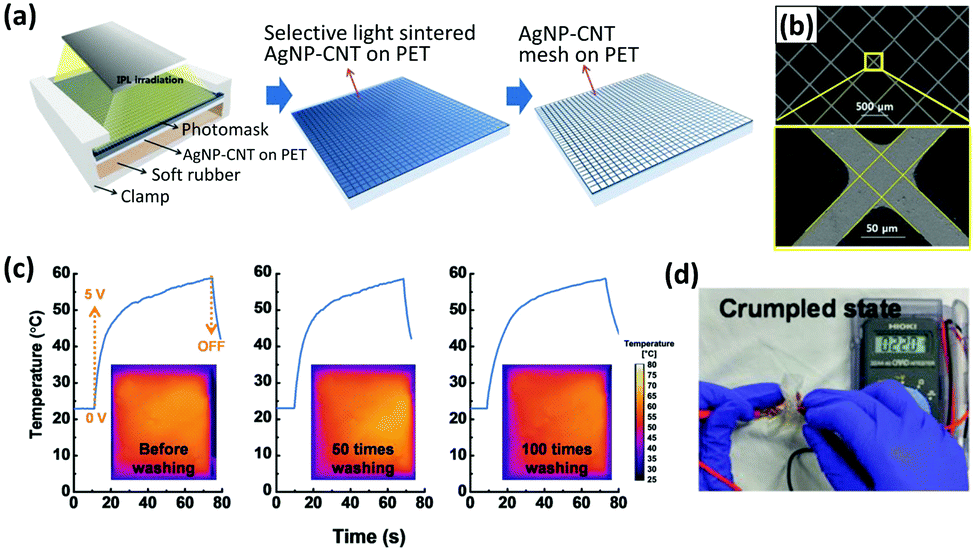 | ||
| Fig. 11 (a) Schematic diagram of the selective light-induced patterning technique for fabricating a fine and uniform AgNP–CNT mesh. (b) The microscopic image of the AgNP–CNT mesh. (c) Temperature evolution of the TCH at an applied voltage of 5 V as a function of washing times ranging from 0 to 100 times. (d) The transparent mesh retains its conductivity after 100 cycles of washing and rinsing, showing its high flexibility. Reprinted with permission from ref. 198. Copyright 2018, Wiley. | ||
In a recent study, CNT–Cu composite fibers were fabricated via electrospinning and they showed excellent performance stability at high temperatures and high currents.199 To produce the randomly distributed CNT–Cu TCE, a mixture of functionalized CNTs, Cu NWs, CuNO3, and PVA was used as the electrospinning precursor (Fig. 12a). The interfacial interaction between Cu and CNTs was enhanced through grafting cysteamine to the surface of CNTs, which played a critical role in the processing and properties of the TCE. Electrospinning may create fine nanoparticles instead of a continuous fiber in inorganic systems. However, Cu NWs alongside the functionalized CNTs act as bridges to form long continuous fibers leading to significantly improved electrical properties. Owing to CNTs' high current carrying capacity and thermally assisted charge transfer,200,201 this composite network shows a stable performance in a wide range of bias fluctuations and temperatures (Fig. 12b–e), contrary to common metal-based TCEs. A sheet resistance of 39 Ω □−1 at 81% transmittance is achieved.199 Superior performance is expected if a patterned mesh is fabricated with this precursor, for example, through melt spinning, ink-jet printing, or adopting a similar approach used by Zhong et al.198
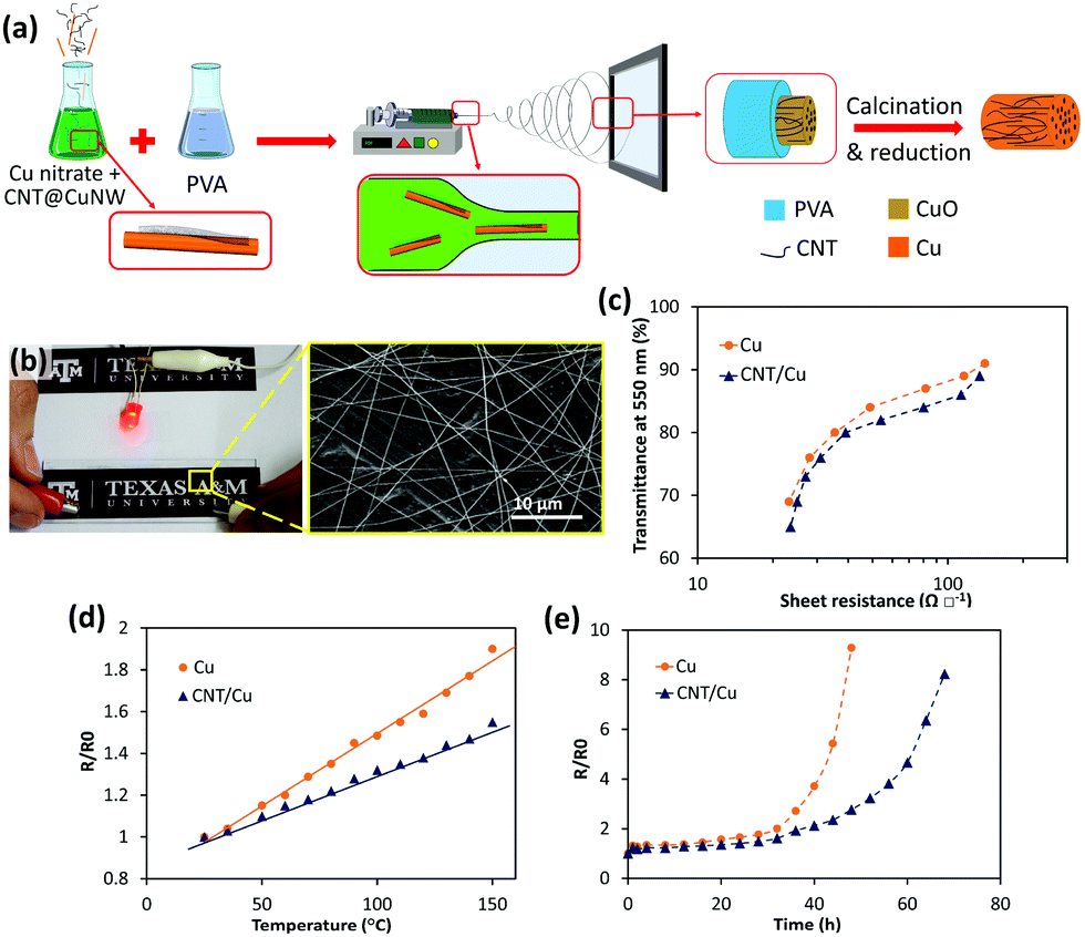 | ||
| Fig. 12 (a) Schematic of the electrospinning process for fabrication of CNT/Cu fibers. (b) TCE of random CNT/Cu fibers lighting an LED lamp. (c) Transmittance at 550 nm versus sheet resistance of TCEs made of Cu and CNT/Cu fibers. Comparison of the performance of CNT/Cu and Cu TCEs at (d) high temperatures and (e) under a high constant current of 40 mA. Reprinted with permission from ref. 199. Copyright 2020, American Chemical Society. | ||
3.4 Energy storage
Rechargeable batteries and supercapacitors are essential components of today's portable electronics. High surface area, aspect ratio, and chemical stability coupled with excellent conductivity and mechanical properties make CNTs an ideal candidate as a building block for energy storage systems. Initially, CNTs were recommended to replace carbon black in Li-ion battery electrodes. Their high aspect ratio leads to a much smaller percolation threshold compared with carbon black, which means a conductive network can be obtained in a much smaller loading.166 They have also been utilized as substrates for active materials in metal oxide supercapacitors.202,203 In these systems, CNTs provide a robust and conductive backbone which facilitates charge transfer, minimizes aggregation of metal oxides, and increases the surface area. CNTs have also been implemented in the anode of rechargeable batteries as a substitute for conventional graphite and as a current collector. In recent years, it has been shown that engineering the surface chemistry can significantly enhance CNTs' performance in batteries and supercapacitors. Thus far, most of the discussions pertained to CNTs' interfacial interactions with transition metals, but in this section, the focus will be on alkali metals with applications in electrochemical energy storage systems, namely Li, Na, and K.As mentioned before, CNTs' surface has poor interfacial interactions and is not easily wetted by metals or polar liquids like water. This can have a detrimental effect on their efficiency in energy storage systems where Li, Na, and K are prevalently used either as the active material or in electrolytes. In the anodes of Li and Na-ion batteries (LIBs and SIBs, respectively), poor wettability can lead to non-uniform nucleation and dendritic growth during continuous Li or Na plating/stripping cycles. These dendrites can penetrate through the separator and cause short-circuiting which can lead to rapid overheating or even ignition.204 CNT functionalization with oxygen surface groups via acid treatment or oxygen microwave plasma has been shown to be a successful method to reduce the localized overpotential, increase binding sites, and promote lateral growth (Fig. 13a and b).205,206 Moreover, by decreasing the surface energy, carboxyl groups increase the electrolyte wettability for CNTs which facilitates the metallic ion diffusion into the electrode structure and increases the binding energy. Implementation of this method has shown promising results for Na–air batteries, where oxygen functionalization produces a “sodiophilic” anode with an ultrahigh capacity of 1078 mA h g−1, close to pure sodium’s theoretical capacity (1166 mA h g−1), and a long cycle life up to 3000 cycles. Functionalization with cysteamine is another covalent method that has shown positive effects on the performance of CNT-based supercapacitors, but the reports on this matter are scarce.204,205,207
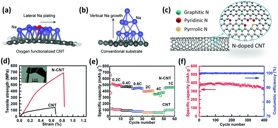 | ||
| Fig. 13 Schematic of Na growth behavior on (a) functionalized CNTs and (b) conventional Cu foil surfaces by DFT calculations. Reprinted with permission from ref. 205. Copyright 2019, Wiley. (c) N atom configuration in N-doped CNTs. Adopted with permission from ref. 28. Copyright 2020, Elsevier. (d) Stress–strain curves of CNT sheets and N-CNT films. The inset presents a photograph of a bendable N-CNT film. Comparison of the electrochemical performance of N-CNT and CNT films as anodes in Li-ion batteries: (e) specific capacity over cycling at different rates, and (f) capacity retention and coulombic efficiency. Reprinted with permission from ref. 212. Copyright 2016, Wiley. | ||
Despite these remarkable results, there is always a major concern associated with oxygenation or carboxylation treatments: they have destructive effects on the microstructure and electrical conductivity of graphitic nanostructures.76,208 Substitutional doping with elements such as N, F, and S can also improve the performance of the energy storage systems. Among various dopants, N-doping is more prominent since it not only enhances the CNT wettability and interfacial interactions with alkali metals but also improves its electrical conductivity.208,209 The most common method for N-doping is synthesizing CNTs at high temperature in the presence of NH3. The N-defects in graphitic nanostructures often have three configurations: pyridinic nitrogen, pyrrolic nitrogen, and graphitic nitrogen (Fig. 13c). N-Doping plays a pivotal role in enhancing energy storage in LIBs and supercapacitors (Fig. 13d–f). Several mechanisms have been proposed for energy storage enhancements in these systems. Concisely, N-doping can (i) open gates for metal ions to have access to the interwall, providing more surface area for energy storage, specifically in the pyridinic configuration;210,211 (ii) improve the wettability and therefore facilitate metal diffusion by creating permanent dipoles around C–N bonds due to its higher electronegativity than C;76,212 (iii) increase the electrical conductivity of CNTs through increasing the density of states at the carbon's Fermi level;69,213 and (iv) provide more bonding sites for Li, Na, and K because N-defects can donate electrons to metallic ions.69
In addition, by N-doping in supercapacitors the energy storage mechanism changes from surface-controlled pure capacitive (non-faradaic) to diffusion-controlled pseudo-capacitive.211,214 Similarly, in the anodes of SIBs and Na–air batteries N-doping of graphitic structures improves the wettability, suppresses dendritic growth, and enhances the electrical conductivity of the electrode which results in higher energy storage capacity.204,209,215 For instance, Zhao et al. fabricated a 3D scaffold as an anode of SIBs using N-doped CNTs and carbon paper.209 They observed that N-doped CNTs can effectively improve the wettability between the anode and liquid metal Na, creating a sodiophilic anode. As a result, the current was distributed evenly on the surface of the anode which led to lateral and uniform growth of the Na layer during charge/discharge cycles. It is worthy of note that S-doping has also been implemented to modify the CNT–Na interactions in SIBs with promising results.215,216 Similar to N-defects, S-doping also promotes the catalytic activity for uniform nucleation and growth of Na, improving the high rate performances of batteries.209,216
Non-covalent methods such as metal oxide coating, conjugation with conductive polymers, and metal decoration are other successful approaches for improving the interfacial interactions and wettability of CNTs for Li, Na, and electrolytes in electrochemical storage systems.202,217,218 One of the best results for Cu oxide-based supercapacitors in the literature was only achieved after introducing an intermediate SnO2 layer between Cu and CNTs. SnO2 has excellent wettability for CNTs and high interaction with CuxO, acting as a conductive “glue” between the active material (CuxO) and the substrate (CNTs). This not only facilitates the electron transfer between them but also provides abundant nucleation sites for the active material, leading to a fine structure with enhanced surface area.202
The energy storage capacity benefits from incorporation of CNTs due to their high electron mobility, mechanical strength, surface area, thermal conductivity, and their unique structure. However, the relatively high cost remains a major hurdle for widespread commercial application of CNTs. All these results indicate the significance of interface engineering and surface functionalization of CNTs and similar carbon nanostructures for enhancing the energy storage capacity in future electronics.
4 Conclusions and outlook
Excellent electronic and mechanical properties coupled with low density make CNTs an attractive option for future electronics. In many potential applications, CNTs need to be incorporated alongside metals. Interaction of these two different materials presents some unprecedented challenges. In this review, these corresponding challenges, latest breakthroughs, and a number of potential applications that can exploit CNT–metal systems were discussed.Poor interfacial interaction has been a major hurdle to realize the full potential of CNT–metal systems. In light of the numerous theoretical and experimental studies, today we have a better understanding of the chemistry behind CNT–metal interactions. Variables such as metal type and the contact geometry dictate the nature of their binding. Novel processing techniques including ALD, pre-seeding, or forming carbides through laser ablation can improve the wettability and interfacial interactions. Although the contact resistance close to the quantum limit of CNTs (6.5 kΩ) has already been achieved,75,171 our understanding of the electronic properties at CNT–metal junctions is limited specifically in scaled dimensions and in the presence of defects. At scaled junctions, the charge carrier transfer has possibly a different mechanism that cannot be explained by known theories.170 Therefore, new systematic studies are required to test different metals at <10 nm contacts because metals that yield low ohmic contacts at a larger scale may not have the best performance at smaller scales. Moreover, defects and functionalization groups have shown to enhance the electrical, mechanical, and even electrochemical properties of the CNT–metal composites. N-Doping for example holds great promise as it not only increases the CNT wettability by metals but also can improve the electronic properties of the CNTs. Through engineering the interface, lightweight thin-films and wires have been fabricated which exceed common metals in terms of specific conductivity, strength, and current carrying capacity, showing their great potential on the macroscale. Further research on functionalized CNT-based systems on the nanoscale is highly desired which can lead to low resistance ohmic and robust CNT–metal contacts, benefiting a wide range of industries from processors to TCEs.
There has been remarkable progress in terms of fabrication and precise sorting of CNTs, paving the way towards highly conductive CNT fibers or CNTFETs that surpass the commercial Si-based MOSFETs in many key aspects. But there is still a long road ahead for large-scale application of CNTs. High price of CNTs is a major obstacle for commercial applications, leaving these structures only for some high-end products. There are still other issues that need scientists' attention before their wide-spread application. Safety and toxicity analysis of CNTs in occupational environments is crucial as there are concerns over long-term exposure to them through skin contact and inhalation. Another aspect that has been neglected is the long-term performance of the CNTs adjacent to the metals as they can form a galvanic cell with the metal, leading to metal oxidation and corrosion.
Conflicts of interest
There are no conflicts to declare.Acknowledgements
The authors acknowledge the financial support of the Lloyd's Register Foundation, London, UK, which has funded this research through their grants to protect life and property by supporting engineering-related education, public engagement, and the application of research (grant G0083).References
- L. Langer, V. Bayot, E. Grivei, J.-P. Issi, J. Heremans, C. Olk, L. Stockman, C. Van Haesendonck and Y. Bruynseraede, Phys. Rev. Lett., 1996, 76, 479 CrossRef CAS.
- X. Zhou, J.-Y. Park, S. Huang, J. Liu and P. L. McEuen, Phys. Rev. Lett., 2005, 95, 146805 CrossRef.
- T. Ebbesen, H. Lezec, H. Hiura, J. Bennett, H. Ghaemi and T. Thio, Nature, 1996, 382, 54–56 CrossRef CAS.
- M. Radosavljević, J. Lefebvre and A. Johnson, Phys. Rev. B: Condens. Matter Mater. Phys., 2001, 64, 241307 CrossRef.
- E. T. Thostenson, Z. Ren and T.-W. Chou, Compos. Sci. Technol., 2001, 61, 1899–1912 CrossRef CAS.
- Z. Han and A. Fina, Prog. Polym. Sci., 2011, 36, 914–944 CrossRef CAS.
- C. Subramaniam, Y. Yasuda, S. Takeya, S. Ata, A. Nishizawa, D. Futaba, T. Yamada and K. Hata, Nanoscale, 2014, 6, 2669–2674 RSC.
- B. Kumanek and D. Janas, J. Mater. Sci., 2019, 54, 7397–7427 CrossRef CAS.
- D. E. Tsentalovich, R. J. Headrick, F. Mirri, J. Hao, N. Behabtu, C. C. Young and M. Pasquali, ACS Appl. Mater. Interfaces, 2017, 9, 36189–36198 CrossRef CAS.
- O. Hjortstam, P. Isberg, S. Söderholm and H. Dai, Appl. Phys. A: Solids Surf., 2004, 78, 1175–1179 CrossRef CAS.
- M. Zhao, Y. Chen, K. Wang, Z. Zhang, J. K. Streit, J. A. Fagan, J. Tang, M. Zheng, C. Yang and Z. Zhu, Science, 2020, 368, 878–881 CrossRef CAS.
- A. D. Franklin, Science, 2015, 349, 6249 CrossRef.
- L.-M. Peng, Z. Zhang and C. Qiu, Nat. Electron., 2019, 2, 499–505 CrossRef CAS.
- M. Pumera and Y. Miyahara, Nanoscale, 2009, 1, 260–265 RSC.
- C. Ge, Y. Li, J.-J. Yin, Y. Liu, L. Wang, Y. Zhao and C. Chen, NPG Asia Mater., 2012, 4, e32 CrossRef.
- J. Vejpravova, B. Pacakova and M. Kalbac, Analyst, 2016, 141, 2639–2656 RSC.
- Z. Yang, J. Tian, Z. Yin, C. Cui, W. Qian and F. Wei, Carbon, 2019, 141, 467–480 CrossRef CAS.
- N. Matsumoto, G. Chen, M. Yumura, D. N. Futaba and K. Hata, Nanoscale, 2015, 7, 5126–5133 RSC.
- M. Pumera, A. Ambrosi and E. L. K. Chng, Chem. Sci., 2012, 3, 3347–3355 RSC.
- M. Pumera, Chem. Rec., 2012, 12, 201–213 CrossRef CAS.
- A. Ambrosi and M. Pumera, Chem.–Eur. J., 2010, 16, 10946–10949 CrossRef CAS.
- U. J. Kim, C. A. Furtado, X. Liu, G. Chen and P. C. Eklund, J. Am. Chem. Soc., 2005, 127, 15437–15445 CrossRef CAS.
- Y. Wang, H. Shan, R. H. Hauge, M. Pasquali and R. E. Smalley, J. Phys. Chem. B, 2007, 111, 1249–1252 CrossRef CAS.
- P.-X. Hou, C. Liu and H.-M. Cheng, Carbon, 2008, 46, 2003–2025 CrossRef CAS.
- D. J. Babu, S. Yadav, T. Heinlein, G. Cherkashinin and J. r. J. Schneider, J. Phys. Chem. C, 2014, 118, 12028–12034 CrossRef CAS.
- N. Berrada, A. Desforges, C. Bellouard, E. Flahaut, J. Gleize, J. Ghanbaja and B. Vigolo, J. Phys. Chem. C, 2019, 123, 14725–14733 CrossRef CAS.
- G. Tobias, L. Shao, C. G. Salzmann, Y. Huh and M. L. Green, J. Phys. Chem. B, 2006, 110, 22318–22322 CrossRef CAS.
- F. Daneshvar, T. Zhang, A. Aziz, H.-J. Sue and M. E. Welland, Carbon, 2020, 157, 583–593 CrossRef CAS.
- A. Ismail, P. S. Goh, J. C. Tee, S. M. Sanip and M. Aziz, Nano, 2008, 3, 127–143 CrossRef CAS.
- R. Das, M. Ali, S. Bee Abd Hamid, M. Annuar and S. Ramakrishna, J. Nanomater., 2014, 2014, 945172 Search PubMed.
- A. L. Antaris, J. T. Robinson, O. K. Yaghi, G. Hong, S. Diao, R. Luong and H. Dai, ACS Nano, 2013, 7, 3644–3652 CrossRef CAS.
- M. Bystrzejewski, A. Huczko, H. Lange, T. Gemming, B. Büchner and M. Rümmeli, J. Colloid Interface Sci., 2010, 345, 138–142 CrossRef CAS.
- X. Deng, D. Xiong, H. Wang, D. Chen, Z. Jiao, H. Zhang and M. Wu, Carbon, 2009, 47, 1608–1610 CrossRef CAS.
- A. R. Harutyunyan, G. Chen, T. M. Paronyan, E. M. Pigos, O. A. Kuznetsov, K. Hewaparakrama, S. M. Kim, D. Zakharov, E. A. Stach and G. U. Sumanasekera, Science, 2009, 326, 116–120 CrossRef CAS.
- R. Rao, R. Sharma, F. Abild-Pedersen, J. K. Nørskov and A. R. Harutyunyan, Sci. Rep., 2014, 4, 6510 CrossRef CAS.
- Q. Zhao, Z. Xu, Y. Hu, F. Ding and J. Zhang, Sci. Adv., 2016, 2, e1501729 CrossRef.
- D. A. Gómez-Gualdrón, J. Zhao and P. B. Balbuena, J. Chem. Phys., 2011, 134, 014705 CrossRef.
- L. Kang, Y. Hu, L. Liu, J. Wu, S. Zhang, Q. Zhao, F. Ding, Q. Li and J. Zhang, Nano Lett., 2015, 15, 403–409 CrossRef CAS.
- S. Huang, Q. Cai, J. Chen, Y. Qian and L. Zhang, J. Am. Chem. Soc., 2009, 131, 2094–2095 CrossRef CAS.
- H. Liu, T. Tanaka, Y. Urabe and H. Kataura, Nano Lett., 2013, 13, 1996–2003 CrossRef CAS.
- X. Tu, S. Manohar, A. Jagota and M. Zheng, Nature, 2010, 460, 250–253 CrossRef.
- J. Liu, C. Wang, X. Tu, B. Liu, L. Chen, M. Zheng and C. Zhou, Nat. Commun., 012, 3, 1–7 Search PubMed.
- Y. Yao, C. Feng, J. Zhang and Z. Liu, Nano Lett., 2009, 9, 1673–1677 CrossRef CAS.
- R. E. Smalley, Y. Li, V. C. Moore, B. K. Price, R. Colorado, H. K. Schmidt, R. H. Hauge, A. R. Barron and J. M. Tour, J. Am. Chem. Soc., 2006, 128, 15824–15829 CrossRef CAS.
- A. S. Bati, L. Yu, M. Batmunkh and J. G. Shapter, Nanoscale, 2018, 10, 22087–22139 RSC.
- Y. Yomogida, T. Tanaka, M. Zhang, M. Yudasaka, X. Wei and H. Kataura, Nat. Commun., 2016, 7, 1–8 Search PubMed.
- K. Moshammer, F. Hennrich and M. M. Kappes, Nano Res., 2009, 2, 599–606 CrossRef CAS.
- H. Liu, D. Nishide, T. Tanaka and H. Kataura, Nat. Commun., 2011, 2, 1–8 Search PubMed.
- D. Janas, Mater. Chem. Front., 2018, 2, 36–63 RSC.
- M. Lyu, B. Meany, J. Yang, Y. Li and M. Zheng, J. Am. Chem. Soc., 2019, 141, 20177–20186 CrossRef.
- A. L. Antaris, J.-W. T. Seo, A. A. Green and M. C. Hersam, ACS Nano, 2010, 4, 4725–4732 CrossRef CAS.
- T. Z. Gao, Z. Sun, X. Yan, H. C. Wu, H. Yan and Z. Bao, Small, 2020, 2000923 CrossRef CAS.
- J. Gu, J. Han, D. Liu, X. Yu, L. Kang, S. Qiu, H. Jin, H. Li, Q. Li and J. Zhang, Small, 2016, 12, 4993–4999 CrossRef CAS.
- H. W. Lee, Y. Yoon, S. Park, J. H. Oh, S. Hong, L. S. Liyanage, H. Wang, S. Morishita, N. Patil and Y. J. Park, Nat. Commun., 2011, 2, 1–8 Search PubMed.
- T. Lei, I. Pochorovski and Z. Bao, Acc. Chem. Res., 2017, 50, 1096–1104 CrossRef CAS.
- R. Krupke, F. Hennrich, H. v. Löhneysen and M. M. Kappes, Science, 2003, 301, 344–347 CrossRef CAS.
- M. T. Rabbani, C. F. Schmidt and A. Ros, Anal. Chem., 2017, 89, 13235–13244 CrossRef CAS.
- K. Otsuka, T. Inoue, S. Chiashi and S. Maruyama, Nanoscale, 2014, 6, 8831–8835 RSC.
- S. Qiu, K. Wu, B. Gao, L. Li, H. Jin and Q. Li, Adv. Mater., 2019, 31, 1800750 CrossRef.
- R. M. Sundaram, A. Sekiguchi, M. Sekiya, T. Yamada and K. Hata, R. Soc. Open Sci., 2018, 5, 180814 CrossRef CAS.
- S. C. Roh, E. Y. Choi, Y. S. Choi and C. Kim, Polymer, 2014, 55, 1527–1536 CrossRef CAS.
- S. M. Kozlov, F. Vines and A. Görling, J. Phys. Chem. C, 2012, 116, 7360–7366 CrossRef CAS.
- J. Palacios, A. Pérez-Jiménez, E. Louis, E. SanFabián and J. Vergés, Phys. Rev. Lett., 2003, 90, 106801 CrossRef CAS.
- S. Jang, J. Im, M. Choi, J.-O. Lee, K.-j. Kong and H. Chang, Carbon, 2017, 119, 365–370 CrossRef CAS.
- W. Zhu, in Encyclopedia of Nanotechnology, ed. B. Bhushan, Springer, Netherlands, Dordrecht, 2012, pp. 388–391, DOI:10.1007/978-90-481-9751-4_113.
- T. Zoberbier, T. W. Chamberlain, J. Biskupek, M. Suyetin, A. G. Majouga, E. Besley, U. Kaiser and A. N. Khlobystov, Small, 2016, 12, 1649–1657 CrossRef CAS.
- Y. Zhang, N. W. Franklin, R. J. Chen and H. Dai, Chem. Phys. Lett., 2000, 331, 35–41 CrossRef CAS.
- G. M. Ilari, F. S. Hage, Y. Zhang, M. D. Rossell, Q. M. Ramasse, M. Niederberger and R. Erni, Micron, 2015, 72, 52–58 CrossRef CAS.
- D. Janas, K. Z. Milowska, P. D. Bristowe and K. K. Koziol, Nanoscale, 2017, 9, 3212–3221 RSC.
- N. Kulshrestha, A. Misra, S. Srinivasan, K. S. Hazra, R. Bajpai, S. Roy, G. Vaidya and D. Misra, Appl. Phys. Lett., 2010, 97, 222102 CrossRef.
- E. Choi, Y. Gao, Y. Cui and S. G. Pyo, Appl. Surf. Sci., 2020, 509, 144881 CrossRef CAS.
- Y. Matsuda, W.-Q. Deng and W. A. Goddard III, J. Phys. Chem. C, 2010, 114, 17845–17850 CrossRef CAS.
- J. A. Rodríguez-Manzo, F. Banhart, M. Terrones, H. Terrones, N. Grobert, P. M. Ajayan, B. G. Sumpter, V. Meunier, M. Wang and Y. Bando, Proc. Natl. Acad. Sci. U. S. A., 2009, 106, 4591–4595 CrossRef.
- J. A. Rodríguez-Manzo, M. S. Wang, F. Banhart, Y. Bando and D. Golberg, Adv. Mater., 2009, 21, 4477–4482 CrossRef.
- Q. Cao, S.-J. Han, J. Tersoff, A. D. Franklin, Y. Zhu, Z. Zhang, G. S. Tulevski, J. Tang and W. Haensch, Science, 2015, 350, 68–72 CrossRef CAS.
- K. Z. Milowska, M. Burda, L. Wolanicka, P. D. Bristowe and K. K. Koziol, Nanoscale, 2019, 11, 145–157 RSC.
- M. Anantram and F. Leonard, Rep. Prog. Phys., 2006, 69, 507 CrossRef CAS.
- A. Zienert, J. Schuster and T. Gessner, Nanotechnology, 2014, 25, 425203 CrossRef CAS.
- D. Mann, A. Javey, J. Kong, Q. Wang and H. Dai, Nano Lett., 2003, 3, 1541–1544 CrossRef CAS.
- W. Kim, A. Javey, R. Tu, J. Cao, Q. Wang and H. Dai, Appl. Phys. Lett., 2005, 87, 173101 CrossRef.
- A. Fediai, D. A. Ryndyk, G. Seifert, S. Mothes, M. Claus, M. Schröter and G. Cuniberti, Nanoscale, 2016, 8, 10240–10251 RSC.
- F. Fuchs, A. Zienert, C. Wagner, J. Schuster and S. Schulz, Microelectron. Eng., 2015, 137, 124–129 CrossRef CAS.
- Y. Matsuda, W.-Q. Deng and W. A. Goddard, J. Phys. Chem. C, 2007, 111, 11113–11116 CrossRef CAS.
- J. Si, L. Xu, M. Zhu, Z. Zhang and L. M. Peng, Adv. Electron. Mater., 2019, 5, 1900122 CrossRef.
- G. Pitner, G. Hills, J. P. Llinas, K.-M. Persson, R. Park, J. Bokor, S. Mitra and H.-S. P. Wong, Nano Lett., 2019, 19, 1083–1089 CrossRef.
- V. Vitale, A. Curioni and W. Andreoni, J. Am. Chem. Soc., 2008, 130, 5848–5849 CrossRef CAS.
- A. J. Mackus, N. F. Thissen, J. J. Mulders, P. H. Trompenaars, Z. Chen, W. M. Kessels and A. A. Bol, Appl. Phys. Lett., 2017, 110, 013101 CrossRef.
- S. Kim, D. D. Kulkarni, K. Rykaczewski, M. Henry, V. V. Tsukruk and A. G. Fedorov, IEEE Trans. Nanotechnol., 2012, 11, 1223–1230 Search PubMed.
- D. Zhong, C. Zhao, L. Liu, Z. Zhang and L.-M. Peng, Appl. Phys. Lett., 2018, 112, 153109 CrossRef.
- W. Liu, K. Chikkadi, M. Muoth, C. Hierold and M. Haluska, Nanotechnology, 2015, 27, 015201 CrossRef.
- S. Kim, M. Russell, D. D. Kulkarni, M. Henry, S. Kim, R. R. Naik, A. A. Voevodin, S. S. Jang, V. V. Tsukruk and A. G. Fedorov, ACS Nano, 2016, 10, 1042–1049 CrossRef CAS.
- Q. Cao, J. Tersoff, D. B. Farmer, Y. Zhu and S.-J. Han, Science, 2017, 356, 1369–1372 CrossRef CAS.
- N. Yu, M. Nakajima, Q. Shi, Z. Yang, H. Wang, L. Sun, Q. Huang and T. Fukuda, Scanning, 2017, 2017, 5910734 CrossRef.
- G. Rance and A. Khlobystov, Dalton Trans., 2014, 43, 7400–7406 RSC.
- K. Z. Milowska, M. Ghorbani-Asl, M. Burda, L. Wolanicka, N. Ćatić, P. D. Bristowe and K. K. Koziol, Nanoscale, 2017, 9, 8458–8469 RSC.
- M. J. O'connell, S. M. Bachilo, C. B. Huffman, V. C. Moore, M. S. Strano, E. H. Haroz, K. L. Rialon, P. J. Boul, W. H. Noon and C. Kittrell, Science, 2002, 297, 593–596 CrossRef.
- M. Bastwros, G.-Y. Kim, C. Zhu, K. Zhang, S. Wang, X. Tang and X. Wang, Composites, Part B, 2014, 60, 111–118 CrossRef CAS.
- H. Yoon, M. Yamashita, S. Ata, D. N. Futaba, T. Yamada and K. Hata, Sci. Rep., 2014, 4, 3907 CrossRef.
- J. Cha, G. H. Jun, J. K. Park, J. C. Kim, H. J. Ryu and S. H. Hong, Composites, Part B, 2017, 129, 169–179 CrossRef CAS.
- X. Chen, J. Tao, Y. Liu, R. Bao, F. Li, C. Li and J. Yi, Carbon, 2019, 146, 736–755 CrossRef CAS.
- Y. Y. Huang and E. M. Terentjev, Polymers, 2012, 4, 275–295 CrossRef.
- H. Choi, L. Wang, D. Cheon and W. Lee, Compos. Sci. Technol., 2013, 74, 91–98 CrossRef CAS.
- E. I. Salama, A. Abbas and A. M. Esawi, Composites, Part A, 2017, 99, 84–93 CrossRef CAS.
- L. Zhang, H. Xia, J. Peng, S. Zhang and S. Wang, J. Porous Mater., 2015, 22, 1527–1537 CrossRef.
- L. Jiang, Z. Li, G. Fan, L. Cao and D. Zhang, Carbon, 2012, 50, 1993–1998 CrossRef CAS.
- D. H. Nam, S. I. Cha, B. K. Lim, H. M. Park, D. S. Han and S. H. Hong, Carbon, 2012, 50, 2417–2423 CrossRef CAS.
- T. Laha, Y. Liu and A. Agarwal, J. Nanosci. Nanotechnol., 2007, 7, 515–524 CrossRef CAS.
- D. Sun, W. N. Everett, C. C. Chu and H. J. Sue, Small, 2009, 5, 2692–2697 CrossRef CAS.
- G. Andrew and H. Jason, Science, 1998, 280, 1253–1254 CrossRef.
- L. Shao, G. Tobias, C. G. Salzmann, B. Ballesteros, S. Y. Hong, A. Crossley, B. G. Davis and M. L. Green, Chem. Commun., 2007, 5090–5092 RSC.
- J. Chen, H. Liu, W. A. Weimer, M. D. Halls, D. H. Waldeck and G. C. Walker, J. Am. Chem. Soc., 2002, 124, 9034–9035 CrossRef CAS.
- A. Star, Y. Liu, K. Grant, L. Ridvan, J. F. Stoddart, D. W. Steuerman, M. R. Diehl, A. Boukai and J. R. Heath, Macromolecules, 2003, 36, 553–560 CrossRef CAS.
- M. D. Bishop, G. Hills, T. Srimani, C. Lau, D. Murphy, S. Fuller, J. Humes, A. Ratkovich, M. Nelson and M. M. Shulaker, Nat. Electron., 2020, 1–10 Search PubMed.
- P. Lukaszczuk, E. Borowiak-Palen, M. H. Rümmeli and R. J. Kalenczuk, Appl. Phys. A: Solids Surf., 2010, 100, 505–510 CrossRef CAS.
- M. Park, B.-H. Kim, S. Kim, D.-S. Han, G. Kim and K.-R. Lee, Carbon, 2011, 49, 811–818 CrossRef CAS.
- J. A. Kim, D. G. Seong, T. J. Kang and J. R. Youn, Carbon, 2006, 44, 1898–1905 CrossRef CAS.
- G. De la Puente, J. Pis, J. Menéndez and P. Grange, J. Anal. Appl. Pyrolysis, 1997, 43, 125–138 CrossRef CAS.
- F. Avilés, J. Cauich-Rodríguez, L. Moo-Tah, A. May-Pat and R. Vargas-Coronado, Carbon, 2009, 47, 2970–2975 CrossRef.
- H. Ago, T. Kugler, F. Cacialli, W. R. Salaneck, M. S. Shaffer, A. H. Windle and R. H. Friend, J. Phys. Chem. B, 1999, 103, 8116–8121 CrossRef CAS.
- S. Singhal, R. Pasricha, M. Jangra, R. Chahal, S. Teotia and R. Mathur, Powder Technol., 2012, 215, 254–263 CrossRef.
- J. Ma, S. Guan and C.-H. Lai, Phys. Rev. B: Condens. Matter Mater. Phys., 2006, 74, 205401 CrossRef.
- P. Ayala, R. Arenal, M. Rümmeli, A. Rubio and T. Pichler, Carbon, 2010, 48, 575–586 CrossRef CAS.
- J. Tsang, M. Freitag, V. Perebeinos, J. Liu and P. Avouris, Nat. Nanotechnol., 2007, 2, 725–730 CrossRef CAS.
- H. J. Choi, J. Ihm, S. G. Louie and M. L. Cohen, Phys. Rev. Lett., 2000, 84, 2917 CrossRef CAS.
- O. Stephan, P. Ajayan, C. Colliex, P. Redlich, J. Lambert, P. Bernier and P. Lefin, Science, 1994, 266, 1683–1685 CrossRef CAS.
- A. Mikhalchan, Z. Fan, T. Q. Tran, P. Liu, V. B. Tan, T.-E. Tay and H. M. Duong, Carbon, 2016, 102, 409–418 CrossRef CAS.
- T. Q. Tran, Z. Fan, A. Mikhalchan, P. Liu and H. M. Duong, ACS Appl. Mater. Interfaces, 2016, 8, 7948–7956 CrossRef CAS.
- T. Chen, Z. Cai, Z. Yang, L. Li, X. Sun, T. Huang, A. Yu, H. G. Kia and H. Peng, Adv. Mater., 2011, 23, 4620–4625 CrossRef CAS.
- X. Li, J. Zhou, J. Zhang, M. Li, X. Bi, T. Liu, T. He, J. Cheng, F. Zhang and Y. Li, Adv. Mater., 2019, 31, 1903852 CrossRef.
- N. Karousis, N. Tagmatarchis and D. Tasis, Chem. Rev., 2010, 110, 5366–5397 CrossRef CAS.
- W. H. Duan, Q. Wang and F. Collins, Chem. Sci., 2011, 2, 1407–1413 RSC.
- F. Nasirpouri, F. Daneshvar-Fattah, A. Samardak, E. Sukovatitsina, A. Ognev and L. Chebotkevich, IEEE Trans. Magn., 2015, 51(11), 2006804 Search PubMed.
- F. Daneshvar-Fatah and F. Nasirpouri, Surf. Coat. Technol., 2014, 248, 63–73 CrossRef CAS.
- Y. Li, J. Ji, Y. Wang, R. Li and W.-H. Zhong, J. Mater. Sci., 2018, 53, 8653–8665 CrossRef CAS.
- X. Huang, R. Li, L. Zeng, X. Li, Z. Xi, K. Wang and Y. Li, Carbon, 2020, 161, 350–358 CrossRef CAS.
- Y. Li, R. Li, X. Fu, Y. Wang and W.-H. Zhong, Compos. Sci. Technol., 2018, 159, 216–224 CrossRef CAS.
- D. Shao, H. Sun, J. Gao, G. Xin, M. A. Aguilar, T. Yao, N. Koratkar, J. Lian and S. Sawyer, Nanoscale, 2014, 6, 13630–13636 RSC.
- S. A. Hawkins, H. Yao, H. Wang and H.-J. Sue, Carbon, 2017, 115, 18–27 CrossRef CAS.
- D. Sun, C.-C. Chu and H.-J. Sue, Chem. Mater., 2010, 22, 3773–3778 CrossRef CAS.
- H. Wang, N. Yan, Y. Li, X. Zhou, J. Chen, B. Yu, M. Gong and Q. Chen, J. Mater. Chem., 2012, 22, 9230–9236 RSC.
- T. Blaudeck, D. Adner, S. Hermann, H. Lang, T. Gessner and S. E. Schulz, Microelectron. Eng., 2015, 137, 135–140 CrossRef CAS.
- T. Morimoto, S. Kobayashi, Y. Nagao and Y. Iwahori, Cogent Engineering, 2017, 4, 1285483 CrossRef.
- W. A. da Silva, A. M. Jorge and O. Ogashawara, ESARS-ITEC, 2016, pp. 1–4, DOI:10.1109/ESARS-ITEC.2016.7841347.
- J. Lee, D.-M. Lee, Y. Jung, J. Park, H. S. Lee, Y.-K. Kim, C. R. Park, H. S. Jeong and S. M. Kim, Nat. Commun., 2019, 10, 1–10 CrossRef.
- X. Zhang, W. Lu, G. Zhou and Q. Li, Adv. Mater., 2020, 32, 1902028 CrossRef CAS.
- R. J. Headrick, D. E. Tsentalovich, J. Berdegué, E. A. Bengio, L. Liberman, O. Kleinerman, M. S. Lucas, Y. Talmon and M. Pasquali, Adv. Mater., 2018, 30, 1704482 CrossRef.
- C. Subramaniam, T. Yamada, K. Kobashi, A. Sekiguchi, D. N. Futaba, M. Yumura and K. Hata, Nat. Commun., 2013, 4, 1–7 Search PubMed.
- T. H. Nayfeh and A. M. Wiederholt, US pat., no. 8347944, 2013 Search PubMed.
- G. Wang, Y. Ma, Y. Cai, Z. Cao and X. Meng, Carbon, 2019, 146, 293–300 CrossRef CAS.
- B. Han, E. Guo, X. Xue, Z. Zhao, L. Luo, H. Qu, T. Niu, Y. Xu and H. Hou, Carbon, 2017, 123, 593–604 CrossRef CAS.
- P.-M. Hannula, A. Peltonen, J. Aromaa, D. Janas, M. Lundström, B. P. Wilson, K. Koziol and O. Forsén, Carbon, 2016, 107, 281–287 CrossRef CAS.
- P.-M. Hannula, J. Aromaa, B. P. Wilson, D. Janas, K. Koziol, O. Forsén and M. Lundström, Electrochim. Acta, 2017, 232, 495–504 CrossRef CAS.
- B. Han, E. Guo, X. Xue, Z. Zhao, T. Li, Y. Xu, L. Luo and H. Hou, Appl. Surf. Sci., 2018, 441, 984–992 CrossRef CAS.
- R. Sundaram, T. Yamada, K. Hata and A. Sekiguchi, Jpn. J. Appl. Phys.ysics, 2018, 57, 04FP08 CrossRef.
- J. Zou, D. Liu, J. Zhao, L. Hou, T. Liu, X. Zhang, Y. Zhao, Y. T. Zhu and Q. Li, ACS Appl. Mater. Interfaces, 2018, 10, 8197–8204 CrossRef CAS.
- G. Xu, J. Zhao, S. Li, X. Zhang, Z. Yong and Q. Li, Nanoscale, 2011, 3, 4215–4219 RSC.
- G. Wang, Y. Cai, Y. Ma, S. Tang, J. Syed, Z. Cao and X. Meng, Nano Lett., 2019, 19, 6255–6262 CrossRef CAS.
- F. Daneshvar, H. Chen, T. Zhang and H. J. Sue, Adv. Mater. Interfaces, 2020, 7, 2000779 CrossRef CAS.
- F. Banhart, Nanoscale, 2009, 1, 201–213 RSC.
- A. P. Leggiero, K. J. Trettner, H. L. Ursino, D. J. McIntyre, M. Schauer, E. Zeira, C. D. Cress and B. J. Landi, ACS Appl. Nano Mater., 2018, 2, 118–126 CrossRef.
- A. Aziz, T. Zhang, Y.-H. Lin, F. Daneshvar, H.-J. Sue and M. E. Welland, Nanoscale, 2017, 9, 13104–13111 RSC.
- M. Zheng and B. A. Diner, J. Am. Chem. Soc., 2004, 126, 15490–15494 CrossRef CAS.
- Y.-A. Li, Y.-J. Chen and N.-H. Tai, Langmuir, 2013, 29, 8433–8439 CrossRef CAS.
- S. Salahuddin, K. Ni and S. Datta, Nat. Electron., 2018, 1, 442–450 CrossRef.
- W. A. Gaviria Rojas and M. C. Hersam, Adv. Mater., 2020, 1905654, DOI:10.1002/adma.201905654.
- G. S. Tulevski, A. D. Franklin, D. Frank, J. M. Lobez, Q. Cao, H. Park, A. Afzali, S.-J. Han, J. B. Hannon and W. Haensch, ACS Nano, 2014, 8, 8730–8745 CrossRef CAS.
- R. Rao, C. L. Pint, A. E. Islam, R. S. Weatherup, S. Hofmann, E. R. Meshot, F. Wu, C. Zhou, N. Dee and P. B. Amama, ACS Nano, 2018, 12, 11756–11784 CrossRef CAS.
- Z. Chen, J. Appenzeller, J. Knoch, Y.-m. Lin and P. Avouris, Nano Lett., 2005, 5, 1497–1502 CrossRef CAS.
- W. Liu, C. Hierold and M. Haluska, Beilstein J. Nanotechnol., 2014, 5, 2202–2215 CrossRef.
- A. D. Franklin, D. B. Farmer and W. Haensch, ACS Nano, 2014, 8, 7333–7339 CrossRef CAS.
- C. Qiu, Z. Zhang, M. Xiao, Y. Yang, D. Zhong and L.-M. Peng, Science, 2017, 355, 271–276 CrossRef CAS.
- L. Ding, S. Wang, Z. Zhang, Q. Zeng, Z. Wang, T. Pei, L. Yang, X. Liang, J. Shen and Q. Chen, Nano Lett., 2009, 9, 4209–4214 CrossRef CAS.
- S. Markov, Y. Kwok, J. Li, W. Zhou, Y. Zhou and G. Chen, IEEE Trans. Electron Devices, 2019, 66, 1167–1173 CAS.
- A. D. Franklin, S. O. Koswatta, D. B. Farmer, J. T. Smith, L. Gignac, C. M. Breslin, S.-J. Han, G. S. Tulevski, H. Miyazoe and W. Haensch, Nano Lett., 2013, 13, 2490–2495 CrossRef CAS.
- H. B. Lee, W.-Y. Jin, M. M. Ovhal, N. Kumar and J.-W. Kang, J. Mater. Chem. C, 2019, 7, 1087–1110 RSC.
- L. Yu, C. Shearer and J. Shapter, Chem. Rev., 2016, 116, 13413–13453 CrossRef CAS.
- W. Li, H. Zhang, S. Shi, J. Xu, X. Qin, Q. He, K. Yang, W. Dai, G. Liu and Q. Zhou, J. Mater. Chem. C, 2020, 8, 4636–4674 RSC.
- Y. Ahn, Y. Jeong and Y. Lee, ACS Appl. Mater. Interfaces, 2012, 4, 6410–6414 CrossRef CAS.
- J. Kwon, Y. D. Suh, J. Lee, P. Lee, S. Han, S. Hong, J. Yeo, H. Lee and S. H. Ko, J. Mater. Chem. C, 2018, 6, 7445–7461 RSC.
- S. Yao and Y. Zhu, Adv. Mater., 2015, 27, 1480–1511 CrossRef CAS.
- T. Zhang, M. Zhao, F. Daneshvar, F. Xia and H.-J. Sue, ACS Appl. Nano Mater., 2019, 2, 7775–7784 CrossRef CAS.
- C. Hwang, J. An, B. D. Choi, K. Kim, S.-W. Jung, K.-J. Baeg, M.-G. Kim, K. M. Ok and J. Hong, J. Mater. Chem. C, 2016, 4, 1441–1447 RSC.
- H.-C. Chu, Y.-C. Chang, Y. Lin, S.-H. Chang, W.-C. Chang, G.-A. Li and H.-Y. Tuan, ACS Appl. Mater. Interfaces, 2016, 8, 13009–13017 CrossRef CAS.
- T. Zhang, F. Daneshvar, S. Wang and H.-J. Sue, Mater. Des., 2019, 162, 154–161 CrossRef CAS.
- H. H. Khaligh and I. A. Goldthorpe, Nanoscale Res. Lett., 2013, 8, 235 CrossRef.
- S. Jiang, P.-X. Hou, M.-L. Chen, B.-W. Wang, D.-M. Sun, D.-M. Tang, Q. Jin, Q.-X. Guo, D.-D. Zhang and J.-H. Du, Sci. Adv., 2018, 4, eaap9264 CrossRef.
- Y.-A. Li, N.-H. Tai, S.-K. Chen and T.-Y. Tsai, ACS Nano, 2011, 5, 6500–6506 CrossRef CAS.
- E. J. Spadafora, K. Saint-Aubin, C. Celle, R. Demadrille, B. Grévin and J.-P. Simonato, Carbon, 2012, 50, 3459–3464 CrossRef CAS.
- S. Dong, T. Li, Z. Zhang, M. Sun and L. An, Mater. Lett., 2019, 253, 420–423 CrossRef CAS.
- A. Stern, S. Azoubel, E. Sachyani, G. I. Livshits, D. Rotem, S. Magdassi and D. Porath, J. Phys. Chem. C, 2018, 122, 14872–14876 CrossRef CAS.
- R. Jackson, B. Domercq, R. Jain, B. Kippelen and S. Graham, Adv. Funct. Mater., 2008, 18, 2548–2554 CrossRef CAS.
- S. B. Yang, B.-S. Kong and H.-T. Jung, J. Phys. Chem. C, 2012, 116, 25581–25587 CrossRef CAS.
- S.-H. Lee, C.-C. Teng, C.-C. M. Ma and I. Wang, J. Colloid Interface Sci., 2011, 364, 1–9 CrossRef CAS.
- J. Qin, L. Lan, S. Chen, F. Huang, H. Shi, W. Chen, H. Xia, K. Sun and C. Yang, Adv. Funct. Mater., 2020, 30, 2002529 CrossRef CAS.
- S. Jiang, P.-X. Hou, C. Liu and H.-M. Cheng, J. Mater. Sci. Technol., 2019, 35, 2447–2462 CrossRef.
- H. J. Park, Y. Jo, M. K. Cho, J. Y. Woo, D. Kim, S. Y. Lee, Y. Choi and S. Jeong, Nanoscale, 2018, 10, 5047–5053 RSC.
- I. Kim, K. Woo, Z. Zhong, E. Lee, D. Kang, S. Jeong, Y.-M. Choi, Y. Jang, S. Kwon and J. Moon, ACS Appl. Mater. Interfaces, 2017, 9, 6163–6170 CrossRef CAS.
- Z. Zhong, K. Woo, I. Kim, H. Kim, P. Ko, D. Kang, S. Kwon, H. Kim, H. Youn and J. Moon, Small, 2018, 14, 1800676 CrossRef.
- F. Daneshvar, S. Tagliaferri, H. Chen, T. Zhang, C. Liu and H.-J. Sue, ACS Appl. Electron. Mater., 2020, 2, 2692–2698 CrossRef CAS.
- S. Fujita and A. Suzuki, J. Appl. Phys., 2010, 107, 013711 CrossRef.
- V. Skákalová, A. B. Kaiser, Y.-S. Woo and S. Roth, Phys. Rev. B: Condens. Matter Mater. Phys., 2006, 74, 085403 CrossRef.
- F. Daneshvar, A. Aziz, A. M. Abdelkader, T. Zhang, H.-J. Sue and M. E. Welland, Nanotechnology, 2018, 30, 015401 CrossRef.
- J.-Y. Hwang, S.-T. Myung and Y.-K. Sun, Chem. Soc. Rev., 2017, 46, 3529–3614 RSC.
- J. Cui, A. Wang, G. Li, D. Wang, D. Shu, A. Dong, G. Zhu, J. Luo and B. Sun, J. Mater. Chem. A, 2020, 8(31), 15399–15416 RSC.
- L. Ye, M. Liao, T. Zhao, H. Sun, Y. Zhao, X. Sun, B. Wang and H. Peng, Angew. Chem., 2019, 131, 17210–17216 CrossRef.
- C. Chu, N. Wang, L. Li, L. Lin, F. Tian, Y. Li, J. Yang, S.-x. Dou and Y. Qian, Energy Storage Materials, 2019, 23, 137–143 CrossRef.
- G. A. Ali, E. Y. L. Teo, E. A. Aboelazm, H. Sadegh, A. O. Memar, R. Shahryari-Ghoshekandi and K. F. Chong, Mater. Chem. Phys., 2017, 197, 100–104 CrossRef CAS.
- W. J. Lee, U. N. Maiti, J. M. Lee, J. Lim, T. H. Han and S. O. Kim, Chem. Commun., 2014, 50, 6818–6830 RSC.
- Y. Zhao, X. Yang, L. Y. Kuo, P. Kaghazchi, Q. Sun, J. Liang, B. Wang, A. Lushington, R. Li and H. Zhang, Small, 2018, 14, 1703717 CrossRef.
- G. Luo, L. Liu, J. Zhang, G. Li, B. Wang and J. Zhao, ACS Appl. Energy Mater., 2013, 5, 11184–11193 CrossRef CAS.
- Á. P. del Pino, M. R. López, M. A. Ramadan, P. G. Lebière, C. Logofatu, I. Martínez-Rovira, I. Yousef and E. György, Phys. Chem. Chem. Phys., 2019, 21, 25175–25186 RSC.
- Z. Pan, J. Ren, G. Guan, X. Fang, B. Wang, S. G. Doo, I. H. Son, X. Huang and H. Peng, Adv. Energy Mater., 2016, 6, 1600271 CrossRef.
- W. Li, S. Hu, X. Luo, Z. Li, X. Sun, M. Li, F. Liu and Y. Yu, Adv. Mater., 2017, 29, 1605820 CrossRef.
- T. P. Mofokeng, Z. N. Tetana and K. I. Ozoemena, Carbon, 2020, 169, 312–326 CrossRef CAS.
- B. Sun, P. Li, J. Zhang, D. Wang, P. Munroe, C. Wang, P. H. Notten and G. Wang, Adv. Mater., 2018, 30, 1801334 CrossRef.
- H. J. Yoon, S. K. Hong, M. E. Lee, J. Hwang, H.-J. Jin and Y. S. Yun, ACS Appl. Energy Mater., 2018, 1, 1846–1852 CrossRef CAS.
- K. Jeong, J. M. Kim, S. H. Kim, G. Y. Jung, J. Yoo, S. H. Kim, S. K. Kwak and S. Y. Lee, Adv. Funct. Mater., 2019, 29, 1806937 CrossRef.
- Y. Xu, Y. Zhao, J. Ren, Y. Zhang and H. Peng, Angew. Chem., 2016, 128, 8111–8114 CrossRef.
| This journal is © The Royal Society of Chemistry 2021 |