
 Open Access Article
 This Open Access Article is licensed under a Creative Commons Attribution-Non Commercial 3.0 Unported Licence
Simple and rapid gas sensing using a single-walled carbon nanotube field-effect transistor-based logic inverter†
Salomé
Forel‡§
 *,
Leandro
Sacco‡¶
*,
Alice
Castan||
,
Ileana
Florea
and
Costel Sorin
Cojocaru
*,
Leandro
Sacco‡¶
*,
Alice
Castan||
,
Ileana
Florea
and
Costel Sorin
Cojocaru
Laboratoire de Physique des Interfaces et des Couches Minces (LPICM), CNRS, Ecole Polytechnique, IP Paris, 91128, Palaiseau Cedex, France
First published on 1st February 2021
Abstract
Single-walled carbon nanotubes (SWCNTs) are promising candidates for gas sensing applications, providing an efficient solution to the device miniaturization challenge and allowing low power consumption. SWCNT gas sensors are mainly based on field-effect transistors (SWCNT-FETs) where the modification of the current flowing through the nanotube is used for gas detection. A major limitation of these SWCNT-FETs lies in the difficulty to measure their transfer curves, since the flowing current typically varies between 10−12 and 10−3 A. Thus, voluminous and energy consuming systems are necessary, severely limiting the miniaturization and low energy consumption. Here, we propose an inverter device that combines two SWCNT-FETs which brings a concrete solution to these limitations and simplifies data processing. In this innovative sensing configuration, the gas detection is based on the variation of an electric potential in the volt range instead of a current intensity variation in the microampere range. In this study, the proof of concept is performed using NO2 gas but can be easily extended to a wide range of gases.
Introduction
Reliable, effective and sensitive detection of toxic or pollutant gases is a key point to provide appropriate responses to environmental and health issues. One of the major challenges for the sensor industry is the production of miniaturized, highly sensitive and low-cost devices with fast responses operating at room temperature.1 Currently, the most commonly used portable gas sensors are based on semiconducting metal oxides.2,3 One of the major drawbacks with this sensor technology is its operating temperature, usually higher than 200 °C which leads to a high power consumption.4,5 During the last decades, novel materials such as conductive polymers,6,7 2D layered transition metal dichalcogenides,8 metal nanoparticles,9 graphene10 and carbon nanotubes11 have been used to improve the key figures of gas sensors such as response, selectivity, stability, detection limit, and response/recovery times. Due to their remarkable electronic and mechanical properties, combined with their extreme sensitivity to their surrounding environment, single-walled carbon nanotubes (SWCNTs) represent a very promising alternative for the development of new sensors.12–19 Usually, these gas sensors are in the form of SWCNT-FET devices and are based on gas exposure-triggered modifications of the SWCNT electrical response.15,17,20–26The reactivity of pristine SWCNTs (i.e. non-functionalized SWCNTs) is usually described by two different phenomena: a modification of the height of the Schottky barrier at the SWCNT/electrode junction, or a doping of the SWCNT.27 Pristine SWCNTs in classical SWCNT-FET devices have shown an enhanced reactivity to electron donor gases such as NO2 (ref. 17) and acceptor gases like NH3.22 In addition to the high sensitivity and low power consumption that characterizes the integration of nanomaterials as active elements in sensors, SWCNT-based devices offer a versatile platform to detect specific species by a functionalization of the SWCNTs5 or proper engineering of the metal electrodes.28 Furthermore, SWCNT-FETs on flexible substrates have been fabricated to promote applications compatible with wearable electronics.26 However, one of the major disadvantages of usual SWCNT-FET based gas sensing devices lies in the difficulty to measure the characteristic transfer curve. Indeed, the current flowing through the SWCNT is usually in the range of 10−12 A up to 10−3 A,29 requiring a complex, costly and energy intensive measurement chain which severely limits device miniaturization and the expected energy savings. Another difficulty concerns the interpretation of the modification of the Ids–Vg transfer curve after gas exposure. Since during gas exposure, many parameters can be modified simultaneously (such as on and off current values, the threshold voltage, and the shape/slope of the transfer curve), finding the proper parameters for a rapid and simple data treatment to determine gas concentration is challenging. These constraints remain a major problem towards the implementation of these sensors into usable products.
In order to overcome such drawbacks, it is necessary to shift from an analog to a digital conversion. Previous works have demonstrated the implementation of logic circuits for gas sensing applications.9,30–34 Particularly, Shulaker et al.5 used a 3D integrated circuit architecture, containing more than one million carbon nanotube FET-based gas sensors for inputs combined with silicon-based FET devices, all fabricated on overlapping vertical layers. These works mainly prove the concept of using logic circuits as gas sensors, however, they do not provide insight into the gas sensing response as a function of concentration.
Based on previous work done in our group, we focus here on the design and sensing performance of a gas sensor only based on SWCNT-FET technology, where an inverter configuration is used to simplify both the measurement chain and data analysis. Our device is based on the combination of an active p-type SWCNT-FET sensor with an n-type SWCNT-FET device to obtain a complementary metal–oxide–semiconductor (CMOS) logic inverter. The operation principle of SWCNT-based inverters is similar to that of conventional silicon devices,35,36 but the implementation of a CNT as the conduction channel promises to outperform the existing MOSFETs since CNT-FET devices allow device miniaturization.37,38 Interesting works have been done in order to compare the performances of conventional MOSFETs and SWCNT-FET devices.39–41 In the inverter configuration, when an adapted input gate voltage is applied, we obtain an output signal in the form of a voltage (of the order of one volt), much easier to measure than low current values. Moreover, by applying an alternating input signal presenting a square shape, we also limit the shape of the electrical response of the device under gas exposure to a modification of the amplitude of the square output signal. Here, the sensor is built for NO2 gas detection, taking advantage of the reactivity of pristine SWCNTs to this gas,17,42 but the general developed method could be extended to the detection of other gas analytes using for instance specially functionalized SWCNTs.
Results and discussion
SWCNTs were synthetized on SiO2/Si wafers (200 nm thermal oxide layer), from an iron-ruthenium (Fe–Ru) catalyst through hot filament chemical vapor deposition (HF-CVD) following a previously described process.43 40 nm thick palladium electrodes were subsequently deposited on the as-synthesized SWCNTs using a standard UV lithography process44 (see Fig. S1 and S2†). The characterization, stability and reproducibility of the response of our p-type SWCNT-FETs under NO2 exposure have been reported in a previous work,42 nevertheless the stability and reproducibility of the response under gas exposure have been tested and are described in the ESI in Fig. S6.† After exposure to NO2, the device was exposed to a constant flow of N2 to desorb the NO2 molecules until the recovery of its initial characteristic (see Fig. S4†), as shown previously.42 In order to obtain n-type transistors, polyethylenimine (PEI) was used to cover some of the transistors (see Fig. S2†), following the process reported by Shim and coworkers.45The electrical measurements were performed using a semiconductor parametric Keithley 4200-SCS analyzer.
A fixed voltage bias VDD was applied between the drain electrodes of the p-type and n-type transistors (VDD = V+ − V−, see schematic in Fig. 1a).
 | ||
| Fig. 1 Logic inverter electrical characteristics under a N2 atmosphere. (a) Schematic view of the CMOS device. (b) Characteristic of the inverter for VDD = 2 V, 4 V and 6 V (i.e. V+ = 1 V, 2 V and 3 V, and V− = −1 V, −2 V and −3 V) inset: simplified ideal equivalent circuit corresponding to the regime I, II and III of the characteristic of the inverter for VDD = 2 V. (c) Characteristic of the inverter for a square input voltage (Vin) of alternatively −4 V and −11 V and a VDD fixed at 2 V (i.e. V+ = 1 V and V− = −1 V). | ||
In this study, three different values of VDD are used: 2 V, 4 V and 6 V. A square input voltage (Vin) of (−11 V; −4 V) was applied simultaneously to the gate of the two devices and the output voltage (Vout) was measured.
Gas exposure was performed using a Owlstone gas generator (OVG-4) based on permeation tube technology in a homemade hermetic chamber previously described42 (see also Fig. S3†). Two permeation tubes purchased from Owlstone (with permeation rates of 2425 ng min−1 and 102 ng min−1) operating between 30 °C and 40 °C were used. The inserted gas was diluted in N2 in order to set the concentration. The temperature of the inverter was set to 20 °C using a Huber mini-stat 125 and an atmospheric pressure was imposed in the homemade gas chamber.
We design a CMOS inverter based on SWCNT-FETs for gas detection. The CMOS inverter is based on the combination of a p-type FET device and an n-type FET device, the Ids–Vg curves of the two transistors used in the device are presented in Fig. S2.† In order to obtain a logic inverter, the two devices are associated following the schematic view detailed in Fig. 1a. Ideally, only one of the devices (n or p) is activated as a function of the applied gate voltage (Vin). For instance, in the device presented in Fig. 1b, for an applied VDD of 2 V (light blue curve), we observed that from −20 V to −15 V the n-type SWCNT-FET is blocked (Fig. 1b zone I), while from −5 V to 0 V the p-type SWCNT-FET is blocked (Fig. 1b zone III).
Preceding studies in the literature show that SWCNT-FET devices are extremely sensitive to the presence of NO2.14,16,17,22 In the specific case of our p-type FET devices, we previously reported42 that under NO2 exposure (in comparison to N2 exposure), a large increase of the current (Ids) flowing in the device was observed in the depletion regime (see Fig. 2a). Here, the n-type device is not sensitive to the presence of NO2 within the concentration range that we used (0.6–10 ppm), thanks to the voluntarily thick PEI film which acts as a hermetic barrier preventing interaction between the environment and both the SWCNTs and the SCWNTs/metal contact junction (see Fig. 2b). Looking carefully at the Ids–Vg characteristic of our p-type device under NO2 atmosphere (see Fig. 2a), a negligible change is observed in the accumulation regime while a huge modification of the flowing current is observed in the depletion regime (Vg between 5 and 20 V).
 | ||
| Fig. 2 (a) Ids−Vg characteristic of the p-type SWCNT-FET before and after 15 min of NO2 exposure (VDS = 1 V). (b) Ids–Vg characteristic of the n-type SWCNT-FET before and after 15 min of NO2 exposure (VDS = −1 V). (c) Output voltage as a function of time of the inverter under an exposure of NO2 gas for a square input voltage for alternatively −4 V and −11 V (VDD = 2 V). | ||
Then, to increase the response of the NO2 detection in the inverter configuration, a working point where the p-type device is blocked must be chosen (i.e. Vout = V−). Also, to avoid charge accumulation in the transistors of the inverter, an optimized square voltage that forces the current to flow alternatively in the n-type and the p-type device needs to be applied. According to the technical limitation of the square voltage generator used in this study, we applied an input voltage (Vin) of alternatively −4 V and −11 V. For the three VDD used, at −4 V, the p-type FET is blocked, and at −11 V, the inverter is in an intermediary regime which is unstable as shown on Fig. 1b and c but allows to limit the charge accumulation. This latter regime will not be taken into consideration for the rest of the study. Another square generator could be used in order to reach the off regime of the n-type device, but this unstable state is not a limiting factor for this study. Consequently, as the NO2 concentration increases, the p-type device becomes less and less effective to block the current, then at the chosen Vin (=−4 V) the p-device is no longer blocked, leading to a modulation (here a decrease in absolute value) of the output voltage, depending on NO2 concentration as shown in Fig. 2c where the response of the inverter (shown here for VDD = 2 V) has been recorded as a function of time during the exposure to a constant flow of NO2. After the defined exposure (here 15 minutes), the device is exposed to a constant flow of pure N2 leading to the desorption of the NO2 molecules.
The desorption of the NO2 molecules as a function of time is already visible on Fig. 2c, with the progressive decrease of Vout to reach again the initial −1 V for a Vin of −4 V. Before re-starting a new experiment, the complete desorption of the NO2 molecules is controlled by recording the Ids–Vg curve of the p-type SWCNT-FET device.
The desorption is considered complete when the Ids–Vg curve recovers its initial state (i.e. before NO2 exposure as shown in Fig. S4†). For the highest concentration used in this study (10 ppm), the complete desorption requires 5 hours. Of course for real-life applications, the time to recover the device to its initial state is too long. But this process can be sped-up as was previously reported, by heating the device with an integrated hot-plate46 or using UV light47 to induce molecule desorption.
Fig. 3a presents the output voltage of the inverter at different VDD values, after an exposure to various concentrations of NO2 gas, as a function of time. For all the tested concentrations (from 0.6 ppm to 10 ppm), we observe a decrease of the output voltage absolute value, indicative of gas detection (see Section 6 of the ESI† for the full curves).
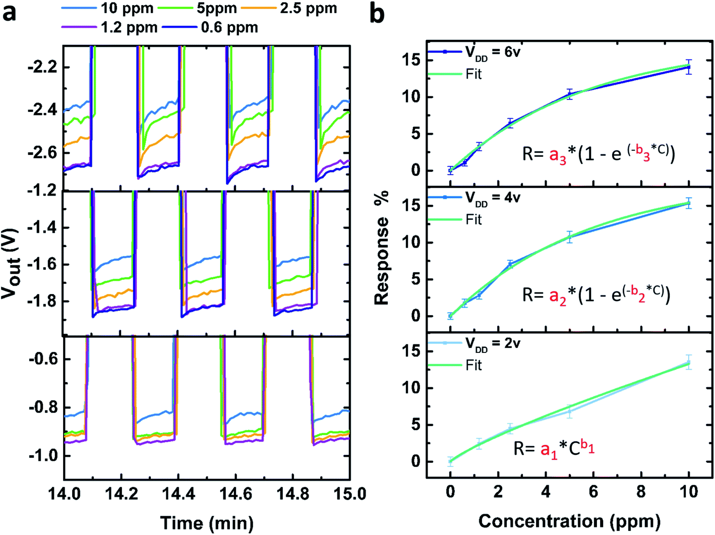 | ||
| Fig. 3 (a) Output voltage of the inverter after exposure to various concentrations of NO2 gas for a Vin at −4 V and −11 V alternatively for three different VDD values (from top to bottom: VDD = 6 V, 4 V and 2 V). (b) Response of the inverter as a function of NO2 concentration for the three different VDD values (from top to bottom: VDD = 6 V, 4 V and 2 V). | ||
These results are in agreement with previous results, where we showed that the particular design of our transistor device allows the detection of very low concentrations of gas.42 Nevertheless, it is important to highlight that adopting the inverter configuration slightly hinders the sensitivity of the device in comparison to our previously reported single SWCNTs-FET devices.42 However, the LOD for the inverted device is still reasonably comparable to other SWCNT-FET based gas sensors21,24,26,48–52 (see Table S4 in the ESI†). Moreover, the inverter configuration enables simpler data measurement and analysis, a possible miniaturization of the complete measurement chain of the sensor, and low power consumption. Then, for a further specific application a trade-off between the device ease of implementation has to be assessed against the sensitivity and LOD.
Following these results, we can safely claim that the use of an inverter configuration simplifies the sensing technology preserving the ability to detect low NO2 gas molecules concentrations.
In order to obtain a calibration curve of our device, we calculate the response for each concentration after a continuous exposure to NO2 for 15 min for three different VDD values.
The response (R) is defined by the following eqn (1):
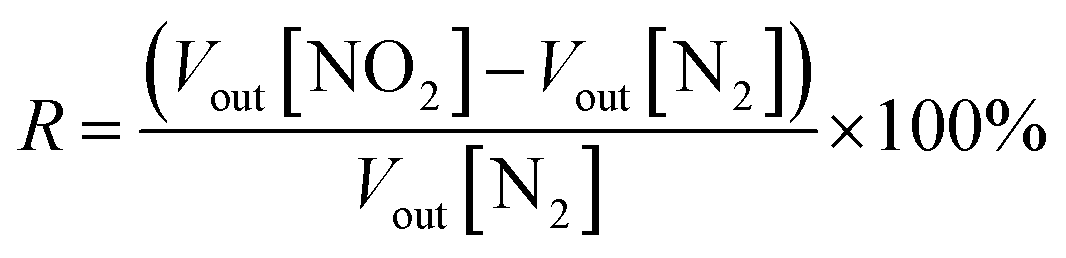 | (1) |
For both voltage values (Vout[N2] and Vout[NO2]), the error is defined as the standard deviation of the average, the error on the response is then calculated from those errors by propagation.
As shown on Fig. 3b, the logic inverter response (R) as a function of NO2 concentration (C) can be fit by a power law in the configuration VDD = 2 V, similar to other reported semiconductor based gas sensors that detect oxidizing gases,53 on the other hand, for VDD = 4 and 6 V an exponential relation was chosen as a much better fit was obtained using this function. The results of the different fits are detailed in Table 1.
| V DD (V) | a i | b i | r 2 |
|---|---|---|---|
| 2 (i = 1) | 1.974 ± 0.248 | 0.828 ± 0.0632 | 0.991 |
| 4 (i = 2) | 18.833 ± 1.626 | 0.170 ± 0.025 | 0.994 |
| 6 (i = 3) | 17.473 ± 1.968 | 0.173 ± 0.032 | 0.991 |
The LOD of the gas sensor device was also calculated for the three VDD used, and are presented in Table 2, the details of the calculation can be found in the ESI† (Section 7). As shown in Table 2 for VDD = 4 and 6 V, the obtained LODs are 0.57 ± 0.14 ppm and 0.56 ± 0.21 ppm, respectively while for VDD = 2 V a LOD of 0.92 ± 0.20 ppm is found. Then, for the detection of low concentrations, the inverter should be used at VDD = 4 V or 6 V where similarly low LODs were obtained.
| V DD (V) | LOD (ppm) | Error (ppm) |
|---|---|---|
| 2 | 0.92 | 0.20 |
| 4 | 0.57 | 0.14 |
| 6 | 0.56 | 0.21 |
According to the fits of the calibration curves shown in Fig. 3b for the three different working voltages, we expect rapidly occurring plateau for VDD = 4 V and VDD = 6 V (extrapolating the fits for these two curves leads to an asymptotic behaviour), whereas this is not the case for VDD = 2 V. Using the device at VDD = 2 V will therefore be more appropriate when detecting higher gas concentrations, however, further studies at higher concentrations must be performed to verify these assumptions.
Conclusions
To summarize, we have demonstrated that a CMOS inverter fabricated by associating a p-type SWCNT-FET with an n-type SWCNT-FET could be used as an efficient sensor for NO2 gas. The main advantage of the system relies on a huge simplification of the measuring system as a simple voltmeter can be used to detect the presence of gas, even for very small concentrations. We also showed that by changing the applied voltage VDD the sensitivity of the device can be tuned for measurement in different concentration ranges. Moreover, we show that a calibration of the device can be achieved, showing its potential for implementation in electronic readouts thanks to its compatibility with a further analog to digital conversion.This generic process could also be generalized to detect other gases using for instance functionalized SWCNTs in order to increase the specificity of the response. The introduced approach opens new frontiers in the SWCNT gas sensing field, the innovative core of the present work relies on simply measuring the output as a tension instead a low current. Moreover, here a logic inverter with two transistors has been explored, but the same principle can be expanded using a resistance device, or alternatively using other logic device configurations such as flip-flop memory cells or ring oscillators.35
Conflicts of interest
There are no conflicts to declare.Acknowledgements
The research leading to these results has received funding from the Chaire de Recherche PSA AC3M sponsored by Citroën at Ecole Polytechnique, Chaire EXXI sponsored by EDF at Ecole Polytechnique, the French state managed by the National Research Agency under the Investments for the Future program under the reference ANR-10-EQPX-0048. This work is part of the NanoMaDe-3E Initiative.Notes and references
- J. Zhang, X. Liu, G. Neri and N. Pinna, Adv. Mater., 2016, 28, 795–831 CrossRef CAS.
- J. Zhang, Z. Qin, D. Zeng and C. Xie, Phys. Chem. Chem. Phys., 2017, 19, 6313–6329 RSC.
- T. Wagner, S. Haffer, C. Weinberger, D. Klaus and M. Tiemann, Chem. Soc. Rev., 2013, 42, 4036–4053 RSC.
- P. T. Moseley, Meas. Sci. Technol., 2017, 28, 082001 CrossRef.
- M. M. Shulaker, G. Hills, R. S. Park, R. T. Howe, K. Saraswat, H.-S. P. Wong and S. Mitra, Nature, 2017, 547, 74–78 CrossRef CAS.
- S. Virji, J. Huang, R. B. Kaner and B. H. Weiller, Nano Lett., 2004, 4, 491–496 CrossRef CAS.
- S. Bai, C. Sun, P. Wan, C. Wang, R. Luo, Y. Li, J. Liu and X. Sun, Small, 2015, 11, 306–310 CrossRef CAS.
- H. Tang, Y. Li, R. Sokolovskij, L. Sacco, H. Zheng, H. Ye, H. Yu, X. Fan, H. Tian, T.-L. Ren and G. Zhang, ACS Appl. Mater. Interfaces, 2019, 11, 40850–40859 CrossRef CAS.
- Y. Yan, S. C. Warren, P. Fuller and B. A. Grzybowski, Nat. Nanotechnol., 2016, 11, 603–608 CrossRef CAS.
- A. Nag, A. Mitra and S. C. Mukhopadhyay, Sens. Actuators, A, 2018, 270, 177–194 CrossRef CAS.
- V. Schroeder, S. Savagatrup, M. He, S. Lin and T. M. Swager, Chem. Rev., 2019, 119, 599–663 CrossRef CAS.
- S. Srivastava, S. S. Sharma, S. Agrawal, S. Kumar, M. Singh and Y. K. Vijay, Synth. Met., 2010, 160, 529–534 CrossRef CAS.
- J. K. Abraham, B. Philip, A. Witchurch, V. K. Varadan and C. Channa Reddy, Smart Mater. Struct., 2004, 13, 1045–1049 CrossRef CAS.
- S. W. Lee, W. Lee, Y. Hong, G. Lee and D. S. Yoon, Sens. Actuators, B, 2018, 255, 1788–1804 CrossRef CAS.
- T. Chen, L. Wei, Z. Zhou, D. Shi, J. Wang, J. Zhao, Y. Yu, Y. Wang and Y. Zhang, Nanoscale Res. Lett., 2012, 7, 1 CrossRef.
- L. Valentini, I. Armentano, J. M. Kenny, C. Cantalini, L. Lozzi and S. Santucci, Appl. Phys. Lett., 2003, 82, 961–963 CrossRef CAS.
- I. Dube, D. Jiménez, G. Fedorov, A. Boyd, I. Gayduchenko, M. Paranjape and P. Barbara, Carbon, 2015, 87, 330–337 CrossRef CAS.
- Z. Li, J. Ding, C. Guo, J. Lefebvre and P. R. L. Malenfant, Adv. Funct. Mater., 2018, 28, 1–8 Search PubMed.
- G. Thangamani J., K. Deshmukh, K. Kumar Sadasivuni, K. Chidambaram, M. Basheer Ahamed, D. Ponnamma, M. Al-Ali AlMaadeed and S. K. Khadheer Pasha, Adv. Mater. Lett., 2017, 8, 196–205 CrossRef.
- A. Boyd, I. Dube, G. Fedorov, M. Paranjape and P. Barbara, Carbon, 2014, 69, 417–423 CrossRef CAS.
- J. Kong, N. R. Franklin, C. Zhou, M. G. Chapline, S. Peng, K. Cho and H. Dai, Science, 2000, 287, 622–625 CrossRef CAS.
- X. Liu, Z. Luo, S. Han, T. Tang, D. Zhang and C. Zhou, Appl. Phys. Lett., 2005, 86, 1–3 Search PubMed.
- E. S. Snow, F. K. Perkins and J. A. Robinson, Chem. Soc. Rev., 2006, 35, 790 RSC.
- M. Jeon, B. Choi, J. Yoon, D. M. Kim, D. H. Kim, I. Park and S.-J. Choi, Appl. Phys. Lett., 2017, 111, 022102 CrossRef.
- Y. H. Ngo, M. Brothers, J. A. Martin, C. C. Grigsby, K. Fullerton, R. R. Naik and S. S. Kim, ACS Omega, 2018, 3, 6230–6236 CrossRef CAS.
- X. Wang, M. Wei, X. Li, S. Shao, Y. Ren, W. Xu, M. Li, W. Liu, X. Liu and J. Zhao, ACS Appl. Mater. Interfaces, 2020, 12, 51797–51807 CrossRef CAS.
- P. Bondavalli, P. Legagneux and D. Pribat, Sens. Actuators, B, 2009, 140, 304–318 CrossRef CAS.
- P. Bondavalli, P. Legagneux, D. Pribat, A. Balan and S. Nazeer, J. Exp. Nanosci., 2008, 3, 347–356 CrossRef CAS.
- P. Avouris, Z. Chen and V. Perebeinos, Nat. Nanotechnol., 2007, 2, 605–615 CrossRef CAS.
- S.-H. Choi, S.-M. Yee, H.-J. Ji, J.-W. Choi, Y.-S. Cho and G.-T. Kim, Jpn. J. Appl. Phys., 2009, 48, 06FD13 Search PubMed.
- S. M. Mortazavi Zanjani, M. Holt, M. M. Sadeghi, S. Rahimi and D. Akinwande, npj 2D Mater. Appl., 2017, 1, 36 CrossRef.
- B. K. Crone, A. Dodabalapur, R. Sarpeshkar, A. Gelperin, H. E. Katz and Z. Bao, J. Appl. Phys., 2002, 91, 10140 CrossRef CAS.
- N. J. Tremblay, B. J. Jung, P. Breysse and H. E. Katz, Adv. Funct. Mater., 2011, 21, 4314–4319 CrossRef CAS.
- C. S. Cojocaru, B. Lebental, F. Z. Bouanis and E. Norman, Patent WO 2013144340 A1, 2013.
- A. Bachtold, P. Hadley, T. Nakanishi and C. Dekker, Science, 2001, 294, 1317–1320 CrossRef CAS.
- F. Zahoor, T. Z. A. Zulkifli, F. A. Khanday and S. A. Z. Murad, IEEE Access, 2020, 8, 104701–104717 Search PubMed.
- Z. Zhang, S. Wang, L. Ding, X. Liang, T. Pei, J. Shen, H. Xu, Q. Chen, R. Cui, Y. Li and L.-M. Peng, Nano Lett., 2008, 8, 3696–3701 CrossRef CAS.
- M. Ossaimee, N. Salem, M. Abouelatta and A. Shaker, ECS J. Solid State Sci. Technol., 2020, 9, 101002 CrossRef CAS.
- S. V. Bhole, U. S. Sonawane, C. K. Kasar and J. P. Bange, Study of Varying Tubes in Carbon Nanotube FET Based Inverter, in Recent Trends in Materials and Devices. Springer Proceedings in Physics, ed. V. Jain, S. Rattan and A. Verma, 2017, vol. 178, Springer, Cham, DOI:10.1007/978-3-319-29096-6_69.
- S. K. Sinha and S. Chaudhury, IEEE Trans. Nanotechnol., 2013, 12, 958–964 CAS.
- N. S. Suhaimi and H. Hussin, ECS J. Solid State Sci. Technol., 2020, 9, 41003 CrossRef CAS.
- L. Sacco, S. Forel, I. Florea and C. Cojocaru, Carbon, 2020, 157, 631–639 CrossRef CAS.
- A. Castan, S. Forel, L. Catala, I. Florea, F. Fossard, F. Bouanis, A. Andrieux-Ledier, S. Mazerat, T. Mallah, V. Huc, A. Loiseau and C. S. Cojocaru, Carbon, 2017, 123, 583–592 CrossRef CAS.
- S. Forel, A. Castan, H. Amara, I. Florea, F. Fossard, L. Catala, C. Bichara, T. Mallah, V. Huc, A. Loiseau and C.-S. Cojocaru, Nanoscale, 2019, 11, 4091–4100 RSC.
- M. Shim, A. Javey, N. W. S. Kam and H. Dai, J. Am. Chem. Soc., 2001, 123, 11512–11513 CrossRef CAS.
- S. Santra, S. Z. Ali, P. K. Guha, G. Zhong, J. Robertson, J. A. Covington, W. I. Milne, J. W. Gardner and F. Udrea, Nanotechnology, 2010, 21, 485301 CrossRef.
- R. J. Chen, N. R. Franklin, J. Kong, J. Cao, T. W. Tombler, Y. Zhang and H. Dai, Appl. Phys. Lett., 2001, 79, 2258–2260 CrossRef CAS.
- M. Lucci, A. Reale, A. Di Carlo, S. Orlanducci, E. Tamburri, M. L. Terranova, I. Davoli, C. Di Natale, A. D'Amico and R. Paolesse, Sens. Actuators, B, 2006, 118, 226–231 CrossRef CAS.
- K. Chikkadi, M. Muoth, W. Liu, V. Maiwald and C. Hierold, Sens. Actuators, B, 2014, 196, 682–690 CrossRef CAS.
- J. Li, Y. Lu, Q. Ye, M. Cinke, J. Han and M. Meyyappan, Nano Lett., 2003, 3, 929–933 CrossRef CAS.
- S. Wang, Z. Zhang, L. Ding, X. Liang, J. Shen, H. Xu, Q. Chen, R. L. Cui, Y. Li and L. M. Peng, Adv. Mater., 2008, 20, 3258–3262 CrossRef CAS.
- K. Xu, C. Wu, X. Tian, J. Liu, M. Li, Y. Zhang and Z. Dong, Integr. Ferroelectr., 2012, 135, 132–137 CrossRef CAS.
- N. Yamazoe and K. Shimanoe, Sens. Actuators, B, 2008, 128, 566–573 CrossRef CAS.
Footnotes |
| † Electronic supplementary information (ESI) available. See DOI: 10.1039/d0na00811g |
| ‡ These authors contributed equally. |
| § Present address: Antwerp University, Physics Department, Experimental Condensed Matter Physics Laboratory, Universiteitsplein 1, 2610 Antwerp, Belgium. Email: E-mail: salome.forel@uantwerpen.be |
| ¶ Present address: Delft University of Technology, Faculty of Electrical Engineering, Mathematics and Computer Science, Department of Microelectronics, Delft, Feldmannweg 17, 2628 CT Delft, Netherlands. Email: E-mail: l.n.sacco@tudelft.nl |
| || Present address: Department of Physics and Astronomy, University of Pennsylvania, Philadelphia PA 19104, USA. |
| This journal is © The Royal Society of Chemistry 2021 |