DOI:
10.1039/D0NA00787K
(Paper)
Nanoscale Adv., 2021,
3, 1758-1766
A reconfigurable hyperbolic metamaterial perfect absorber†
Received
23rd September 2020
, Accepted 29th January 2021
First published on 1st February 2021
Abstract
Metamaterial (MM) perfect absorbers are realised over various spectra from visible to microwave. Recently, different approaches have been explored to integrate tunability into MM absorbers. Particularly, tuning has been illustrated through electrical-, thermal-, and photo-induced changes to the permittivity of the active medium within MM absorbers. However, the intricate design, expensive nanofabrication process, and the volatile nature of the active medium limit the widespread applications of MM absorbers. Metal–dielectric stack layered hyperbolic metamaterials (HMMs) have recently attracted much attention due to their extraordinary optical properties and rather simple design. Herein, we experimentally realised a reconfigurable HMM perfect absorber based on alternating gold (Au) and Ge2Sb2Te5 (GST225) layers for the near-infrared (N-IR) region. It shows that a red-shift of 500 nm of the absorptance peak can be obtained by changing the GST225 state from amorphous to crystalline. The nearly perfect absorptance is omnidirectional and polarisation-independent. Additionally, the absorptance peak can be reversibly switched in just five nanoseconds by re-amorphising the GST225, enabling a dynamically reconfigurable HMM absorber. Experimental data are validated numerically using the finite-difference time-domain method. The absorber fabricated using our strategy has advantages of being reconfigurable, uncomplicated, and lithography-free over conventional MM absorbers, which may open up a new path for applications in energy harvesting, photodetectors, biochemical sensing, and thermal camouflage techniques.
1. Introduction
Perfect absorption achieved by photonic devices is promising for many applications such as energy harvesting, radiative cooling, thermal emitters, photodetectors, solar cells, thermal imaging, optical modulators, and colour filters.1–19 Recently, metamaterial (MM) perfect absorbers have been demonstrated in the spectra ranging from visible to GHz.20–28 By adjusting the resonances in the effective permittivity and permeability independently, one can match the impedance of MMs to that of free-space to obtain a high absorption. Nevertheless, some disadvantages hold back the commercial potential of MM absorbers. For example, the subwavelength-scale meta-atom needs to be fabricated using top-down lithography techniques i.e., focused ion beam (FIB) milling or electron-beam lithography (EBL). Those techniques have restricted spatial resolution and are very hard to scale up to large-field patterning; moreover, since they are serial writing techniques, the fabrication throughput is low. To solve the problem, recently a few remarkable techniques have been developed to fabricate large-size MMs while having a low-cost, including nano-printing, interference lithography, etc.29–31
Alternatively, metal/dielectric stacks, so-called hyperbolic metamaterials (HMMs), have recently witnessed an exponentially increasing interest, featured by the unique property of their permittivity tensors in which the signs of diagonal components are different.32 Specifically, photonic HMMs are uniaxial nanocomposite structures based on the permittivity tensor of the diagonal expression [ε] = diag(ε‖, ε‖, ε⊥). The principal elements have the opposite signs ε‖ > 0, ε⊥ < 0 (type-I) and ε‖ < 0, ε⊥ > 0 (type-II).33 This leads to a hyperbolic-type surface of dispersion in wavevector space, defined as hyperbolic dispersion. Unlike MMs composed of subwavelength resonator arrays, HMMs exhibiting a nominally infinite density of states34 can support EM-waves with a high propagation wave-vector while not requiring periodicity in the plane normal to the incident wave and can be fabricated using conventional thin film sputtering. Therefore, they are considered appropriate for bulky-area surfaces, enabling them to be practical for applications such as super-resolution imaging,35,36 resonant gain singularities,37 light beam steering,38,39 spontaneous emission enhancement,40 super-collimation,41 ultra-sensitive biosensors,42,43 negative refraction,44 and near-zero epsilon.45 Such unique properties have enabled HMMs to be widely exploited for absorption application.46
Recently, Sreekanth et al. proposed a type-II (Ag/TiO2) HMM structure for multiband perfect absorption in the near-infrared (N-IR) region.47 A wide-angle ultra-broadband infrared (IR) absorber was demonstrated by Cui et al. using Ge/Au sawtoothed anisotropic MMs.48 More recently, Lin et al. demonstrated a broadband perfect absorber of graphene-based HMMs.49 Desouky et al. theoretically demonstrated a super absorber in the mid-infrared (M-IR) spectral range using silicon and doped silicon-based HMMs.50 Nevertheless, the current HMM absorbers are limited to a fixed spectral region. It is because the extreme anisotropy and hyperbolic dispersion of HMMs are determined by their metal and dielectric constituents and the filling fraction, which are fixed after the fabrication.
On the other hand, different methods have been exploited to integrate tunability into HMMs, where the tunability is demonstrated through stimulus sensitive functional dielectrics, i.e., conductive oxides,51 liquid crystals,52 gyromagnetics,53 or semiconductors.54 It allows for active control of HMM properties by photo-, electrical-, and thermal-induced variations to the permittivity of the active dielectric within the HMM structure. Yet, so far rare efforts have been made to obtain a reversibly tunable HMM absorber. There are, however, loads of applications where a reconfigurable light absorption is highly wanted. For example, a switchable perfect absorber can find important applications in electro-optic switches,55 selective thermal emitters,56 and tunable sensors.57 Furthermore, in HMM absorbers the dielectric components are passive (i.e., SiO2 and TiO2), which does not change the absorbed photons into electron–hole pairs. This forbids their applications for photodetectors and photovoltaic cells. These issues motivate our study, in which we look into actively reconfigurable HMM perfect absorbers over genuinely macroscopic size via a scalable, straightforward, and low-cost fabrication procedure.
The family of chalcogenide semiconductors of the Ge–Sb–Te (GST) phase-change material (PCM) exhibits two stable structural states: amorphous and crystalline. GST can undergo a reversible structural transition, leading to a substantial change in its optical and electrical properties. Such a unique characteristic enables them to be suitable for photonics applications, ranging from multilevel storage and displays to integrated nanophotonic systems.58 Due to its prompt state transition, high cyclability, and outstanding thermal stability, GST is important for high-speed and switchable photonic devices.59–61 For example, tunable negative index metamaterials,62 rewritable metasurface lenses,63 thermal emitters,56 beam steering64,65 and tunable chirality66,67 have been explored. Recently, GST has been demonstrated as a promising candidate functional dielectric to perform as a tunable metasurface perfect absorber in the mid-infrared (M-IR) spectrum.11 Nevertheless, this tuning strategy turns out to be unrealistic for the N-IR spectrum. It is because the fabrication of periodic nanoantenna arrays working in the N-IR region needs either FIB or EBL patterning, which is high-cost and time-consuming. The N-IR spectrum is, however, a technologically key spectrum with highly significant applications like molecular sensing and optical telecommunications.68
In this work, we demonstrate a tunable HMM perfect absorber based on bilayer stacks consisting of alternating gold (Au) and a prototypical PCM, Ge2Sb2Te5 (GST225) of subwavelength thickness. A non-volatile ultrafast reconfigurable HMM perfect absorber is experimentally obtained by exploring the reversible amorphous-to-crystalline state change of GST225. The HMM structure maintains an omnidirectional perfect absorption for both p- and s-polarisations and shows type-II hyperbolic dispersion over the N-IR region. A numerical simulation based on the finite-difference time-domain (FDTD) method is performed to investigate the physics underlying the high absorption. Compared with the previous light absorber consisting of nanoantenna arrays fabricated by the top-down method, our HMM perfect absorber does not need lithographic patterning that results in advantages of scalability, low-cost, macroscopic scale and high throughput. For this work, the GST alloy is chosen as the functional material because not only its optical properties undergo a radical change during the amorphous–crystalline phase change, but also it is an active semiconductor that can convert the absorbed light energy into electron–hole pairs,69 making the GST225 based HMM absorber useful for photodetectors or photovoltaic cells. Another key advantage of the reconfigurable HMM absorber is its non-volatile feature since the energy is only needed for the phase changing process and not for keeping a particular structural phase. Therefore, once the HMM absorber is transited, it will maintain its optical properties until it is transited again. This certainly enables HMM absorbers to be appealing from a green technology outlook. We propose that this large-area, omnidirectional, polarisation-insensitive and reconfigurable HMM absorber can be a promising candidate for energy harvesting, bio-chemical sensing, thermal emitters, photodetectors, and thermal camouflage techniques. The lithography-free and high throughput fabrication process may lead to absorption- and emissivity-controllable surfaces with arbitrary size.
2. Results and discussion
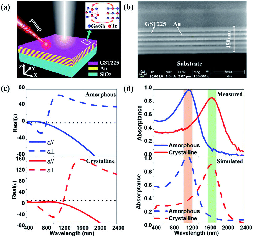
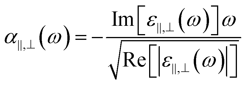
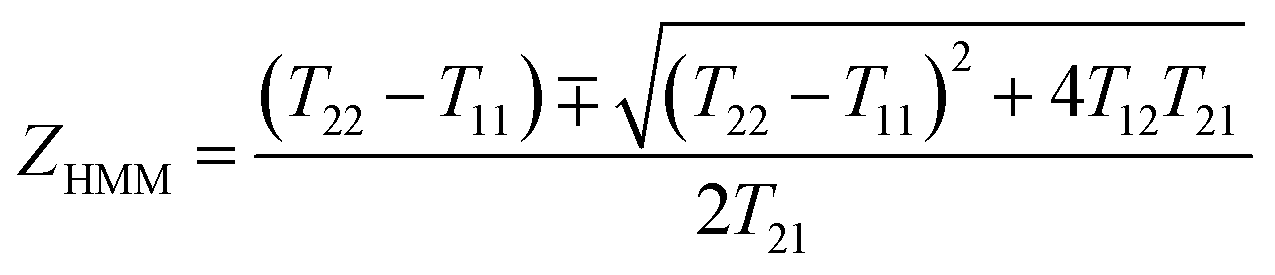
Fig. 1(a) schematically illustrates a reconfigurable HMM perfect absorber composed of Au–GST225 stacked layers, where a non-volatile bidirectional switching functionality can be realised via a reversible phase transition. The perfect absorber is a type-II HMM consisting of six periods of alternating planar films of 40 nm thick GST225 and Au. The HMM is fabricated on the fused silica (SiO2) substrate by using physical vapour deposition (see Methods for details). A second electron microscopy (SEM) cross-section of the HMM (Fig. 1(b)) can be used to distinguish each GST225 and Au film. It confirms that no diffusion occurs during the layer deposition. The HMM absorber is experimentally measured using variable angle spectroscopic ellipsometry (VASE) over a wide spectral range of 400–2400 nm. The measured data are analysed by employing a uniaxial anisotropy model46,70,71 to extract the effective out-of-plane (ε⊥) and in-plane (ε‖) permittivity of the HMM absorber. Particularly, the ε‖ and ε⊥ are obtained via72,73| | | ε‖ = f × εAu + (1 − f) × εGST | (1) |
| | | ε⊥ = (εAu × εGST)/(f × εGST + (1 − f) × εAu) | (2) |
where εGST and εAu are the permittivity of the GST225 and Au, respectively, f = tAu/(tAu + tGST) the filling fraction, and tAu and tGST the thickness of the Au and the GST225 layer, respectively. The εGST values for both amorphous (ESI Fig. S1(a)†) and crystalline (ESI Fig. S1(b)†) states are measured using the VASE, respectively, which are fitted using the Tauc–Lorentz model. A Drude model is used to fit the measured εAu (ESI Fig. S1(c)†).74 The top panel of Fig. 1(c) presents the measured real parts of ε⊥ and ε‖ of the HMM absorber for the as-deposited (AD) amorphous (AM) state. As is seen, the AD-AM HMM possesses the hyperbolic dispersions of type-I (real(ε‖) > 0, real(ε⊥) < 0) and type-II (real(ε‖) < 0, real(ε⊥) > 0) in the visible (λ < 700 nm) and N-IR (λ > 840 nm) regions, respectively. Afterwards, the HMM absorber is annealed at Tg = 200 °C in an argon atmosphere for 30 min. Such a temperature is above the crystallisation point of Tc = 160 °C but below the melting point of Tm = 630 °C,61 which can change the structural state from amorphous to crystalline (CR). In the bottom panel, we show the real(ε‖) and real(ε⊥) of the annealed HMM absorber extracted from the VASE measurement. The type-II hyperbolic dispersion in the N-IR region is redshifted (λ > 1200 nm) by crystallising the absorber. The crystallised HMM absorber, however no longer exhibits type-I hyperbolic dispersion in the visible region. The large variation in εGST between the amorphous and crystalline structural phases (see ESI Fig. S1(a and b)†) engineers the optical transition matrix elements, that in turn, tunes the hyperbolic dispersion.
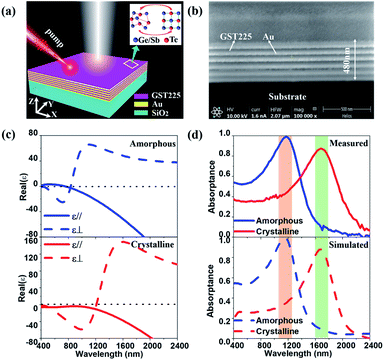 |
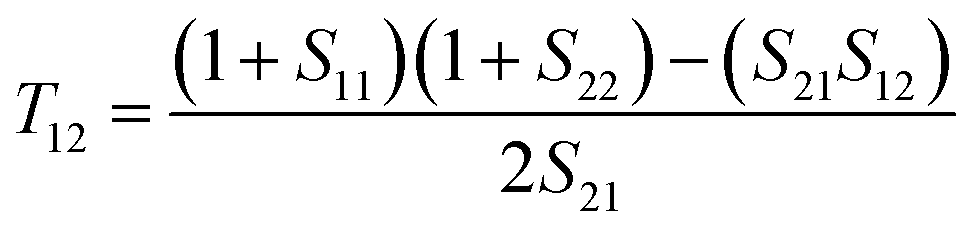
| | Fig. 1 (a) Scheme of the reconfigurable phase-change HMM absorber, where the structure is composed of Au–GST225 stacked layers. Both the GST225 and Au films have an identical thickness of 40 nm. The whole HMM absorber sits on a silica substrate. (b) FIB image of the cross-section of the HMM absorber. (c) Real parts of the ε‖ and ε⊥ of the HMM absorber extracted from VASE as transiting the GST225 state from amorphous (top panel) to crystalline (bottom panel). (d) The VASE measured (top panel) and FDTD simulated (bottom panel) A(ω) of the HMM absorber for the amorphous and crystalline states. | |
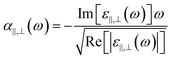
The reflectance (R(ω)) and transmittance (T(ω)) spectra of the HMM absorber are directly measured using VASE (see Methods for details). The absorptance is derived from A(ω) = 1 − R(ω) − T(ω). The absorber possesses a zero transmittance that can simplify the absorptance to A(ω) = 1 − R(ω). In the top panel of Fig. 1(d), we first measure the A(ω) for both amorphous (blue solid line) and crystalline (red solid line) states. The chalcogenide HMM absorber possesses a nearly perfect absorptance in the N-IR region, with a peak absorptance of A(ω) = 0.99 at the resonant wavelength of λa = 1180 nm for the amorphous phase. As transiting the structural state from amorphous to crystalline, peak A(ω) undergoes a radical redshift of 500 nm, while maintaining a high absorptance of A(ω) = 0.86 at the resonant wavelength of λc = 1680 nm, permitting switching between two distinct spectra. Due to the widely spectral shift, our HMM absorber has a significant A(ω) contrast of ΔA(ω) = 0.78 at λc = 1680 nm. The numerically calculated HMM absorber A(ω) spectra agree with experimentally measured spectra. In the bottom panel, we have simulated the A(ω) spectra of the HMM absorber using the finite different time domain (FDTD) solver within Lumerical Solution.75 The HMM absorber is simulated with normal plane wave illumination, and the wave vector points towards the −z axis. The HMM geometry is set to those measured using the FIB cross-section image presented in Fig. 1(b). A detailed description of the numerical model can be found in the Method. The numerical calculation validates the spectral moving direction by changing the structural phase; it demonstrates that the theoretical A(ω) has a good agreement with the experimental A(ω). To simplify the numerical model, the surface roughness and fabrication defects are not considered. Such a simplification induces variations between the simulated and measured A(ω), as well as slight widening of the measured resonances. Moreover, the A(ω) spectra are measured in the far-field. However, in the model the A(ω) spectra are calculated in the near-field of the HMM absorber, which also causes variations between the calculation and measurement. The effective absorption for the light transmitting in the HMM absorber can be expressed as
| |  | (3) |
where
α‖(
ω) and
α⊥(
ω) present effective absorption produced by beams transmitting along the
z-axis and in the “
x–
y” plane, respectively.
76 Therefore, the absorption is dependent on the
ε‖,⊥(
ω) having hyperbolic dispersion as shown in
Fig. 1(c). To exploit the underlying mechanism of the tunable perfect absorption, it is instructive to study the effective impedance of the HMM absorber,
77,78| | 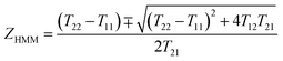 | (4) |
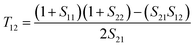
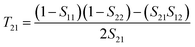
where the transfer (
T) matrix elements of
T11,
T12,
T21, and
T22 can be expressed by
| |  | (5) |
| |  | (6) |
| |  | (7) |
| |  | (8) |
where the
S11,
S12,
S21, and
S22 (scattering matrix (
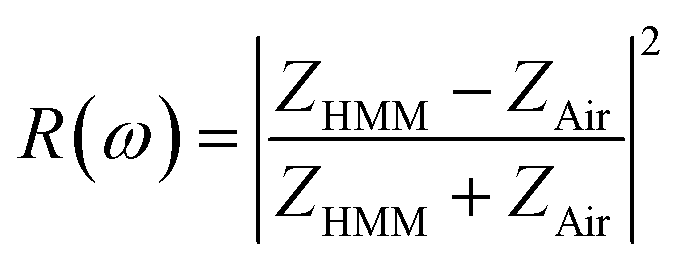
S) elements) are the scattering parameters of the reflectance and transmittance coefficient along the forward and backward directions, respectively. Moreover, according to Fresnel's equation, under a normal incidence, the reflectance of the HMM structure is defined as,
79| |  | (9) |
where
ZAir = 1 is the impedance of free-space. A perfect absorptance can be achieved when the impedance of the HMM absorber (
ZHMM) matches the free space (
ZAir = 1).
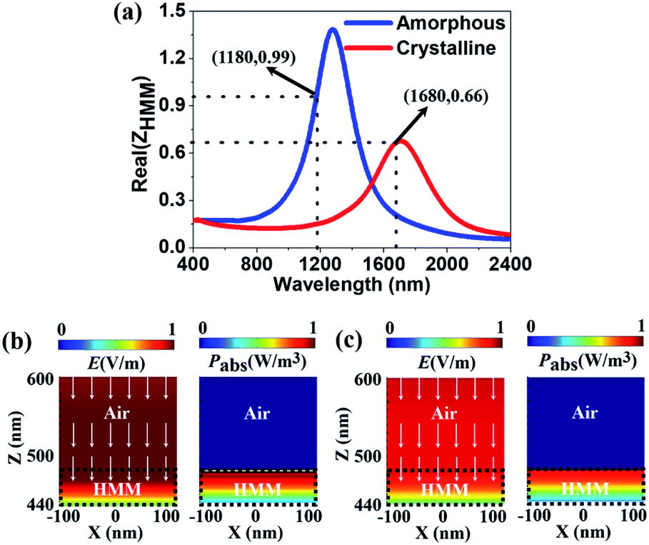
Fig. 2(a) shows the real part of the
ZHMM of the HMM absorber for the amorphous (blue solid line) and crystalline states (red solid line). For the amorphous state, the
ZHMM is nearly unity at the resonant wavelength of
λa = 1180 nm, leading to the perfect absorptance (
A(
ω) = 0.99). However, for the crystalline state the
ZHMM is decreased to 0.66 at the resonant wavelength of
λc = 1680 nm that breaks the impedance match. Thus, a lower absorptance of
A(
ω) = 0.86 occurs at
λc = 1680 nm for the crystalline state.
Fig. 2(b and c) show the FDTD simulated total electric (
E-) field intensity and absorbed power (
Pabs) distributions at
λa = 1180 nm for the amorphous state and
λc = 1680 nm for the crystalline state. In the pattern along the
x–
z plane, the white arrows represent the Poynting vector (
Sp) whereas the color represents the magnitudes of the
E-field intensity and power absorptance. The total
E-field intensity distribution |
E|
2 = |
Ex|
2 + |
Ey|
2 + |
Ez|
2 relating to
A(
ω) = 0.99 at
λa = 1180 nm for the amorphous state is presented in the left column of
Fig. 2(b). It clearly shows that the
E-field can be well concentrated inside the HMM absorber while gradually attenuating along the
z-direction. The power absorptance is expressed by
Pabs = 0.5
ω|
E|
2εim and
εim is the imaginary part of the permittivity.
80–82 As seen in the right column, the HMM can perfectly absorb the light although the
Pabs gradually decays along the
z-direction. Such a high absorptance is caused by the impedance match between the HMM and air for the amorphous state. In
Fig. 2(c), we illustrate the
E-field intensity (left column) and
Pabs (right column) relating to
A(
ω) = 0.86 at
λc = 1680 nm for the crystalline state. It shows that the field patterns of the structure are very similar to the ones for the amorphous phase, which indicates that the HMM also possesses high absorptance after crystallising the GST225 films. The
E-field intensity and
Pabs in the HMM with amorphous GST225 (
Fig. 2(b)) are stronger than for the crystalline phase (
Fig. 2(c)), implying that a higher absorptance (better impedance match) can be achieved.
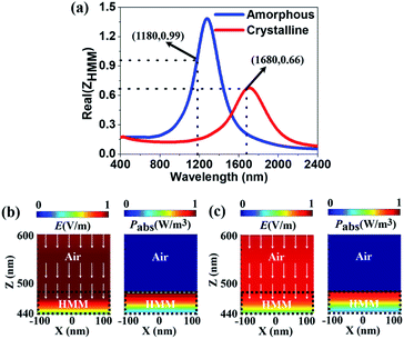 |
| | Fig. 2 (a) Effective impedance of the HMM absorber for both the amorphous (blue line) and crystalline (red line) states. (b and c) E-field intensity (left column) and absorbed power (right column) distributions of the HMM absorber for (b) the amorphous state at λa = 1180 nm, and (c) the crystalline state at λc = 1680 nm. The white arrows represent the Poynting vectors. The different regions of air and HMM are circled by the black dotted line. | |
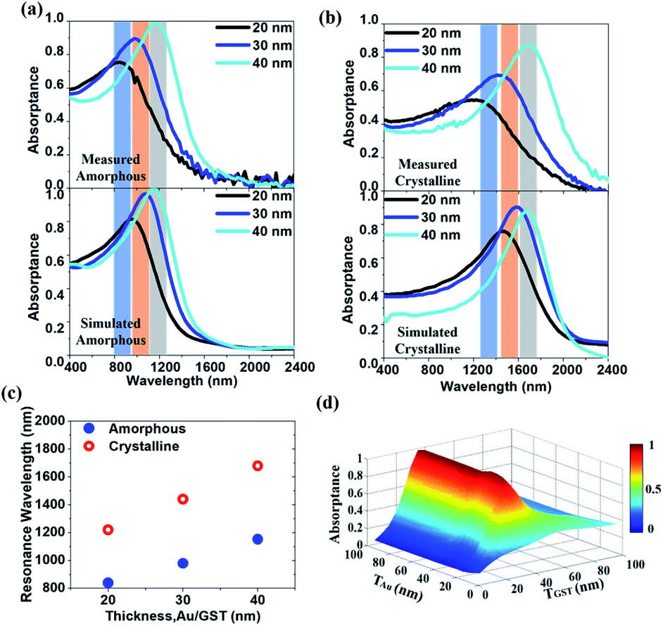
The A(ω) spectra resonant wavelength can be tuned by varying the thickness of constituent layers. We fabricate a series of HMM absorbers with the thickness of the Au (TAu) and GST225 (TGST) layers changing from 20 to 40 nm, while fixing the filling factor at f = 0.5 (namely, TAu = TGST). In the top panel of Fig. 3(a), we experimentally illustrate the A(ω) of the amorphous HMM absorber for various thicknesses. As is observed, the resonant peak redshifts across the N-IR spectral range with increasing the thickness of constituent layers. Integrating this absorber into N-IR photonic devices can resolve a particular spectral band. Furthermore, those resonances can be switched by crystallising the GST225, as shown in the top panel of Fig. 3(b). The FDTD simulated A(ω) spectra match well the measured ones. The bottom panels of Fig. 3(a and b) show the comparison. A redshift in the resonant peak is observed by either increasing the layer thickness or crystallizing the GST225. In Fig. 3(c), we experimentally present how the resonant wavelength can be switched by combining both variations in the layer thickness and the structural phase of GST225. Such an ability to cover a large part of the N-IR spectrum by simply changing the thickness of constituent layers and crystallising the GST225 makes it essential to use a micrometer-size N-IR hyperspectral imaging camera. In Fig. 3(d), for the amorphous HMM absorber we have numerically demonstrated a 2D diagram of absorptance against TAu and TGST with a step of 0.5 nm at a fixed wavelength of λa = 1180 nm. As can be seen, the absorptance achieves the highest value of 0.99 at λa = 1180 nm for TAu = TGST = 40 nm.
 |
| | Fig. 3 (a and b) The performance of resonance switching in the HMM absorber: VASE measured (top panels) and FDTD simulated (bottom panels) absorptance spectra for the (a) amorphous and (b) crystalline states. The filling factor is f = 0.5 and the thickness of the constituent layer is TAu = TGST = 20 nm (black lines), 30 nm (blue lines), and 40 nm (cyan lines), respectively. The redshift of the absorptance spectra can be both experimentally and numerically found by changing the GST225 state from amorphous to crystalline. (c) The resonant wavelength is plotted against the thickness of constituent layers for both the amorphous (blue dot) and crystalline (red open circle) phases. (d) A 2D diagram of absorptance against TAu and TGST at a fixed wavelength of λa = 1180 nm. | |
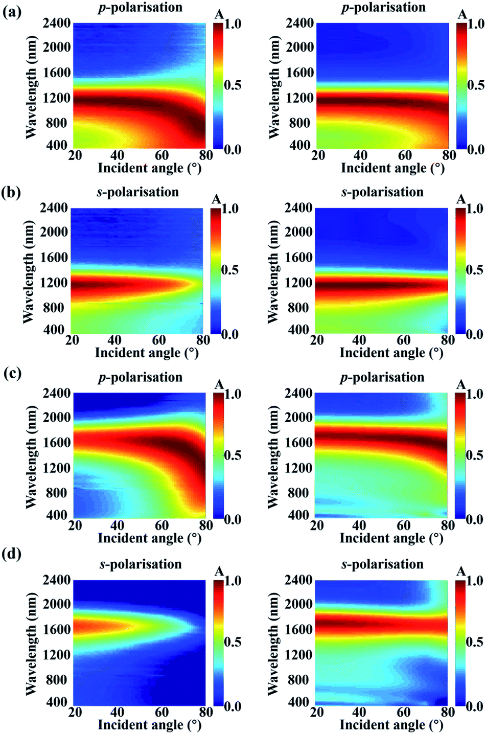
Ideal thermal photovoltaics, photon detectors, and emitters are desired to absorb incident light perfectly under full incident angles regardless of polarisation. For our proposed HMM perfect absorber, the absorptance is also robust under oblique incident angles (θi) for both the p- and s-polarisations. Fig. 4 shows the measured (left column) and simulated (right column) A(ω) spectra as the θi increases from 20° to 80° in a 2° step, where Fig. 4(a and b) present the A(ω) for the p- and s-polarisations in the amorphous state, respectively, Fig. 4(c and d) present the A(ω) for the p- and s-polarisations in the crystalline state, respectively. For the amorphous state, the A(ω) is maintained above 85% for θi < 50° from 1000 to 1250 nm under both p- and s-polarised incidences. Although the performance of the angular independent absorptance gets worse as transiting the GST structural state from amorphous to crystalline, there is a good spectral overlap between the A(ω) for p- and s-polarisations in each structural state. Therefore, the A(ω) of the HMM is not only omnidirectional but polarisation independent. There is a difference between the measured and simulated absorptance. This may stem from scattering of radiation from imperfections of fabrication.83 In the numerical model, a few factors are not considered, for example, the thickness of the native oxide layer, uncertainty in the incident angle, imperfections of fabrication, surface roughness, and grain boundaries. Such a simplification induces the observed discrepancy between the simulated and measured reflectance spectra. Meanwhile, the error in layer thickness monitoring in the deposition process may also cause the difference. Moreover, the reflectance was measured in the far-field via a focusing probe with ∼0.01 NA. Yet, in the model, the reflectance was recorded by the power monitor positioned above the HMM absorber, causing the differences between the experiment and simulation.
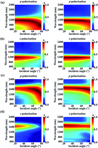 |
| | Fig. 4 The VASE measurement (left column) and FDTD simulation (right column) of incident angular-dependent absorptance spectra for the phase change HMM absorber on a SiO2 substrate under the illumination of (a) p- and (b) s-polarized lights for the amorphous state and (c) p- and (d) s-polarized lights for the crystalline state. | |
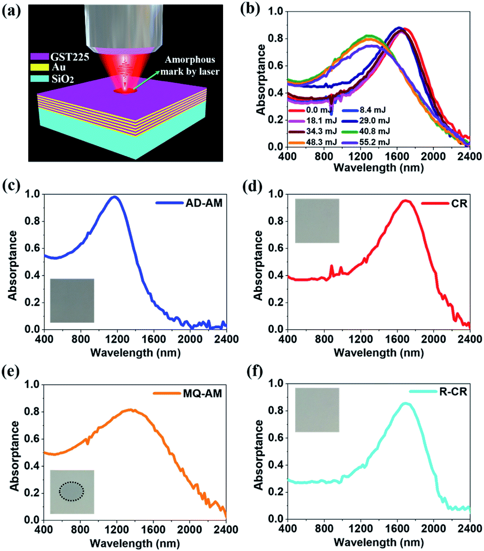
The GST225 film can be reliably switched more than 108 cycles between the amorphous and crystalline phases,84,85 which is a key advantage for reconfigurable photonic devices. This can enable various functionalities in the same photonic structure without changing its geometry. In this work, the reversible transition between the amorphous and crystalline phases results in a huge alteration in the complex permittivity εGST = real(εGST) + imag(εGST) × i (see ESI Fig. S1†), leading to a reversible tuning of the resonant frequency of peak absorptance. In ESI Fig. S2,† we schematically illustrate the treatment of the phase change HMM absorber. First, the as-deposited amorphous (AD-AM) HMM absorber is crystallised by thermally heating the structure for 30 min at Tg = 200 °C on a Linkam hotplate in a flowing argon atmosphere. To reversibly change the GST225 state from crystalline (CR) to melt quenched amorphous (MQ-AM), the crystal lattice has to be melt and quenched promptly at a rate of 109 to 1010 K s−1 to freeze the Ge, Sb, and Te atoms in the random position to form the disorder MQ-AM state.86 A single 5 nanosecond (ns) laser pulse can produce the sufficient energy to increase the local temperature momentarily above Tm = 630 °C to melt the GST225. The subsequent prompt cooling quenches the melted layer into the AM phase. Finally, to recrystallise (R-CR) the HMM with the MQ-AM GST225, the hot plate is employed to maintain the HMM above Tc = 160 °C but below Tm = 630 °C. A phase transition cycle of crystallisation (AD-AM → CR), reamorphisation (CR → MQ-AM), and recrystallisation (MQ-AM → R-CR) takes place at different temperatures and time scales. The reversible optical switching (namely, an amorphisation of GST225) is experimentally triggered by irradiating the sample with ns laser pulses.87
As schematically shown in Fig. 5(a), a home-built laser system consisting of a Q-switch pulsed laser (Quintel, Q-smart 850) operating at λ = 1064 nm, 5 ns pulse duration with a 10 Hz repetition rate is employed to amorphise the HMM absorber. The maximum output energy of the laser pulse is 850 mJ with a circular beam radius of 5 mm. To optimise the switching energy, a few laser amorphised marks (grey area circled by the white dashed line) are fabricated on the sample surface by using different laser energies. These marks are made on various areas by moving the sample via the translation stage. Fig. 5(b) shows the measured A(ω) spectra at the different marks. Initially, the HMM absorber with crystalline GST225 has a peak absorptance of A(ω) = 0.86 at λc = 1680 nm (red line). As increasing the laser energy from 0 mJ to 34.3 mJ, the A(ω) spectrum does not significantly change, indicating that the HMM structure is not yet amorphised. By increasing the energy to 40.8 mJ, the resonant peak massively blue shifts to λm = 1280 nm. However for the energy above 40.8 mJ, the resonant wavelength no longer shifts while the ablation effect slightly reduces the peak absorptance.88,89 Thus, the laser switching energy of 40.8 mJ is employed to amorphise the HMM absorber. In Fig. 5(c–f), we present experimentally a phase change HMM absorber operating in the N-IR region using a reversible phase transition of GST225 between the amorphous and crystalline states. The A(ω) spectra of the HMM absorber measured at the four structural states of AD-AM (blue line), hot plate annealed CR (red line), ns laser-induced MQ-AM (orange line), and hot plate annealed R-CR (cyan line) are presented, respectively. The resonant wavelength of the HMM absorber can redshift from λa = 1180 to λc = 1680 nm as transiting the structural state from AD-AM (Fig. 5(c)) to CR (Fig. 5(d)). The CR-HMM is subsequently reamorphised to the MQ-AM state (Fig. 5(e)), leading to a blueshift of the resonant wavelength from λc = 1680 nm to λMQ = 1280 nm. The MQ-AM HMM can be fully recrystallised to move the resonant wavelength from λMQ = 1280 nm to λRC = 1680 nm (Fig. 5(f)). The insets show the microscopy images of the HMM absorber at the various states, accordingly. The CR-HMM appears (Fig. 5(d)) to be brighter than AM-HMM (Fig. 5(c)) due to a decreasing absorptance after crystallisation. The MQ-AM HMM can change back to a dark color (circled by a dotted line in Fig. 5(e)), indicating an increasing absorptance. The restored, recrystallized HMM (Fig. 5(f)) has a similar color to that crystallised in the first writing. Although the resonant wavelength of the CR-HMM (λc = 1680 nm) perfectly matches that of the R-CR HMM (λRC = 1680 nm), a difference occurs in the resonant wavelengths between the AD-AM (λa = 1180 nm) and MQ-AM (λMQ = 1280 nm) states. It is because that the optical and structural properties of the as-deposited (AD) amorphous (AM) phase are slightly different than those of the melt-quenched (MQ) amorphous (AM) state. A detailed comparison can be found in the ESI of ref. 90. The laser induced amorphization (MQ-AM) is not sufficient to cause a complete reversion to the AD-AM state, and there are different crystallisation kinetics between the AD-AM and MQ-AM structural states.88,91,92 Indeed, the MQ-AM state is intermediate in structure between the AD-AM and CR phases. As seen in Fig. 5(c–e), the absorptance spectrum of HMM for the MQ-AM state is located between the spectra of the AD-AM and CR samples. The reconfigurable absorptance control and dynamic band-selectivity in the HMM absorber offer a main advantage over the previous light absorber, not to mention its potential to convert the absorbed light energy into electron–hole pairs. In ESI Fig. S3,† we numerically studied the effect of the layer period (P) on the absorptance using Lumerical solution. We find that the peak absorptance for the HMM absorber with the amorphous state becomes higher as increasing P from 4 to 6 while maintaining the peak value around 1182 nm when P > 6. This indicates that layers of period of 6 (P = 6) can be seen as an effective material.
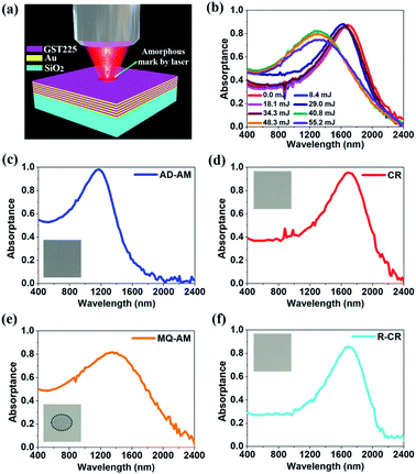 |
| | Fig. 5 (a) Schematic illustration of the laser amorphised mark on the CR-HMM. (b) Absorptance spectra of the CR-HMM under the various laser energies of 0, 8.4, 18.1, 29.0, 34.3, 40.8, 48.3, and 55.2 mJ. (c–f) The absorptance spectra of the phase change HMM absorber with the different phases of (c) AD-AM, (d) CR, (e) MQ-AM, and (f) R-CR, where the insets are the microscope images of the HMM absorber. | |
3. Conclusions
In conclusion, we both experimentally and theoretically demonstrate a versatile platform for achieving reconfigurable, polarisation-independent, and omnidirectional near-perfect light absorption across the N-IR region. The exceptional performance of the absorber is achieved by using a hyperbolic metamaterial based on the multi-layered Au–GST225 nanocomposite system. We show that the effective permittivity of the structure can be switched by changing the GST225 phases, leading to a large and reversible tuning in the peak absorption wavelength of 500 nm. Such a large-size absorber is efficient over the N-IR regime and can be straightforwardly fabricated without using high-resolution lithography and high-temperature growth methods. This shows its main advantages over nanostructured light absorbers. We anticipate that such a lithography-free technique is widespread and can be applied to other low-cost metal films i.e., aluminum (Al). Not only would it offer excellent new scalable and high-throughput approaches, but also provide a monolithic integration into CMOS electronics. Such a phase change hyperbolic absorber has a promising impact in the areas of solar thermophotovoltaics, optical filtering, sensing technologies and thermal camouflage techniques.
4. Methods
4.1 Device fabrication
The HMM structure is fabricated by using the physical vapour deposition method. The sputter chamber base pressure is less than 6.0 × 10⁸ mTorr and all the deposition is carried out at 3.0 mTorr. The GST225 films were deposited by radio frequency (RF) sputtering with a power of 20 W and deposition rate of 2 Å s−1. The Au films are deposited by direct current (DC) sputtering from an Au target (50 W, deposition rate of 2 Å s−1). Thick samples (>200 nm) of both the materials were deposited, and the deposition rates were calibrated using an Atomic Force Microscope (AFM). Apart from the HMM structure, individual GST and Au films were deposited for the optical spectroscopic and crystallisation temperature measurements. All the samples are deposited onto the silica substrate and the as-deposited samples are in the amorphous state. The cross-sectional analysis and the corresponding elemental analysis of the layered planner HMM structure are performed using a focused ion beam (Helios G4 UX) system.
4.2 Optical characterisation
The optical characterisation of the HMM absorber is performed using variable angle spectroscopic ellipsometry (J. A. Woollam Co., Inc, V-VASE). The optical permittivity of the structure is measured in the wavelength range of 400–2400 nm with a spectroscopic resolution of 10 nm. The polarisation and the angle-dependent transmittance and reflectance of the HMM structures are measured with the incident angle varying from 20° to 80° at room temperature. The reflectance and transmittance spectra are recorded at an angular resolution of 5°. The reconfigurability response of the HMM structure was measured by a laser switching experiment. A home-built laser system consisting of a ns pulsed laser operating at 1064 nm, 10 ns pulse duration with a 30 Hz repetition rate was employed to switch the HMM devices.
4.3 Numerical simulation
A commercial FDTD simulation software package (Lumerical Solutions, version 8.15.736) was used to simulate the HMM absorber. The simulation for the planar HMM structure is performed in a 3D layout, and a unit cell of 200 nm × 200 nm × 3500 nm in the x–y–z plane is considered for the simulation. In the model, periodic boundary conditions in the x–y plane and perfectly matched layers along the wave propagation direction (z-axis) are used. The reflectance and the transmittance spectra are recorded by the power monitors placed above and below the HMM absorber, respectively. The Bloch boundary condition was used for normal incidence whilst a broadband fixed angle source technique (BFAST) was used for oblique incidence. The spatial grid size of 2 nm was used to minimise the simulation error. The complex permittivity of Au and GST225 with the different states is obtained by ellipsometry (see ESI Fig. S1†).
Author contributions
T. C. conceived the idea and supervised the work. K. L. designed the device. J. B. fabricated and measured the device. M. L. performed the analysis of data. The manuscript was written through contributions of all authors. All authors have given approval to the final version of the manuscript. T. C. and J. B. contributed equally to this work.
Conflicts of interest
There are no conflicts to declare.
Acknowledgements
The work presented herein was supported by the National Key Research and Development Program of China with grant number 2019YFA0709100 and LiaoNing Revitalization Talents Program with grant number XLYC1807237.
References
- P. N. Dyachenko, S. Molesky, A. Y. Petrov, M. Stormer, T. Krekeler, S. Lang, M. Ritter, Z. Jacob and M. Eich, Nat. Commun., 2016, 7, 11809 CrossRef CAS.
- N. L. Mou, X. L. Liu, T. Wei, H. X. Dong, Q. He, L. Zhou, Y. Q. Zhang, L. Zhang and S. L. Sun, Nanoscale, 2020, 12, 5374–5379 RSC.
- H. Yuan, X. Liu, F. Afshinmanesh, W. Li, G. Xu, J. Sun, B. Lian, A. G. Curto, G. J. Ye and Y. Hikita, Nat. Nanotechnol., 2015, 10, 707–713 CrossRef CAS.
- L. Zhou, Y. Tan, D. Ji, B. Zhu, P. Zhang, J. Xu, Q. Gan, Z. Yu and J. Zhu, Sci. Adv., 2016, 2, e1501227 CrossRef.
- S. Wang, B. D. Weil, Y. Li, K. X. Wang, E. C. Garnett, S. Fan and Y. Cui, Nano Lett., 2013, 13, 4393–4398 CrossRef CAS.
- M. D. Kelzenberg, S. W. Boettcher, J. Petykiewicz, D. B. Turnerevans, M. C. Putnam, E. L. Warren, J. M. Spurgeon, R. M. Briggs, N. S. Lewis and H. A. Atwater, Nat. Mater., 2010, 9, 239–244 CrossRef CAS.
- T. Cao, C. Wei, R. E. Simpson, L. Zhang and M. J. Cryan, Sci. Rep., 2015, 4, 3955 CrossRef.
- B.-X. Wang, Y. He, P. Lou and W. Xing, Nanoscale Adv., 2020, 2, 763–769 RSC.
- K. X. Wang, Z. Yu, V. Liu, Y. Cui and S. Fan, Nano Lett., 2012, 12, 1616–1619 CrossRef CAS.
- Q. Lin, L. Lu, M. M. Tavakoli, C. Zhang, G. C. Lui, Z. Chen, X. Chen, L. Tang, D. Zhang and Y. Lin, Nano Energy, 2016, 539–547 CrossRef CAS.
- T. Cao, L. Zhang, R. E. Simpson and M. J. Cryan, J. Opt. Soc. Am. B, 2013, 30, 1580–1585 CrossRef CAS.
- C. K. Borah, P. K. Tyagi and S. Kumar, Nanoscale Adv., 2020, 2, 3231–3243 RSC.
- T. Cao, K. Liu, L. Lu, H. C. Chui and R. E. Simpson, Nanoscale, 2019, 11, 20546–20553 RSC.
- Z. Liu, X. Liu, S. Huang, P. Pan, J. Chen, G. Liu and G. Gu, ACS Appl. Mater. Interfaces, 2015, 7, 4962–4968 CrossRef CAS.
- B. Xiong, L. Deng, R. Peng and Y. Liu, Nanoscale Adv., 2019, 1, 3786–3806 RSC.
- A. Tittl, A. U. Michel, M. Schaferling, X. Yin, B. Gholipour, L. Cui, M. Wuttig, T. Taubner, F. Neubrech and H. Giessen, Adv. Mater., 2015, 27, 4597–4603 CrossRef CAS.
- M. Seo, H. Lee, H. Kim and M. Lee, Nanoscale Adv., 2019, 1, 4090–4098 RSC.
- W. Dong, H. Liu, J. K. Behera, L. Lu, R. J. H. Ng, K. V. Sreekanth, X. Zhou, J. K. W. Yang and R. E. Simpson, Adv. Funct. Mater., 2019, 29, 1806181 CrossRef.
- N. C. D. Nath, S. Y. Choi, H. W. Jeong, J. Lee and H. Park, Nano Energy, 2016, 25, 51–59 CrossRef.
- J. Liang, L. Hou and J. Li, J. Opt. Soc. Am. B, 2016, 33, 1075–1080 CrossRef CAS.
- S. S. Mirshafieyan and D. A. Gregory, Sci. Rep., 2018, 8, 2635 CrossRef.
- Y. Fan, Z. Liu, F. Zhang, Q. Zhao, Z. Wei, Q. Fu, J. Li, C. Gu and H. Li, Sci. Rep., 2015, 5, 13956 CrossRef CAS.
- H. R. Seren, G. R. Keiser, L. Cao, J. Zhang, A. C. Strikwerda, K. Fan, G. D. Metcalfe, M. Wraback, X. Zhang and R. D. Averitt, Adv. Opt. Mater., 2014, 2, 1221–1226 CrossRef CAS.
- M. Faraji, M. K. Moravvejfarshi and L. Yousefi, Opt. Commun., 2015, 355, 352–355 CrossRef CAS.
- N. I. Landy, S. Sajuyigbe, J. J. Mock, D. R. Smith and W. J. Padilla, Phys. Rev. Lett., 2008, 100, 207402 CrossRef CAS.
- P. Chevalier, P. Bouchon, J. Jaeck, D. Lauwick, N. Bardou, A. Kattnig, F. Pardo and R. Haidar, Appl. Phys. Lett., 2015, 107, 251108 CrossRef.
- D. Choi, C. K. Shin, D. Yoon, D. S. Chung, Y. W. Jin and L. P. Lee, Nano Lett., 2014, 14, 3374–3381 CrossRef CAS.
- D. Chanda, K. Shigeta, T. Truong, E. Lui, A. Mihi, M. V. Schulmerich, P. V. Braun, R. Bhargava and J. A. Rogers, Nat. Commun., 2011, 2, 479 CrossRef.
-
X. Luo, Handbook of Laser Micro- and Nano-Engineering, 2020, pp. 1–40 Search PubMed.
- M. Pu, Y. Guo, X. Li, X. Ma and X. Luo, ACS Photonics, 2018, 5, 3198–3204 CrossRef.
- X. Luo, Sci. China: Phys., Mech. Astron., 2015, 58, 594201 Search PubMed.
- D. R. Smith and D. Schurig, Phys. Rev. Lett., 2012, 90, 077405 CrossRef.
- G. Yu, N. Ward, C. L. Cortes and J. Zubin, Adv. OptoElectron., 2012, 2012, 1–9 Search PubMed.
- Z. Jacob, I. I. Smolyaninov and E. E. Narimanov, Appl. Phys. Lett., 2012, 100, 181105 CrossRef.
- Z. Liu, H. Lee, Y. Xiong, C. Sun and X. Zhang, Science, 2007, 315, 1686 CrossRef CAS.
- B. Wang, Z. Liu, L. Zhou, Y. Fei, C. Yang, L. Mi, Q. Mu and J. Ma, Nanoscale, 2020, 12, 16864–16874 RSC.
- V. Caligiuri, L. Pezzi, A. Veltri and A. De Luca, ACS Nano, 2017, 11, 1012–1025 CrossRef CAS.
- C. Pfeiffer and A. Grbic, Phys. Rev. Lett., 2013, 110, 197401 CrossRef.
- T. Zhang, M. Wang, Y. Yang, F. Fan, T. Lee, H. Liu and D. Xiang, Nanoscale, 2018, 10, 5097–5104 RSC.
- K. V. Sreekanth, K. H. Krishna, A. De Luca and G. Strangi, Sci. Rep., 2015, 4, 6340 CrossRef.
- K. V. Sreekanth and R. E. Simpson, Opt. Commun., 2019, 440, 150–154 CrossRef CAS.
- A. Kabashin, P. R. Evans, S. Pastkovsky, W. Hendren, G. A. Wurtz, R. Atkinson, R. Pollard, V. A. Podolskiy and A. V. Zayats, Nat. Mater., 2009, 8, 867–871 CrossRef CAS.
- X. Li, X. Ding, Y. Li, L. Wang and J. Fan, Nanoscale, 2016, 8, 9852–9860 RSC.
- A. J. Hoffman, L. Alekseyev, S. S. Howard, K. J. Franz, D. Wasserman, V. A. Podolskiy, E. E. Narimanov, D. L. Sivco and C. F. Gmachl, Nat. Mater., 2007, 6, 946–950 CrossRef CAS.
- K. Halterman and J. M. Elson, Opt. Express, 2014, 22, 7337–7348 CrossRef.
- P. Shekhar, J. Atkinson and Z. Jacob, Nano Convergence, 2014, 1, 14 CrossRef.
- K. V. Sreekanth, M. Elkabbash, Y. Alapan, A. R. Rashed, U. A. Gurkan and G. Strangi, Sci. Rep., 2016, 6, 26272 CrossRef CAS.
- Y. Cui, K. H. Fung, J. Xu, H. Ma, Y. Jin, S. He and N. X. Fang, Nano Lett., 2012, 12, 1443–1447 CrossRef CAS.
- H. Lin, B. C. P. Sturmberg, K. T. Lin, Y. Yang, X. Zheng, T. K. Chong, C. M. De Sterke and B. Jia, Nat. Photonics, 2019, 13, 1–7 CrossRef CAS.
- M. Desouky, A. M. Mahmoud and M. A. Swillam, Sci. Rep., 2018, 8, 2036 CrossRef.
- G. T. Papadakis and H. A. Atwater, Phys. Rev. B: Condens. Matter Mater. Phys., 2015, 92, 184101 CrossRef.
- Z. Cao, X. Xiang, C. Yang, Y. Zhang, Z. Peng and L. Xuan, Liq. Cryst., 2016, 43, 1753–1759 CrossRef CAS.
- W. Li, Z. Liu, X. Zhang and X. Jiang, Appl. Phys. Lett., 2012, 100, 161108 CrossRef.
- S. Prayakarao, B. Mendoza, A. Devine, C. Kyaw, R. B. Van Dover, V. Liberman and M. A. Noginov, Appl. Phys. Lett., 2016, 109, 061105 CrossRef.
- Z. L. Samson, K. F. Macdonald, F. De Angelis, B. Gholipour, K. Knight, C. Huang, E. D. Fabrizio, D. W. Hewak and N. I. Zheludev, Appl. Phys. Lett., 2010, 96, 143105 CrossRef.
- T. Cao, X. Zhang, W. Dong, L. Lu, X. Zhou, X. Zhuang, J. Deng, X. Cheng, G. Li and R. E. Simpson, Adv. Opt. Mater., 2018, 6, 1800169 CrossRef.
- D. Shrekenhamer, W. Chen and W. J. Padilla, Phys. Rev. Lett., 2013, 110, 177403 CrossRef.
- M. Wuttig, H. Bhaskaran and T. Taubner, Nat. Photonics, 2017, 11, 465–476 CrossRef CAS.
- P. Li, X. Yang, T. W. W. Mas, J. Hanss, M. Lewin, A. U. Michel, M. Wuttig and T. Taubner, Nat. Mater., 2016, 15, 870–875 CrossRef CAS.
- T. Cao, L. Tian, H. Liang and K. Qin, Microsyst. Nanoeng., 2018, 4, 7 CrossRef.
- T. Cao, L. Fang, Y. Cao, N. Li, Z. Fan and Z. Tao, Sci. Bull., 2019, 64, 814–822 CrossRef CAS.
- T. Cao, R. E. Simpson and M. J. Cryan, J. Opt. Soc. Am. B, 2013, 30, 439–444 CrossRef CAS.
- Q. Wang, E. T. F. Rogers, B. Gholipour, C. Wang, G. Yuan, J. Teng and N. I. Zheludev, Nat. Photonics, 2016, 10, 60–65 CrossRef CAS.
- T. Cao, G. Zheng, S. Wang and C. Wei, Opt. Express, 2015, 23, 18029–18039 CrossRef CAS.
- C. R. De Galarreta, A. M. Alexeev, Y. Au, M. Lopezgarcia, M. Klemm, M. J. Cryan, J. Bertolotti and C. D. Wright, Adv. Funct. Mater., 2018, 28, 1704993 CrossRef.
- T. Cao, L. Zhang, R. E. Simpson, C. Wei and M. J. Cryan, Opt. Express, 2013, 21, 27841–27851 CrossRef.
- X. Yin, M. Schaferling, A. U. Michel, A. Tittl, M. Wuttig, T. Taubner and H. Giessen, Nano Lett., 2015, 15, 4255–4260 CrossRef CAS.
-
G. P. Agrawal, Fiber-Optic Communication Systems, 4th edn, 2011 Search PubMed.
- K. V. Shportko, S. Kremers, M. Woda, D. Lencer, J. Robertson and M. Wuttig, Nat. Mater., 2008, 7, 653–658 CrossRef CAS.
- A. Poddubny, I. Iorsh, P. Belov and Y. Kivshar, Nat. Photonics, 2013, 7, 948–957 CrossRef CAS.
- L. Lu, R. E. Simpson and S. K. Valiyaveedu, J. Opt., 2018, 20, 103001 CrossRef.
- B. Wood, J. B. Pendry and D. P. Tsai, Phys. Rev. B: Condens. Matter Mater. Phys., 2006, 74, 115116 CrossRef.
- J. Schilling, Phys. Rev. E: Stat., Nonlinear, Soft Matter Phys., 2006, 74, 046618 CrossRef.
- P. B. Johnson and R. W. Christy, Phys. Rev. B: Solid State, 1972, 6, 4370–4379 CrossRef CAS.
- FDTD Solutions, http://www.lumerical.com.
- B. Janaszek, A. Tyszka-Zawadzka and P. Szczepański, Opt. Express, 2017, 25, 13153–13162 CrossRef CAS.
- D. R. Smith, D. C. Vier, T. Koschny and C. M. Soukoulis, Phys. Rev. E: Stat., Nonlinear, Soft Matter Phys., 2005, 71, 036617 CrossRef CAS.
- Z. Szabo, G. Park, R. Hedge and E. Li, IEEE Trans. Microwave Theory Tech., 2010, 58, 2646–2653 Search PubMed.
- L. Feng, P. Huo, Y. Liang and T. Xu, Adv. Mater., 2019, 1903787 CrossRef.
- X. Chen, Y. Chen, M. Yan and M. Qiu, ACS Nano, 2012, 6, 2550–2557 CrossRef CAS.
- B. Zhao and Z. M. Zhang, Nanoscale Microscale Thermophys. Eng., 2017, 21, 123–133 CrossRef CAS.
- L. Wen, Y. Chen, L. Liang and Q. Chen, ACS Photonics, 2018, 5, 581–591 CrossRef CAS.
- H. Tao, C. Bingham, A. Strikwerda, D. Pilon, D. Shrekenhamer, N. Landy, K. Fan, X. Zhang, W. Padilla and R. Averitt, Phys. Rev. B: Condens. Matter Mater. Phys., 2008, 78, 241103 CrossRef.
- M. Wuttig and N. Yamada, Nat. Mater., 2007, 6, 824–832 CrossRef CAS.
- M. Terao, T. Morikawa and T. Ohta, Jpn. J. Appl. Phys., 2009, 48, 080001 CrossRef.
- V. Weidenhof, N. Pirch, I. Friedrich, S. Ziegler and M. Wuttig, J. Appl. Phys., 2000, 88, 657–664 CrossRef CAS.
- J. Orava, A. L. Greer, B. Gholipour, D. W. Hewak and C. E. Smith, Nat. Mater., 2012, 11, 279–283 CrossRef CAS.
-
S. Raoux, R. Shelby, B. Munoz, M. Hitzbleck, D. Krebs, M. Salinga, M. Woda, M. Austgen, K.-M. Chung and M. Wuttig, Presented in Part at the Eur Phase Change Ovonic Science Symposium, 2008 Search PubMed.
- R. E. Simpson, P. Fons, X. L. Wang, A. V. Kolobov, T. Fukaya and J. Tominaga, Appl. Phys. Lett., 2010, 97, 161906 CrossRef.
- L. Waldecker, T. A. Miller, M. Rudé, R. Bertoni, J. Osmond, V. Pruneri, R. E. Simpson, R. Ernstorfer and S. Wall, Nat. Mater., 2015, 14, 991–995 CrossRef CAS.
- J. K. Behera, X. Zhou, J. Tominaga and R. E. Simpson, Opt. Mater. Express, 2017, 7, 3741–3759 CrossRef CAS.
- M. Salinga, E. Carria, A. Kaldenbach, M. Bornhofft, J. Benke, J. Mayer and M. Wuttig, Nat. Commun., 2013, 4, 2371 CrossRef.
Footnotes |
| † Electronic supplementary information (ESI) available. See DOI: 10.1039/d0na00787k |
| ‡ These authors (T. C. and J. B.) contributed equally to the work. |
|
| This journal is © The Royal Society of Chemistry 2021 |
Click here to see how this site uses Cookies. View our privacy policy here. 
 Open Access Article
 This Open Access Article is licensed under a Creative Commons Attribution-Non Commercial 3.0 Unported Licence
 *
*