
 Open Access Article
 This Open Access Article is licensed under a
 Creative Commons Attribution 3.0 Unported Licence
Modulating the thermal and structural stability of gallenene via variation of atomistic thickness†
Stephanie
Lambie
 a,
Krista G.
Steenbergen
b and
Nicola
Gaston
*a
a,
Krista G.
Steenbergen
b and
Nicola
Gaston
*a
aDepartment of Physics, MacDiarmid Institute for Advanced Materials and Nanotechnology, University of Auckland, Private Bag 92019, Auckland, New Zealand. E-mail: n.gaston@auckland.ac.nz
bMacDiarmid Institute for Advanced Materials and Nanotechnology, School of Chemical and Physical Sciences, Victoria University of Wellington, P.O. Box 600, Wellington 6140, New Zealand
First published on 23rd December 2020
Abstract
Using ab initio molecular dynamics, we show that a recently discovered form of 2D Ga—gallenene—exhibits highly variable thickness dependent properties. Here, 2D Ga of four, five and six atomic layers thick are found to be thermally stable to 457 K, 350 K and 433 K, respectively; all well above that of bulk Ga. Analysis of the liquid structure of 2D Ga shows a thickness dependent ordering both parallel and perpendicular to the Ga/vacuum interface. Furthermore, ground state optimisations of 2D Ga to 12 atomic layers thick shows a return to a bulk-like bonding structure at 10 atoms thick, therefore we anticipate that up to this thickness 2D Ga structures will each exhibit novel properties as discrete 2D materials. Gallenene has exciting potential applications in plasmonics, sensors and electrical contacts however, for the potential of 2D Ga to be fully realised an in depth understanding of its thickness dependent properties is required.
Introduction
Gallium (Ga) has an array of applications in the current technological age, being used as a component in light emitting diodes,1 reversible light-induced switching,2 phase-change non-linear systems,3 active plasmonics,4 chemical sensing,5 molecular sensing,6 and for drug delivery.7 Ga is considered a technology-critical element.8Despite Ga's use in a wide variety of everyday technologies, Ga is an unusual element because it is highly polymorphic. α-Ga is the standard phase and is stable at atmospheric pressure and room temperature, however, a range of other phases (β, γ, δ) are accessible at a variety of temperatures, while Ga(I), Ga(II) and Ga(III) exist under different pressures.9 Furthermore, Ga has a hugely complex phase diagram with one of the largest liquid temperature ranges of all the elements.10
Bulk α-Ga adopts an orthorhombic unit cell, consisting of 8 atoms.11 Each Ga has one nearest neighbour at approximately 2.44 Å forming covalently bound dimers, while the remaining 6 nearest neighbours are metallically bound in a strongly buckled plane perpendicular to the average alignment of the dimers.12–14 Bulk α-Ga has a low melting temperature (Tmelt) of 303 K, putting Ga in a select group of low-melting temperature metals (where “low-temperature” is defined as Tmelt < 303 K) which includes only four elements; Hg, Cs, Fr and Ga. The low Tmelt of Hg and Cs is attributed to a low cohesive energy.15,16 For Hg, this correlation was strengthened by a first-principles investigation of relativistic effects.17 However, Ga has a cohesive energy comparable to that of Al (Tmelt: 934 K) and In (Tmelt: 430 K).18 Typically, bulk α-Ga's low Tmelt is attributed to the dimeric Ga2 bonding structure.19
An exciting new avenue for Ga to be used in electronic applications has recently developed, with experimentalists successfully synthesising two-dimensional (2D) Ga through solid-melt exfoliation.20 2D Ga, in keeping with bulk Ga, is unique among 2D materials. Typically, 2D materials are held together by strong covalent bonds in-plane but only weak van der Waals interactions between the layers as in the case, for example, of graphene.21,22 In contrast to this, 2D Ga is formed by cutting through covalently bound dimers, while maintaining metallic behaviour in plane.20,23,24 Furthermore, in the bi-layer, (two atomic layers thick) this metallic character has been shown to be robust to significant lattice strain and therefore is expected to persist even when supported by a wide range of substrate materials.23 Due to 2D Ga having dangling covalent bonds, this material is able to bond covalently to a substrate material.20,25,26 However, an important property of 2D Ga that remains unexplored before it can be used effectively in electronic applications is a robust understanding of the material's thermal stability.
Ga nanoclusters are known to exhibit hugely variable thermal stability at the nanoscale.19,27–30 At the nanoscale, the melting temperature (Tmelt) is dictated by:
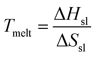 | (1) |
Ordering in 2D liquid phases has a long history. In the 1970's, Kosterlitz, Thouless, Halperin, Nelson and Young developed KTHNY theory which describes melting of 2D systems as the decoupling of pairs of topological defects and predicts an intermediate phase between solid and liquid called the “hexatic-phase”.38–42 In a solid 2D system, the crystal has long-range orientational order and quasi-long range translational ordering as a result of reduced dimensionality, the hexatic phase exhibits quasi-long range orientational order and short range translational order while in the liquid phase both translational and orientational order are short range.43,44 Although KTHNY theory and the existence of the hexatic-phase were originally developed for extended 2D systems, without consideration of free surfaces45 the hexatic phase has been positively identified in supercooled liquid metal surfaces.46
In this study, we extend the previous work by our group on the thermal stability of 2D Ga by using ab initio molecular dynamics (AIMD) simulations to determine the Tmelt of 2D Ga as the thickness is increased from four (quad-layer), to five (penta-layer) and six (hexa-layer) atomic layers. Furthermore, we explore the relevance of the hexatic phase in the thermal stability of these systems.
Methodology
All calculations use plane-wave density functional theory (DFT) within the Vienna ab initio Simulation Package (VASP)47 and the projector-augmented wave (PAW) method.48 For all calculations, a plane wave cut off of 350 eV was used. Methfessel–Paxton (order one) smearing with a width of 0.05 was used and all calculations were converged electronically to 1 × 10⁻⁶ eV. We use the Perdew–Burke–Ernzerhof for solids (PBEsol) exchange-correlation functional.49 For a variety of elements PBEsol has been shown to be effective at predicting melting temperatures in agreement with experiment.50 The thermal stability of bulk Ga has only been calculated using PW91 and was found to be 212 K;29 91 K below the experimental bulk Tmelt. Interestingly, it has been shown for Ga20+, Ga32+, Ga34+ and Ga35+ nanoclusters that adding +90 K to the calculated PW91 melting temperatures provides agreement with experimentally yielded results (it should be noted, however, that there are two exceptions).28 Further, tri-layer calculations undertaken by our group found that the using PW91 the tri-layer melts 91 K lower than using PBEsol.24 Assuming that the melting temperature difference between PW91 and experiment of 90 K is consistent between nanoclusters and 2D Ga, we conclude that PBEsol provides results that are comparable to within 1 K of experiment.Optimisations
The (010) termination of α-Ga was used to build structures that enabled the AIMD simulations to be seeded (see ESI† for more details). The initial α-Ga crystal was taken from the Crystallography Open Database with unit cell dimensions of 4.527 × 7.645 × 4.511 Å.11 Surfaces of four, five and six atomic layers were built containing eight, ten and twelve atoms per unit cell, respectively (Fig. 1a). Non-spin polarized optimisations of the structures were carried out using a Monkhorst–Pack k-point grid of 7 × 7 × 1 and k-point converged to within 0.1 kJ mol−1.Annealing
Supercells of each surface were created by repeating the optimised (010) α-Ga surfaces by 4 × 4 × 1, resulting in supercells of 128, 160 and 192 atoms for the quad-, penta- and hexa-layer systems, respectively. Single point Γ-centred k-points were used for all AIMD simulations. The annealing calculations were run in a nPT ensemble using the Parrinello–Rahman method51,52 with a Langevin thermostat. The nPT simulations were used only to equilibrate the structures at a range of finite temperatures and 0 kB pressure. The structures were annealed by incrementing the temperature by 80 K over 0.9 ps sequentially using a timestep of 3 fs until a melting transition was provisionally observed using root mean square displacement (RMSD) analysis. High temperature solids were then equilibrated for 9 ps before finite temperature melting simulations were seeded.Melting simulations
Finite temperature melting simulations were calculated within the nVT ensemble. Temperatures were selected to cover a minimum 100 K range at 20 K intervals with a timestep of 4 fs. For the quad-layer, temperatures ranged from 410–550 K, for the penta-layer, temperatures simulated were 300–420 K and for the hexa-layer, calculated temperatures ranged from 400–500 K. The AIMD simulations were run for a minimum of 100 ps per temperature. Specific heat curves were calculated using the multiple histogram method53 using the final 64 ps of each simulation to allow sufficient time for the structure to equilibrate and at 20 K increments to provide sufficient overlap of the finite temperature histograms.Results and discussion
2D polymorphism
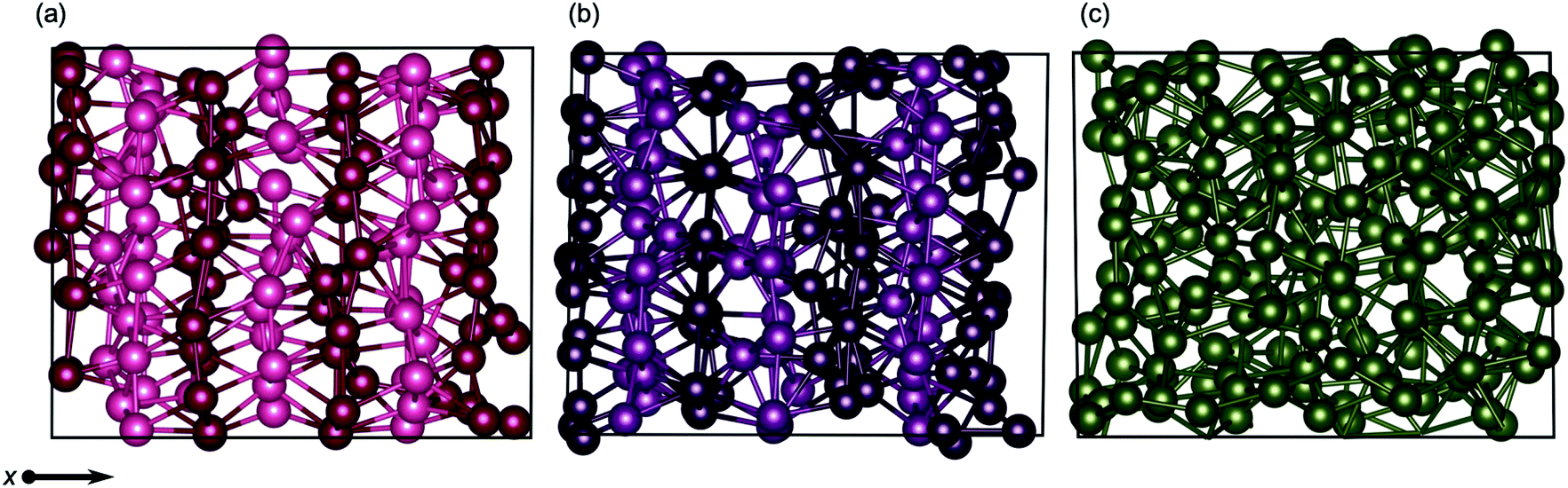
As the quad-, penta- and hexa-layer systems were annealed, all systems changed phase to a lower energy structure (Fig. S1†). The systems changed phase at different temperatures (82 K, 124 K and 67 K, for quad-layer, penta-layer and hexa-layer, respectively) and changed to structures distinct from each other (Fig. 1b–g).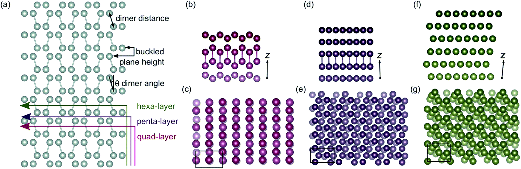 | ||
| Fig. 1 (a) Bulk α-Ga supercell with illustrations showing the cuts used to obtain the initial quad-layer (red line), penta-layer (purple line) and hexa-layer (green line) structures used to seed the MD simulations. The dimer distance, buckled plane height and dimer angle parameters are also defined. The optimised lowest energy Ga structures resulting from a phase change at temperature for (b) and (c), the quad-layer, (d) and (e), the penta-layer and (f) and (g), the hexa-layer. Perspectives along the x-axis, with the z-axis marked are shown in (b), (d) and (f) and perspectives along the z-axis are shown in (c), (e) and (g). The black boxes in (c), (e) and (g) show the unit cell. The cut off for the bonds was set to 2.7 Å. | ||
In order to quantify the structural change resulting from the phase-change, three parameters in bulk α-Ga are defined; dimer distance, dimer angle and buckled plane height (Fig. 1a). For bulk α-Ga, the dimer distance is 2.49 Å, dimer angle, relative to the z axis, is 17.3° and the buckled plane height is 1.44 Å (Table S2†). In the quad-layer structure, the dimers are maintained, although the dimer distance is extended to 2.68 Å while the dimer angle is significantly reduced to 1.0° (Fig. 1b and c). The buckled plane height varies from a maximum of 3.39 Å to a minimum of 1.86 Å (Table S2†) due to the corrugation in metallic surface layers and the offset of Ga2 dimers in the z direction. The radial distribution function (RDF) shows that the quad-layer is not geometrically similar to either the bulk α- or β-Ga (Fig. S2a†).
In the penta-layer structure, the phase change increases the dimer distance to 2.65 Å, reduces the dimer angle to 0.7° and increases the buckled plane height, which, in this case, is simply the plane height as the planes no longer buckled, to 2.41 Å (Fig. 1d and e, Table S2†). The RDF analysis does not show distinct similarity to either bulk α- or β-Ga (Fig. S2b†).
The optimisation of the hexa-layer phase-change structure results in the expansion of the system in the z dimension, such that no two Ga atoms are within 2.7 Å of one another. Thus, in the hexa-layer system, there are no Ga dimers analogous to those seen in bulk α-Ga (Fig. 1f and g) and the parameters used to define bulk α-Ga cannot be used to define the hexa-layer system. We note, however, that the interlayer distance stays reasonably constant between all of the layers at approximately 2.5 ± 0.1 Å. The RDF analysis shows that the hexa-layer system is not similar to bulk α- or β-Ga (Fig. S2c†).
We interpret the reduction in dimer angles and the extension of the interlayer distances from the bulk in all three of the systems to indicate that they are adopting a more traditional metallic-like close packed structure.
Electronic structure
Considering the electronic properties of the quad-layer system, the projected density of states (Fig. 2a), electron localisation function (ELF) analysis (Fig. S3b†), and band structure (Fig. S4a†) show that the lowest energy quad-layer structure is fully metallic as there is no band-gap present in the density of states which might indicate a different electronic behaviour of this system. Furthermore, there is no α-Ga-like pseudogap apparent in the density of states at the Fermi level.54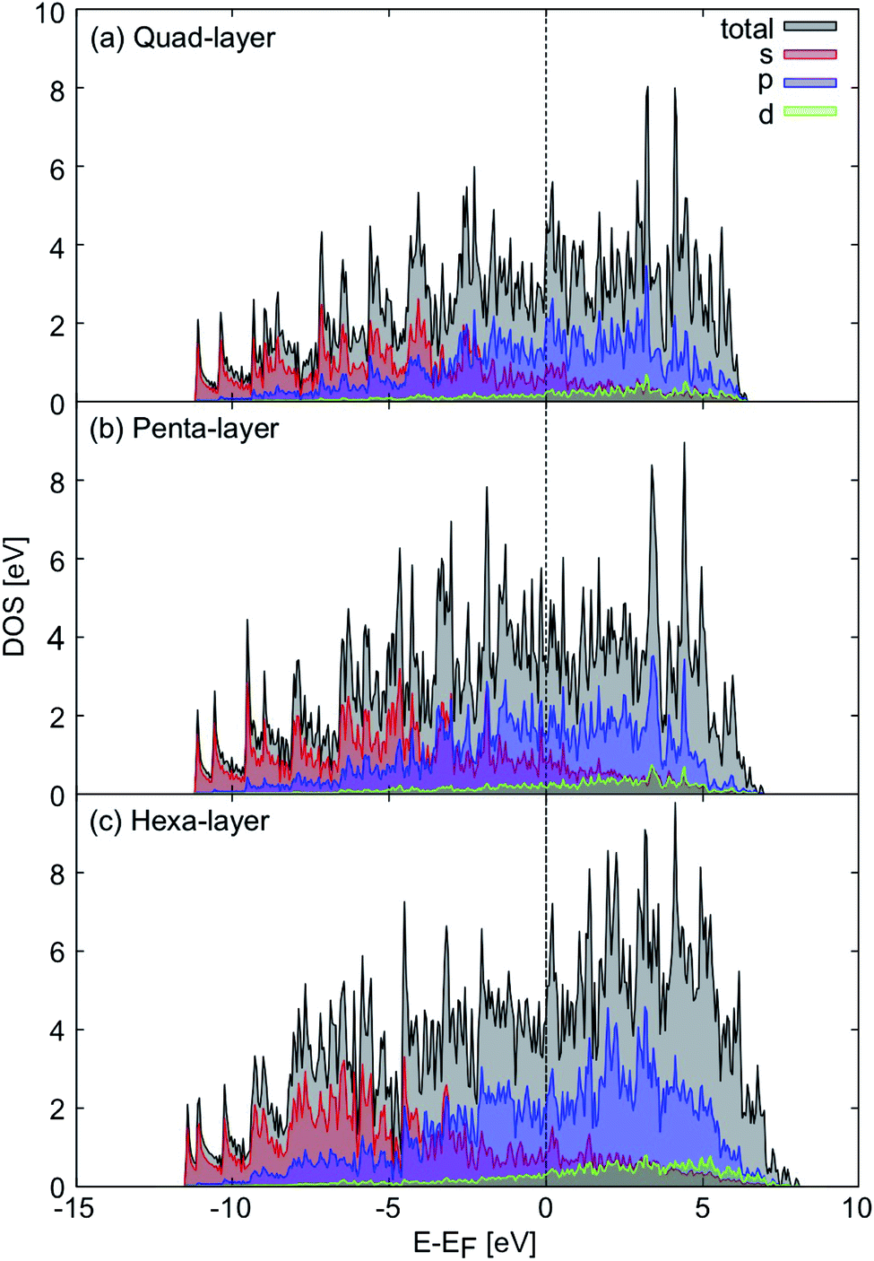 | ||
| Fig. 2 Projected density of states, relative to the Fermi level (black dotted line) for the (a) quad-layer, (b) penta-layer and (c) hexa-layer structures. Total density of states is shown in black, s orbitals are shown in red, p orbitals in blue and d orbitals in green. | ||
Evidence for fully metallic behaviour in the penta-layer structure is provided by the projected density of states (Fig. 2b). This analysis is reinforced by the ELF analysis which shows there is no covalent bonding in the penta-layer structure (Fig. S3c†) and by the band structure which shows metallic character (Fig. S4b†). As with the quad-layer system, the density of states shows no α-Ga-like pseudogap54 or band-gap, characteristic of an semi-conductor or insulator.
The density of states show that the hexa-layer system is also metallic (Fig. 2c) due to the lack of band-gap or pseudogap in the density of states, which is confirmed by the ELF analysis showing electron density localised on the atomic centres (Fig. S3d†) and the band structure (Fig. S4c†).
Based on the density of states, 2D Ga structures between two and six atomic layers are electronically indistinguishable (Fig. 2).24 Due to the fact that there is minimal variation in the electronic properties of 2D Ga systems up to six atomic layers thick, it could be advantageous to synthesise 2D Ga that is not ultra-thin. Using thicker forms of 2D Ga may enable the structure to be more robust for use in electronic applications.
The disappearance of covalency within 2D Ga structures, as evidenced by the ELF analyses (Fig. S3†) is not unprecedented. This phenomenon has also been observed in quasi-2D Ga nanoclusters (<100 atoms) where no α-like phase or covalent dimers are observed.19 Thus, the 2D Ga systems considered in this study have a closer structural similarity to quasi-2D nanoclusters than to bulk α-Ga. Interestingly, ELF analyses of optimised 2D slabs from a thickness of two to 12 atomic layers show that bulk-like structure and covalency reappears at a minimum thickness of 10 atomic layers (Table S3†).
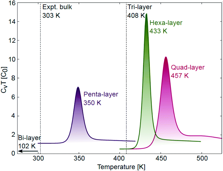 | ||
| Fig. 3 Specific heat curves for quad-layer (red), penta-layer (purple) and hexa-layer (green) 2D Ga with melting transitions observed at 457, 350 and 433 K, respectively. Tmelt for the bi-layer (102 K) and tri-layer (408 K) are taken from ref. 24. | ||
Thermal stability
The AIMD simulations find that the quad-layer system melts at 457 K, the penta-layer system at 350 K and the hexa-layer system at 433 K (Fig. 3). Therefore, 2D Ga from four to six atomic layers thick is thermally stable to well above the bulk Ga Tmelt. Furthermore, the variation in Tmelt of the quad-, penta- and hexa-layer 2D Ga systems is not monotonic, nor does it converge toward the bulk Tmelt with increasing thickness. Convergence towards the bulk Tmelt is expected around a thickness of 10 atomic layers (∼2 nm), as this is where the ELF analysis shows the return of covalently bound Ga2 dimers characteristic of bulk α-Ga (Fig. 4b and c, Table S3†). We highlight that the return of bulk-like bonding at a thickness of ∼2 nm corresponds to the return of approximately bulk Tmelt observed in Ga94 nanoclusters (∼2.4 nm in diameter), therefore loosely agreeing with our predictions here.55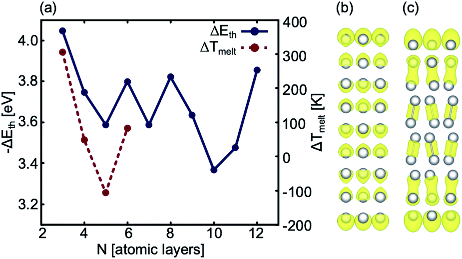 | ||
| Fig. 4 (a) Blue: The stability gained per atom as a result of adding a bulk atom to the system as the thickness of the slab is increased. Note that we use −ΔEth to show this correlation. Red: ΔTmelt between 2D Ga systems with N and (N − 1) layers, (b) ELF analysis of a 9 atom thick 2D Ga structure, and (c) ELF analysis of a 10 atom thick 2D Ga. | ||
Using ground state optimisations of 2D Ga systems, up to 12 atomic layers thick, we examine the stability gained from adding a bulk atom to the system as the thickness of the slab is increased, Eth, using the following relation:
 | (2) |
Structural analysis of melting
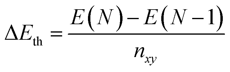
The average RDF in the solid phase, shows that the quad-layer and hexa-layer system are very similar, while the penta-layer solid system exhibits more peaks (Fig. 5a). The angular distribution function (ADF) analysis in the solid state for all systems show peaks occurring at the same angles, varying only in their intensity (Fig. 5c). RDF and ADF analyses of the liquid state show analogous behaviour of all three systems (Fig. 5b and d).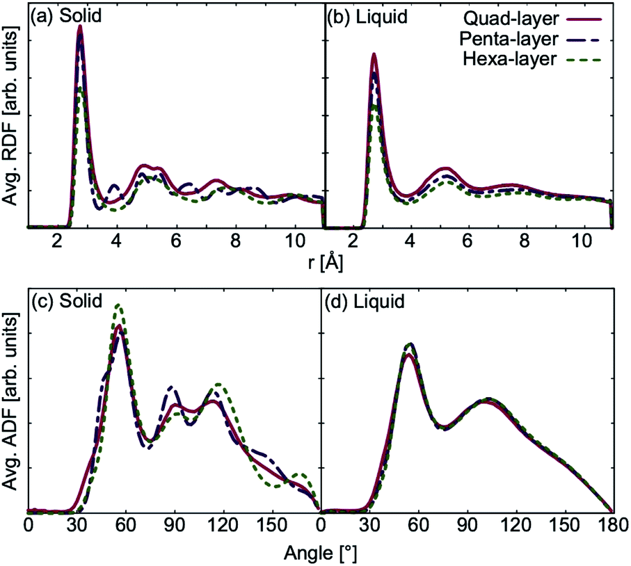 | ||
| Fig. 5 Average radial distribution function (RDF) for quad-layer, penta-layer and hexa-layer in the (a) solid phase and (b) liquid phase. Average angular distribution function (ADF) for quad-layer, penta-layer and hexa-layer in the (c) solid phase and (d) liquid phase. For the quad-layer (red), solid is defined as 410 K and liquid as 550 K; for penta-layer (purple), solid is 300 K and liquid is 420 K; for hexa-layer (green), solid is 400 K and liquid is 500 K. | ||
Using the change in RDF and ADF between the high-temperature solid and liquid state as a rough proxy for the degree of structural reorganisation upon melting, the penta-layer system exhibits a greater structural change, corresponding to a greater change in entropy. From the Tmelt relationship, eqn (1), it follows that a greater change in entropy upon melting leads to a lower melting temperature, agreeing with our results.
Average mean square displacement (MSD) analyses were used to examine the solid–liquid transitional structures. Transitional structures result from the finite temperature simulations closest to the calculated Tmelt for each system; 450 K simulation for the quad-layer system (Tmelt = 457 K), 340 K simulation for the penta-layer system (Tmelt = 350 K) and 440 K simulation for the hexa-layer system (Tmelt = 433 K). x- and y-dimensions are labelled as “in-plane” (repeated infinitely) while the z-dimension is finite and diffusion in this direction is termed “inter-planar.”
For the quad-layer system, the MSDy is highest while MSDx and MSDz are considerably lower (Fig. 6a). Thus, it follows that atomic diffusion in the y-dimension is higher than in the x- and z-dimensions.
 | ||
| Fig. 6 Average mean square displacement (MSD) for (a) quad-layer at an average temperature of 450 K, (b) penta-layer at an average temperature of 340 K and (c) hexa-layer at an average temperature of 440 K. MSDx is shown in blue, MSDy in red and MSDz in yellow. | ||
The penta-layer MSD analysis shows that MSDx is roughly equal to MSDy, and both are considerably higher than MSDz (Fig. 6b). Therefore, in-plane diffusion is roughly uniform, while inter-planar diffusion is limited.
The MSD analysis shows that, for the hexa-layer system, MSDy is only slightly higher than MSDx (Fig. 6c). MSDz is low, in keeping with the quad- and penta-layer systems (Fig. 6c). Similar to the penta-layer system, MSD analysis of the hexa-layer system shows that in-plane diffusion is higher than inter-planar diffusion.
Perpendicular surface ordering
In order to explain the non-uniformity of in-plane atomic diffusion of the quad-layer system resulting from the MSD analyses, so-called “single-coordinate atomic trajectories” were plotted for all three systems. The single coordinate atomic trajectories show the x, y, and z positional coordinates of all of the atoms in the system over simulated time to provide structural information about the movement of the atoms in each dimension (Fig. 7 and S5–S7†).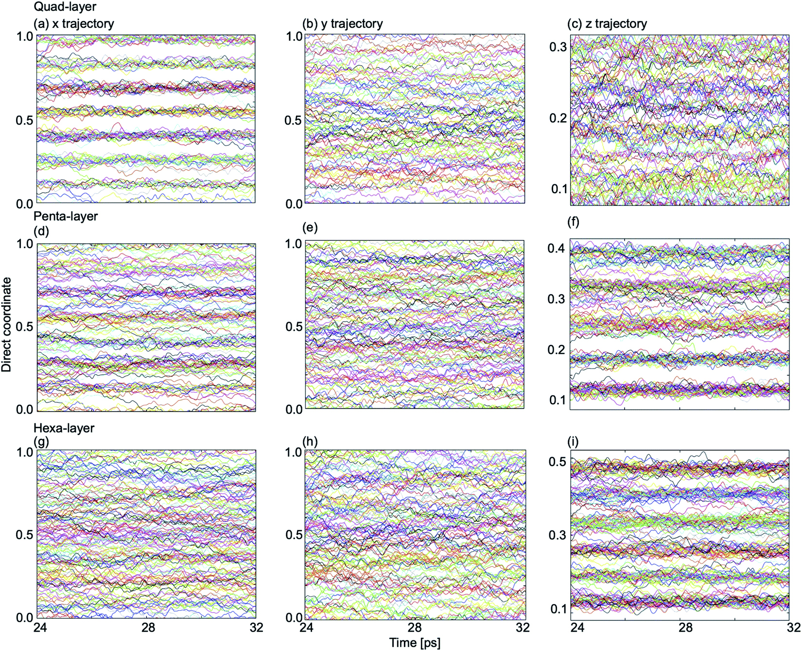 | ||
| Fig. 7 Single coordinate atomic trajectories in the x-dimension (left column), y-dimension (center column) and z-dimension (right column) for (a)–(c), the quad-layer system at 440 K; (d)–(f) the penta-layer system at 340 K; and (g)–(i) the hexa-layer system at 440 K. Note that the direct coordinates for the z-dimension are different due to vacuum requirements of modelling a 2D surface. | ||
In the quad-layer system, clear layering is seen in the x-dimension (Fig. 7a). We interpret this to mean that atomic diffusion in the x-dimension is limited, thereby explaining the low MSDx (Fig. 6a). We attribute the lack of definition in the z-dimension (Fig. 7c) to be the result of surface corrugation and offset Ga2 dimers, as seen in the phase-change structures (Fig. 1b and c).
For the penta-layer system, vague layering is seen in the x-dimension (Fig. 7d), however, no layering is seen in the y-dimension (Fig. 7e). Despite layering in the x-dimension, MSDx is roughly equal to MSDy (Fig. 6b). We expect that MSDx is high because while layers are seen in the x-dimension they are transient (Fig. S6a†). Inter-planar layers are very clear (Fig. 7f) and correspond well to the low MSDz (Fig. 6b).
Finally, for the hexa-layer system, no ordering is seen in the in-plane single coordinate atomic trajectories (Fig. 7g and h) which is reflected in approximately equal MSDx and MSDy (Fig. 6c). Interplanar layering is clear (Fig. 7i) and this is reflected in MSDz (Fig. 6c).
Observing layers in the z-dimension corresponds to layering parallel to the surface; a well-known phenomenon in liquid metal surfaces.36,56–59 Our results show that parallel surface layering at the Ga/vacuum interface is present in the quad-, penta- and hexa-layer transitional 2D Ga structures and therefore this ordering does not appear to be thickness dependent.
Layering in the x-dimension means that the quad-, and for a brief moment in time, penta-layer, systems are ordering perpendicular to the Ga/vacuum interface. This phenomenon has, to date, only been deduced experimentally.60,61 Furthermore, the current study is, to the authors' knowledge, the first report of perpendicular layering at a liquid metal/vacuum interface. The appearance of perpendicular ordering at the Ga/vacuum interface at a minimum thickness of four and a maximum of five atomic layers illustrates that this structuring is highly sensitive to slab thickness (Fig. 8). An experimental study proposed that perpendicular layering at a Ga/C(111) interface could be attributed to the alignment of Ga2 dimers imposed by the C(111) surface.60 While we do not have an opposing crystal to dictate the surface structure nor covalently bound Ga2 dimers, we expect that the formation of a Ga surface at the Ga/vacuum interface imposes ordering on the layers beneath.
 | ||
| Fig. 8 Snapshots of transitional structures for (a) quad-layer (450 K), (b) penta-layer (340 K) and (c) hexa-layer (440 K) structures. Atoms in successive x-layers are differentially shaded to guide the eye. No x-ordering is seen in the hexa-layer system. Black boxes show the unit cell. | ||
Finally, the ordering exhibited by these systems both parallel and perpendicular to the surface was examined in detail to ascertain if it is, in fact, the well known hexatic phase of 2D melting.38–42 We are, unfortunately, unable to conclusively diagnose the hexatic phase, due to the trade-off between simulating the “quasi-long range” effects required for a positive identification of the hexatic phase while still remaining computationally tractable. Despite this limitation, the orientational order correlation parameter, g6(r), was calculated up to 20 Å in the xy plane. There are limitations in defining an xy plane, particularly for the quad-layer structure where the planes are corrugated (Fig. 1b), therefore “in-plane” is defined as being within a z range of atom i to which the g6(r) parameter is measured. For the quad-layer system, hexatic-like ordering is observed through the melting transition (Fig. S8a†). In contrast to this, the solid and liquid penta-layer systems did not exhibit a high-degree of hexatic-like ordering, however, around the melting temperature (340 K) hexatic-like ordering appeared (Fig. S8b†). For the hexa-layer structure, hexatic-like ordering was observed in the solid but not through the melting transition nor in the liquid (Fig. S8c†). Importantly, we note that more definitive layering the x-dimension does not correspond to a higher degree of hexatic-like ordering. Therefore, x-ordering is not diagnostic of a hexatic-phase melting transition but rather is a structural feature of thin 2D Ga systems.
For all of these thin 2D Ga systems, parallel ordering inherent at finite thickness results in a reduction in entropy of the liquid. This reduction in mobility likely explains the raised Tmelt of these systems, in the same way that is observed for quasi-2D liquid Ga nanoclusters.29 Emergence of perpendicular ordering in the quad- and penta-layer systems seen here will also have entropic effects, however this ordering is more equally distributed across both the solid and liquid phases. Therefore, the entropic effects of perpendicular layering are not reflected in the ΔS upon melting, thus explaining why the quad- and penta-layer systems can exhibit such different melting temperatures. However, the emergence of this perpendicular ordering for these two systems of atomically-precise thickness—four and five layers—is evidence of how sensitive structure is to thickness, which we see reflected in highly variable melting temperatures.
Conclusions
The thermal stability of 2D Ga four, five and six atomic layers thick is considerably greater than the bulk thermal stability. Furthermore, the electronic structure of these systems is fully metallic for all, thus removing the necessity for the thickness of the 2D system to be atomically resolved when synthesising these materials for electronic applications. We propose that the change in thermal stability of the 2D structure can be estimated from the difference in stability due to thickness up to 10 atomic layers thick. For the first time, layering both parallel and perpendicular to a liquid metal/vacuum interface is reported. We determine that, despite ordering in the x-dimension, this is not indicative of a hexatic-phase melting transition. These results demonstrate both the dramatic variability of the stability of 2D Ga as a function of thickness and provide the prospect of synthetic techniques finding thicker forms of 2D Ga that are stable at higher temperatures.Conflicts of interest
There are no conflicts of interest to declare.Acknowledgements
The authors wish to acknowledge the use of New Zealand eScience Infrastructure (NeSI) high performance computing facilities. New Zealand's national facilities are provided by NeSI and funded jointly by NeSI's collaborator institutions and through the Ministry of Business, Innovation and Employment's Research Infrastructure programme. https://www.nesi.org.nz.References
- H. Morkoç and N. Mohammed, High-luminosity blue and blue-green gallium nitride light-emitting Diodes, Science, 1995, 267, 51–55 CrossRef.
- N. Zheludev, Single nanoparticle as photonic switch and optical memory element, J. Opt. A: Pure Appl. Opt., 2006, 8, S1–S8 CrossRef.
- S. Vivekchand, C. Engel, S. Lubin, M. Blaber, W. Zhou, J. Suh, G. Schatz and T. Odom, Liquid plasmonics: manipulating surface plasmon polaritons via phase transitions, Nano Lett., 2012, 12, 4324–4328 CrossRef CAS.
- A. Krasavin and N. Zheludev, Active plasmonics: controlling signals in Au/Ga waveguide using nanoscale structural transformations, Appl. Phys. Lett., 2004, 84, 1416–1418 CrossRef CAS.
- P. Wu, C. Khoury, T. Kim, T. Yang, M. Losurdo, G. Bianco, T. Vo-Dinh, A. Brown and H. Everitt, Demonstration of surface-enhanced Raman scattering by tunable, plasmonic gallium nanoparticles, J. Am. Chem. Soc., 2009, 131, 12032–12033 CrossRef CAS.
- A. Marín, T. García-Mendiola, C. Bernabeu, M. Hernändez, J. Piqueras, J. Pau, F. Pariente and E. Lorsenzo, Gallium plasmonic nanoparticles for label-free DNA and single nucleotide polymorphism sensing, Nanoscale, 2016, 8, 9842–9851 RSC.
- Y. Lu, Q. Hu, Y. Lin, D. Pacardo, C. Wang, W. Sun, F. Ligler, M. Dickey and Z. Gu, Transformable liquid-metal nanomedicine, Nat. Commun., 2015, 6, 10066 CrossRef CAS.
- R. Eggert, Minerals go critical, Nat. Chem., 2011, 3, 688–691 CrossRef CAS.
- A. Jayaraman, W. Klement, R. Newton and G. Kennedy, Fusion curves and polymorphic transitions of the group III elements – aluminium, gallium, indium and thallium – at high pressures, J. Phys. Chem. Solids, 1962, 24, 7–18 CrossRef.
- Y. Gutiérrez, M. Losurdo, P. García-Fernández, M. Sainz de la Maza, F. González, A. Brown, H. Everitt, J. Junquera and F. Moreno, Gallium polymorphs: phase-dependent plasmonics, Adv. Opt. Mater., 2019, 7, 1900307 CrossRef.
- A. Bradley, The cystal structure of gallium, Z. Kristallogr., 1935, 91, 302–316 CAS.
- V. Heine, Crystal structure of gallium, J. Phys. C: Solid State Phys., 1968, 2, 222–231 CrossRef.
- X. Gong, G. Chiarotti, M. Parrinello and E. Tosatti, α-Gallium: a metallic molecular crystal, Phys. Rev. B: Condens. Matter Mater. Phys., 1991, 43, 14278 CrossRef.
- N. Gaston and A. Parker, On the bonding of Ga2, structures of Gan clusters and the relation to the bulk structure of gallium, Chem. Phys. Lett., 2011, 501, 375–378 CrossRef CAS.
- N. Gaston and P. Schwerdtfeger, From the van der Waals dimer to the solid state of mercury with relativistic ab initio and density functional theory, Phys. Rev. B: Condens. Matter Mater. Phys., 2006, 74, 024105 CrossRef.
- N. Gaston, B. Paulus, K. Rosciszewski, P. Schwerdtfeger and H. Stoll, Lattice structure of mercury: influence of electronic correlation, Phys. Rev. B: Condens. Matter Mater. Phys., 2006, 9, 094102 CrossRef.
- K. Steenbergen, E. Pahl and P. Schwerdtfeger, Accurate, large-scale density functional melting of Hg: relativistic effects decrease the melting temperature by 160 K, J. Phys. Chem. Lett., 2017, 8, 1407–1412 CrossRef CAS.
- N. Drebov, F. Weigend and R. Ahlrichs, Structures and properties of neutral gallium clusters: a theoretical investigation, J. Chem. Phys., 2011, 135, 044314 CrossRef.
- K. Steenbergen and N. Gaston, First-principles melting of gallium clusters down to nine atoms: structural and electronic contributions to melting, Phys. Chem. Chem. Phys., 2013, 15, 15325–15332 RSC.
- V. Kochat, A. Samanta, Y. Zhang, S. Bhowmick, P. Manimunda, S. Asif, A. Stender, R. Vajtai, A. Singh, C. Tiwary and P. Ajayan, Atomically thin gallium layers from solid-melt exfoliation, Sci. Adv., 2018, 4, 1701373 CrossRef.
- K. Novoselov, A. Geim, S. Morozov, D. Jiang, Y. Zhang, S. Dubonos, I. Grigorieva and A. Firsov, Electric field effect in atomically thin carbon films, Science, 2004, 306, 666–669 CrossRef CAS.
- K. Novoselov, D. Jiang, F. Schedin, T. Booth, V. Khotkevich, S. Morozov and A. Geim, Two-dimensional atomic crystals, Proc. Natl. Acad. Sci. U. S. A., 2005, 102, 10451–10453 CrossRef CAS.
- D. Metin, L. Hammerschmidt and N. Gaston, How robust is the metallicity of two dimensional gallium?, Phys. Chem. Chem. Phys., 2018, 20, 27668–27674 RSC.
- K. Steenbergen and N. Gaston, Thickness dependent thermal stability of 2D gallenene, Chem. Commun., 2019, 55, 8872–8875 RSC.
- M. Ubaid, A. Aziz and B. Pujari, Adsorption of Na atom on mono-layer gallenene, AIP Conf. Proc., 2019, 2142, 110021 CrossRef CAS.
- M.-L. Tao, Y. B. Tu, K. Sun, Y.-L. Wang, Z.-B. Xie, L. Liu, M.-X. Shi and J.-Z. Wang, Gallenene epitaxially grown on Si(111), 2D Mater., 2018, 5, 035009 CrossRef.
- K. Steenbergen, D. Schebarchov and N. Gaston, Electronic effects on the melting of small gallium clusters, J. Chem. Phys., 2012, 137, 144307 CrossRef CAS.
- K. Steenbergen and N. Gaston, Geometrically induced melting variation in gallium clusters from first principles, Phys. Rev. B: Condens. Matter Mater. Phys., 2013, 88, 161402 CrossRef.
- K. Steenbergen and N. Gaston, A two-dimensional liquid structure explains the elevated melting temperatures of gallium nanoclusters, Nano Lett., 2015, 16, 21–26 CrossRef.
- K. Steenbergen and N. Gaston, Quantum size effects in the size-temperature phase diagram of gallium: structural characterization of shape-shifting clusters, Chem.–Eur. J., 2014, 21, 2862–2869 CrossRef.
- A. Carvajal Jara, M. Fontana Michelon, A. Antonello and M. de Koning, Theoretical evidence for a first order liquid–liquid phase transition in Ga, J. Chem. Phys., 2009, 130, 221101 CrossRef.
- S. Cajahuaringa, M. de Koning and A. Antonelli, Dynamics near a liquid–liquid phase transition in a non-tetrahedral liquid: the case of Ga, J. Chem. Phys., 2012, 136, 064513 CrossRef.
- R. Li, G. Sun and L. Xu, Anomalous properties in the liquid–liquid phase transition in gallium, J. Chem. Phys., 2016, 145, 054506 CrossRef.
- C. Tien, C. Charnaya, W. Wang, Y. Kumzerov and D. Michel, Possible liquid–liquid transition of gallium confined in opal, Phys. Rev. B: Condens. Matter Mater. Phys., 2006, 74, 024116 CrossRef.
- L. Peng, E. Chen, S. Liu, X. Liu and Y. Yu, In situ high-temperature nuclear magnetic resonance characterisation of structural evolution in pure gallium melt, Phys. Rev. B, 2019, 100, 104113 CrossRef CAS.
- M. Regan, E. Kawamoto, S. Lee, P. Pershan, M. Maskil, M. Deutsch, O. Magnussen, B. Ocko and L. Berman, Surface layering in liquid gallium: an X-ray reflectivity study, Phys. Rev. Lett., 1995, 75, 2498–2501 CrossRef CAS.
- J. Drewitt, F. Turci, B. Heinen, S. Macleod, F. Qin, A. Kleppe and O. Lord, Structural ordering in liquid gallium under extreme conditions, Phys. Rev. Lett., 2020, 124, 145501 CrossRef CAS.
- J. Kosterlitz and D. Thouless, Long range order and metastability in two dimensional solids and superfluids, J. Phys. C: Solid State Phys., 1972, 5, 124–126 CrossRef.
- J. Kosterlitz and D. Thouless, Ordering, metastability and phase transitions in two dimensional systems, J. Phys. C: Solid State Phys., 1973, 6, 1181–1203 CrossRef CAS.
- B. Halperin and D. Nelson, Theory of two-dimensional melting, Phys. Rev. Lett., 1978, 41, 121–124 CrossRef CAS.
- D. Nelson and B. Halperin, Dislocation-mediated melting in two dimensions, Phys. Rev. B: Condens. Matter Mater. Phys., 1979, 19, 2457–2484 CrossRef CAS.
- A. Young, Melting and the vector Coulomb gas in two dimensions, Phys. Rev. B: Condens. Matter Mater. Phys., 1979, 19, 1855–1866 CrossRef CAS.
- U. Gasser, C. Eisenmann, G. Maret and P. Keim, Melting of crystals in two dimensions, ChemPhysChem, 2010, 11, 963–970 CrossRef CAS.
- N. Negulyaev, V. Stepanyuk, L. Niebergall, P. Bruno, M. Pivetta, M. Ternes, F. Patthey and W. Schneider, Melting of two-dimensional adatom superlattices stabilized by long-range electronic interactions, Phys. Rev. Lett., 2009, 102, 246102 CrossRef CAS.
- B. Li, F. Wang, D. Zhou, Y. Peng, R. Ni and Y. Han, Modes of surface premelting in colloidal crystals composed of attractive particles, Nature, 2016, 531, 485–488 CrossRef CAS.
- F. Celestini, F. Ercolessi and E. Tosatti, Can liquid metal surfaces have hexatic order?, Phys. Rev. Lett., 1997, 78, 3153 CrossRef CAS.
- G. Kresse and J. Furthmüller, Efficient iterative schemes for ab initio total-energy calculations using a plane-wave basis set, Phys. Rev. B: Condens. Matter Mater. Phys., 1996, 54, 11169 CrossRef CAS.
- P. Blöchl, Projector augmented-wave method, Phys. Rev. B: Condens. Matter Mater. Phys., 1994, 50, 17953–17979 CrossRef.
- J. Perdew, A. Ruzsinszky, G. Csonka, O. Vydrov, G. Scuseria, L. Constantin, X. Zhou and K. Burke, Restoring the density-gradient expansion for exchange in solids and surfaces, Phys. Rev. Lett., 2008, 100, 136406 CrossRef.
- U. Pedersen, F. Hummel, G. Kresse, G. Kahl and C. Dellago, Computing Gibbs free energy differences by interface pinning, Phys. Rev. B: Condens. Matter Mater. Phys., 2013, 88, 094101 CrossRef.
- M. Parrinello and A. Rahman, Polymorphic transitions in single crystals: a new molecular dynamics method, J. Appl. Phys., 1981, 52, 7182–7190 CrossRef CAS.
- M. Parrinello and A. Rahman, Crystal structure and pair potentials: a molecular-dynamics study, Phys. Rev. Lett., 1980, 45, 1196–1199 CrossRef CAS.
- R. Poteau, F. Spiegelman and P. Labastie, Isomerisation and phase transitions in small sodium clusters, Z. Phys. D, 1994, 30, 57–68 CrossRef CAS.
- E. Voloshina, K. Rosciszewski and B. Paulus, First-principles study of the connection between structure and electronic properties of gallium, Phys. Rev. B: Condens. Matter Mater. Phys., 2009, 79, 045113 CrossRef.
- K. Pyfer, J. Kafader, A. Yalamanchali and M. Jarrold, Melting of size-selected gallium clusters with 60–183 atoms, J. Phys. Chem. A, 2014, 118, 4900–4906 CrossRef CAS.
- M. Regan, P. Pershan, O. Magnussen, B. Ocko, M. Deutsch and L. Berman, Capillary wave roughening of surface-induced layering in liquid gallium, Phys. Rev. B: Condens. Matter Mater. Phys., 1996, 54, 9730–9733 CrossRef CAS.
- O. Magnussen, B. Ocko, M. Regan, K. Penanen, P. Pershan and M. Deutsch, X-ray reflectivity measurements of surface layering in liquid mercury, Phys. Rev. Lett., 1995, 74, 4444–4447 CrossRef CAS.
- E. DiMasi, H. Tostmann, O. Shpyrko, M. Deutsch, P. Pershan and B. Ocko, Surface induced order in liquid metals and binary alloys, J. Phys.: Condens. Matter, 2000, 12, A209–A214 CrossRef CAS.
- H. Tostmann, E. DiMasi, P. Pershan, B. Ocko, O. Shpyrko and M. Deutsch, Surface structure of liquid metals and the effect of capillary waves: X-ray studies on liquid indium, Phys. Rev. B: Condens. Matter Mater. Phys., 1999, 59, 783–791 CrossRef CAS.
- W. Huisman, J. Peters, M. Zwanenburg, S. de Vries, T. Derry, D. Abernathy and J. van der Veen, Layering of a liquid metal in contact with a hard wall, Nature, 1997, 390, 379–381 CrossRef CAS.
- M. Reedijk, J. Arsic, F. de Theije, M. McBride, K. Peters and E. Vlieg, Structure of liquid Sn on Ge(111), Phys. Rev. B: Condens. Matter Mater. Phys., 2001, 64, 033403 CrossRef.
Footnote |
| † Electronic supplementary information (ESI) available. See DOI: 10.1039/d0na00737d |
| This journal is © The Royal Society of Chemistry 2021 |