
 Open Access Article
 This Open Access Article is licensed under a Creative Commons Attribution-Non Commercial 3.0 Unported Licence
Advances in the electron diffraction characterization of atomic clusters and nanoparticles
Arturo
Ponce
 a,
Jeffery A.
Aguilar
bc,
Jess
Tate
d and
Miguel José
Yacamán
*e
a,
Jeffery A.
Aguilar
bc,
Jess
Tate
d and
Miguel José
Yacamán
*e
aDepartment of Physics and Astronomy, The University of Texas at San Antonio, San Antonio, Texas 78249, USA
bIdaho National Laboratory, Nuclear Science and Technology Division, Idaho Falls, Idaho 83415, USA
cLockheed Martin Space, Advanced Technology Center, Palo Alto, California 94304, USA
dUniversity of Utah, Scientific Computing Imaging Institute, Department of Electrical and Computer Engineering, Salt Lake City, Utah, USA
eDepartment of Applied Physics and Materials Science, Center for Materials Interfaces in Research and Applications, Northern Arizona University, Flagstaff, AZ, USA. E-mail: Miguel.Yacaman@nau.edu
First published on 16th November 2020
Abstract
Nanoparticles and metallic clusters continue to make a remarkable impact on novel and emerging technologies. In recent years, there have been impressive advances in the controlled synthesis of clusters and their advanced characterization. One of the most common ways to determine the structures of nanoparticles and clusters is by means of X-ray diffraction methods. However, this requires the clusters to crystallize in a similar way to those used in protein studies, which is not possible in many cases. Novel methods based on electron diffraction have been used to efficiently study individual nanoparticles and clusters and these can overcome the obstacles commonly encountered during X-ray diffraction methods without the need for large crystals. These novel methodologies have improved with advances in electron microscopy instrumentation and electron detection. Here, we review advanced methodologies for characterizing metallic nanoparticles and clusters using a variety of electron diffraction procedures. These include selected area electron diffraction, nanobeam diffraction, coherent electron diffraction, precession electron diffraction, scanning transmission electron microcopy diffraction, and high throughput data analytics, which leverage deep learning to reduce the propensity for data errors and translate nanometer and atomic scale measurements into material data.
 Arturo Ponce | Arturo Ponce is an Associate Professor and Associate Chair in the Department of Physics and Astronomy at the University of Texas at San Antonio. He leads the Structure Physics and Electron Microscopy group at UTSA. He received his PhD in Materials Science from the University of Cadiz, Spain, and worked as a postdoctoral researcher at UNAM, Mexico, and CNRS, France. His research spans the theoretical and experimental aspects of the atomic structures, physical properties, and manipulation of materials on the nanoscale based on electron–matter interaction phenomena such as electron diffraction, electron holography, electron dose-controlled, and in situ microscopy. |
 Jeffery A. Aguilar | Jeffery A. Aguiar is a recognized expert in materials engineering, analytical instrumentation, and intelligence and materials research spanning global and nationwide collaborations, including in premier national research facilities at national laboratories, in universities, and in industry. He possesses expert knowledge of ultra-high temperature radiation hardened energy materials, characterization, and informatics-based approaches. Prior roles include being an invited academic faculty member at the University of Utah and technical deputy director of the Nuclear Materials Discovery and Qualification Initiative at Idaho National Laboratory. Now a senior scientist at Lockheed Martin's Advanced Technology Center with a diverse group of researchers and technical staff, he focuses on advances in ultra-high strength materials and novel concepts to enable future space missions. Aguiar is a professional author of more than 50 peer-reviewed publications and technical contributions, and a professional committee member of the Materials Research Society. In addition, he is a recipient of the Idaho National Laboratory's prestigious early career award recognized for his expertise in materials, with five patents, including an innovative approach to materials discovery using deep learning. |
 Jess Tate | Jess Tate received his PhD in Bioengineering from the University of Utah. His experience in computational modeling, image processing, and software engineering carried over into material science research focused on improving the real-time processing of microscopy data. He is currently a Research Associate at the Scientific Computing and Imaging Institute. |
 Miguel José Yacamán | Miguel José Yacamán received his Bachelor's and Master's degrees in Physics, and a Ph.D. in Materials Science from the Universidad Nacional Autónoma de Mexico (UNAM), and performed postdoctoral work at the University of Oxford and at NASA-AMES Research Center in California. He has received Honoris Causa Doctorates from the Universidad Autónoma de Nuevo León and from the Universidad Nacional de Córdoba. He is currently a Professor at the Applied Physics and Materials Science Department of Northern Arizona University. He has supervised about 125 students and more than 100 post-doctoral researchers. He is fellow of the MRS, AVS, APS, MSA, and AAAS. He has more than 500 publications, and a h-index factor of 73. He has been awarded the National Prize in Exact Sciences from the Mexican Academy of Sciences, National Prize of Sciences in México, the John Weatley Award of the American Physical Society, the Exact Sciences Prize from the State of México, the Melh Award and the Distinguished Lecture of the U.S. Metals and Materials Society, and a Guggenheim Fellowship, among others. |
Introduction
One of the most active fields in nanotechnology is related to the synthesis and characterization of metallic confined nanostructures, such as nanoparticles and clusters. The precise control of the size and shape of such nanostructures is challenging. Traditionally, when a nanoparticle has a relatively small number of atoms it is referred to as a cluster, these are more prone to grow in a controlled atomic way with a very precise number of atoms.1–5 In recent years there has been impressive advances in the controlled synthesis of clusters.6–10 This has resulted in a new field named atomically precise chemistry. Even though the boundary between clusters and nanoparticles is not precisely known, a cluster size ranges from 1 to 2 nm with perhaps no more than 500 atoms. Two examples of metallic clusters are shown in Fig. 1a and b obtained by aberration-corrected scanning transmission electron microscopy (Cs-STEM). As the number of atoms increases the properties change. To understand the properties, it is necessary to know the structure of the cluster. The most extended method used is X-ray diffraction. Starting from the determination of the Au102 cluster11 several other clusters have been determined, such as Au25(SR)18, Au38(SR)24 (SR = cyclohexylthiol), Au30(S-tBu) and many others.12–14 The main difficulty in X-ray diffraction is the need for the single crystal to be reliable. That means that a supercrystal of clusters must be generated. This is not possible for all clusters and this is the main limitation of the technique. Additionally, X-ray diffraction is a technique in which averages over a large area and local cluster variations cannot be observed. Electron diffraction, on the other hand, is a local technique that can be used to determine the structure of individual clusters and nanoparticles. In this review we will discuss the methods of electron diffraction and will show that it has the same effectivity as X-ray diffraction and could become the most utilized technique for studying clusters and nanoparticles. | ||
| Fig. 1 Examples of gold cluster structures: (a) decahedron and (b) icosahedron. | ||
X-ray diffraction is produced by single scattering events (kinematical scattering). Electrons on the other hand interact with matter 104 times more than X-ray diffraction. Therefore, electron diffraction patterns contain a lot more information. However, a complication arises from the multiple scattering events that are present in electron diffraction, leading to dynamical effects. In the electron–matter interactions, shown in Fig. 2, k and k′, the incident and diffracted wavevectors satisfy the Laue condition. The difference vector k − k' = G, is the change owing to diffraction and represents an arbitrary point in the reciprocal space. The scattered beam satisfies the Bragg condition as |k| = |k'| = 2π/λ, with λ representing the wavelength. The multiple diffractions shown in Fig. 2 can fall into the allowed and forbidden ghkl positions, which are not allowed using the extinction rules calculated from the structure factor and makes elucidation of the crystal difficult, even for very thin crystals.15 The result is that the intensity of the spots is not equal to Fh2, in which Fh is the structure factor.15,16 In the case of a large diffraction this can be overcome using precession diffraction,17 as we will discuss in the following sections. However, for the case of a metallic cluster, with only a limited number of atoms, the situation is more complicated because the atomic arrays are not necessarily located in conventional crystallographic directions.
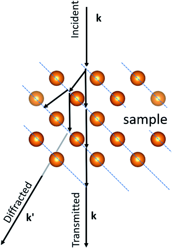 | ||
| Fig. 2 Multiple scattering events during electron diffraction. | ||
Fig. 3 shows the atomic planes on the cluster Au146 as reported by Vergara et al.18,19Fig. 3a is oriented along the [111] direction and Fig. 3b is oriented along the [1![[1 with combining macron]](https://www.rsc.org/images/entities/char_0031_0304.gif) 0] direction (both shown as fcc directions). As can be seen, the atoms are not aligned in well-defined columns projected along both directions (some of them are indicated by the arrows). In this way, electrons traveling through a cluster will suffer multiple scatterings and will register these small atomic variations. The resulting diffraction pattern is directly related to the cluster structure. This can also be rephrased, meaning that the Bragg law cannot be used in the case of clusters. The Bragg law requires scattering in at least 10 atomic rows in order to produce coherent interference of the electron waves.
0] direction (both shown as fcc directions). As can be seen, the atoms are not aligned in well-defined columns projected along both directions (some of them are indicated by the arrows). In this way, electrons traveling through a cluster will suffer multiple scatterings and will register these small atomic variations. The resulting diffraction pattern is directly related to the cluster structure. This can also be rephrased, meaning that the Bragg law cannot be used in the case of clusters. The Bragg law requires scattering in at least 10 atomic rows in order to produce coherent interference of the electron waves.
 | ||
| Fig. 3 Atomic order in two low index directions (in fcc notation) for the cluster Au144 (a) along the [111] direction and (b) view along the [110] direction view along the atomic distribution “seen” by the electron beam is not one of atomic columns oriented in an ordered manner. This will result in a complicated electron diffraction pattern.19 | ||
As the number of atoms increases the diffraction pattern will become more defined. In the case of nanoparticles that are greater than 5 nm in size, the diffraction pattern already shows features as size streaks which are well known for bulk crystals. Despite the difficulties it is possible to calculate the diffraction pattern of clusters considering a structural model and using a modified version of the multislice method,20 which does not require atomic potential periodicity. An important aspect to be emphasized is that X-ray diffraction implies an average of all the present structures; therefore, individual variations are lost. Even with the best separation methods available it cannot be assumed that all the clusters are identical. On the other hand, electron diffraction is a localized technique and if the spot size is controlled it is possible to obtain individual cluster patterns and test for structural variations. If the clusters are placed on a carbon grid for transmission electron microscopy (TEM) examination, 108 nanoparticles per cm2 are typically and estimated to be present. It is possible to obtain a huge amount of data, which allows researchers to employ machine learning methods for structural determination by using a database of the crystallographic information.
Radiation damage
Clusters and nanoparticles are very sensitive to radiation damage caused by the electron beam. To successfully study clusters and nanoparticles radiation damage must be controlled. The main mechanisms of radiation damage in protected metallic clusters are: (i) radiolysis, (ii) knock on effect of surface atoms, and (iii) the Auger effect.21 Radiolysis affects lighter atoms, for example ligands used to stabilize clusters, and the accelerating voltage is not the primary radiation damage. When the number of atoms is large, such as in 50 nm particles, the knock on effect of bulk atoms becomes important and the reduction of the accelerating voltage prevents the damage. Therefore, in each case we must find a compromise acceleration voltage to minimize the overall damage. Radiolysis can be recognized because carbon molecules from the ligand redeposit on the cluster and form a halo that blurs the image.The number of atoms in the nth shell of an icosahedron can be obtained by 10n2 + 2, here n is the cluster number. A common metal cluster is the 13-atom icosahedron (n = 1). The structure has one central atom and 12 surrounding atoms, 20 faces, 12 vertices and 30 edges. For subsequent numbers, the number of atoms adopts the form ni = ni−1 + (ni2 + 2); for example, n4 = 147 + (42 + 2) = 309. The sequence shown in Fig. 4 illustrates the cluster number and the estimated diameter, for cluster n = 21 one will obtain 33![[thin space (1/6-em)]](https://www.rsc.org/images/entities/char_2009.gif) 153 atoms and a nanoparticle of 11.504 nm, the structures were modeled in VESTA software.22 The transition from a cluster to a nanoparticle occurs when a plasmonic effect starts to appear. Clusters exhibit quantized properties as the quantum effects are dominant, this defines the unique properties of the specific cluster number. Clusters are unstable without the protection of their surfaces, which is given by ligands attached to their surfaces. For instance, the Au144(thiolate)60 cluster is stabilized by a thiolate group, 2 phenylethanethiolate.23
153 atoms and a nanoparticle of 11.504 nm, the structures were modeled in VESTA software.22 The transition from a cluster to a nanoparticle occurs when a plasmonic effect starts to appear. Clusters exhibit quantized properties as the quantum effects are dominant, this defines the unique properties of the specific cluster number. Clusters are unstable without the protection of their surfaces, which is given by ligands attached to their surfaces. For instance, the Au144(thiolate)60 cluster is stabilized by a thiolate group, 2 phenylethanethiolate.23
 | ||
| Fig. 4 Atomic models of the icosahedral metal cluster and nanoparticles for different values of n (1, 2, 3, 4, 6, 14, 19, and 21) and the total number of atoms upon growing the cluster to the nth shell. | ||
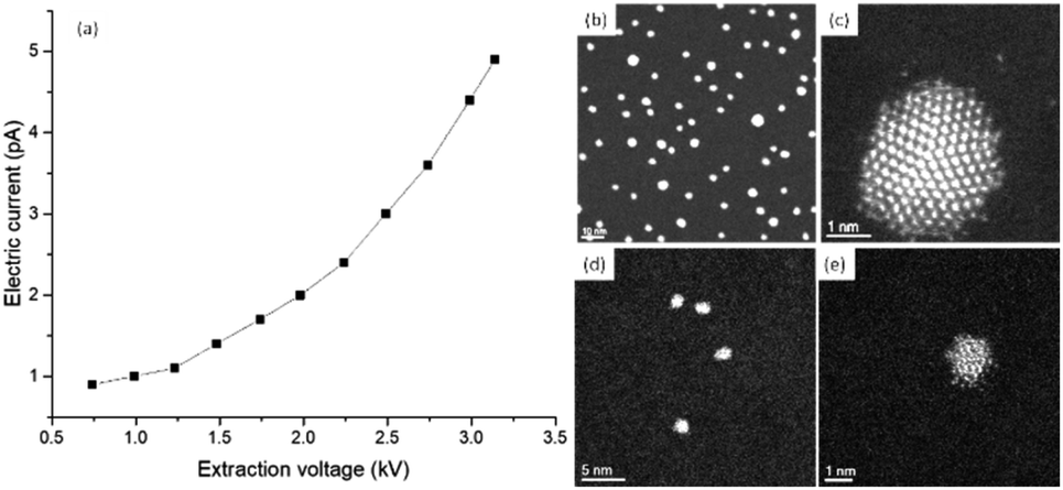
Beam sensitive samples, such as organic materials or ligand protected metallic clusters, require a much lower dose of electron beam radiation to avoid damaging the sample.24 There have been many developments that have improved the high resolution of microscopes at low dose configurations. One of these is the introduction of highly sensitive sensors, which allows the detection of single electron events.25,26 Low dose beam radiation can also be used in addition to other techniques that allow a wide range of new information that can be attained from the specimen. Electron diffraction methods at low dose configurations are another alternative to obtain the crystallography of biological and sensitive samples. Another methodology is phase retrieval in electron holography at low doses as a systematic approach to reduce the electron beam current in the sample.27–29 Detection is a very important aspect in low dose radiation and illumination cannot be visualized with binoculars using low doses. According to Buban, et al.,30 catalysts are believed to cause damage at the order of 100 e− Å−2, biological samples with sugar embedded specimens require doses of <20 e− Å−2, and biological samples kept under liquid nitrogen require doses of <5 e− Å−2. Many of these advances enabled progress in the methods used for increasing the high-resolution imaging methods using low dose configurations. For STEM, using a probe-corrected microscope, the diameter of the electron beam (∼1.0 Å) can resolve individual columns, but the current density increases substantially and deteriorates sensitive materials, such as the protected ligands of the clusters. To measure the number of electrons interacting with the specimen, one needs to use a Faraday cup to collect the electric current produced by the electron beam, which is an accurate device used to measure the electric current in the specimen region. Fig. 5a shows the experimental set up of the Faraday cup attached to a JEOL 2010F microscope and Fig. 5b shows an image of the electron beam collected at a magnification of 800 K using a complementary metal oxide semiconductor (CMOS) camera (TVIPS). When the Faraday cup is employed the number of electrons per area can be directly estimated. However, if the current density is measured on the screen the magnification must be considered, for example pA cm−2 (1 A = 1 C s−1 = 6.24 × 10¹⁸ electrons per s). Fig. 5b was collected using the minimum illumination possible by forcing the condenser lens voltage up to 8.06 V, the diameter of the region of illumination is shown in the intensity profile shown in Fig. 5c.
 | ||
| Fig. 5 (a) Experimental set-up of the Faraday cup device used to measure the electric current of the electron beam. (b) An electron beam probe registered at a magnification of 800 K, and (c) the intensity profile of an electron beam probe with a diameter of approximately 55 nm. | ||
In the microscope used, the current registered using the ammeter was 35 pA (diameter of the beam ∼ 55 nm), which corresponds to 920 electrons per Å2 per second. When the number of electrons is measured using the screen plate of the microscope (2.2 pA cm−2 at a magnification of 800 K times, 880 electrons per Å2 are registered), the number of electrons is about 40 electrons per Å2 less than the value obtained using the Faraday cup. The conversion used for the calculation is:31
| 2.2 pA cm−2 × 6241500 e− pA−1 × 1 s per frame × 1 × 10⁻¹⁶ cm2 Å−2 × 8000002 = 878 e− Å−2 s−1 |
If the same current density is shown on the screen, but the diameter is reduced to 2.5 nm, the number of electrons is about two orders of magnitude higher (∼4.4 × 10⁵ electrons per Å2 per s). The current density can also be modified using different apertures of the condenser lens.
Using STEM, the current density increases exponentially. Current densities measured using a JEOL ARM200F with a probe corrector are shown in Fig. 6a. The electric current values were obtained using the same Faraday cup as previously described. The aperture of the condenser lens used was set to 20 μm and the extraction voltage A2 was held constant. The curve shown in Fig. 6a was obtained by reducing the extraction voltage A1. The images shown in Fig. 6a–e were recorded using a high angle annular dark field detector (HAADF) in the STEM mode using standard emission in the microscope (A1 = 3.14 kV, A2 = 7.05 kV and a current measured of 4.9 pA). The HAADF-STEM images correspond to gold clusters of approximately 3.8 nm (Fig. 6b) and approximately 1.6 nm (Fig. 6d), both ligand-protected. When the field of view is reduced to approximately 9 × 9 nm, the bigger cluster is more stable to the electron dose (Fig. 6c), while the smaller cluster deteriorates (Fig. 6e). Using the currents measured for standard emission and a probe size of around 1 Å, the electron dose is approximately 4 × 10⁷ electrons per Å2. The electron dose measured from the curve in Fig. 6a is approximately 7 × 10⁶ electrons per Å2. In the measurements performed using the TEM mode, we considered the electron dose frame per second (fps) or fractions of seconds (usually 0.5 fps), which is relatively low speed compared with ultra-fast acquisition.32 In the STEM mode, the parameter that is used to control the electron dose is the dwell time, which is the time in which the electron beam is retained per pixel. In the STEM mode, there is a compromise between the dwell time and electron dose used to study a few atoms in a cluster with atomic resolution. When the knock on is significant the surface of the nanoparticle looks irregular and some atoms are dispersed outside the clusters, as shown in Fig. 6e. The damage produced by the emission of the Auger electrons can be significant. The Auger effect is produced by the filling of inner atomic shell vacancies by an electron in higher energy levels. The excess of energy is transfer to an outer shell electron, which is then emitted out of the atoms. The energy of the Auger electron can be released on the cluster or nanoparticle in the form of heat, this effect was analyzed by Williams33 to explain the shape fluctuations on the nanoparticles. Let us consider an Auger ionization event in a gold cluster. Every event produces 2 keV with a range of approximately 1.5 nm, which deposits approximately 0.3–0.4 eV per atom. For instance, if the electron dose is 104 electrons per Å2 per second in the Au144 cluster, 72 Auger events per second are generated. This will deliver 22.5 eV in the cluster every second. The clusters are placed on a carbon grid for observation in the TEM. As the ligand is an insulator there will be an increase in temperature on the cluster inducing radiation damage. For bigger nanoparticles, without the presence of ligands, part of the heat will be released to the substrate and the effect will be negligible.
 | ||
| Fig. 6 (a) Electron current versus extraction voltage in a JEOL ARM200F operated at 200 kV. HAADF-STEM images of gold thiolate protected clusters of approximately 3.8 nm at (b) medium magnification and (c) high resolution. Images of approximately 1.6 nm clusters at (d) medium magnification, and (e) an example of radiation damage in gold clusters; the particle shows erosion on the surface due to knock-on radiation. | ||
Diffraction methods in STEM mode
Selected area electron diffraction (SAED) is the most common method used to study the structure of materials. The reflections used for the analysis of SAED patterns that are inside the zero order Laue zone (ZOLZ) are not sufficient to extract the 3D structural information of a crystal and therefore several zone axes must be registered. However, under certain modes of optical configurations in the microscope (a large convergence angle and large camera length), it is possible to obtain information on reflections at the first-order, second-order, third order, and so on, which are known collectively as the higher-order Laue zones (HOLZ). The information in the HOLZ regions is commonly used for studying symmetry in crystallography.34,35 For clusters and nanoparticles, an electron beam confined as a nanoprobe can also be used to obtain diffraction patterns from individual nanoparticles and it can be combined with a scanning process in the STEM mode. In this process, the scanning is stopped to register the diffraction pattern of the selected nanoparticle. The switching process between STEM and diffraction is defined as the D-STEM method. When the electron probe is stopped in a cluster, the diffraction pattern can be recorded using the charge-coupled device (CCD) camera. Under this configuration, the lateral resolution in real space is reduced; however, the image of the cluster is still clear enough to identify the cluster or nanoparticle. Using aberration-corrected microscopes with the probe corrector, it is possible to reduce the convergence angle and separate the convergent disks to reflections when the beam is aligned in a quasi-parallel illumination. Electron diffraction patterns on the STEM patterns are obtained by positioning the beam in the STEM image using the Digiscan control, the scan is stopped in a region of interest and subsequently the pattern is recorded using a CCD camera. Fig. 7 shows diffraction patterns in the STEM mode under two different semi-convergence angles. | ||
| Fig. 7 Experimental and simulated examples of diffraction patterns using STEM mode. (a) An atomic model of a pentagonal nanoparticle, (b) a HAADF-STEM image of a pentagonal particle, indicating the position of the beam to extract the diffraction patterns with (c) a large convergence angle and (d) after the modification of the values of the corrector lens (quasi-parallel illumination). The simulation of the electron diffraction patterns under nanobeam diffraction are shown below: (e) the simulation of the diffraction pattern using a semi-convergence angle of 3 mrad and (f) the diffraction pattern simulated with an angle of 0.5 mrad. Atomic models of the simulated patterns indicate the simulated probe size interacting with the nanoparticle. | ||
The semi-convergence angle is directly associated with the probe size, at large convergence angles the convergent beam electron diffraction (CBED) disks are formed. The D-STEM mode generates CBED patterns, which are adjusted to obtain diffraction patterns with spots instead of modifying the condenser lens excitation value and the excitation voltage of the adaptor lenses (ADL) of the hexapole of a corrected electron optical system (CEOS) corrector. In this process, the beam is aligned by the beam tilt and beam shift deflectors. Fig. 7a shows the model of the pentagonal nanoparticle used in Fig. 7b, collected using a large convergence angle (Fig. 7c) and after the separation and reduction of the disks, the reflections are obtained (see Fig. 7d). The decahedron was used for practical purposes to illustrate the change from the large to the low convergence angle without deterioration of the sample. The consequence of the compensation can be simulated in a pentagonal particle (Fig. 7a) oriented near the zone axis of the experimental particle. The conditions for the simulations are a semi-convergence angle of 3 mrad (Fig. 7e), which is reduced to 0.5 mrad for quasi-parallel illumination, as shown in Fig. 7f. Simulations were performed using the java electron microscopy software package.36 Under these illumination conditions, the electron beam is not precisely a convergent beam, but a quasi-parallel illumination, in which the electron path is forced to a localized area in the nanometric scale with a parallel illumination at the same time.
For protected metallic clusters the electron beam irradiation is more critical owing to the high sensitivity of the ligands. To avoid damage, faster dwell times are employed before collection of the diffraction patterns. Fig. 8 shows a set of images to elucidate the structure of the cluster Au144SR(60). Fig. 8a shows a probe-corrected HAADF-STEM image and Fig. 8b shows the fast Fourier transform (FFT). Fig. 8c shows a simulated image of the metallic cluster (using simulaTEM37) and its diffraction pattern (Fig. 8d). Fig. 8e shows the HAADF-STEM image after adjustments for D-STEM, as shown in Fig. 8f. The position of the beam from which the diffraction pattern is obtained is indicated in Fig. 8e. The diffraction pattern was collected under quasi-parallel illumination. The analysis of the diffraction patterns and atomic resolution images provides structural characterization of the individual metallic clusters. A novel perspective on the diffraction methods used under the STEM mode has been recently demonstrated using cryo-electron ptychography,28 which has been employed for sensitive materials for low-dose phase retrieval. Ptychography is an interesting method, in which electron microscopy is explored either in the real space or reciprocal space. In real space, ptychography is analogous to off-axis electron holography, one of the complementary methods used for phase retrieval and applied to sensitive specimens.27,29,38
 | ||
| Fig. 8 An Au144SR(60) cluster recorded using (a) a HAADF-STEM image23 (FFT image shown in (b)) and (c) a simulated image (with the simulated diffraction pattern shown in (d)), and (e) the HAADF-STEM image adjusted via (f) D-STEM. | ||
Unlike the two alternative diffraction methods, electron and neutron diffraction, the analyses of electron diffraction are carried out in isolated clusters or nanoparticles, which makes the challenge more important given the high intensity of the electrons and the dynamic scattering, as previously explained. Similar to the two alternate techniques, data collection must be acquired in a few seconds or a fraction of a second. Even when the development of electron detectors is one step behind with respect to X-rays it is clear to see the complexity of identifying a single cluster owing to the multiple variables and the problem becomes analogous to the many body problem, not because we need to detect individual electrons that have deviated from the specimen, but the information from the wavefunction to the exit of the sample and the use of probabilistic methods is prevalent.
Crystal orientation mapping assisted with precession electron diffraction
Precession electron diffraction (PED) has been used to reduce dynamical scattering, as proved and theoretically supported by Paul Midgley and Roger Vincent.16,17,39,40 The conical oscillation of the electron beam (performed between 50 and 100 Hz) is produced by scanning the deflection of the scanning coils in the microscope. The method has been used to quantify the intensities for crystalline structure determination and also to enhance the electron energy loss spectroscopy (EELS)41 signal by compensating for channeling-induction.42,43 The reflections excited during the precession process satisfy the Bragg condition at each moment, making the dynamical effects less pronounced in the diffraction pattern. The intensities obtained are proportional to the square of the structure factor and the forbidden reflections are significantly reduced. Increasing the precession angle will make the Ewald sphere touch more points in the reciprocal space and more diffraction spots will be displayed in the diffraction pattern. Fig. 9a shows a STEM image of a polycrystalline YAG:Er sample, which was prepared using a focused ion beam (FIB), the inset shows the crystalline model generated using VESTA.22Fig. 9b and c shows the experimental results; the electron diffraction patterns with precession off and on oriented along the 〈113〉 zone axis, respectively. The evidence of the enhancement of the reflections is clear when the precession is activated. Fig. 9d shows the simulated electron diffraction pattern at a low camera length to show the zero and first order Laue zones (FOLZ) as seen in the experimental pattern shown in Fig. 9b. The diffraction pattern simulated and shown in Fig. 9e was obtained without precession and for a 50 nm electron-transparent thickness. Fig. 9f shows the simulated PED pattern with 1° of the precession angle, the experimental precession pattern corresponds to the quasi-kinematical case of the simulated pattern. Simulations were performed using the JEMS software package.34,36 The diffraction pattern of Fig. 9d was obtained with the double-diffraction activation in the JEMS program, which plots the kinematically forbidden reflections. | ||
| Fig. 9 (a) An STEM image of a YAG:Er polycrystalline sample; (b) a low camera length SAED pattern of an individual grain oriented along the 〈113〉 zone axis. (c) An experimental PED pattern collected at 1° in the same zone axis. (d) A simulated electron diffraction pattern at low camera length with double diffraction; (e) a simulated electron diffraction pattern without precession and with 50 nm of electron-transparent thickness; and (f) a simulated PED pattern at 1° for comparison with the experimental case. | ||
A systematic indexing and crystal orientation mapping applied to TEM has been developed41,44 and combined with precession electron diffraction. This technique has become a useful tool to obtain crystal orientations and phase maps in relative short times.45 The principle consists of forming a small probe to be scanned through the area of interest on the sample, obtaining and recording an electron diffraction pattern at each step of the scanned area with an ultrafast (200 fps) external CCD camera. Every acquired electron diffraction pattern is stored in a computer to be later compared to pre-calculated templates; the diffraction pattern is indexed using cross-correlation to select the best match. The indexing result of the whole set of diffraction patterns can then be displayed as a phase or an orientation map of the scanned area.46 When using precession, the effective focused beam size on the specimen will suffer from beam broadening owing to spherical aberration for the non-axial trajectories, and this will be more noticeable when increasing the precession angle. At the end, the spatial resolution of the orientation/phase map will depend on the effective beam size and on the scanning step chosen. On the other hand, the angular resolution obtained in the orientation maps will depend on the angular grid used for the generation of the templates. As the spot diffraction patterns are not sensitive to crystal tilts of less than 1°, values are usually given between 0.5° and 1°. Though there is the possibility of selecting a smaller sample value by increasing the number of generated templates so that between a given template and the closest one there is 0.2–0.5°.44 To avoid duplicities in the orientation assignation it is necessary to use precession angles lower than 1°. This must be taken into consideration when choosing the precession angle for phase or orientation mapping. Hence, the crystal orientation and phase mapping consist of two main steps: the fast acquisitions of spot patterns and the reliable orientation identification. This brings the necessity of additional hardware equipment that must be used with the microscope and software to carry out the analysis. The degree of matching between an experimental diffraction pattern and a calculated one is given by the following equation:44

In which, the pattern is represented by the intensity function P(x,y) while every template i is given by the function Ti(x,y). The highest Q value corresponds to the solution. In this way, the quality of the pattern matching can be evaluated by the assigned pixel values of the index maps. Additionally, a reliability index value is determined between the two highest optimum solutions Q1 and Q2 of the matching: R = 100(1 − Q2/Q1). A reliability index value will be low when more than one orientation or phase is contained in a diffraction spot pattern. This value is assigned to each pixel corresponding to an indexed diffraction pattern, in this way a reliability map can be generated. A lower value will correspond to a darker pixel and a higher value will correspond to a brighter pixel. The range will depend on the maximum reliability value calculated. To reconstruct a bright field image of the object, the average intensity is calculated in a disc that surrounds the transmitted beam from the recorded diffraction pattern (Fig. 10). The inner part of the transmitted beam saturates, leaving the contrast information in the outer part. Therefore, the virtual aperture needs to be larger than the transmitted beam. In this virtual bright field STEM mode, it is the beam diameter that delimits the virtual bright field image resolution.46 In a similar way, the virtual aperture may be displaced on one of the spots of the diffraction pattern and form a virtual dark field image.
 | ||
| Fig. 10 A schematic representation of the virtual bright field reconstruction. A virtual aperture is used to select only the transmitted beam and this is then plotted on the image. This is equivalent to introducing an aperture in the beam path (adapted with permission from ref. 47). | ||
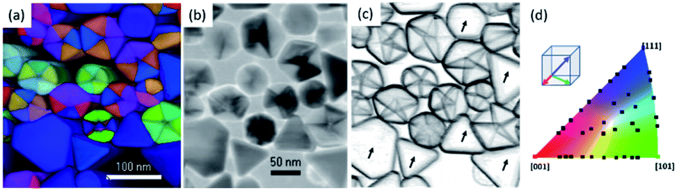
An example of the crystal orientation mapping is shown in Fig. 11 in which the gold pentagonal nanoparticle is orientated along the observation axis z (zone axis). The orientation map with respect to z is colored in green, showing an orientation of [110] for the whole nanoparticle. The index map shows dark areas along the twin boundaries of the particle owing to the double spot feature in the diffraction pattern. This is also observed in the reliability map along the twin boundaries of the nanoparticle. In Fig. 11e–g, the orientation maps have been combined with the index map, and this feature allows the twin boundaries to be distinguished. Crystal orientation maps, with respect to x and y, show a degree of rotation between each tetrahedron, two pairs of them have a similar orientation. The PED pattern acquisition conditions were as follows: NBD mode with a 0.8 nm spot size, 20 μm aperture, precession angle of 0.5° at 50 Hz, and scanning with a step size of 1 nm.
 | ||
| Fig. 11 (a) A TEM micrograph of a gold nanoparticle (the color key for the cubic crystal orientation map is shown in the inset). (b) A virtual bright field image, (c) index map, (d) reliability map, (e) crystal orientation map with respect to the z-axis, (f) crystal orientation map with respect to the y-axis, and (g) crystal orientation map with respect to the x-axis. | ||
Structural defects such as grain boundaries, dislocations and twins can be visualized by using correlation coefficient mapping, which consists of computing the differences between neighboring diffraction patterns in the scanned area of the scanning electron diffraction patterns.48 A set of particles has been used to highlight the presence of twin boundaries. In Fig. 12 the crystal orientation map of regular polyhedral particles is shown, as well as its virtual bright field image (Fig. 12b). The corresponding correlation contour maps clearly exhibit the inner contrasts that correspond to the multiple twin boundaries contained within the nanoparticles. In contrast, for non-twinned particles contours appear only at the edges of the particle and there is no contrast in the center of the nanoparticles marked with arrows in Fig. 12c. This evidence has been used to eliminate the possibility of twins in the [110] direction, cutting the particle into two. To reconstruct a virtual bright-field image from the diffraction patterns, a virtual aperture is placed over the transmitted beam of the recorded diffraction patterns. Then, the average intensity is calculated leaving out the contrast information from the diffraction spots. In this sense the image formed is a STEM type bright-field image of the object.
 | ||
| Fig. 12 (a) Crystal orientation mapping of a set of particles observed along the z-axis; (b) a virtual bright field image; (c) a correlation map showing twin planes, where the particles indicated by arrows do not show twins; and (d) the color key for the cubic crystal orientation map.49 | ||
Coherent electron diffraction of nanoparticles
One of the most useful methods used to study nanoparticles is the use of diffraction using a parallel coherent electron beam, as shown by Zuo and Spence.50 By adjusting the condenser lenses (illumination) it is possible, by good approximation, to assume that the beam is a point source and the electron probe is coherent. This is defined by the coherent length L. If the nanoparticle size R is greater than or equal to L, then the diffraction pattern will show rods of intensity. From the directions of the rods in reciprocal space we can determine the miller indexes of the facets.We present two examples of gold nanoparticles: a rectangular particle obtained by thermal evaporation (Fig. 13A)51 and a pentagonal shape (Fig. 13B) with multiple facets in the surface.52 The streaks on the diffraction patterns are directly related to the crystallography of the facets.53 The probe diameter used for the rectangular particle was set to 40 nm. The pentagonal is very large and in order to obtain a complete diffraction pattern a probe size of 660 nm was used. This gives an example of the electron diffraction used to identify surface faceting in nanoparticles. In both cases the nanoprobe illumination with a quasi-parallel illumination produces the coherent diffraction patterns of each particle.
 | ||
| Fig. 13 (A) A TEM image of a rectangular evaporated gold nanoparticle.51 (A′) A coherent electron diffraction pattern using a 40 nm beam probe to cover the particle and produce streaks in the reflections (B) A scanning electron micrograph with its respective EDS mapping for (Ag) silver and (Au) gold, and crystal orientation mapping in the three axes, x, y, z, of the pentagonal Au@Ag particle. (B′) A coherent electron diffraction pattern using a 660 nm beam probe to cover the particle and produce streaks in the reflections; the TEM micrograph is shown in the inset. | ||
Electron pair distribution functions in metallic clusters
The irradiation of materials with electrons in a TEM is an alternated process that goes from real to reciprocal space. An image recorded at high resolution or lattice resolution, is usually postprocessed from the real space to the Fourier space. However, from an electron diffraction pattern the opposite process is not a direct process for two main reasons: (i) the high dynamic scattering within the sample produces forbidden reflections with very strong intensities which disable the possibility of structural refinement; and (ii) the phase of the reflections cannot be extracted directly from the electron diffraction pattern. Accuracy depends largely on the electron-transparent thickness of the specimen; if the sample is thick, the diffraction becomes more dynamic and this reduces the information at reflections further away from the transmitted beam. The reduction of the reflections in the reciprocal space limits the scattering vector Q, related to the atomic scattering factor as Q = (4πsinθ)/λ, which results in a reduction of the resolution in real space. One of the best methodologies used to extract the structure of the crystal, short-range order and amorphous materials is the atomic pair distribution function (PDF). PDF is an extraordinary technique in diffraction physics for studying the nanostructure of crystals using highly energetic neutron or synchrotron X-ray sources. The two diffraction methods have demonstrated a high reliability to elucidate the structure of materials, while electron diffraction (ePDF) has been used to a lesser extent owing to the high inelastic scattering within the crystals. The PDF g(r) is the probability of finding the nearest neighbor at an interatomic distance of r.54 SAED patterns of randomly oriented particles dispersed on a carbon thin film are used as a traditional method to study the structure of crystals. The rings in the diffraction patterns are correlated to a family of planes of the crystal and analysis is straightforward. One of the advantages of using electron diffraction is that one can collect the diffraction pattern from a single nanoparticle. However, using the SAED patterns in the ePDF method is less accurate than the other two diffraction methods owing to the high dynamic scattering.55 However, the use of PED and low temperatures (liquid nitrogen) reduces the dynamic contribution and the thermal scattering, respectively. The result of the PED-ePDF improvement is the enhancement of the intensities for a higher scattering vector Q.56,57 The example shown in the HRTEM image shown in Fig. 14a corresponds to lipoic acid ligand-protected gold nanoparticles with an average size of 4.5 nm.58 The SAED pattern shown in Fig. 14b was recorded using a CMOS TVIPS camera 16 bit grayscale, this includes over 65000 shades of gray, and an electron dose of approximately 35 electrons per Å2. The azimuthal intensity profile is in the inset of the SAED pattern shown in Fig. 14b. Fig. 14c shows the calculated PDF of an fcc gold structure using the OVITO software package.59
 | ||
| Fig. 14 (a) A HRTEM image of a set of gold nanoparticles, (b) an SAED pattern collected at low temperature; (c) a simulated PDF of an fcc gold structure; and extracted ePDFs (d) without precession and (e) with precession. | ||
The distances of the first nearest neighbors are not affected by the size of the particle; only by an increase in the number of peaks for bigger particles. The number of neighbors is directly related to the coordination numbers of the particle. The experimental set up was a combination of the precession unit manufactured by Nanomegas and the low temperature using a cold stage. The precession was operated at 100 Hz and a precession angle of 2°. The azimuthal intensity profile was extracted using DiffTools V5 (ref. 60) in a digital micrograph. The pair distribution function of the sample is shown in Fig. 14d (no precession) and Fig. 14e (precession activated) and these were extracted using the SUePDF program.61 The ePDFs are compared with the theoretical PDF and it is noticeable that an improvement in the precession ePDF is observed at the second nearest neighbor and the last two peaks in the g(r). The example shown in Fig. 14 demonstrates the effectiveness of ePDF on the metallic nanoparticles, but so far, the internal structure that could be affected by structural defects is not measured and we cannot quantify how accurate the measurement is.
The next step is quantitative comparison with different types of particles, regular fcc and multiply twinned domains. We have considered three different cases, which were identified in the HRTEM images: the icosahedron (Ih) (Fig. 15a), truncated octahedron (TOh) (Fig. 15b) and decahedron (Dh) (Fig. 15c). The models of these structures have been simulated using a python-based code,62 and jmol software was used for visualization.63 Cluster structure models were built for the case of clusters with Ih symmetry with 2869 atoms, clusters with a truncated fcc symmetry with the shape of an octahedron (TOh) with 2899 atoms, and clusters with decagonal symmetry (Dh) with 2869 atoms. For the truncated octahedron model using the Wulff construction, the surface potentials were used, as detailed in a previous publication.64 In this analysis, the subtraction of the amorphous carbon film (free of nanoparticles) was applied by collecting electron diffraction patterns of a set of particles and the carbon film (∼10 nm). Both diffraction patterns, carbon film and nanoparticles, were captured under the same illumination conditions (area of diffraction, camera length, precession, and electron dose). The fitting between experimental and simulated PDF functions was performed using DiffPy-CMI, a python-based program.65Fig. 15a′–c′ shows the ePDF fit analysis using these three structures and the differences. The fitting provides a percentage error between the models and experimental ePDFs that is measured by the least-square residuum Rw (residual error),66 which were measured as Ih, Rw ∼ 36%, TOh, Rw ∼ 24%, and Dh, Rw ∼ 22%.
 | ||
| Fig. 15 HRTEM images of the identified NPs: (a) Ih, (b) TOh, and (c) Dh and the corresponding structural models used. PDF fit analysis in comparison with different structural models: (a′) Ih, Rw ∼ 36%, (b′) TOh, Rw ∼ 24%, and (c′) Dh, Rw ∼ 22% (adapted from ref. 56 with permission). | ||
The high Q region may contain information that is dominated by noise. The truncation of the experimental data produces ripples, especially around strong peaks; these unphysical peaks can be easily misinterpreted as extra structural features. The fit range and Qmax used in all the diffraction patterns were 2–15 (Å), and 20 (Å−1), respectively. Cryogenic conditions (liquid N2) resulted in an intensity profile that contains more signals at a higher Q. Resolution damping (Qdamp) and the atomic displacement parameter are two quantities that improved from the precession being off to the precession being turned on.56 The results obtained herein using the improved PED are comparable with the results obtained using high energy X-ray sources.67 An article published by Banerjee et al. demonstrated the evaluation of X-ray PDF data applied to metallic nanoparticles by using the cluster-mining approach.68 In this approach, the residual error is adjusted through a cluster-screen map with the structure models of the nanoparticles and their maximum number of atoms, which results in a generalized methodology to determine the structures rather than the individual fitting of experimental data and the possible structural motifs. This approach can be implemented for low electron dose illumination and liquid nitrogen temperature conditions to obtain the ePDF and applied to ligand-protected metallic clusters, in which singularity in the properties is directly related to the crystalline structure.
Data analytics to decouple nanoscale materials and related crystallographic chemistry
In order to address the probabilistic problem for crystal determination, the starting point is that the crystal momentum is conserved, and images or diffraction patterns collected from damaged samples will be not considered or will be used for another batch with different structures. The simplest case is the static beam and static sample, shown in the scheme in Fig. 16a, which can be used for more than one particle that is oriented differently. The dynamic electron beam is when the scanning mode is applied (Fig. 16b) and the sample or the set of samples remains in their original positions, the beam position is displaced to the coordinates (xi, yj) in the space in two-dimensions owing to the projected image in the plate of the camera. However, even when the clusters are deposited in a flat area, such as carbon film, they are represented by 3D crystal models. For a metallic cluster we have previously found that the probe size must be in the range of the particle size, ideally less to obtain isolated patterns, and a high lateral resolution is crucial. When the samples are dynamic, it means that the specimen can rotate owing to the momentum generated by the electrons,69 then a new variable is added, and the need for a fast detector becomes important to improve the temporal resolution (Fig. 16c). In this way, the signal-to-noise-ratio increases, and the analysis become more complicated. | ||
| Fig. 16 Various schematic diagrams relating to the collection of diffraction patterns of metallic clusters under nanobeam diffraction: (a) when the beam and the clusters are static; (b) when the nanobeam is scanned over the sample, but the sample is stable, and (c) when the sample and electron beam are dynamic and a large data set of electron diffraction patterns in the same area is necessary. | ||
In order to process the large data set of electron diffraction patterns, algorithm-powered, human-guided data exploration and characterization creates a powerful symbiosis between researchers and their tools. The breadth of data collected simultaneously in the latest generation of STEM is useful for exploring nanoparticles and their intrinsic subtleties presents opportunities for advancing synthesis and model development. Enabling these advances is the ability to explore high spatial, temporal, and energetic domains. This includes imaging, diffraction, and spectroscopy in the exploration, development, and integration of these tools with multimodal data analytics and the statistics associated with many machine and deep learning approaches. Natively, this includes compressive, regressive, and classification routines that enable researchers to go beyond data collection and burdensome post data analysis into near-autonomous automation and materials-informed process control.
Arguably, the most useful information gained using STEM is identifying the structure of the underlying materials, including specific atomic arrangements and relationships, derived from high-resolution imaging, spectroscopy, and diffraction-based techniques. Beyond single imaging, spectroscopy, or advanced diffraction methods, precession-based electron diffraction, compressive imaging, and multidimensional imaging, for example, four-dimensional microscopy, have emerged to extend the capability for combined analytical work.70–77 These same methods have led to the expressed urgency for translating crystallographic information and deviations from massive datasets in support of basic and applied materials challenges. With a propensity to generate large datasets addressing data proliferation amongst all these platforms, it is paramount to guide the synthesis, and underlying strategies for harvesting highly functionalized nanoparticles are critical. The breadth of simultaneously collected data in the latest generation of scanning transmission electron microscopes presents numerous opportunities for expanding the collective efficiency, and the analysis of nanostructured, and confined material systems.78–80 The native resolution of many modern microscopes varies within each microscope from approximately 0.50 to over 2 angstroms. Recent advances leveraging deep learning have made it possible to analyze human-intractable diffraction datasets and perform complex imaging tasks, including segmentation and classification.81 This includes various material systems ranging from conventional metals and oxides to resolving the chemical evolution at complex interfaces and junctions.82 However, deep learning and augmented analysis for decoupling nanoscale effects have not yet disrupted the performance of classifying and segmenting data from either highly temporally or spatially resolved datasets obtained upon the advent of four-dimensional microscopy. In practical terms, four-dimensional microscopy is not limited by the native resolution of the microscope, but rather the ability to relay and process information in the context of materials science. Researchers have addressed multimodal microscopy from diffraction-focused techniques based on separating the elastic and inelastic portions associated with fundamental scattering. In Fig. 17, each pixel represents a single electron diffraction pattern, containing both central elastic and inelastic portions, in which reflections are located at the (x,y) position of the reciprocal space and each pattern is collected at another (x′,y′) position in the region of the analysis, as shown in the diffraction patterns shown in Fig. 17.
 | ||
| Fig. 17 Multidimensional microscopy data for collecting high-resolution diffraction patterns and underlying profiles. Over the space, each frame presents a single electron diffraction pattern containing both the elastic and inelastic portions of electron scattering, allowing for separating the components of the elastic and inelastic portions. | ||
Fig. 18 represents a smaller multidimensional diffraction dataset, in which the model developed by Aguiar et al. is used to convert each pattern into a crystal family prediction at each pixel. The strength associated with each prediction is reported without a priori or ab initio-based knowledge.83,84 By processing each pattern, the probability and prominence between crystal families reflects the underlying structural changes at each hyper pixel, between the presence of a nanoparticle and the underlying grid. Isolating areas prominently containing the particle and the grid, Fig. 18b and c reflect the underlying predicted space group distribution for cubic and trigonal, in which each of these are the primary components in the hyper pixelated diffraction dataset.
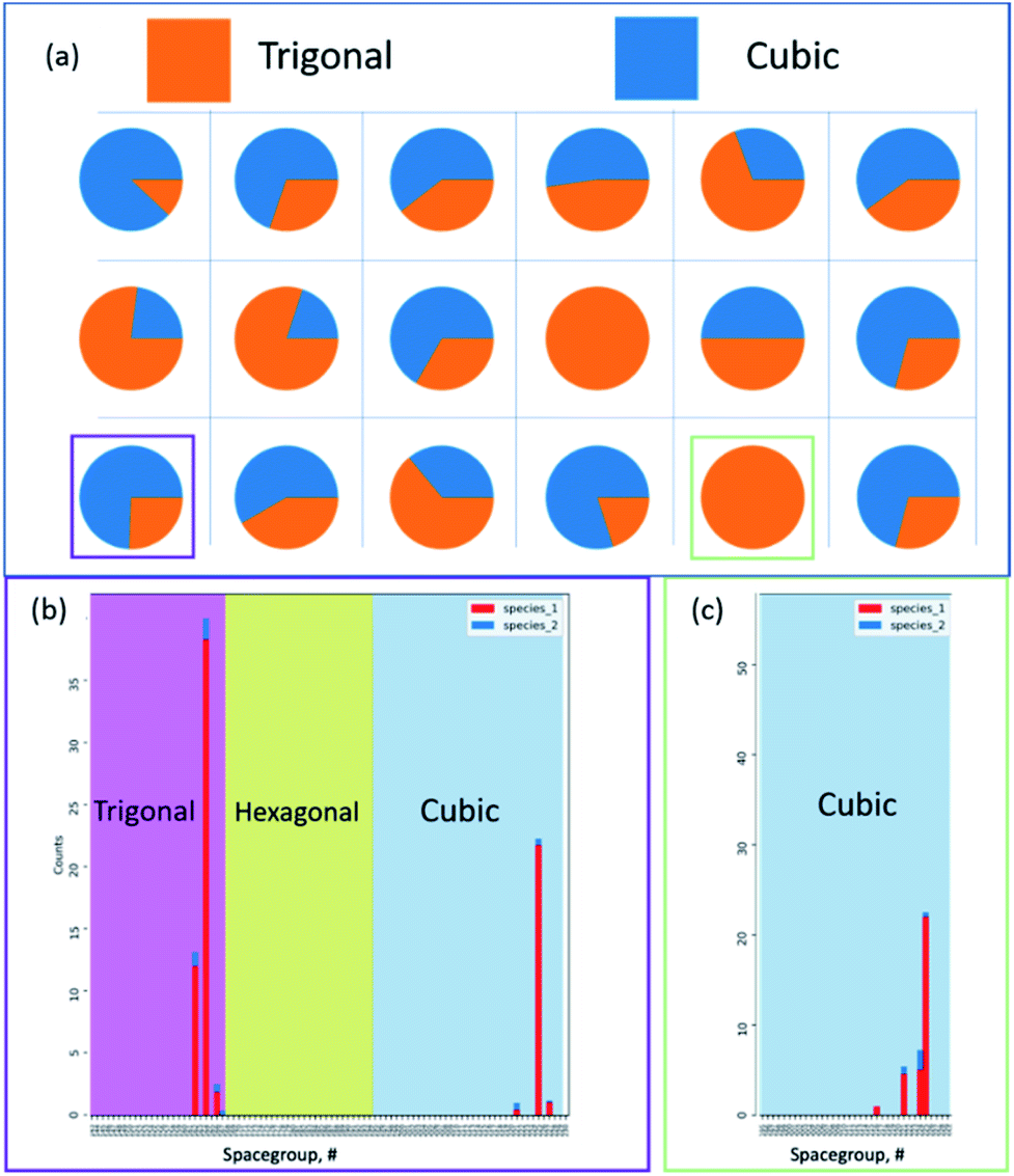 | ||
| Fig. 18 Detailed crystal chemistry analysis of multidimensional microscopy data. (a) Applying the convolutional neural network-based crystal model by Aguiar et al. we report the overall crystallographic family classification per pixel using up to six peaks for each diffraction pattern. Without a priori knowledge, the calculated per pixel classification provides an underlying crystal family level prediction, reporting the most prominent phase. Following this overarching classification, the underlying predictions for the crystal family are supported by points and, eventually, space groups based on selecting the two super pixels that are outlined in purple and green. Comparing the pixels, both (b) cubic and trigonal families are strongly predicted, and the all cubic families in (c) highlight the predictive and hierarchical model nature. At the lowest granularity for the space group, each of these previous plotted distributions provides the prominence of the primary cubic and trigonal components based on the underlying space groups, respectively, for each family. | ||
It should be further noted that based on the predictive crystal model from the electron diffraction patterns alone can be extended to larger datasets, including for example in Fig. 19a, in which identifying the underlying family, point, and space group distribution is required at this scale. It should be noted that each sub-pixelated electron diffraction pattern exemplified in Fig. 19b is classified for 3 to 6 peak combinations, forming a distribution and multiple predictions per point. With an expressed need to quickly evaluate the data, the model translates each pattern in Fig. 19c into a prediction for the crystal family, point group, and space group. This follows the ability to translate data as shown in Fig. 19d over specific pixels, rows, or columns, as configured by the user. The data reported here are only simple examples of the many potential avenues for which the model has been applied and now provides a larger community with a predictive and scalable tool for translating raw structural data from either high-resolution atomic-scale images or diffraction into predictive structural phase information, not limited by specific models or prior expertise.
 | ||
| Fig. 19 Extension to large diffraction datasets. (a) Via extension, the method can be applied over larger datasets including more than the (b) individual patterns collected over a larger imaging space. (c) Based on the predictions for each diffraction pattern, a classification map for the crystal family, point group, or prominent space group can be calculated; in this case, a crystal family is reported. (d) Beyond single pixels, the analysis can be performed over rows or columns. Note that the space group is reported for each column aligned with the prior family classification. | ||
Leveraging the advances to develop a computer vision and artificial intelligence engine for translating crystallographic and structural data now presents the opportunity for automation and augmentation of synthesis and control over nanostructured and nanoscale materials. Deep-learning models such as the one reported, have now been developed to circumvent classification, segmentation, and compression challenges. A limited number of these machine or deep-learning models have been proposed and have demonstrated sub-image sampling in image segmentation and inpainting over the fast to slow temporal regimes, allowing adaptive event tracking and augmentation over current microscope imaging, diffraction, and spectroscopic feeds. The main application being in situ microscopy, in which studying processes such as self-assembly, molecular organization, and catalysis, can be improved by the development of improved physics-based models by eliminating superfluous assumptions. Our temporal understanding associated with these processes is limited to a holistic understanding that is tied to the underlying fundamentals, including the effects of temperature, solution supersaturation, interfacial kinetics, and activation potential. The barrier to independent crystallographic structural determination has mainly been addressed. Now, the challenge is in translating the body of materials knowledge from the current databases into advanced and adaptive physics-informed workflows that are not limited to high-resolution electron microscopes and diffractometers used to study the nanoscale phenomenon.
Conclusions
Electron diffraction methods applied to materials in the size-ranges of tens or hundreds of nanometers have been used for several decades to characterize the crystalline structures of solids. This review presents advanced methods of electron diffraction that can be applied to metallic clusters (few nanometers) and nanoparticles. The complementary methods of characterization for metallic clusters and particles that are used to measure their properties are linked to their sizes, shapes, and crystalline structures. In this review we have discussed advanced methods of electron diffraction, emphasizing the significant potential of this technique. Most of our examples have involved Au clusters; however, the methods are equally valid for other metals and their alloys. Electron diffraction methods relating to TEM are still being developed. The main challenge for the future is to reduce the acquisition time and, therefore, the radiation damage to the cluster; it is particularly important to assure the integrity of the capping ligand. If the capping ligand is damaged, the cluster will become unstable and atomic rearrangements can occur that will alter the results. One possible improvement will be to pulse the beam to reduce the residence time. Additionally, large data sets are required to improve structural analysis. This field therefore still faces challenges, but the future is bright.Conflicts of interest
All authors declare that they have no competing interests.Acknowledgements
AP gratefully acknowledges financial support provided by the Department of Defense W911NF-18-1-0439 as well as the VPREDKE-T2 project at UTSA. This work was partially funded by MIRA -NAU with a seed grant. J. A. A. and J. T. performed the diffraction analysis, contributed figures, drafted the section on data analytics, and reviewed the entire manuscript. The authors acknowledge several contributors for providing samples for analysis: D. Sanchez, P. Parajuli, R. Mendoza, M. Hoque, J. J. Velazquez-Salazar, S. Vergara, A. Dass, and P. Horta.References
- P. Chakraborty, A. Nag, A. Chakraborty and T. Pradeep, Acc. Chem. Res., 2019, 52, 2–11 CrossRef CAS.
- T. Higaki, Y. Li, S. Zhao, Q. Li, S. Li, X.-S. Du, S. Yang, J. Chai and R. Jin, Angew. Chem., Int. Ed., 2019, 58, 8291–8302 CrossRef CAS.
- E. A. Doud, A. Voevodin, T. J. Hochuli, A. M. Champsaur, C. Nuckolls and X. Roy, Nat. Rev. Mater., 2020, 5, 371–387 CrossRef.
- A. Dass, J. Am. Chem. Soc., 2011, 133, 19259–19261 CrossRef CAS.
- F. Baletto and R. Ferrando, Rev. Mod. Phys., 2005, 77, 371–423 CrossRef CAS.
- R. Jin, Nanoscale, 2015, 7, 1549–1565 RSC.
- J. Yang and R. Jin, ACS Mater. Lett., 2019, 1, 482–489 CrossRef CAS.
- X. Kang and M. Zhu, Chem. Soc. Rev., 2019, 48, 2422–2457 RSC.
- Q. Tang, G. Hu, V. Fung and D.-e. Jiang, Acc. Chem. Res., 2018, 51, 2793–2802 CrossRef CAS.
- Y. Watanabe, Sci. Technol. Adv. Mater., 2014, 15, 063501 CrossRef.
- P. D. Jadzinsky, G. Calero, C. J. Ackerson, D. A. Bushnell and R. D. Kornberg, Science, 2007, 318, 430–433 CrossRef CAS.
- M. W. Heaven, A. Dass, P. S. White, K. M. Holt and R. W. Murray, J. Am. Chem. Soc., 2008, 130, 3754–3755 CrossRef CAS.
- N. K. Chaki, Y. Negishi, H. Tsunoyama, Y. Shichibu and T. Tsukuda, J. Am. Chem. Soc., 2008, 130, 8608–8610 CrossRef CAS.
- K. M. Harkness, Y. Tang, A. Dass, J. Pan, N. Kothalawala, V. J. Reddy, D. E. Cliffel, B. Demeler, F. Stellacci, O. M. Bakr and J. A. McLean, Nanoscale, 2012, 4, 4269–4274 RSC.
- D. B. Williams and C. B. Carter, Transmission Electron Microscopy, Springer US, 2009 Search PubMed.
- A. Avilov, K. Kuligin, S. Nicolopoulos, M. Nickolskiy, K. Boulahya, J. Portillo, G. Lepeshov, B. Sobolev, J. P. Collette, N. Martin, A. C. Robins and P. Fischione, Ultramicroscopy, 2007, 107, 431–444 CrossRef CAS.
- S. Nicolopoulos, A. Kuligin, K. Kuligin, B. Khalid, G. Lepeshov, J. L. DelPlancke, A. Avilov, M. Nickolsky and A. Ponce, Electron Crystallography: Novel Approaches for Structure Determination of Nanosized Materials, 2006, vol. 211, pp. 169–280 Search PubMed.
- S. Vergara, U. Santiago, C. Kumara, D. Alducin, R. L. Whetten, M. J. Yacaman, A. Dass and A. Ponce, J. Phys. Chem. C, 2018, 122, 26733–26738 CrossRef CAS.
- S. Vergara, D. A. Lukes, M. W. Martynowycz, U. Santiago, G. Plascencia-Villa, S. C. Weiss, M. J. de la Cruz, D. M. Black, M. M. Alvarez, X. López-Lozano, C. O. Barnes, G. Lin, H.-C. Weissker, R. L. Whetten, T. Gonen, M. J. Yacaman and G. Calero, J. Phys. Chem. Lett., 2017, 8, 5523–5530 CrossRef CAS.
- S. Iijima and T. Ichihashi, Phys. Rev. Lett., 1986, 56, 616–619 CrossRef CAS.
- R. F. Egerton, P. Li and M. Malac, Micron, 2004, 35, 399–409 CrossRef CAS.
- K. Momma and F. Izumi, J. Appl. Crystallogr., 2011, 44, 1272–1276 CrossRef CAS.
- D. Bahena, N. Bhattarai, U. Santiago, A. Tlahuice, A. Ponce, S. B. H. Bach, B. Yoon, R. L. Whetten, U. Landman and M. Jose-Yacaman, J. Phys. Chem. Lett., 2013, 4, 975–981 CrossRef CAS.
- R. F. Egerton, Ultramicroscopy, 2013, 127, 100–108 CrossRef CAS.
- G. McMullan, A. T. Clark, R. Turchetta and A. R. Faruqi, Ultramicroscopy, 2009, 109, 1411–1416 CrossRef CAS.
- D. Weber, A. Clausen and R. E. Dunin-Borkowski, in Handbook on Big Data and Machine Learning in the Physical Sciences, 2018, pp. 83–120, DOI:10.1142/9789811204579_0005.
- E. Voelkl, R. Herring, B. Bammes and D. Hoyle, Microsc. Microanal., 2015, 21, 1951–1952 CrossRef.
- L. Zhou, J. Song, J. S. Kim, X. Pei, C. Huang, M. Boyce, L. Mendonça, D. Clare, A. Siebert, C. S. Allen, E. Liberti, D. Stuart, X. Pan, P. D. Nellist, P. Zhang, A. I. Kirkland and P. Wang, Nat. Commun., 2020, 11, 2773 CrossRef CAS.
- L. J. Shery Chang, J. Barthel, R. Dunin-Borkowski and C. Dwyer, in European Microscopy Congress 2016: Proceedings, 2016, pp. 769–770, DOI:10.1002/9783527808465.Emc2016.6971.
- J. P. Buban, Q. Ramasse, B. Gipson, N. D. Browning and H. Stahlberg, J. Electron Microsc., 2010, 59, 103–112 CrossRef CAS.
- E. Ortega, A. Ponce, U. Santiago, D. Alducin, A. Benitez-Lara, G. Plascencia-Villa and M. Jose-Yacaman, Adv. Struct. Chem. Imaging, 2016, 2, 22–27 Search PubMed.
- A. Mittelberger, C. Kramberger and J. C. Meyer, Ultramicroscopy, 2018, 188, 1–7 CrossRef CAS.
- P. Williams, Appl. Phys. Lett., 1987, 50, 1760–1762 CrossRef CAS.
- J. P. Mornirolli, P. Stadelmann, G. Ji and S. Nicolopoulos, J. Microsc., 2010, 237, 511–515 CrossRef.
- J. P. Morniroli, G. Ji and D. Jacob, Ultramicroscopy, 2012, 121, 42–60 CrossRef CAS.
- P. A. Stadelmann, Ultramicroscopy, 1987, 21, 131–145 CrossRef CAS.
- A. Gómez-Rodríguez, L. M. Beltrán-del-Río and R. Herrera-Becerra, Ultramicroscopy, 2010, 110, 95–104 CrossRef.
- E. Voelkl and A. Ponce, Microsc. Microanal., 2018, 24, 1462–1463 CrossRef.
- R. Vincent and P. A. Midgley, Ultramicroscopy, 1994, 53, 271–282 CrossRef CAS.
- M. Blackman and G. P. Thomson, Proc. R. Soc. London, Ser. A, 1939, 173, 68–82 CAS.
- E. F. Rauch and M. Véron, Microsc. Microanal., 2016, 22, 500–501 CrossRef.
- P. P. Das, S. Nicolopoulos and M. Gemmi, Acta Crystallogr., Sect. A: Found. Adv., 2017, 73, C983 Search PubMed.
- L. Yedra, P. Torruella, A. Eljarrat, A. D. Darbal, J. K. Weiss, F. Peiró and S. Estradé, Appl. Phys. Lett., 2014, 105, 053117 CrossRef.
- E. F. Rauch and M. Véron, Mater. Charact., 2014, 98, 1–9 CrossRef CAS.
- D. Viladot, M. Veron, M. Gemmi, F. Peiró, J. Portillo, S. Estradé, J. Mendoza, N. Llorca-Isern and S. Nicolopoulos, J. Microsc., 2013, 252, 23–34 CrossRef CAS.
- E. F. Rauch and M. Veron, Materialwiss. Werkstofftech., 2005, 36, 552–556 CrossRef CAS.
- F. Ruiz-Zepeda, D. Bahena, A. Ponce and D. I. Garcia-Gutierrez, in Advanced Transmission Electron Microscopy, ed. L. F. Deepak, M. Alcala and R. Arenal, Springer, Cham, 2015, ch. 2, DOI:10.1007/978-3-319-15177-9_2.
- Á. K. Kiss, E. F. Rauch and J. L. Lábár, Ultramicroscopy, 2016, 163, 31–37 CrossRef.
- U. Santiago, J. J. Velazquez-Salazar, J. E. Sanchez, F. Ruiz-Zepeda, J. E. Ortega, J. Reyes-Gasga, L. Bazan-Diaz, I. Betancourt, E. F. Rauch, M. Veron, A. Ponce and M. Jose-Yacaman, Surf. Sci., 2016, 644, 80–85 CrossRef CAS.
- J. M. Zuo and J. C. H. Spence, Advanced Transmission Electron Microscopy, Springer, New York, NY, 2017 Search PubMed.
- R. Mendoza-Cruz, D. Romeu, L. Bazan-Diaz, J. Enrique Samaniego, U. Santiago, A. Ponce and M. Jose-Yacaman, Cryst. Growth Des., 2017, 17, 6062–6070 CrossRef CAS.
- U. Santiago, J. J. Velázquez-Salazar, J. E. Sanchez, F. Ruiz-Zepeda, J. E. Ortega, J. Reyes-Gasga, L. Bazán-Díaz, I. Betancourt, E. F. Rauch, M. Veron, A. Ponce and M. José-Yacamán, Surf. Sci., 2016, 644, 80–85 CrossRef CAS.
- A. B. Shah, S. T. Sivapalan, B. M. DeVetter, T. K. Yang, J. Wen, R. Bhargava, C. J. Murphy and J.-M. Zuo, Nano Lett., 2013, 13, 1840–1846 CrossRef CAS.
- S. J. L. Billinge, J. Solid State Chem., 2008, 181, 1695–1700 CrossRef CAS.
- C. L. Farrow and S. J. L. Billinge, Acta Crystallogr., Sect. A: Found. Crystallogr., 2009, 65, 232–239 CrossRef CAS.
- M. M. Hoque, S. Vergara, P. P. Das, D. Ugarte, U. Santiago, C. Kumara, R. L. Whetten, A. Dass and A. Ponce, J. Phys. Chem. C, 2019, 123, 19894–19902 CrossRef CAS.
- C. Fernando, M. M. Hoque, J. Reyes Gasga and A. Ponce, Microsc. Microanal., 2019, 25, 1926–1927 CrossRef.
- M. M. Hoque, K. M. Mayer, A. Ponce, M. M. Alvarez and R. L. Whetten, Langmuir, 2019, 35, 10610–10617 CrossRef CAS.
- A. Stukowski, Modell. Simul. Mater. Sci. Eng., 2009, 18, 015012 CrossRef.
- D. R. G. Mitchell, Microsc. Res. Tech., 2008, 71, 588–593 CrossRef CAS.
- D. T. Tran, G. Svensson and C.-W. Tai, J. Appl. Crystallogr., 2017, 50, 304–312 CrossRef CAS.
- A. Hjorth Larsen, J. Jørgen Mortensen, J. Blomqvist, I. E. Castelli, R. Christensen, M. Dułak, J. Friis, M. N. Groves, B. Hammer, C. Hargus, E. D. Hermes, P. C. Jennings, P. Bjerre Jensen, J. Kermode, J. R. Kitchin, E. Leonhard Kolsbjerg, J. Kubal, K. Kaasbjerg, S. Lysgaard, J. Bergmann Maronsson, T. Maxson, T. Olsen, L. Pastewka, A. Peterson, C. Rostgaard, J. Schiøtz, O. Schütt, M. Strange, K. S. Thygesen, T. Vegge, L. Vilhelmsen, M. Walter, Z. Zeng and K. W. Jacobsen, J. Phys.: Condens. Matter, 2017, 29, 273002 CrossRef.
- Jmol: an open-source Java viewer for chemical structures in 3D, http://www.jmol.org/ Search PubMed.
- J.-M. Zhang, F. Ma and K.-W. Xu, Appl. Surf. Sci., 2004, 229, 34–42 CrossRef CAS.
- P. Juhas, C. L. Farrow, X. Yang, K. R. Knox and S. J. L. Billinge, Acta Crystallogr., Sect. A: Found. Adv., 2015, 71, 562–568 CrossRef.
- S. Banerjee, C.-H. Liu, J. D. Lee, A. Kovyakh, V. Grasmik, O. Prymak, C. Koenigsmann, H. Liu, L. Wang, A. M. M. Abeykoon, S. S. Wong, M. Epple, C. B. Murray and S. J. L. Billinge, J. Phys. Chem. C, 2018, 122, 29498–29506 CrossRef CAS.
- K. M. Ø. Jensen, P. Juhas, M. A. Tofanelli, C. L. Heinecke, G. Vaughan, C. J. Ackerson and S. J. L. Billinge, Nat. Commun., 2016, 7, 11859 CrossRef CAS.
- S. Banerjee, C.-H. Liu, K. M. O. Jensen, P. Juhas, J. D. Lee, M. Tofanelli, C. J. Ackerson, C. B. Murray and S. J. L. Billinge, Acta Crystallogr., Sect. A: Found. Adv., 2020, 76, 24–31 CrossRef CAS.
- L. D. Marks and J. P. Zhang, Ultramicroscopy, 1992, 41, 419–422 CrossRef.
- S. Jesse, B. J. Rodriguez, S. Choudhury, A. P. Baddorf, I. Vrejoiu, D. Hesse, M. Alexe, E. A. Eliseev, A. N. Morozovska, J. Zhang, L.-Q. Chen and S. V. Kalinin, Nat. Mater., 2008, 7, 209–215 CrossRef CAS.
- S. Jesse and S. V. Kalinin, Nanotechnology, 2009, 20, 085714 CrossRef.
- T. LaGrange, G. H. Campbell, J. D. Colvin, B. Reed and W. E. King, J. Mater. Sci., 2006, 41, 4440–4444 CrossRef CAS.
- M. S. Grinolds, V. A. Lobastov, J. Weissenrieder and A. H. Zewail, Proc. Natl. Acad. Sci. U. S. A., 2006, 103, 18427–18431 CrossRef CAS.
- V. A. Lobastov, R. Srinivasan and A. H. Zewail, Proc. Natl. Acad. Sci. U. S. A., 2005, 102, 7069–7073 CrossRef CAS.
- R. M. v. d. Veen, T. J. Penfold and A. H. Zewail, Struct. Dyn., 2015, 2, 024302 CrossRef.
- A. Yurtsever and A. H. Zewail, Proc. Natl. Acad. Sci. U. S. A., 2011, 108, 3152–3156 CrossRef CAS.
- A. H. Zewail, Science, 2010, 328, 187–193 CrossRef CAS.
- P. D. Nellist and S. J. Pennycook , Scanning Transmission Electron Microscopy, Springer-VerlagNew York, 2011 Search PubMed.
- N. Dellby, L. Krivanek, D. Nellist, E. Batson and R. Lupini, J. Electron Microsc., 2001, 50, 177–185 CAS.
- J. M. LeBeau, S. D. Findlay, L. J. Allen and S. Stemmer, Phys. Rev. Lett., 2008, 100, 206101 CrossRef.
- W. Li, K. G. Field and D. Morgan, npj Comput. Mater., 2018, 4, 36 CrossRef.
- F. Cappia, B. D. Miller, J. A. Aguiar, L. He, D. J. Murray, B. J. Frickey, J. D. Stanek and J. M. Harp, J. Nucl. Mater., 2020, 531, 151964 CrossRef CAS.
- J. A. Aguiar, M. L. Gong, R. R. Unocic, T. Tasdizen and B. D. Miller, Sci. Adv., 2019, 5, eaaw1949 CrossRef CAS.
- J. A. Aguiar, M. L. Gong and T. Tasdizen, Comput. Mater. Sci., 2020, 173, 109409 CrossRef CAS.
| This journal is © The Royal Society of Chemistry 2021 |