
Advances in materials and devices for mimicking sensory adaptation
Zihan
He
ab,
Dekai
Ye
a,
Liyao
Liu
a,
Chong-an
Di
 *a and
Daoben
Zhu
*a
*a and
Daoben
Zhu
*a
aBeijing National Laboratory for Molecular Sciences, CAS Key Laboratory of Organic Solids, Institute of Chemistry, Chinese Academy of Sciences, Beijing 100190, China. E-mail: dicha@iccas.ac.cn; zhudb@iccas.ac.cn
bSchool of Chemical Sciences, University of Chinese Academy of Sciences, Beijing 100049, China
First published on 18th August 2021
Abstract
Adaptive devices, which aim to adjust electrical behaviors autonomically to external stimuli, are considered to be attractive candidates for next-generation artificial perception systems. Compared with typical electronic devices with stable signal output, adaptive devices possess unique features in exhibiting dynamic fitness to varying environments. To meet this requirement, increasing efforts have been made focusing on developing new materials, functional interfaces and novel device geometry for sensory perception applications. In this review, we summarize the recent advances in materials and devices for mimicking sensory adaptation. Keeping this in mind, we first introduce the fundamentals of biological sensory adaptation. Thereafter, the recent progress in mimicking sensory adaptation, such as tactile and visual adaptive systems, is overviewed. Moreover, we suggest five strategies to construct adaptive devices. Finally, challenges and perspectives are proposed to highlight the directions that deserve focused attention in this flourishing field.
 Zihan He | Zihan He graduated with a BS degree in Materials Science and Engineering from the South China University of Technology in 2016 and an MS degree from Shanghai Jiao Tong University in 2019. She is currently pursuing her PhD in the Institute of Chemistry, The Chinese Academy of Sciences (ICCAS). Her research interests focus on organic bioelectronics. |
 Dekai Ye | Dekai Ye works as a postdoc in the Organic Solids Laboratory of the ICCAS. He finished his PhD study in Inorganic Chemistry from Shanghai Institute of Applied Physics, The Chinese Academy of Sciences, in 2019. Currently, his research focuses on organic bioelectronics. |
 Liyao Liu | Liyao Liu received her PhD degree from the Institute of Chemistry, The Chinese Academy of Sciences (ICCAS), in 2019, and joined the ICCAS as a technician. Her research interests are focussed on organic thermoelectric materials and devices. |
 Chong-an Di | Chong-an Di is a professor of Organic Solids Laboratory in the ICCAS. He finished his PhD study in Chemistry from the ICCAS, in 2008, and was appointed as a professor in 2016 at the ICCAS. Currently, his research focuses on the investigation of organic thin-film transistors and organic thermoelectrics. |
 Daoben Zhu | Daoben Zhu is a professor and director of the Organic Solids Laboratory in the Institute of Chemistry, CAS. He finished his graduate courses at the East China University of Science and Technology in 1968. He was selected as an academician of the CAS in 1997. His research interests include molecular materials and devices. |
1. Introduction
Driven by the rapid development of artificial intelligence, smart devices that can mimic and even exceed the perception capabilities of human beings have attracted increasing attention.1–3 So far, there are two kinds of artificial perception-related devices being widely studied. The first category is used to detect target biological substances or physiological signals, which serve as electronic sensors for signal transduction.4–9 Another category of devices can simulate biological functions.10–20 The existing efforts have been focused on synaptic devices and have led to different kinds of neuromorphic elements. Although these devices can combine together to enable artificial perception elements, the integrated devices cannot exhibit adaptation abilities like those in biological systems. Under this circumstance, it is highly desirable to develop adaptive devices – which exhibit dynamic fitness to environmental conditions – that can automatically adjust their response to varying stimuli.“Survival of the fittest” is a basic biological concept of natural adaptation. All living systems, from a single cell to multicellular organisms and populations of interacting species,21 have the ability to adapt to changes in their environments.22,23 Humans have also evolved over time to develop the five exquisite sensory systems, which enable us to see, hear, taste, smell and touch for the vibrant perception of and complex interactions with the world. Every biological sensory system begins with a receptor that responds to physical stimuli to initiate a sensation.24 All sensory receptors have a form of adaptation to constantly detect changes in environments, which enables weak sensory inputs to be amplified and protected from noise while preventing strong inputs from saturating neural responses.25
Along with the booming development of artificial perception systems,1,26–29 adaptive devices have attracted significant interest for human–machine interfaces, physiological simulation, and prosthetic applications.30–32 The construction of adaptive devices typically requires devices in which information processing capability is merged with sensing ability to external stimuli. Historically, complementary metal–oxide–semiconductor (CMOS) circuits have played an important role in mimicking sensory adaptation since the 1990s.33,34 These silicon-based circuits often comprise several tens to hundreds of transistors and capacitors, leading to complicated logic designs. Recently, organic semiconductors (OSCs) have attracted increasing interest owing to their intrinsic features of good flexibility, solution processability, biocompatibility, etc.35 Based on these unique properties, a series of OSC-based devices, including organic electrochemical transistors (OECTs),36 tactile adaptation elements,37–43 organic adaptive transistors (OATs),30 and organic active adaptation transistors (OAATs),44 have been developed (Fig. 1). As a most recent example, our group developed an OAAT that possesses active visual adaptation ability to changeable light irradiation like human beings.44 These achievements boost the rapid development of this emerging area.
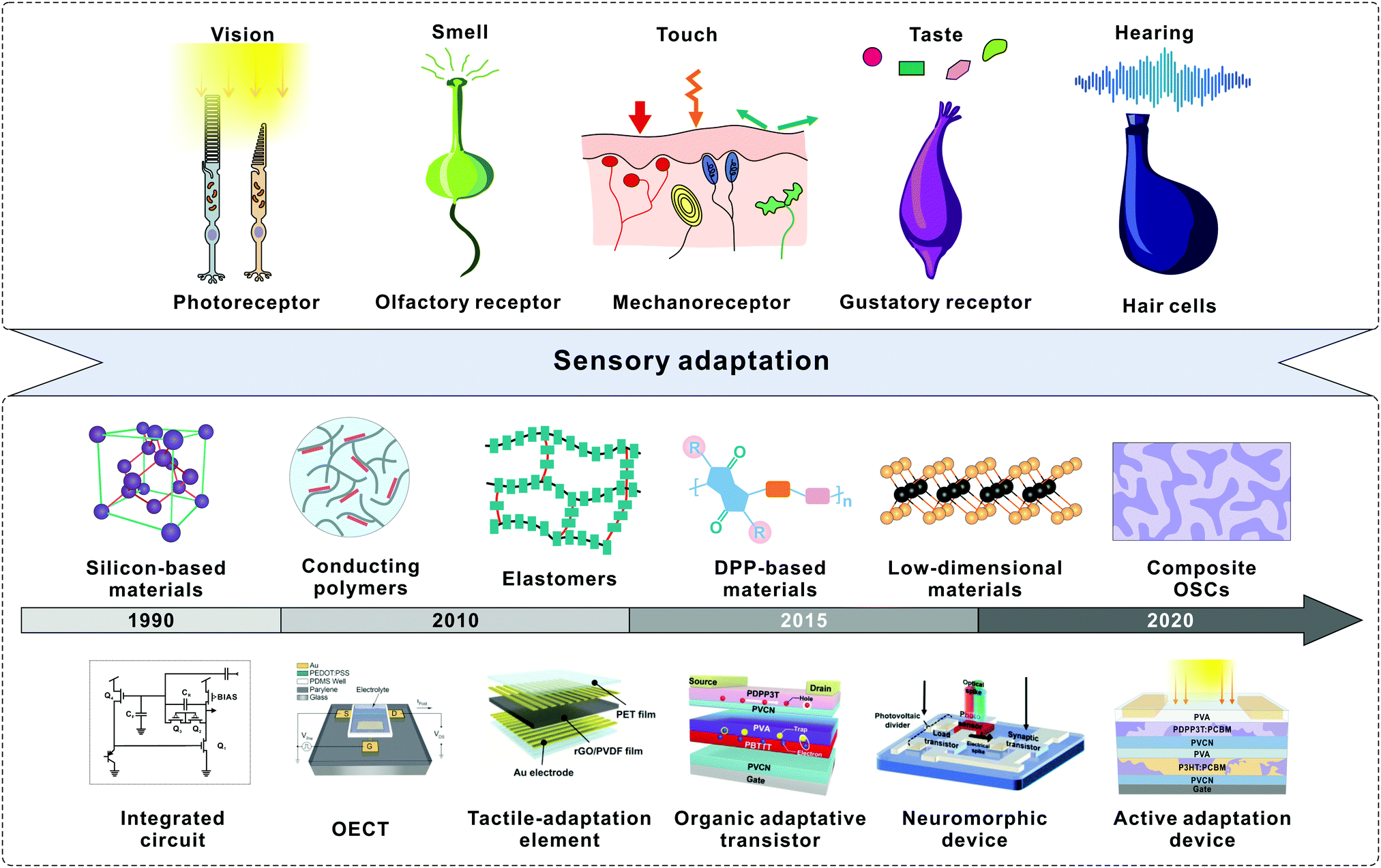 | ||
| Fig. 1 Development of sensory adaptation materials and devices. The top illustration shows the sensory receptors that enable fitness to various environmental stimuli including light, smell, force, taste, and sound. The bottom timeline shows the key advances in the rapid development of diverse adaptive devices. In the 1990s, silicon-based integrated circuits were developed to mimic adaptive photoreceptors. In terms of conducting polymers, adaptive devices based on OECTs were developed in 2015. Reproduced with permission.36 Copyright 2015, Wiley-VCH. Park et al. fabricated a tactile-adaptation element based on an elastomer. Reproduced with permission.37 Copyright 2015, The Authors. In 2019, an organic adaptive transistor was developed based on DPP-based materials. Reproduced with permission.30 Copyright 2019, Wiley-VCH. A light-adjustable neuromorphic circuit was introduced to mimic visual adaptation. Reproduced with permission.31 Copyright 2019, Wiley-VCH. We created an OAAT by utilizing composite OSCs. Reproduced with permission.44 Copyright 2021, Springer Nature. | ||
Along with the aforementioned developments, several strategies centring on functional materials,45,46 operating mechanisms32,47,48 and device architectures30 have been proposed to develop adaptive devices. However, there is no review focusing on the materials and device engineering of sensory adaptation. Here, we provide the recent progress in and perspective for adaptive electronics. We start with a brief introduction to sensory adaptation. Second, representative advances of sensory adaptation-inspired devices, including tactile-adaptive systems and visual-adaptive systems, are reviewed. We then present strategies to construct state-of-the-art adaptive devices. Finally, we suggest directions to stimulate more research interests in this intriguing area.
2. Fundamentals of sensory adaptation
We first introduce the biological adaptation behaviours to provide a fundamental understanding of adaptive devices. Biological sensory systems adjust their input–output relation according to external stimuli.23,49 A common phenomenon is a decrease in the gain of response to a continuous input; this is called sensory adaptation.50 When a stimulus is applied to sensory receptors and its final intensity is maintained at a stable level, the receptor responds with a series of action potentials, the frequency of which is initially high and then decreases. For humans, there are five categories of receptors (photoreceptors, olfactory receptors, mechanoreceptors, gustatory receptors and hair cells) responsible for sensory adaptation. For instance, mechanoreceptors exhibit different adaptive characteristics to external stimuli. Slow adapting (SA) receptors are sensitive to static pressure or touch and can produce a sustained signal in response to sustained stimuli. In contrast, fast adapting (FA) receptors can detect dynamic vibrations or sliding only at the beginning or end moments of the stimulation.39,51 As another example, photoreceptors adapt to background illumination, in order to amplify weak sensory inputs and prevent strong inputs from saturating.25 As a result, light adaptation allows eyes to quickly adapt to strong light,52,53 while dark adaptation enables the recovery of sensitivity in the dark.To date, two network topologies have been proposed to understand the mechanism of sensory adaptation.54–56 The first model indicates that adaptation comes from a negative feedback loop (NFL), and such adaptation is based on the integral of the difference between the desired and achieved responses. Based on this network motif, previous studies of adaptation devices are focused on designing error-correction-based feedback circuits, and have led to a wide range of applications in brightness and exposure control. The second class of models assumes that adaptation results from an incoherent feedforward loop (IFFL). This model posits that adaptation results from two complementary processes of excitation and inhibition that together regulate a response regulator. In fact, both NFL and IFFL models are indispensable in biological systems to realize dynamic adaptation.
Several key parameters are proposed to evaluate the adaptation abilities. Sensitivity is defined as the height of output response relative to the initial steady-state value, which reflects the largest transient relative change of the output divided by the relative change of the input.57 The decay constant (τ) is another parameter because it determines the timescales of the adaptation process, and the decay in firing rate can be described by a power-law relationship. T is the time at which the quantity is reduced to 1/e times of its initial value. Notably, the rate of adaptation differs widely in different sensory receptors. For example, four distinct types of mechanosensitive response can be classified as rapidly adapting (∼3–6 ms), intermediately adapting (∼15–30 ms), slowly adapting (∼200–300 ms) and ultra-slowly adapting modes (∼1000 ms).58 In photoreceptors, brief timescales reveal a rapid decay (∼30 ms) whereas a more prolonged decay constant (2–60 s) reveals a slower process.59 As adaptation allows sensory systems with an autonomic response to varying environments, it is vital to evaluate the response change relative to the external stimuli. We defined the active adaptation index (AAI) as the response change in the adaptation process relative to the increase of orders of luminance magnitude.44 For our OAAT, the AAI reaches its maximum value of 12.4 at the luminance of 105–106 cd m−2. The performance is consistent with that estimated from human beings.
3. Progress in sensory adaptation devices
To develop adaptive devices, several aspects should be taken into consideration. Take the existing organic adaptive transistors for example.30 Both stable and high mobility charge transport are required in the conductive channel, whereas charge trapping is indispensable in the dielectric layer. As a result, organic semiconductors with high mobility and fine-tuned energy levels relative to the dielectric layer are of vital importance. As for tactile-adaptation elements,37,38,40–42 applying external forces on the devices leads to variation in the signal output. Thus, several soft polymers with structural elasticity, chemical stability, piezoelectricity, etc. may have great potential for constructing adaptive devices. For mimicking visual adaptation, such as reported OAATs,44 prominent charge transport and efficient photocarrier generation are required in the photoresponsive active layer. As a result, the development of multifunctional materials and the design of unique device geometry are of significant importance. Fig. 2 displays the molecular structures of the mentioned materials in this review, including OSCs,30,44 conductive polymers,36 soft materials,37,38,40,43etc. Based on these materials, we summarize the recent progress in the development of tactile and visual adaptive systems.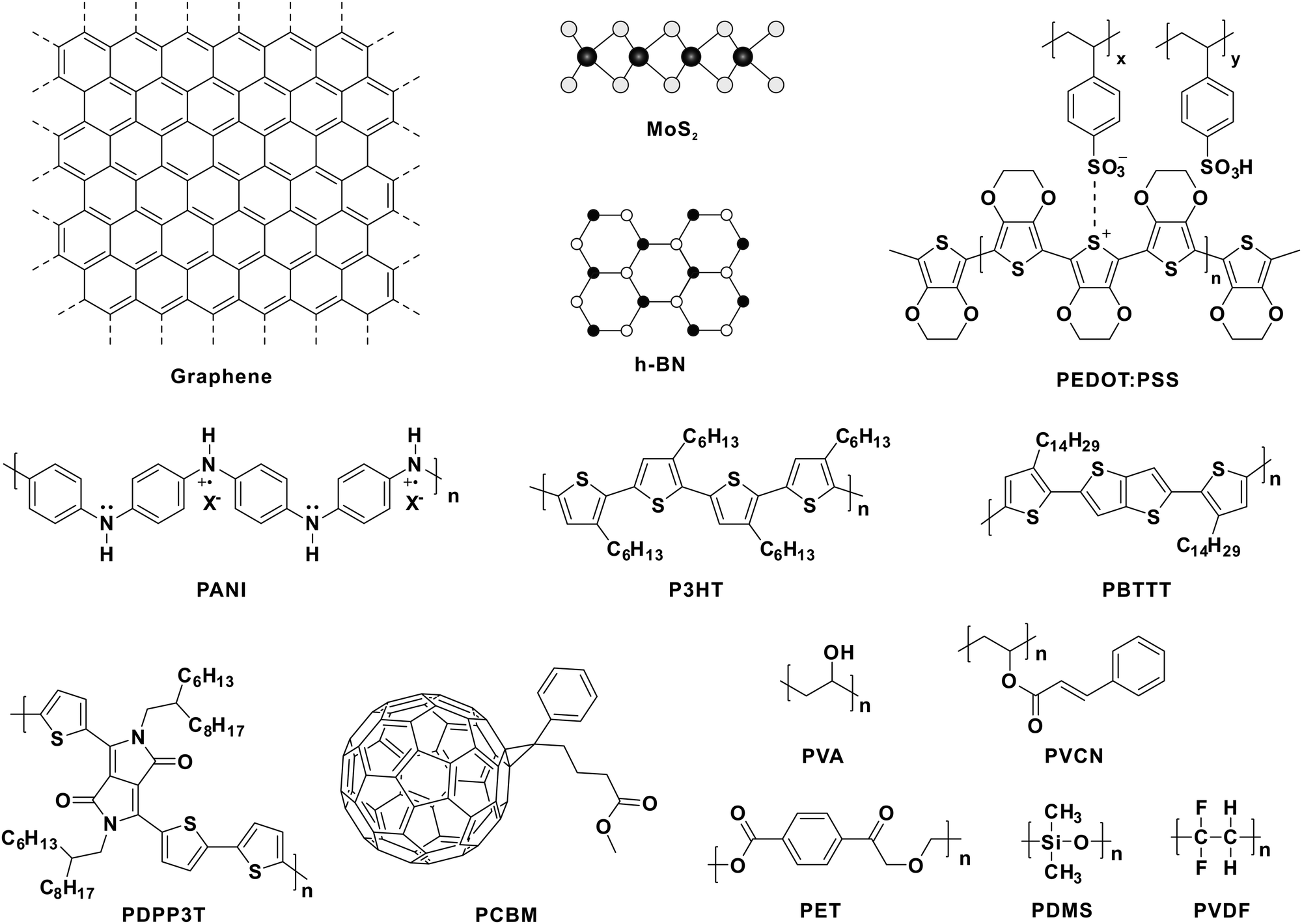 | ||
| Fig. 2 Molecular structures of materials discussed in this review. | ||
3.1. Tactile-adaptive system
To construct artificial tactile-adaptive systems, it is important to understand the key factors that affect the adaptation properties. As mentioned above, tactile adaptation is enabled by the combined efforts of various mechanoreceptors. Typically, there are four mechanoreceptors in the human skin that adapt quickly and slowly: Meissner corpuscle (MC), Merkel disk (MD), Ruffini cylinder (RC) and Pacinian corpuscle (PC).60 While MDs and RCs show the characteristics of SA, PCs and MCs show the characteristics of FA (Fig. 3a). Basically, adaptation is enabled by ion channel-gating in biological systems.30,58 When a sustained stimulus is applied, the ion channel is activated and then gradually inactivated, with recovery after the removal of the stimulus (Fig. 3b). As a result, the response of mechanoreceptors gradually decreased and was then maintained at a stable level during the adaptation process (Fig. 3c). In order to mimic the tactile-adaptation characteristics, it is essential to develop an element that can imitate both SA and FA behaviors as human receptors.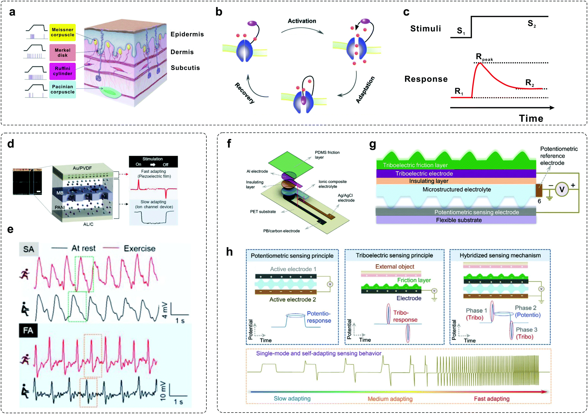 | ||
| Fig. 3 Examples of mimicking tactile-adaptive systems. (a) Anatomy of the human tactile sensory system. Four mechanoreceptors in the human skin: Meissner corpuscle (MC), Merkel disk (MD), Ruffini cylinder (RC), and Pacinian corpuscle (PC). Reproduced with permission.60 Copyright 2019 Elsevier B.V. (b) Schematic illustration of the sensory adaptation process in bio-systems.30,58 When a maintained stimulus is loaded, the channel is activated and then gradually inactivated within a timescale of τ, with recovery after the removal of the stimulus. (c) Input–output curve defining sensory adaptation. Generally, the output response decreased dynamically under sustained stimuli, allowing the sensory neurons with high sensitivity to a wide range of stimuli input. (d) A self-powered sensor mimicking slow- and fast-adapting mechanoreceptors. (e) Two characteristic signals in the form of SA and FA before (black) and after (red) exercise. Reproduced with permission.41 Copyright 2018, Wiley-VCH. (f) Illustration showing the structure of a single-mode, self-adapting mechanoreceptor. (g) Schematic of the configuration design of the mechanoreceptor. (h) Schematic diagrams of the device in the potentiometric, triboelectric, and hybridized sensing modes. Reproduced with permission.43 Copyright 2020, Wiley-VCH. | ||
Han et al. developed a self-powered artificial mechanoreceptor by spatially integrating a piezoelectric film and an ion channel system into one device (Fig. 3d).41 The device is fabricated with an electrode (Al/C), an electrolyte (polyaniline (PANI) solution), a pore membrane (MB) and a piezoelectric film (Au/PVDF). When the device is pressed and released, ion movement in the PANI is observed through the polycarbonate track-etched MB, thus mimicking SA signals, while the signal generated from the connection between the upper part of the Au/PVDF and the Al/C exhibits the characteristics of FA. Both the functions of FA and SA can be accomplished simultaneously, and typical adaptation signals in the rest and exercise states can be observed under repeated stimuli (Fig. 3e). Recently, Arias et al. demonstrated a single-mode mechanoreceptor based on a potentiometric–triboelectric hybridized configuration (Fig. 3f and g) that exhibits self-adapting behaviours.43 The device can be regulated from slow adapting to medium adapting and fast adapting mode according to the external stimuli (Fig. 3h). In addition, such a device can also adapt to diverse mechanical characteristics, including magnitude, frequency, duration, applying and releasing speed, for resolving complex stimuli.
In biological sensory systems, tactile stimuli are converted into action potentials and then transmitted via afferent nerves. In previous reports, pressure information can be converted into voltage pulses using ring oscillators.61,62 Recently, an artificial neural tactile sensing system that can mimic SA and FA mechanoreceptors, as well as generate sensory neuron-like signals, was demonstrated.47 The tactile skin (T-skin) films were fabricated by incorporating FA-mimicking BaTiO3 nanoparticles and SA-mimicking reduced graphene oxide (rGO) sheets in an elastic polymer matrix, enabling a sensitive response to static pressure and vibration simultaneously (Fig. 4a). The SA sensors produce piezoresistive responses under static pressure (0.1–100 kPa), which matches well with the typical human perception range (Fig. 4b).63 And, even high-frequency vibrations of 1000 Hz that exceed the human vibration detection range can be achieved in FA sensors (Fig. 4c).64 Furthermore, the SA- and FA-type neural signal patterns similar to real tactile nerve signals can be generated using an artificial mechanoreceptor neural (AMN) board. Such SA or FA neural simulator signals can be fully transmitted in real nerves or can activate the hindlimb muscles (Fig. 4d and e). Recently, we developed an OAT with fine-tuned adaptation functionality.30 Interestingly, the adaption speed can be modulated from ultraslow to fast adaptation through dielectric engineering. Notably, the FA-OAT has been utilized to construct an artificial tactile circuit. The effective detection of pressure onset and offset in this circuit was stimulated successfully based on the FA-on and FA-off device, respectively.
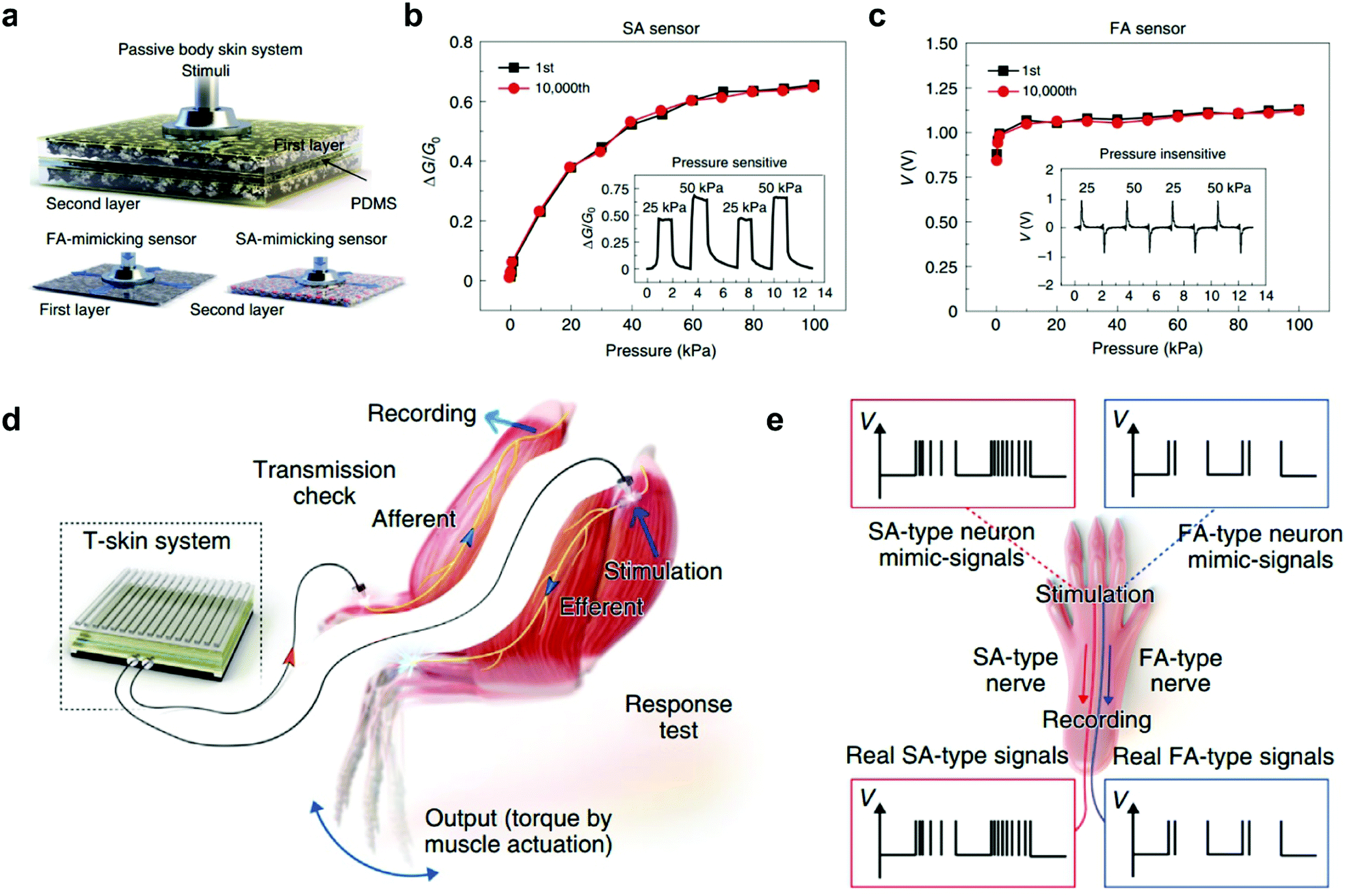 | ||
Fig. 4 An artificial neural tactile sensing system. (a) Configuration of a T-skin sensor for a passive body skin system. The first layer is a BaTiO3-enriched FA-mimicking sensor whereas the second is an rGO-enriched SA-mimicking sensor. (b and c) SA and FA sensor responses under static pressure (0.1–100 kPa) in 10![[thin space (1/6-em)]](https://www.rsc.org/images/entities/char_2009.gif) 000 repeated measurements. The insets depict the piezoresistive and piezoelectric responses under dynamic pressure inputs (25 and 50 kPa). (d) A schematic of ex vivo and in vivo experiments for T-skin applications. (e) Simulation and recording procedures in SA- and FA-type nerves. Reproduced with permission.47 Copyright 2021, Springer Nature. 000 repeated measurements. The insets depict the piezoresistive and piezoelectric responses under dynamic pressure inputs (25 and 50 kPa). (d) A schematic of ex vivo and in vivo experiments for T-skin applications. (e) Simulation and recording procedures in SA- and FA-type nerves. Reproduced with permission.47 Copyright 2021, Springer Nature. | ||
3.2. Visual-adaptive system
Studies from neuroscience and cognitive psychology have revealed that more than 80% of the information from the outside world reaches the brain through vision.65 The environmental light intensity ranges over ten orders of magnitude in our daily life, whereas the firing rate of optical nerve fibres spans less than two.66,67 The existing gap between the light stimulus and processable signal is filled by the visual adaptive system, where an active shift of visual threshold and sensitivity occurs according to the luminance backgrounds. Notably, this biological functionality is achieved via a coupled physiological mechanism, that is, pupil constriction, photo-pigment depletion, and receptor depression, to enable both sensitive response to dim lights and automatic depression to high brightness stimuli. To meet these requirements, photoadaptive devices with fine-tuned sensitivity are in demand. In modern electronics, self-adaptive optical regulation systems with automatic brightness and exposure control functionality have been applied, but they cannot match the adaptation behaviors in bio-systems. Recently, numerous efforts have been made to achieve this goal. An environment-adaptable optoelectronic circuit array that emulates biological visual functionalities can be used to achieve bionic visual perception (Fig. 5a).31 The function of light adaptation was emulated by integrating a CdSe photosensor, an IGZO load transistor and a metal oxide synaptic transistor. In this device, the visual threshold to environmental light intensities can be controlled by the load gate bias (VL), where the visual image under bright light can be perceived by enlarging the VL, while weak light can be distinguished by decreasing the VL. Additionally, a 3 × 3-pixel array of neuromorphic circuits was fabricated to demonstrate the environment-adaptable pattern recognition features (Fig. 5b). As the intensity of light condition decreased, a high contrast ‘H’ image could be clearly discriminated because of lowering the load gate voltage (Fig. 5c and d). This system proves the feasibility of using adaptable devices in complicated environments.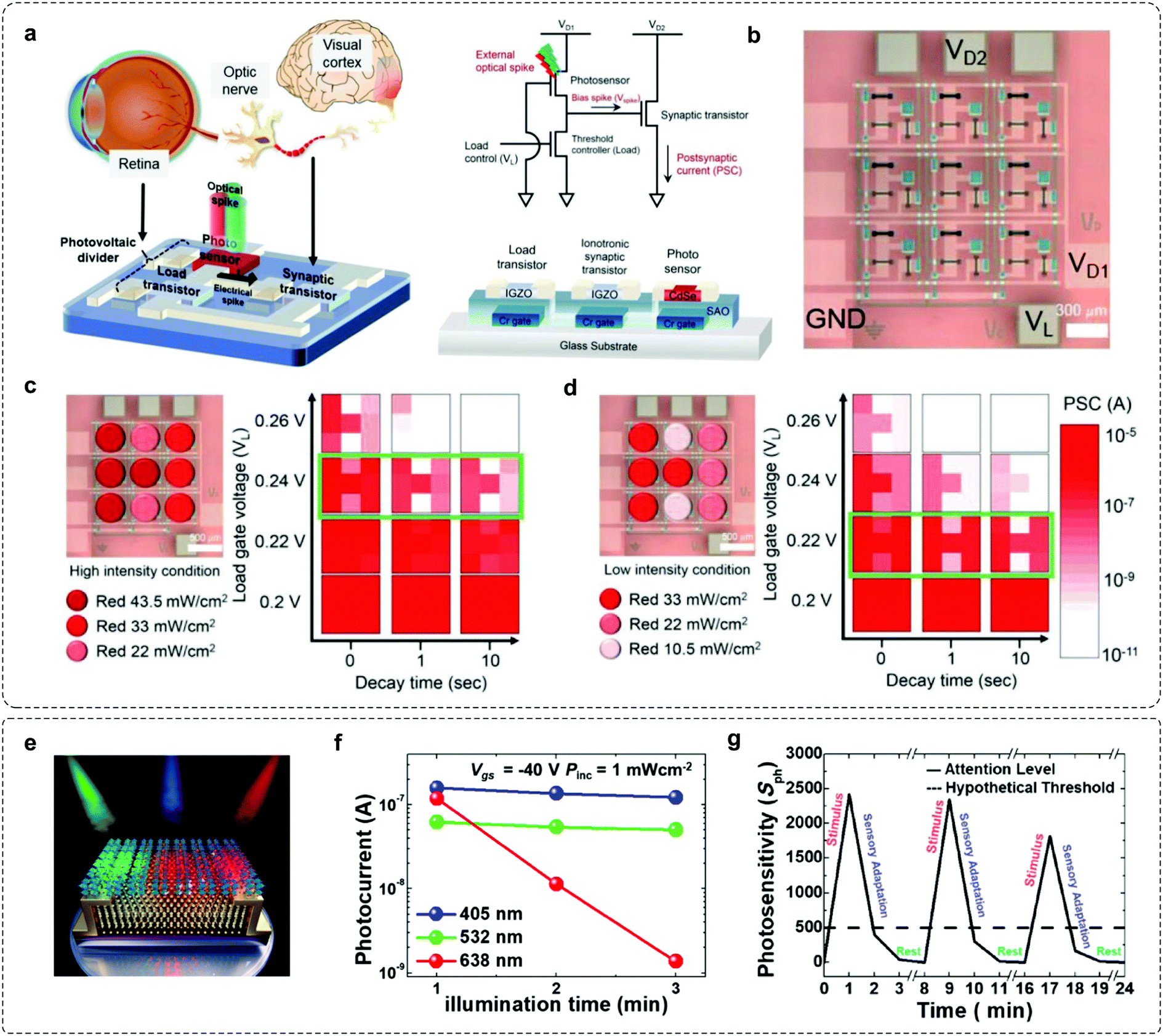 | ||
| Fig. 5 Examples for mimicking visual-adaptive systems. (a) A light-adjustable optoelectronic neuromorphic circuit consists of a photovoltaic divider (CdSe photosensor + a-IGZO load transistor) and an ionotronic synaptic transistor (a-IGZO TFT). (b) Optical microscopy image of a 3 × 3 optoelectronic neuromorphic circuit array; (c) under high-intensity (22–43.5 mW cm−2) and (d) low-intensity (10.5–33 mW cm−2), respectively. Reproduced with permission.31 Copyright 2019, Wiley-VCH. (e) Schematic illustration of the CsPb(Br0.5I0.5)3–MoS2 phototransistor. (f) Photocurrents of the perovskite–MoS2 phototransistor with respect to time under RGB light illumination. (g) Photosensitivity of the device emulating sensory adaptation. Reproduced with permission.32 Copyright 2020 American Chemical Society. | ||
Kim et al. developed a neuromorphic phototransistor based on the hybrid structure of CsPb(Br1–xIx)3 perovskite and MoS2 that exhibits selective red-adaptation (Fig. 5e).32 A gradually decreased IDS was observed under red light illumination (λ = 638 nm); here, the underlying mechanism is the halide phase segregation of the mixed halide perovskite, leading to iodide- and bromide-rich domains. As the energy of the red light was lower than that of the PL spectra for the bromide-rich domain, that is, energy band gap widening by the bromide-rich domain, significant photocurrent degradation was observed over time (Fig. 5f and g). This photosensory-adaptation behavior can be potentially applied to artificial intelligence and may pave a new way for color-selective adaptive elements. Having mentioned that, a breakthrough in mimicking visual adaptation is the creation of an OAAT.44 This device exhibits light intensity-dependent active photoadaptation, for light stimuli ranging over six orders of magnitude. This photoadaptation element is capable of mimicking dynamic visual adaptation behaviors. We will have a comprehensive description of this work in Section 4.4.
4. Strategies to construct sensory adaptation devices
Different perception conditions require varied categories of adaptive devices. However, all systems have much in common in terms of output signals, which generally exhibit dynamic responses under sustained stimuli. An ideal adaptive device should decline dynamically and controllably in response to sustained stimuli while maintaining long-term stability to repeated stimulations. Based on this nature, there are several strategies for constructing adaptive devices. Herein, we summarize five concepts for the design of adaptive devices.4.1. Enabling adaptation by manipulating the charge trapping–detrapping process
Charge trapping typically leads to unfavourable current decay and plays a negative role in determining stability in an electronic device. However, controllable decay represents an important feature for most adaptive devices. Consequently, fine-tuned charge trapping and detrapping processes can principally serve as a strategy to enable adaptation. Keeping this in mind, a recent work utilizing the charge trapping mechanism has been demonstrated based on a field-effect transistor (FET).45 The device is fabricated with a MoS2 semiconducting channel, hexagonal boron nitride (h-BN) tunnelling insulator, and graphene (Gr) floating gate (Fig. 6a). The underlying mechanism for the adaptation feature is ascribed to the occurrence of trapping events at the MoS2/h-BN interface,68 where the trapped electrons block the electric field from the gate, resulting in a smaller effective gate voltage. The output current degrades over time when the gate bias changes from 20 to 50 V (Fig. 6b), and such decreasing adaptation behaviour can also be observed under different amplitudes (Fig. 6c).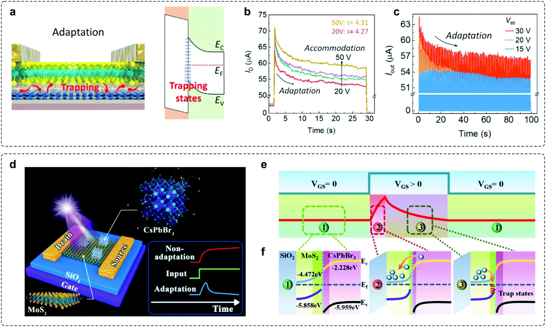 | ||
| Fig. 6 Adaptive transistors based on the charge trapping–detrapping mechanism. (a) Schematic illustrations of the working principles of adaptation characteristics and the corresponding energy-band diagram. (b) Time-dependent output curves under successive gate bias conditions. (c) The pulse response of the VS-FET. The device exhibits an adaptive response to multiple 0.2 s pulses. Reproduced with permission.45 Copyright 2021, Elsevier Inc. (d) A photoelectric adaptive device based on a 0D-CsPbBr3-QDs/2D-MoS2 mixed-dimensional heterojunction transistor. (e) A typical adaptation curve of the adaptive device can be divided into the initial state, activated process, and adaptive process, respectively. (f) Schematic illustrations of the energy-band diagram of the device. Reproduced with permission.46 Copyright 2021, Wiley-VCH. | ||
Another work based on the charge trapping–detrapping mechanism has been carried out based on a mixed-dimensional heterojunction transistor.46 The device is fabricated with a gated-modulated 0D-CsPbBr3-quantum-dots/2D-MoS2 heterostructure (Fig. 6d), and 2D-MoS2 was chosen as the bottom channel of the vertical heterojunction due to its controllable charge transport properties.69,70 The charge trapping–detrapping behavior is observed in the space charge region of the heterojunction (SCRH), resulting in the clear decay of IDS, which serves as the basic condition to mimic sensory adaptation (Fig. 6e and f).71 Upon the onset of positive VGS, a significant peak current is generated in a short time as a result of the rapid and effective accumulation of electrons in the conductive channel. Subsequently, the time-dependent electron-trapping phenomenon occurs in the SCRH formed between MoS2 and quantum-dots (QDs), leading to a clear decrease of IDS.72,73 This process corresponds to the typical adaptation behavior in biological systems. And, a rapid electron-detrapping phenomenon would result in an immediate recovery of the device performance after the removal of external stimuli, thus promoting the entire adaptation process. In addition, a series of adaptive behaviors, such as accuracy, sensitivity, inactivation and desensitization, have been successfully stimulated, implying promising applications in artificial intelligence and bionic robots.
4.2. Optimization of device geometry for controllable adaptation
As mentioned above, an adaptive device requires short-term decay in output current and prominent long-term stability in one device. These contradictory features make the construction of adaptive transistors particularly challenging, because of the paradoxical demands of excitation and inhibition to the charge transport in the same conductive channel. OFETs have been considered to be promising candidates in sensory systems.5,14,18,74–76 In an OFET, three terminals (gate, source and drain) are separated by semiconductor layers and dielectric layers. When a voltage is biased between the gate and semiconductor, carriers can be induced at the dielectric–semiconductor interface and form a conductive channel. Through molecular design and device engineering, OFETs can convert external stimuli, such as light or pressure into electrical signals,18,74,77,78 which provided the possibility to construct organic adaptive transistors. Of particular note, the variation in device geometry can affect the involved interfaces, charge transport pathway and trapping mechanism. As a result, device geometry is an important factor that affects the functionalities of OFETs.Our group demonstrated an OAT by introducing a composite dielectric layer (PVCN/PBTTT/PVA/PVCN) into the bottom-gate top-contact device (Fig. 7a).30 The inbuilt charge-trapping interface (PBTTT/PVA) in the PVCN dielectric layer endows the device with separated charge transport and a self-adaptive interfacial trapping process, which contribute to the unique volatile shielding of the gating field. It therefore led to rapid and temporary decay of the carrier concentration in the conductive channel without diminishing the charge transport ability, allowing independent manipulation of two contradictory processes. The applied VGS pulses induced a rapid and repeatable decay of the IDS (Fig. 7b), illustrating the rapid short-term decay and prominent long-term stability for mimicking sensory adaptation. Interestingly, by modulating the electron-trapping dielectric or semiconductor layer, the device exhibits a fine-tuned decay constant ranging from 50 ms to 5 s (Fig. 7c), precisely matching the adaptation timescales in biological systems.59,79,80 Based on such unique properties, OATs can be utilized to emulate many advanced adaptation behaviors to dynamic stimuli. For example, the SA-OAT exhibited a notable IDS response with the increase of VGS onset speed from 2.5 to 10 V s−1 (Fig. 7d and e). While applying a series of double-step VGS, OATs exhibited high sensitivity (from 30 to 12 V−1) when compared to non-adaptive devices (from 40 to less than 0.5 V−1), due to the biomimetic suppression of input background (Fig. 7f and g). By exploiting the prominent adaptive properties, OATs serve as a powerful tool to enable biomimetic perception elements.
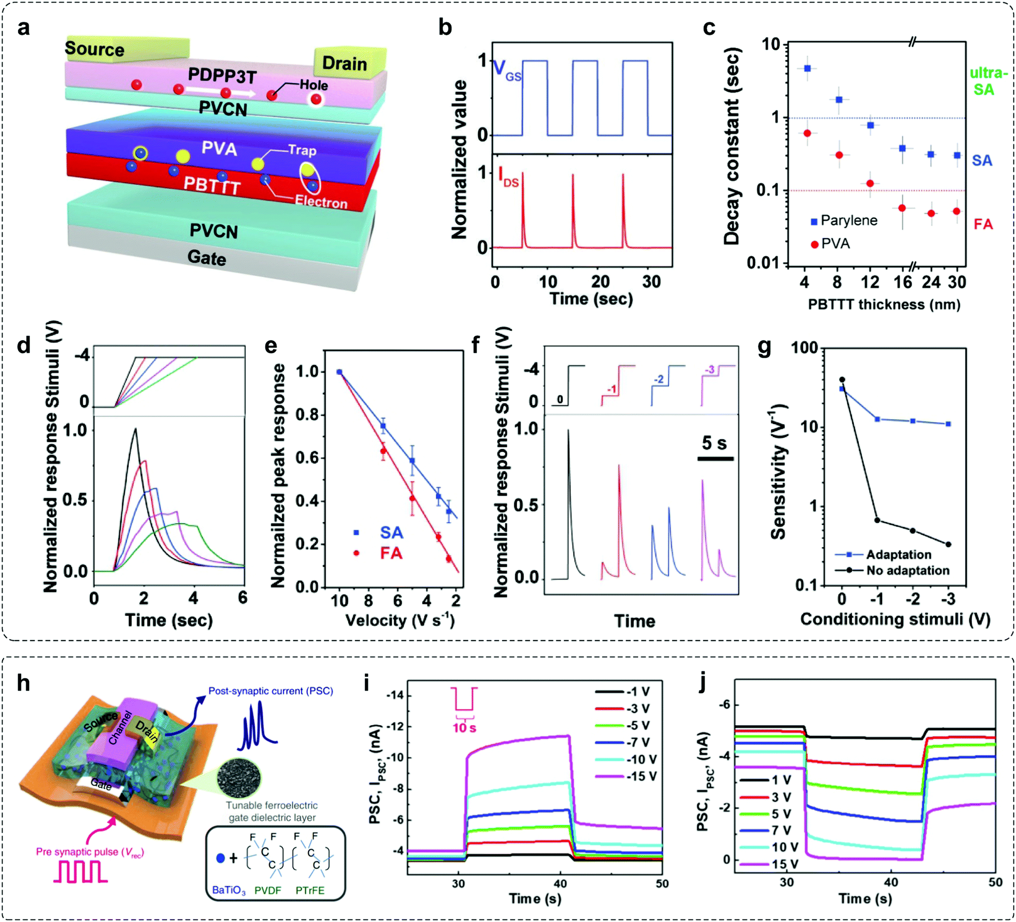 | ||
| Fig. 7 Examples of adaptive transistors with novel device geometry. (a) Schematic diagram of the proposed organic adaptive device. PBTTT/PVA is buried with the PVCN dielectric layer to facilitate adaptive electron trapping. (b) Time-dependent IDS response upon VGS pulses. The applied VDS and VGS were −1 and −4 V, respectively. (c) Fine-tuned decay constants of ultra-SA, SA, and FA devices as a function of PBTTT film thickness with PVA or parylene dielectrics. (d) Time-dependent response of SA-OATs with different onset speed of stimuli. (e) Peak response of SA- and FA-OATs as a function of onset speed of stimuli. (f) Response of SA-OATs to a periodically increased stimulus. (g) Correlation between sensitivity to the latter stimuli and conditioning stimuli. Reproduced with permission.30 Copyright 2019, Wiley-VCH. (h) Sketch of the device structure. Gate dielectric layer consists of BT NPs/P(VDF-TrFE) ferroelectric material. (i and j) Mimicking slowly adapting reception properties of the Fe-OFET. The output current of the device was recorded by applying a sustained potential of −10 V and 10 V with varying amplitude (∼10 s). Reproduced with permission.14 Copyright 2020, The Author(s). | ||
Recently, Lee et al. reported a flexible ferroelectric organic field-effect transistor (Fe-OFET) that can emulate the tactile sensory organ.14 This device is based on a ferroelectric nanocomposite gate dielectric layer of barium titanate nanoparticles (BT NPs) and poly(vinyledenedifluoride–trifluoroethylene) (P(VDF-TrFE)) (Fig. 7h). When tactile stimulation is applied to the gate electrode, the alignment of dipoles is induced in the ferroelectric gate dielectric layer by the triboelectric–capacitive coupling effect. The resulting output current exhibits an increasing tendency with a decreasing slope throughout simulation until equilibrium is reached (Fig. 7i and j), which is akin to the SA sensation of human beings.
4.3. Device integration for bio-inspired perception applications
In realistic applications, adaptive devices have to operate under various stimuli, in order to enable good processing of external stimuli in a changeable environment. To fulfil this demand, an adaptive element should combine the detection of external signals and dynamic response to environmental conditions. Since these functionalities can be hardly achieved in a single device, the effective integration of sensing elements with adaptive devices is desirable for realizing advanced adaptation applications.Integration of pressure sensors with OATs was carried out to verify the adaptation behaviours.30 The OAT integrated circuits exhibit high sensitivity and decreased power consumption, and can be utilized to mimic FA events as human mechanoreceptors. By integrating tactile and temperature sensors that communicate through the asynchronously coded electronic skin (ACES) pulse signatures,48 Tee's group designed a biomimetic model to mimic adaptation behaviours (Fig. 8a and b). Similar to biological counterparts,51 ACES-FA receptors respond to dynamic skin deformations as they transmit events immediately due to the increase (FA+) or decrease (FA−) in pressure, whereas ACES-SA receptors modulate static pressure intensity by event frequency. In addition, combining pressure- and temperature-sensitive transducers on a flexible substrate (Fig. 8c), simultaneous detection of thermotactile sensations could be achieved (Fig. 8d). The integration of different elements brings new opportunities for constructing multimodal devices with desired functionality. Arias et al. integrated the self-adapting mechanoreceptor with soft robotic hands to monitor real-time object manipulations (Fig. 8e).43 The entire robotic gripper can be actuated and controlled with compressed air when pressurized by external objects. From the recorded signal outputs of the integrated mechanoreceptor when manipulated with an apple, “pick-hold-place” can be clearly recognized as a result of the self-adaptive potentiometric–triboelectric hybridized sensing mode (Fig. 8f). The integrated soft robotic gripper is applicable for resolving complex stimuli with high accuracy, efficiency, and versatility in different sensing scenarios.
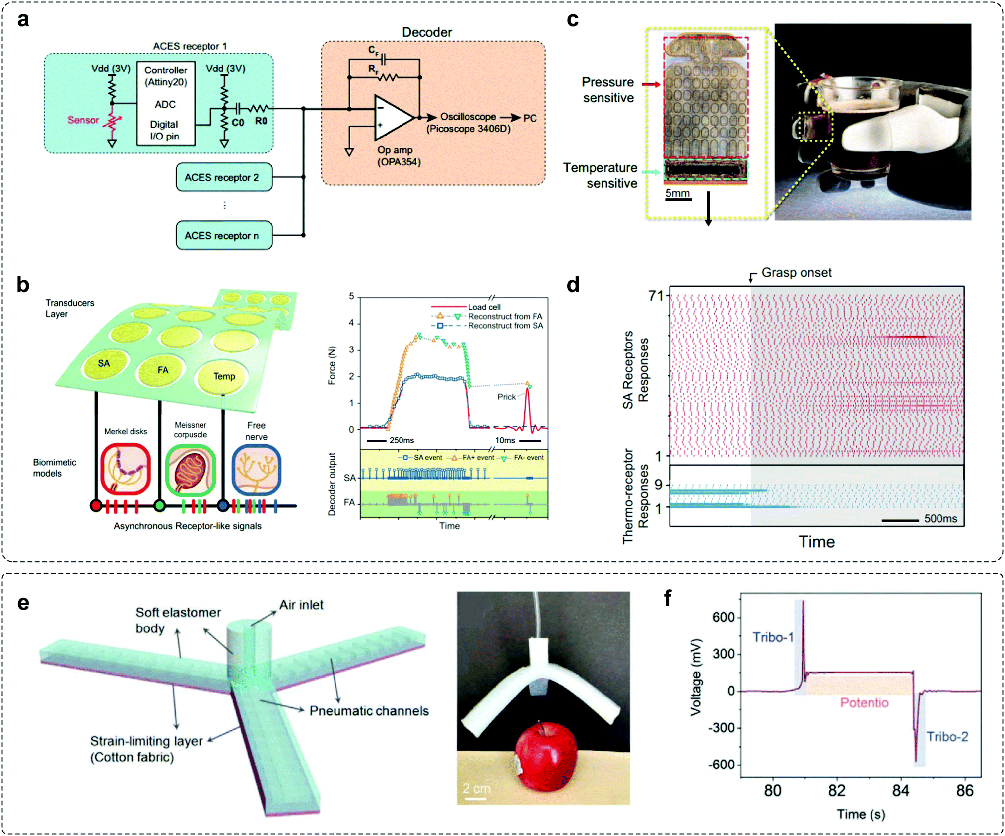 | ||
| Fig. 8 Integrated systems for adaptation applications. (a) The architecture of the ACES. Multiple receptors are connected to a decoder via a signal electric conductor. (b) A multimodal ACES sensor array that converts tactile stimuli to SA, FA+, or FA− events. (c) Photography of the flexible multimodal sensing e-skin integrated with pressure- and temperature-sensitive transducers. (d) SA receptor response (top) and temperature-sensitive (bottom) of the ACES receptors during the grasp. Reproduced with permission.48 Copyright 2019, The American Association for the Advancement of Science. (e) Soft robotic gripper with mechanoreceptors for the manipulation of the apple. (f) The signal output of the mechanoreceptor when performing “pick-hold-place” operations. Reproduced with permission.43 Copyright 2020, Wiley-VCH. | ||
4.4. Towards active adaptation triggered by external stimuli
An ultimate goal of adaptive devices relies on the achievement of active adaptation to enable an autonomic response to varying external stimuli. In fact, light irradiation can principally offer a powerful approach to modulate carrier concentration and even achieve active adaptation. Previous efforts have focused on achieving stable photocurrent generation for light detection.81,82 In contrast, a desired photoadaptive element must exhibit light intensity-dependent photoexcitation and inhibition functionalities in one device, in order to enable a direct response to stimuli.14,83 Under this circumstance, it is extremely challenging to design the so-called active adaptive devices with both transient photo-response and dynamic adaptation functionality.Of particular note, a similar conundrum has been overcome in biological visual systems by using the coupled physiological mechanism. The related transmembrane transport of two different ions (Na+ and Ca2+) together with the associated gating dynamics leads to biological active adaptation.54,84–87 This unique mechanism offers an inspiration to achieve coupled manipulation of charge carriers on an OFET toward photoadaptive transistors. Our group reported an OAAT that exhibits light intensity-dependent active photoadaptation, which successfully imitated advanced adaptation behaviours of biological visual systems.44 In this device, two functionally complementary bulk-heterojunctions are introduced in an OFET to function as the photoresponsive active layer and floating gate, respectively (Fig. 9a).
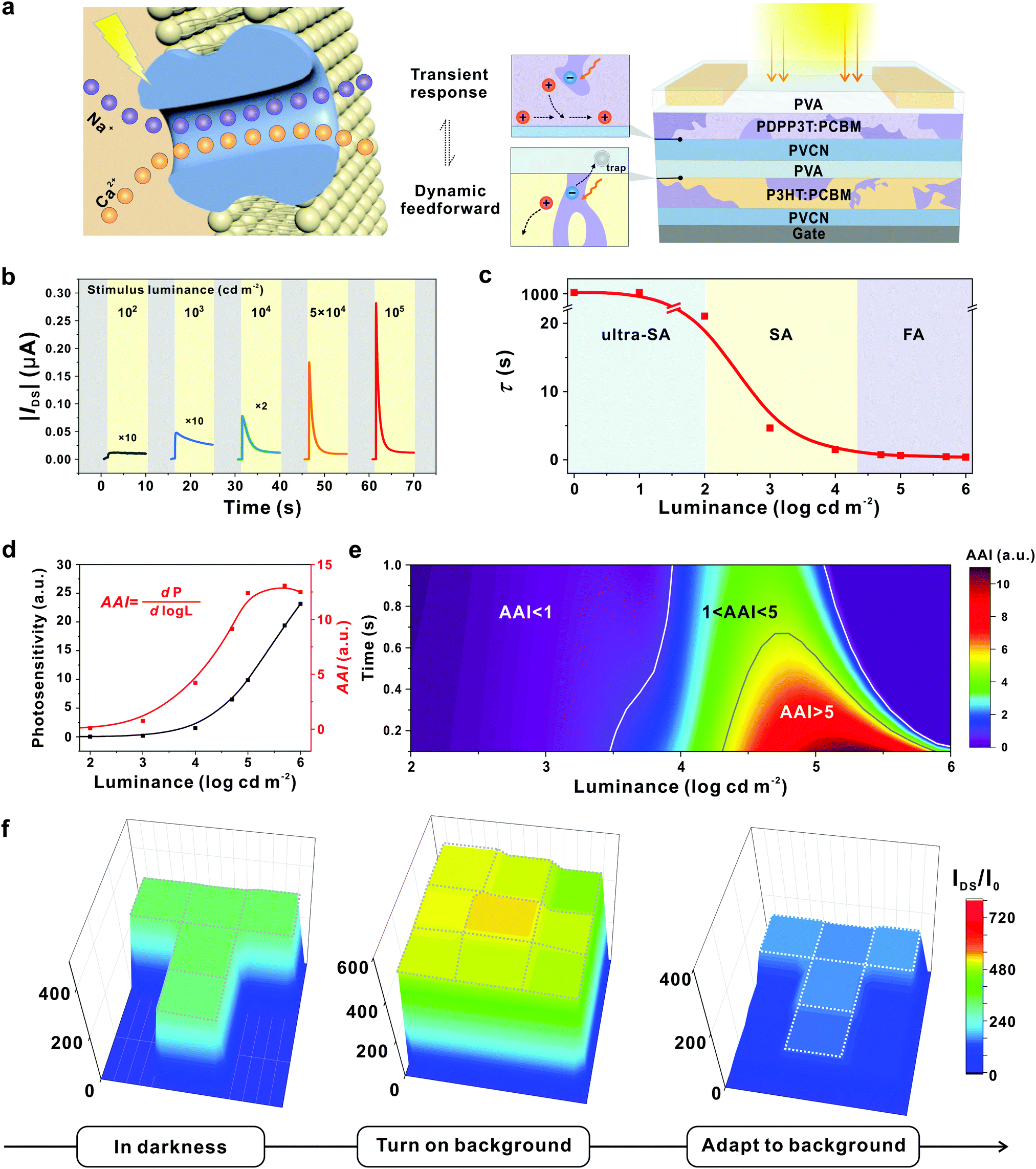 | ||
| Fig. 9 An organic transistor with light intensity-dependent active photoadaptation. (a) An organic phototransistor with two complementary bulk-heterojunctions inspired by the visual adaptation in human visual systems. (b) Real-time photoresponse of the device to various stimulus luminance. (c) Correlation between decay constant and luminance. The device can be modulated from ultra-SA, to SA and FA models according to the light intensities. (d) Correlation between photosensitivity (P) and AAI extracted at 0.1 s with varied luminance. Photosensitivity increases along with light stimuli; herein, the active adaptation index (AAI) is defined as the photosensitivity change as a function of orders of luminance magnitude (dP/dlogL), which reflects the adaption ability with varying light stimuli. (e) A time and luminance schematic diagram of the predicted tendency of AAI. (f) Resulting current mapping of the OAAT array under different conditions. With constant stimulus light intensity, the “T”-shaped image contrast decreases upon a bright-light background (104 cd m−2) and gradually shows the spatially resolved discrimination enabled by active adaptation. Reproduced with permission.44 Copyright 2021, Springer Nature. | ||
Output signals under various luminance stimuli exhibit fine-tuned transient photoresponse and dynamic adaptation in an automatic manner, and such a device can be classified into three distinctive models: from an ultraslow-adaptation (τ > 100 s) to slow- (1 < τ < 100 s) and fast-adaptation (τ < 1 s) (Fig. 9b and c). Upon light irradiation, photovoltaic effect-induced photoexcitation occurs in BHJs to produce a transient detector response, while the accumulation of trapped carriers in the dielectric layer contributes to the photo-triggered dynamic decay of the gating field. The coupling of the photovoltaic effect in two BHJs and dynamic electron trapping in the dielectric layer allows the adaptive modulation of carrier concentration in the conductive channel, leading to active photoadaptation behaviours in a single element.
To evaluate the performance of the OAAT, we defined AAI as a photosensitivity change along with the orders of luminance magnitude (Fig. 9d). The value remains less than 1 when the luminance stimulus is below 100 cd m−2; an enhanced luminance to 105 cd m−2 leads to notably increased AAI to 12.4. This tendency combined with the simulation results is comparable with the quasiquantitative value extracted from human visual systems,88 suggesting the successful realization of bionic visual adaptation with the fabricated device (Fig. 9d and e). In addition, this smart device exhibits active photoadaptation behaviors including dynamic adaptative response to continuous stimuli, decay-to-recovery features and superior background-dependent discrimination (less than 2s at 1 × 10⁴cd m−2) (Fig. 9f), suggesting that OAATs are promising systems to develop state-of-the-art active adaptation components.
4.5. Allowing diverse tactile adaptation by incorporating mechanical transduction
Certain adaptation applications require special types of devices with different development goals. For example, devices used to cope with dynamic force with high frequency demand FA elements, because in such conditions, a device needs to generate instantaneous electric signals only at the beginning and ending moments of stimulation, while SA elements are needed in response to static touch or pressure. To meet the requirement, devices that can imitate both SA and FA functions are in high demand. Transducers for mimicking SA typically rely on capacitive and piezoresistive effects as they can respond to static mechanical stimuli through continuous sensing signals (Fig. 10a).89,90 The capacitance (C) of a parallel plate capacitor is given by the equation C = εrε0A/d, where ε0 is the electric constant, εr is the relative permittivity, A is the area of overlap of the two plates, and d is the distance between the electrodes. A and D are easily changed by applying pressure, and thus cause the plate to deflect and the capacitance to change. Piezoresistive sensors transduce a change in the resistance of a device into an electrical signal. And, the change in contact resistance (Rc) between two materials created by the applied force (F) is the main source of the electrical signal change. Different from capacitive and resistive sensors, piezoelectric and triboelectric sensors can generate instantaneous electric signals under dynamic force stimuli, demonstrating capabilities similar to those of FA mechanoreceptors (Fig. 10b).91,92 Piezoelectricity refers to electrical charges generated in certain types of solid materials in response to an applied force, and the occurrence of electric dipole moments in solids contributes to the piezoelectric effect. The triboelectric effect is another commonly used transduction method only responding to dynamic stimuli, which is very suitable for mimicking FA.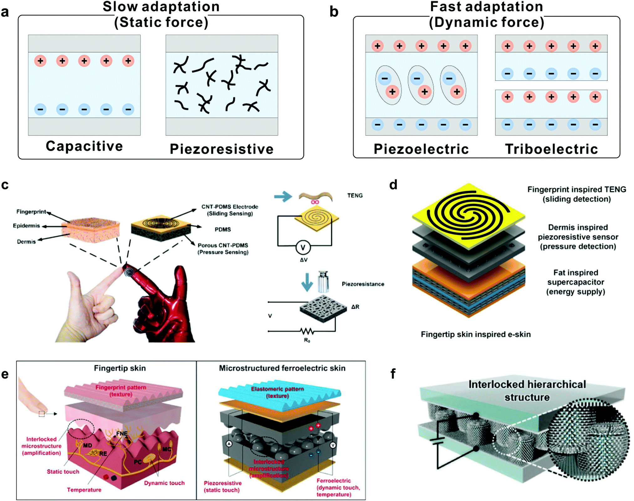 | ||
| Fig. 10 Construction of SA and FA devices through the piezoelectric effect. (a) Transduction mechanisms of capacitive and piezoresistive for mimicking slow adaptation mechanoreceptors. (b) Transduction mechanisms of piezoelectric and triboelectric for mimicking fast adaptation mechanoreceptors. (c) Fingertip-inspired e-skin based on triboelectric sliding sensing, and piezoresistive pressure detection. Reproduced with permission.38 Copyright 2017, Elsevier Ltd. (d) Schematic illustration of finger skin-inspired device. The device consists of a supercapacitor for energy supply, a piezoresistive sensor for pressure detection and a triboelectric generator for sliding detection. Reproduced with permission.40 Copyright 2018, Elsevier Ltd. (e) A skin-inspired microstructured ferroelectric device with interlocked geometry. Reproduced with permission.37 Copyright 2015, The Authors. (f) Schematic illustration of the e-skin device based on the interlocked hierarchical structure of ZnO NW arrays. Reproduced with permission.93 Copyright 2015, Wiley-VCH. | ||
Inspired by the perception functionalities of mechanoreceptors, a fingertip-like e-skin has been developed to discriminate FA and SA events (Fig. 10c).38 The device is based on a vertical structure composed of a sliding and pressure sensing part to enable the capabilities of FA and SA mechanoreceptors. In a similar way, a hybrid porous microstructure (HPMS) e-skin composed of a triboelectric generator and an HPMS pressure sensor was demonstrated to mimic FA and SA behaviors simultaneously (Fig. 10d).40 The structure of intermediate ridges also inspired studies to simulate different adaptation characteristics of mechanoreceptors. Ko et al. reported a multimodal e-skin based on the interlocked microdome structure by using ferroelectric polymer composites composed of PVDF and reduced graphene oxide (rGO) (Fig. 10e).37 In this device, the sustained static pressure can be detected by using the contact resistance change between the interlocked microdomes, while dynamic pressure detection can be achieved by using the piezoelectric sensing mode. Similarly, Ko and co-workers developed a pressure-sensitive e-skin in an interlocked geometry with a hierarchical ZnO nanowire (NW) array (Fig. 10f),93 and the device exhibited fine-tuned adaptation behavior according to the intensity or frequency of force stimuli. By exploiting various transduction methods, such devices can serve as powerful tools to adapt to various force stimuli.
5. Conclusions and perspectives
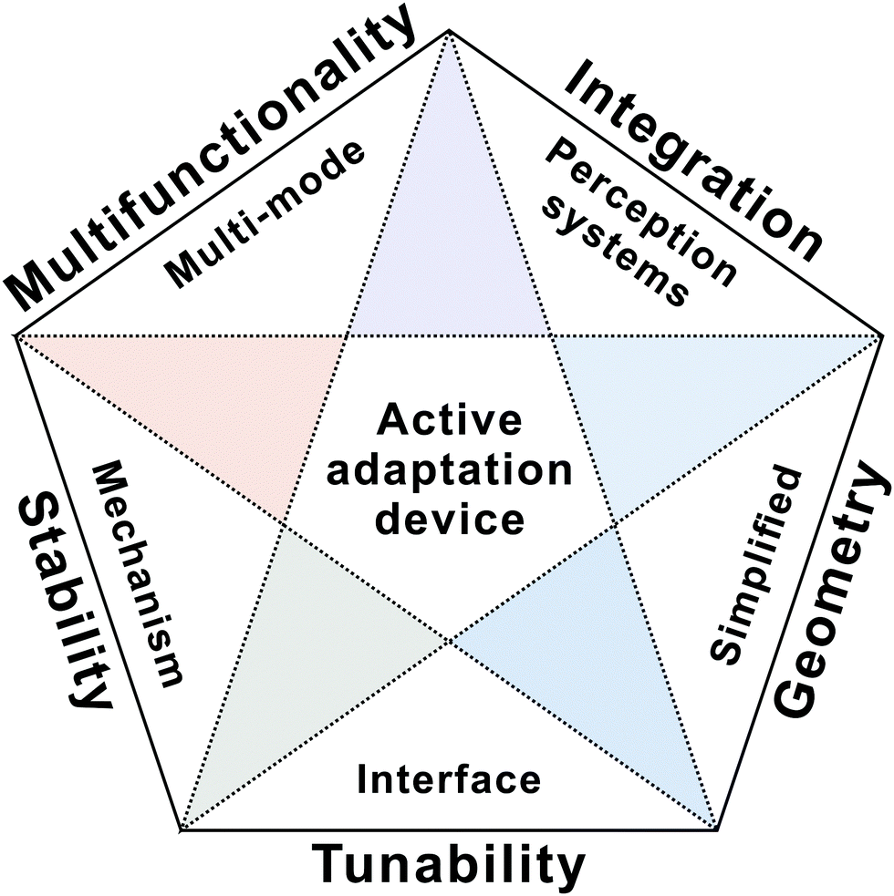
Adaptive devices aim to adjust their behaviour actively to varying stimuli. Several progressive studies have been made both in materials and device engineering. In spite of these achievements, many challenges lie ahead. What is the most efficient way to manipulate charge transport in a dynamic manner and realize diverse active adaptation? How to realize an excellent match in signal output between adaptive devices and biological organisms? Can we integrate adaptive devices with sensing and synaptic elements to create novel perception systems? To address these open questions, tremendous efforts should be made in the next five years.Human beings possess multi-mode adapting ability to various stimuli. For example, the human skin contains numerous mechanoreceptors and thermoreceptors to adapt to pressure stimuli and temperature change. However, the reported adaptive devices are currently in the primary stage of mimicking adaptation behaviours individually. More efforts will be devoted to developing multi-mode sensory adaptation mechanisms (Fig. 11). So far, recreating sensory adaptation in solid-state devices mainly relies on tactile- and visual-adaptation devices. Further investigation on the physiological processes of human beings in order to mimic full adaptation functionalities is also urgently needed in the future. In addition, device integration will attract increasing research interest in demonstrating fascinating features of adaptive systems. On the one hand, device-to-device variability remains a key issue, leading to obstacles in constructing large area device arrays with high densities and good uniformity. On the other hand, adaptive devices should be integrated with sensors or other neuromorphic devices to enable the next-generation artificial perception systems.
 | ||
| Fig. 11 The key aspects of adaptive devices that need to be focused on. | ||
Ideally, an adaptive element should be based on a single device, in order to pursue the simplest geometry and minimized power consumption. This dreaming task is difficult to achieve not only because of the paradoxical requirements of signal excitation and inhibition in one device, but also it relies on the existence of different stimuli. An initial attempt has been made by creating an OAAT to endow a transistor with photoadaptation functionality.44 Currently, this concept cannot be utilized to build other categories of active adaptation devices. Given that numerous sensing materials and device geometries have been developed, their incorporation with controlled manipulation of charge trapping will accelerate the development of active adaptation devices in an unexpected way.
Fine-tuning sensitivity and decay speed play an essential role in developing state-of-the-art adaptive devices in accordance with the needs of environmental conditions. So far, the limited understanding of biological adaptation and adaptive devices impedes the realization of well-modulated adaptation performance. In-depth investigation regarding the relationship of energy levels of active materials and charge transport/trapping at interfaces should be paid more attention. More materials should be developed to meet the requirements of various application conditions. Stability is another concern of adaptation devices. Existing adaptive devices focus on the manipulation of electrical behaviour in one cycle, leaving the improvement of long-term stability an open issue.
In conclusion, the adaptation device is essential for artificial perception systems, but there is a long way to go to make adaptive devices possessing comparable adaptation ability to that of human beings. Further development should focus on materials and device engineering to achieve balanced modulation of charge transport and trapping. By resolving these challenges, we expect a bright future of adaptive devices towards a new smart world.
Conflicts of interest
The authors declare no competing interests.Acknowledgements
We acknowledge financial support from the National Key Research and Development Program of China (2018YF-E0200700), the National Natural Science Foundation (62075224, 62001454, 22021002), the China Postdoctoral Science Foundation (2019M660798), the China National Postdoctoral Program for Innovative Talents (BX20190334), the K.C. Wong Education Foundation (GJTD-2020-02) and the Strategic Priority Research Program of Chinese Academy of Sciences (XDPB13).Notes and references
- M. Wang, Y. Luo, T. Wang, C. Wan, L. Pan, S. Pan, K. He, A. Neo and X. Chen, Adv. Mater., 2021, 33, 2003014 CrossRef CAS.
- X. Ji, X. Zhao, M. C. Tan and R. Zhao, Adv. Intell. Syst., 2020, 2, 1900118 CrossRef.
- J. Tang, F. Yuan, X. Shen, Z. Wang, M. Rao, Y. He, Y. Sun, X. Li, W. Zhang, Y. Li, B. Gao, H. Qian, G. Bi, S. Song, J. J. Yang and H. Wu, Adv. Mater., 2019, 31, 1902761 CrossRef CAS.
- M. L. Hammock, O. Knopfmacher, B. D. Naab, J. B.-H. Tok and Z. Bao, ACS Nano, 2013, 7, 3970–3980 CrossRef CAS.
- H. Shen, Y. Zou, Y. Zang, D. Huang, W. Jin, C.-A. Di and D. Zhu, Mater. Horiz., 2018, 5, 240–247 RSC.
- Z. Song, Y. Tong, X. Zhao, H. Ren, Q. Tang and Y. Liu, Mater. Horiz., 2019, 6, 717–726 RSC.
- D. Ye, J. Wang, H. Shen, X. Feng, L. Xiang, W. Jin, W. Zhao, J. Ding, Z. He, Y. Zou, Q. Meng, W. Cui, F. Zhang, C. A. Di, C. Fan and D. Zhu, Adv. Mater., 2021, 33, 2100489 CrossRef CAS.
- C. Qian, Y. Choi, Y. J. Choi, S. Kim, Y. Y. Choi, D. G. Roe, M. S. Kang, J. Sun and J. H. Cho, Adv. Mater., 2020, 32, 2002653 CrossRef CAS.
- B. Yang, Y. Lu, D. Jiang, Z. Li, Y. Zeng, S. Zhang, Y. Ye, Z. Liu, Q. Ou, Y. Wang, S. Dai, Y. Yi and J. Huang, Adv. Mater., 2020, 32, 2001227 CrossRef CAS.
- P. Gkoupidenis, D. A. Koutsouras and G. G. Malliaras, Nat. Commun., 2017, 8, 15448 CrossRef CAS.
- Y. van de Burgt, E. Lubberman, E. J. Fuller, S. T. Keene, G. C. Faria, S. Agarwal, M. J. Marinella, A. Alec Talin and A. Salleo, Nat. Mater., 2017, 16, 414–418 CrossRef CAS.
- C. Wu, T. W. Kim, H. Y. Choi, D. B. Strukov and J. J. Yang, Nat. Commun., 2017, 8, 752 CrossRef.
- H. R. Lee, D. Lee and J. H. Oh, Adv. Mater., 2021, 33, 2100119 CrossRef CAS.
- Y. R. Lee, T. Q. Trung, B. U. Hwang and N. E. Lee, Nat. Commun., 2020, 11, 2753 CrossRef CAS.
- H. Han, H. Yu, H. Wei, J. Gong and W. Xu, Small, 2019, 15, 1900695 CrossRef.
- Y. Lee and T. W. Lee, Acc. Chem. Res., 2019, 52, 964–974 CrossRef CAS.
- W. Xu, S. Y. Min, H. Hwang and T. W. Lee, Sci. Adv., 2016, 2, e1501326 CrossRef.
- Y. Zang, H. Shen, D. Huang, C. A. Di and D. Zhu, Adv. Mater., 2017, 29, 1606088 CrossRef.
- X. Pan, T. Jin, J. Gao, C. Han, Y. Shi and W. Chen, Small, 2020, 16, 2001504 CrossRef CAS.
- S. T. Keene, C. Lubrano, S. Kazemzadeh, A. Melianas, Y. Tuchman, G. Polino, P. Scognamiglio, L. Cinà, A. Salleo, Y. van de Burgt and F. Santoro, Nat. Mater., 2020, 19, 969–973 CrossRef CAS.
- Y. Tu and W. J. Rappel, Annu. Rev. Condens. Matter Phys., 2018, 9, 183–205 CrossRef.
- M. A. Webster, Annu. Rev. Vis. Sci., 2015, 1, 547–567 CrossRef.
- B. Wark, B. N. Lundstrom and A. Fairhall, Curr. Opin. Neurobiol., 2007, 17, 423–429 CrossRef CAS.
- Y. H. Jung, B. Park, J. U. Kim and T. I. Kim, Adv. Mater., 2019, 31, 1803637 CrossRef.
- F. A. Dunn, M. J. Lankheet and F. Rieke, Nature, 2007, 449, 603–606 CrossRef CAS.
- S. Seo, S. H. Jo, S. Kim, J. Shim, S. Oh, J. H. Kim, K. Heo, J. W. Choi, C. Choi, S. Oh, D. Kuzum, H. P. Wong and J. H. Park, Nat. Commun., 2018, 9, 5106 CrossRef.
- I. You, D. G. Mackanic, N. Matsuhisa, J. Kang, J. Kwon, L. Beker, J. Mun, W. Suh, T. Y. Kim, J. B.-H. Tok, Z. Bao and U. Jeong, Science, 2020, 370, 961–965 CrossRef CAS.
- L. Gu, S. Poddar, Y. Lin, Z. Long, D. Zhang, Q. Zhang, L. Shu, X. Qiu, M. Kam, A. Javey and Z. Fan, Nature, 2020, 581, 278–282 CrossRef CAS.
- R. A. John, N. Tiwari, M. I. B. Patdillah, M. R. Kulkarni, N. Tiwari, J. Basu, S. K. Bose, A. Ankit, C. J. Yu, A. Nirmal, S. K. Vishwanath, C. Bartolozzi, A. Basu and N. Mathews, Nat. Commun., 2020, 11, 4030 CrossRef CAS.
- H. Shen, Z. He, W. Jin, L. Xiang, W. Zhao, C. A. Di and D. Zhu, Adv. Mater., 2019, 31, 1905018 CrossRef CAS.
- S. M. Kwon, S. W. Cho, M. Kim, J. S. Heo, Y. H. Kim and S. K. Park, Adv. Mater., 2019, 31, 1906433 CrossRef CAS.
- S. Hong, S. H. Choi, J. Park, H. Yoo, J. Y. Oh, E. Hwang, D. H. Yoon and S. Kim, ACS Nano, 2020, 14, 9796–9806 CrossRef CAS.
- M. A. Misha, Proc. SPIE, 1991, 1473, 52–58 CrossRef.
- S.-C. Liu, Analog Integr. Circuits Process., 1999, 18, 243 CrossRef.
- C. Wang, H. Dong, W. Hu, Y. Liu and D. Zhu, Chem. Rev., 2012, 112, 2208–2267 CrossRef CAS.
- P. Gkoupidenis, N. Schaefer, B. Garlan and G. G. Malliaras, Adv. Mater., 2015, 27, 7176–7180 CrossRef CAS.
- J. Park, M. Kim, Y. Lee, H. S. Lee and H. Ko, Sci. Adv., 2015, 1, e1500661 CrossRef.
- H. Chen, L. Miao, Z. Su, Y. Song, M. Han, X. Chen, X. Cheng, D. Chen and H. Zhang, Nano Energy, 2017, 40, 65–72 CrossRef CAS.
- A. Chortos, J. Liu and Z. Bao, Nat. Mater., 2016, 15, 937–950 CrossRef CAS.
- H. Chen, Y. Song, H. Guo, L. Miao, X. Chen, Z. Su and H. Zhang, Nano Energy, 2018, 51, 496–503 CrossRef CAS.
- K. Y. Chun, Y. J. Son, E. S. Jeon, S. Lee and C. S. Han, Adv. Mater., 2018, 30, 1706299 CrossRef.
- H. Yuan, T. Lei, Y. Qin and R. Yang, Nano Energy, 2019, 59, 84–90 CrossRef CAS.
- X. Wu, J. Zhu, J. W. Evans and A. C. Arias, Adv. Mater., 2020, 32, 2005970 CrossRef CAS.
- Z. He, H. Shen, D. Ye, L. Xiang, W. Zhao, J. Ding, F. Zhang, C. A. Di and D. Zhu, Nat. Electron., 2021, 4, 522–529 CrossRef CAS.
- K.-C. Lee, S.-Y. Huang, M.-Y. Tsai, S.-H. Yang, C.-Y. Lin, M. Li, Y.-M. Chang, K. Watanabe, T. Taniguchi, Y.-C. Lai, S.-P. Lin, P.-W. Chiu and Y.-F. Lin, Matter, 2021, 4, 1598–1610 CrossRef CAS.
- D. Xie, L. Wei, M. Xie, L. Jiang, J. Yang, J. He and J. Jiang, Adv. Funct. Mater., 2021, 31, 2010655 CrossRef CAS.
- S. Chun, J.-S. Kim, Y. Yoo, Y. Choi, S. J. Jung, D. Jang, G. Lee, K.-I. Song, K. S. Nam, I. Youn, D. Son, C. Pang, Y. Jeong, H. Jung, Y.-J. Kim, B.-D. Choi, J. Kim, S.-P. Kim, W. Park and S. Park, Nat. Electron., 2021, 4, 429–438 CrossRef.
- W. W. Lee, Y. J. Tan, H. Yao, S. Li, H. H. See, M. Hon, K. A. Ng, B. Xiong, J. S. Ho and B. C. K. Tee, Sci. Robot., 2019, 4, eaax2198 CrossRef.
- A. Nikolaev, K. M. Leung, B. Odermatt and L. Lagnado, Nat. Neurosci., 2013, 16, 934–941 CrossRef CAS.
- M. Mendelson and W. R. Loewenstein, Science, 1964, 144, 554–555 CrossRef CAS.
- R. S. Johansson and J. R. Flanagan, Nat. Rev. Neurosci., 2009, 10, 345–359 CrossRef CAS.
- S. M. Smirnakis, M. J. Berry, D. K. Warland, W. Bialek and M. Meister, Nature, 1997, 386, 69–73 CrossRef CAS.
- V. Mante, R. A. Frazor, V. Bonin, W. S. Geisler and M. Carandini, Nat. Neurosci., 2005, 8, 1690–1697 CrossRef CAS.
- A. B. Artyukhin, L. F. Wu and S. J. Altschuler, Cell, 2009, 138, 619–621 CrossRef CAS.
- S. M. Smirnakis, M. J. Berry, D. K. Warland, W. Bialek and M. Meister, Nature, 1997, 386, 69–73 CrossRef CAS.
- A. Tendler, B. C. Wolf, V. Tiwari, U. Alon and A. Danon, iScience, 2018, 8, 126–137 CrossRef CAS.
- W. Ma, A. Trusina, H. El-Samad, W. A. Lim and C. Tang, Cell, 2009, 138, 760–773 CrossRef CAS.
- P. Delmas, J. Hao and L. Rodat-Despoix, Nat. Rev. Neurosci., 2011, 12, 139–153 CrossRef CAS.
- B. Wark, A. Fairhall and F. Rieke, Neuron, 2009, 61, 750–761 CrossRef CAS.
- F. Yavari, M. Amiri, F. N. Rahatabad, E. Falotico and C. Laschi, Neurocomputing, 2020, 379, 343–355 CrossRef.
- B. C.-K. Tee, A. Chortos, A. Berndt, A. K. Nguyen, A. Tom, A. McGuire, Z. C. Lin, K. Tien, W.-G. Bae, H. Wang, P. Mei, H.-H. Chou, B. Cui, K. Deisseroth, T. N. Ng and Z. Bao, Science, 2015, 350, 313–316 CrossRef CAS.
- Y. Kim, A. Chortos, W. Xu, Y. Liu, J. Y. Oh, D. Son, J. Kang, A. M. Foudeh, C. Zhu, Y. Lee, S. Niu, J. Liu, R. Pfattner, Z. Bao and T. W. Lee, Science, 2018, 360, 998–1003 CrossRef CAS.
- S. Chun, I. Hwang, W. Son, J. H. Chang and W. Park, Nanoscale, 2018, 10, 10545–10553 RSC.
- S. Chun, A. Hong, Y. Choi, C. Ha and W. Park, Nanoscale, 2016, 8, 9185–9192 RSC.
- L. D. Rosenblum, See what I'm saying: The extraordinary powers of our five senses, WW Norton & Company, 2011.
- S. M. Smirnakis, M. J. Berry, D. K. Warland, W. Bialek and M. Meister, Nature, 1997, 386, 69–73 CrossRef CAS.
- A. Stockman and L. T. Sharpe, Ophthal. Physiol. Opt., 2006, 26, 225–239 CrossRef.
- D. Dev, A. Krishnaprasad, H. Kalita, S. Das, V. Rodriguez, J. Calderon Flores, L. Zhai and T. Roy, Appl. Phys. Lett., 2018, 112, 232101 CrossRef.
- J. Jiang, J. Guo, X. Wan, Y. Yang, H. Xie, D. Niu, J. Yang, J. He, Y. Gao and Q. Wan, Small, 2017, 13, 1700933 CrossRef.
- D. Jariwala, V. K. Sangwan, L. J. Lauhon, T. J. Marks and M. C. Hersam, ACS Nano, 2014, 8, 1102–1120 CrossRef CAS.
- D. E. Koshland, A. Goldbeter and J. B. Stock, Science, 1982, 220–225 CrossRef CAS.
- Y. Cheng, H. Li, B. Liu, L. Jiang, M. Liu, H. Huang, J. Yang, J. He and J. Jiang, Small, 2020, 16, 2005217 CrossRef CAS.
- Y. Cheng, K. Shan, Y. Xu, J. Yang, J. He and J. Jiang, Nanoscale, 2020, 12, 21798–21811 RSC.
- H. L. Park, H. Kim, D. Lim, H. Zhou, Y. H. Kim, Y. Lee, S. Park and T. W. Lee, Adv. Mater., 2020, 32, 1906899 CrossRef CAS.
- H. Shen, C.-A. Di and D. Zhu, Sci. China: Chem., 2017, 60, 437–449 CrossRef CAS.
- W. Shi, Y. Guo and Y. Liu, Adv. Mater., 2020, 32, e1901493 CrossRef.
- S. Dai, X. Wu, D. Liu, Y. Chu, K. Wang, B. Yang and J. Huang, ACS Appl. Mater. Interfaces, 2018, 10, 21472–21480 CrossRef CAS.
- D. I. Kim, T. Q. Trung, B. U. Hwang, J. S. Kim, S. Jeon, J. Bae, J. J. Park and N. E. Lee, Sci. Rep., 2015, 5, 12705 CrossRef CAS.
- J. Hao and P. Delmas, J. Neurosci., 2010, 30, 13384–13395 CrossRef CAS.
- N. Gupta and M. Stopfer, Curr. Opin. Neurobiol., 2011, 21, 768–773 CrossRef CAS.
- C. Wang, X. Zhang and W. Hu, Chem. Soc. Rev., 2020, 49, 653–670 RSC.
- D. Ji, T. Li, J. Liu, S. Amirjalayer, M. Zhong, Z.-Y. Zhang, X. Huang, Z. Wei, H. Dong, W. Hu and H. Fuchs, Nat. Commun., 2019, 10, 12 CrossRef CAS.
- I. Zliobaite and B. Gabrys, IEEE Trans. Knowl. Data Eng., 2012, 26, 309–321 Search PubMed.
- Y. Koutalos and K.-W. Yau, Trends Neurosci., 1999, 19, 73–81 CrossRef.
- D. Baylor, Proc. Natl. Acad. Sci. U. S. A., 1996, 93, 560–565 CrossRef CAS.
- V. Torre, J. F. Ashmore, T. D. Lamb and A. Menini, J. Neurosci., 1995, 15, 7757–7768 CrossRef CAS.
- P. A. Iglesias, Sci. Signaling, 2012, 5, pe8 CrossRef.
- J. C. Stevens and S. S. Stevens, J. Opt. Soc. Am., 1963, 53, 375–385 CrossRef CAS.
- J.-W. Han, B. Kim, J. Li and M. Meyyappan, Appl. Phys. Lett., 2013, 102, 051903 CrossRef.
- H. Chen, Z. Su, Y. Song, X. Cheng, X. Chen, B. Meng, Z. Song, D. Chen and H. Zhang, Adv. Funct. Mater., 2017, 27, 1604434 CrossRef.
- S. Wang, L. Lin and Z. L. Wang, Nano Energy, 2015, 11, 436–462 CrossRef CAS.
- L. Lin, Y. Xie, S. Wang, W. Wu, S. Niu, X. Wen and Z. L. Wang, ACS Nano, 2013, 7, 8266–8274 CrossRef CAS.
- M. Ha, S. Lim, J. Park, D.-S. Um, Y. Lee and H. Ko, Adv. Funct. Mater., 2015, 25, 2841–2849 CrossRef CAS.
| This journal is © The Royal Society of Chemistry 2022 |