
Visible-blind ultraviolet narrowband photomultiplication-type organic photodetector with an ultrahigh external quantum efficiency of over 1![[thin space (1/6-em)]](https://www.rsc.org/images/entities/h2_char_2009.gif) 000000%†
000000%†
Dechao
Guo
 ab,
Liqing
Yang
a,
Jingcheng
Zhao
a,
Ji
Li
a,
Guo
He
a,
Dezhi
Yang
*a,
Linge
Wang
*b,
Agafonov
Vadim
c and
Dongge
Ma
*a
ab,
Liqing
Yang
a,
Jingcheng
Zhao
a,
Ji
Li
a,
Guo
He
a,
Dezhi
Yang
*a,
Linge
Wang
*b,
Agafonov
Vadim
c and
Dongge
Ma
*a
aCenter for Aggregation-Induced Emission, Institute of Polymer Optoelectronic Materials and Devices, Guangdong Provincial Key Laboratory of Luminescence from Molecular Aggregates, State Key Laboratory of Luminescent Materials and Devices, South China University of Technology, Guangzhou 510640, People's Republic of China. E-mail: msdgma@scut.edu.cn; msdzyang@scut.edu.cn
bSouth China Advanced Institute for Soft Matter Science and Technology, School of Molecular Science and Engineering, Guangdong Provincial Key Laboratory of Functional and Intelligent Hybrid Materials and Devices, South China University of Technology, Guangzhou 510640, China. E-mail: lingewang@scut.edu.cn
cMoscow Institute of Physics and Technology, Dolgoprudny, Moscow Region, 141700, Russia
First published on 17th June 2021
Abstract
A visible-blind ultraviolet (UV) photodetector can detect UV signals and is not interfered with by visible light or infrared light in the environment. In order to realize high-performance visible-blind UV organic photodetectors (OPDs), we design photomultiplication-type (PM-type) OPDs by using a novel strategy. Firstly, wide bandgap organic semiconductor materials, which do not absorb visible light, are selected as donors to absorb UV light. Secondly, a very small amount of C60 is used as an acceptor to trap photogenerated electrons. These accumulating electrons near the Al electrode form a potential, which leads to band bending and narrowing of the interface barrier, thereby assisting hole-tunneling injection to form a multiplication. The fabricated visible-blind UV PM-type OPDs with donor/acceptor doping ratio of 50![[thin space (1/6-em)]](https://www.rsc.org/images/entities/char_2009.gif) :1 exhibit a narrowband response with full-width at half-maximum (FWHM) of approximately 36 nm, an ultrahigh external quantum efficiency of 1.08 × 10⁶% and a remarkable specific detectivity of 1.28 × 10¹⁴ jones at 335 nm wavelength under −14 V bias. The UV-to-visible rejection ratio exceeds 103 by adjusting the donor/acceptor mixing ratios. The devices made with other wide bandgap organic materials also showed similar performance, indicating that this device structure provides an effective method for the preparation of high-performance visible-blind UV PM-type OPDs. In addition, we prepared a flexible visible-blind UV PM-type OPD based on a PET substrate and integrated it with a flexible OLED to fabricate a wearable UV monitor, which can visually detect the intensity of UV light.
:1 exhibit a narrowband response with full-width at half-maximum (FWHM) of approximately 36 nm, an ultrahigh external quantum efficiency of 1.08 × 10⁶% and a remarkable specific detectivity of 1.28 × 10¹⁴ jones at 335 nm wavelength under −14 V bias. The UV-to-visible rejection ratio exceeds 103 by adjusting the donor/acceptor mixing ratios. The devices made with other wide bandgap organic materials also showed similar performance, indicating that this device structure provides an effective method for the preparation of high-performance visible-blind UV PM-type OPDs. In addition, we prepared a flexible visible-blind UV PM-type OPD based on a PET substrate and integrated it with a flexible OLED to fabricate a wearable UV monitor, which can visually detect the intensity of UV light.
New conceptsThe novel concept of preparing visible-blind narrowband UV PM-type OPDs by selecting wide bandgap organic semiconductor materials as the donor and a very small amount of C60 as the acceptor has been demonstrated. The absorption of visible light by the active material can be effectively weakened, which is very beneficial for the device to achieve UV visible-blind characteristics. Ultra-high EQE values are also achieved by the photomultiplication process due to the unbalanced charge transport properties induced by the low-doping system. Also, the approximate performances were obtained using other wide bandgap materials, indicating that our preparation method exhibits universal applicability. In addition, unlike previous studies, we used the vacuum evaporation method to prepare the devices, avoiding the problems of easy aggregation of inorganic nanoparticles and poor reproducibility of device performance in conventional polymer/inorganic hybrid systems. Considering the high photomultiplication and UV-selective response characteristics of the prepared UV PM-type OPD, we integrated a flexible UV PM-type OPD with a flexible OLED to obtain a wearable UV monitor, which can detect weak UV light without an additional external current amplifier. Our research will provide a new idea for the preparation and application of visible-blind UV PM-type OPDs. |
Introduction
Photodetectors have a wide range of applications for imaging systems, artificial vision systems, environmental surveillance and remote monitoring.1–3 Organic photodetectors (OPDs) are becoming increasingly attractive due to the unique optical and electrical properties of organic semiconductors, such as lightweight, transparency, mechanical flexibility and adjustable absorption spectrum.4–6 Among OPDs, narrowband OPDs, which can effectively detect light signals of specific wavelengths, are especially useful in the fields of spectroscopy, fluorescence microscopy, environmental analysis, surveillance, and defense applications.7–9 To achieve the narrowband response, the most common method is developing materials with a narrow light absorption characteristic. Besides, combining a bandpass optical filter with photodetectors to detect light of various wavelengths is also an effective method. However, this approach not only limits the sensitivity and responsivity of OPDs due to the optical transmission delays and attenuations, but also complicates the design and increases the cost. The ideal narrowband OPDs should be able to detect the required spectrum without using bandpass optical filters. Recently, Burn's group10 proposed a new strategy to achieve narrowband response photodetectors via the charge collection narrowing (CCN) method. The mechanism of CCN is that light with different wavelengths has different charge collection efficiency because of its different penetration depth in the active layer. When the active layer thickness is increased from the nanometer range to the micrometer range, only long-wavelength light can penetrate through the entire active layer. Therefore, narrowband response characteristics can be achieved by increasing the thickness of the active layer. However, this method is suitable for the preparation of red or near-infrared (NIR) OPDs instead of UV OPDs. Combined with the CCN mechanism, Zhang et al.11 reported red-light narrowband response PM-type OPDs based on a thick P3HT:PC71BM (100:1, wt/wt) active layer by using trapped electron induced hole tunneling injection. The champion EQE value of the PM-type OPDs remarkably increased to 53500% under a high bias of −60 V. At the same time, the FWHM of about 30 nm was successfully achieved. Although the red-light response PM-type OPDs shows good narrowband response characteristics, the relatively high applied reverse bias needs to be further reduced to meet requirements for practical applications.
UV-PDs have a wide range of applications, such as chemical, environmental and biological analyses and monitoring, flame and radiation detection, astronomical studies, missile detection and optical communications.12–14 UV PM-type OPDs have been reported by using organic–inorganic blending active layers, where the inorganic nanoparticles (such as ZnO and TiO2) served as electron traps to enhance hole injection from the cathode. Huang et al.15 reported UV PM-type OPDs using ZnO nanoparticles combined with poly(vinyl carbazole) (PVK) as an active layer, which exhibited ultrahigh EQE peaks of up to 2.4 × 10⁵% and a peak specific detectivity (D*) of 3.4 × 10¹⁵ jones under a reverse bias of −9 V and 360 nm illumination. Then, they also reported narrowband PM-type organic/inorganic hybrid photodetectors by introducing CdTe16 and PbS17 quantum dots (QDs) as charge traps into the photoactive layer. These OPDs achieved PM characteristics by doping QDs and exhibited a narrowband response in red light and NIR due to the limitation of QDs absorbing long wavelengths. Shao et al.18 fabricated UV PM-type OPDs based on a nanocomposite active layer composed of TiO2 blended with 1,3-bis(Ncarbazolyl)benzene (mCP), which showed an EQE of about 8.5 × 10⁴% under a reverse bias of −10 V and 351 nm illumination. Yu et al.19 fabricated flexible UV PM-type OPDs on ITO-coated poly(ethylene terephthalate) substrates with a nanocomposite active layer composed of ZnO nanoparticles blended with a wide bandgap conjugated polymer, poly(9,9-dioctylfluorenyl-2,7-diyl)-alt-co-(bithiophene) (F8T2). The maximum EQE reached 2170% under 360 nm light illumination and 220% under 510 nm light illumination at −15 V bias, and both EQE peaks had FWHM values below 20 nm. Although the UV PM-type OPDs can be achieved by using organic–inorganic active layers, it is necessary to further improve the stability and repeatability since inorganic nanoparticles are prone to aggregation. Although the above-mentioned breakthroughs in EQE have been achieved, the devices have more or less response to visible light, which does not meet the requirements of visible-blind UV-PDs.
At present, there are no reports on visible-blind UV PM-type OPDs prepared with fully organic materials, mainly because most organic materials absorb visible light and lack an effective wide bandgap donor–acceptor material combination. Therefore, the preparation of high-performance visible-blind UV PM-type OPDs faces a great challenge. Here, we designed and successfully fabricated visible-blind UV narrowband PM-type OPDs using TAPC:C60 with a weight ratio of 50:1 as the active layer. The wide bandgap organic semiconductor material TAPC was used as a donor to achieve a visible-blind UV response. A very small amount of the acceptor C60 which weakens the visible light response was used as the trap center of electrons to achieve the PM. The fabricated UV PM-type OPD exhibited strong UV-selectivity with the FWHM about 36 nm and a spectral response cutoff around 370 nm with a UV/visible rejection ratio of about 620. The combination of a high PM mechanism with narrowband response characteristics makes the resulting OPDs highly efficient and selective for UV detection. The maximum EQE and D* values of the fabricated visible-blind UV PM-type OPDs reached 1.08 × 10⁶% and 1.28 × 10¹⁴ jones under 335 nm illumination at −14 V bias, respectively. Obviously, the utilization of the simple device structure in the fabricated visible-blind UV PM-type OPDs with ultra-high photoresponse greatly simplifies the preparation process and reduces the production cost, which has great prospects in the fields of large-area flexible devices.
Experimental section
Materials
The hole-injection material of di-[4-(N,N-ditolyl-amino)-phenyl]cyclohexane (HAT-CN), hole transporting materials of di-4-(N,N-di-p-tolyl-amino)-phenylcyclohexane (TAPC), N,N′-bis(naphthalen-1-yl)-N,N′-bis(phenyl)-benzidine (NPB), 4,4′-bis(carbazol-9-yl)biphenyl (CBP), 4,4′,4′′-tris(N-3-methylphenyl-N-phenyl-amino)triphenylamine (m-MTDATA) and 4,4′,4′′-tris(carbazol-9-yl)triphenylamine (TCTA), electron-transporting materials of fullerene-C60 (C60) and bis[2(2-hydroxyphenyl)pyridinato]beryllium (Bepp2), electron-injection material of 8-hydroxyquinolatolithium (Liq), and green phosphorescent material of bis(2phenylpyridine)iridium(III)-acetylacetonate [Ir(ppy)2(acac)] were purchased from Jilin OLED Material Tech Co. Ltd. All the materials were used as received.Fabrication of PM-type OPDs
The substrates were first thoroughly cleaned using detergents and deionized water successively in an ultrasonic bath for 90 minutes. Then, the devices were fabricated by vacuum thermal evaporation of the organic materials on cleaned ITO-coated glass substrates with a sheet resistance of 10 Ω sq−1. TAPC and C60 active layer materials were simultaneously evaporated under high vacuum conditions (pressure ∼10−5 Pa) to obtain a blend film. The aluminum (Al) electrodes were deposited on the active layer through a shadow mask. The thickness of the active layer and Al electrode was controlled in situ by a quartz crystal monitor and calibrated by a D-150 surface profiler (Veeco Precision Instrument Co., Ltd). The active area of each device was 16 mm2.Characterization of PM-type OPDs
The UV-Vis absorption spectrum of the organic materials on a quartz substrate was measured using a Hitachi U-4100 spectrophotometer. The EQE of the PM-type OPDs was measured by using a phase-locking technique. The incident light from a halogen lamp (250 W) was modulated at 4 Hz by a chopper, then passed through a double monochromator and focused on the active areas of the devices. The photocurrent signal generated by the PM-type OPDs was first amplified by a low-noise transimpedance amplifier (SR570, Stanford Research Systems), and then detected using the SR830 lock-in amplifier. The reverse biases on the PM-type OPDs were provided by Keithley 236 sourcemeters. A crystalline silicon photodiode (S1337-1010BQ, Hamamatsu) calibrated by the National Institute of Metrology of China was used as a reference before each measurement. For the dark current measurement, the current–voltage characteristics were recorded using a Keithley 2636B source measurement unit. In order to avoid interference from external noise signals, the PM-type OPDs were shielded in a metal case for testing. All the measurements were carried out under ambient conditions.Results and discussion
The device structure and the molecular structures of the used active materials are shown in Fig. 1. ITO and Al are used as the anode and cathode of the devices, respectively, and the TAPC:C60 blend film is used as the photoactive layer of the devices. The wide bandgap of TAPC as a donor can ensure that it has strong UV absorption and almost no absorption in the visible light region. In addition, its hole mobility as high as 1 × 10⁻² cm2 V−1 s−120 can also help improve the device performance. C60 is a commonly used electron acceptor material in organic photovoltaics due to its high electron mobility of 1.6 cm2 V−1 s−1.21 Moreover, C60 is a good electron transport material with a much longer hole trapping time than electron transit time.22 Thus, C60 with a low doping ratio will form isolated “clusters” in the active layer, which will make it difficult to form a continuous electron transport channel in devices. Therefore, C60 is used as both the acceptor material and the carrier trapping defect to realize the PM process. The energy band diagram of the fabricated visible-blind UV PM-type OPDs is shown in Fig. 1c. TAPC possesses a very large HOMO value, which leads to a large hole injection barrier between the HUMO of TAPC and the work function of Al. As a result, the hole injection from the Al electrode to TAPC is greatly suppressed, which is beneficial for reducing the dark current of the devices. The UV-vis absorption spectra of TAPC, C60 and TAPC:C60 blend thin films are presented in Fig. 1d. It can be seen that the absorption of TAPC is mainly in the UV region, and is weak in the visible light range with the absorption cut-off wavelength located at 370 nm, which corresponds to its wide optical bandgaps of 3.5 eV. The absorption range of C60 includes both UV and visible light ranges and is stronger in the UV region. The TAPC:C60 blend film with the doping ratio of 50:1 shows strong absorption between 300 and 370 nm with a peak around 335 nm, which is similar to the pure TAPC film. Due to the low weight ratio of C60, the absorption of the TAPC:C60 blend film only exhibits a slight increase in the visible light range, as shown in the inset of Fig. 1d, so the spectral response range of the devices will be mainly determined by the donor materials.
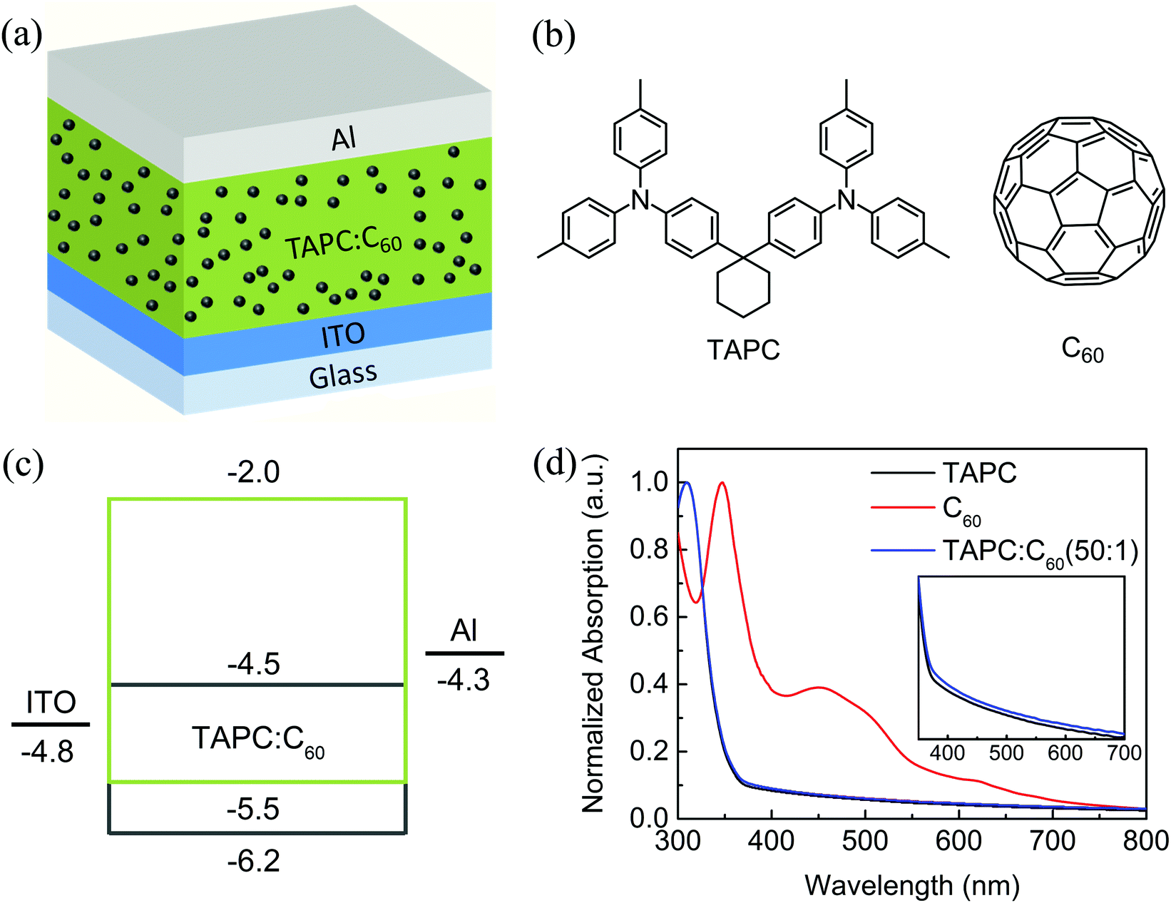 | ||
| Fig. 1 (a) Device structure diagram of the fabricated UV PM-type OPDs. (b) Chemical structures of the used organic materials. (c) Energy level diagram of the fabricated UV PM-type OPDs. (d) Normalized absorption spectra of TAPC, C60 and TAPC:C60 blend films. Inset: Absorption spectra of TAPC and TAPC:C60 (50:1, wt/wt) films in the wavelength range of 350–700 nm. | ||
EQE is defined as the ratio of charge carriers collected to incident photons, which can be calculated by applying the equation: EQE = (Jph/q)/(Pin/hν) = (JL − Jd)hν/qPin, where Jph is the photogenerated current density, q is the elementary charge (1.6 × 10⁻¹⁹ C), Pin is the incident light intensity, h is Planck's constant, ν is the spectral frequency, JL is photocurrent density, and Jd is dark current density. An EQE value exceeding 100% indicates that the devices have realized the PM process, namely, multiple charge carriers can be collected per incident photon. We characterized the EQE spectra of the fabricated UV PM-type OPDs under different reverse biases. As shown in Fig. 2a, the devices exhibit a narrowband response ranging from 300 nm to 370 nm, which agrees well with the absorption spectra of active layer materials. Meanwhile, the EQE values are dramatically increased with the increase of applied bias, which can be attributed to the enhancement of hole-tunneling injection and hole transport ability resulting from the increase of the internal electric field in the device. As we know, the energy level of TAPC will be more tilted under a larger applied bias, which can further decrease the width of the hole tunneling barrier from the Al cathode into the active layer, thereby enhancing the hole injection. In addition, the hole transport ability in the active layer is also accelerated under high voltage, which shortens the transport time of the holes for passing through the whole active layer. The peak EQE as high as 1.08 × 10⁶% at 335 nm wavelength under −14 V bias is achieved, which should be the maximum value in the reported PM-type OPDs. The peak EQE values of our device and the reported organic or organic/inorganic photodetectors are summarized in the inset of Fig. 2a.25–28,30–44 The ultrahigh gain characteristics of our PM-type OPDs can be attributed to the fact that the low doping C60 can effectively trap electrons and enhance hole tunneling injection. In addition, the injected holes can quickly transport to the anode through the HOMO level of TAPC due to its high hole mobility, reducing the recombination probability of holes and electrons. In order to verify the versatility and effectiveness of the device structure, we prepared the PM-type OPDs using several common wide bandgap organic hole transport materials (CBP, TCTA, m-MTDATA, and NPB) as a donor. The EQE characteristics of all the fabricated OPDs are shown in Fig. S1 (ESI†). It can be seen that all the devices have excellent PM effects, and the maximum EQE values reach 55413%, 208333%, 238817% and 347267%, respectively. Moreover, all the fabricated PM-type OPDs show good narrowband response characteristics with the FWHM of ∼34 nm, ∼33 nm, ∼62 nm and ∼74 nm, respectively. In addition, the EQE curve of the devices is consistent with the absorption spectrum shape of the respective hole transport material, as shown in Fig. S2 (ESI†). This further indicates that the method of reducing the acceptor doping ratio is an effective way to prepare narrowband response PM-type OPDs, and the spectral response range is mainly determined by the donor materials. On the other hand, the EQE values of the devices corresponding to these wide bandgap materials are lower than that of the TAPC-based device, which can be explained by the equation: EQE = χτ/T = χτμV/L2 (χ is the fraction of excitons that dissociate into charge carriers, τ is the lifetime of the trapped electrons, T is the hole transport time, μ is the hole mobility, V is the applied bias, and L is the thickness of the active layer).23,24 It is clear that EQE is proportional to the hole transport capacity of the active layer. As shown in Fig. S3 (ESI†), TAPC has the highest hole mobility, which leads to the corresponding devices exhibiting the highest EQE values. Moreover, since the hole injection barrier between the m-MTDATA and Al electrode is significantly smaller, the EQE values of the corresponding devices are instead lower despite the fact that TCTA and CBP have a relatively higher hole mobility than m-MTDATA. Therefore, the EQE values of PM-type OPDs are determined by a combination of the hole tunneling injection process and the hole transport capacity of the active layer.
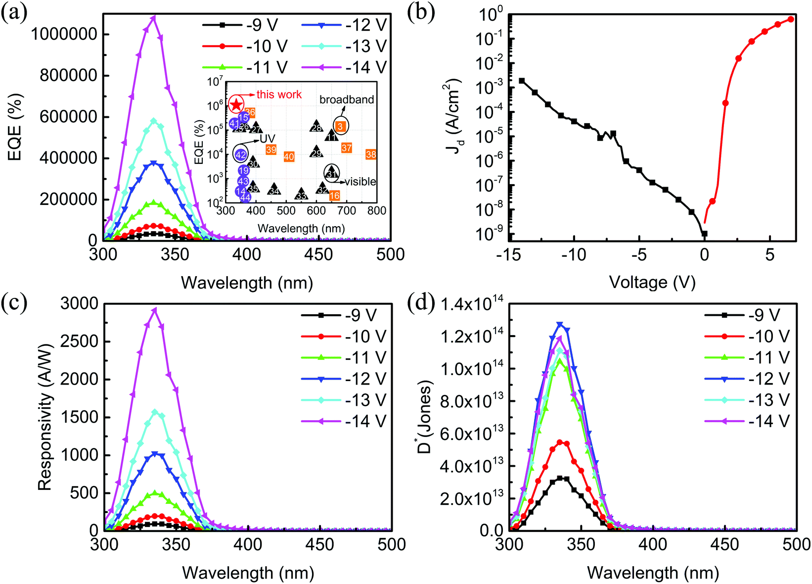 | ||
| Fig. 2 (a) EQE, (b) Jd − V, (c) R, and (d) D* characteristics of the fabricated UV PM-type OPDs under different applied voltages. The device structure is ITO/TAPC:C60(50:1, 80 nm)/Al(100 nm). Inset of (a): summary of the peak EQEs of our prepared devices and the reported organic or organic/inorganic photodetectors. | ||
The dark current density versus voltage (Jd − V) curve of the fabricated UV PM-type OPDs is shown in Fig. 2b. Under reverse bias conditions, electrons can be easily injected from ITO into the LUMO of C60 because of the relatively small electron injection barrier of about 0.3 eV. However, the electron current can be neglected because the doping ratio of C60 is too low to form a continuous electron transport channel in the active layer. Holes can be hardly injected from the Al cathode into the HOMO of TAPC because of the relatively large hole injection barrier of about 1.2 eV. Therefore, the fabricated UV PM-type OPDs exhibit a low Jd under reverse bias. Under forward bias conditions, the electrons cannot still be effectively transported in the active layer due to the absence of continuous electron transport channels. However, the holes can be injected from ITO into the HOMO of TAPC due to the relatively small hole injection barrier of about 0.7 eV, resulting in a larger dark current under forward bias conditions than that under the reverse biased conditions.
To further evaluate the device performance, the corresponding responsivity (R) and specific detectivity (D*) of the fabricated PM-type OPDs were calculated. The value of R is calculated according to the equation: R = EQE × hν/q, where hν is the energy of the incident photon in electron-volts, and q is the electron charge. The photoresponsivity spectra of the fabricated devices under different bias voltages are shown in Fig. 2c. Under −14 V reverse bias, the maximum R up to 2.91 × 10³ A W−1 is obtained at 335 nm wavelength. On the assumption that the total noise-current is dominated by a shot noise component in the dark current, D* can be expressed as D* = R/(2qJd)1/2, where q is the electron charge and Jd is the dark current density of the device. As shown in Fig. 2d, the D* value reaches a maximum value of 1.28 × 10¹⁴ jones at λ = 335 nm under the bias of −14 V, which is one of the largest values among those of the previously reported UV narrowband response PM-type OPDs.29 The high R and D* values of the fabricated PM-type OPDs should be attributed to the relatively large EQE and small dark current.
The working processes of our UV PM-type OPDs in the dark and light are shown in Fig. 3. Under dark and reverse bias conditions, the low concentration of C60 makes electrons difficult to transport to the Al electrode, and the large hole injection barrier also makes hole injection difficult. Therefore, the device exhibits low dark current characteristics. As illustrated in Fig. 3b, the TAPC:C60 active layer absorbs incident photons and generates excitons under UV irradiation, and then the photogenerated excitons are separated at the interface between TAPC and C60 to generate electrons and holes. The separated holes can be easily transported to the ITO electrode along the HOMO energy level of TAPC. And the photogenerated electrons will be trapped on C60 molecules near the Al electrode due to the lack of an efficient electron transport pathway. The trapped electrons can build up an electric field to induce TAPC/Al interfacial energy band bending and decrease the hole injection barrier width, which is beneficial to enhance the hole tunneling injection into the HOMO of TAPC from the Al cathode. Therefore, the device successfully realizes the PM according to the trap-assisted hole tunneling injection mechanism, thereby improving the ability to detect weak light. As a result, the OPDs are transformed from a low-noise photodiode in the dark to a high-gain photoconductor under illumination because the Schottky contact is replaced by the Ohmic contact.45 Accordingly, the Al/TAPC interface acts as a valve for hole tunneling injection, which can be triggered by trap-assisted interfacial band bending under light illumination.
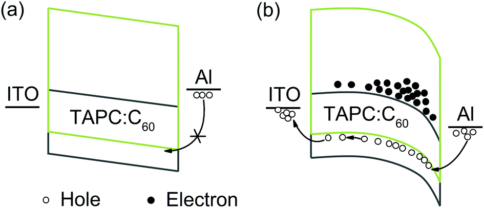 | ||
| Fig. 3 Energy band structures of the fabricated UV PM-type OPDs at reverse bias under (a) dark and (b) light conditions. The device structure is ITO/TAPC:C60 (50:1, 80 nm)/Al (100 nm). | ||
In order to reduce the dark current of the fabricated UV PM-type OPDs, we further studied the effect of the active layer thickness on the dark current of the device. As shown in Fig. 4a, as the thickness of the active layer increases, the dark current density of the device is significantly reduced because the hole transport is blocked. The active layer thickness increase from 100 nm to 250 nm causes the active layer near the Al electrode to absorb less light and accumulate fewer electrons. Thus, the EQEs of the devices gradually decrease with the increase of the active layer thickness, as shown in Fig. 4b, from 753655% to 560606%, 519949% and 375075%. At the same time, since R and EQE have a proportional relationship, increasing the thickness of the active layer also reduces the R of the device, as shown in Fig. 4c. However, the significantly reduced dark current greatly improves the D* of the devices, as shown in Fig. 4d, and the maximum D* of the devices increases from 5.9 × 10¹³ jones with a thickness of 100 nm to 1.5 × 10¹⁴ jones with a thickness of 200 nm. It is further observed that the full width at half maximum (FWHM) decreases as the thickness of the active layer increases. For example, the OPDs with 100 nm and 200 nm thickness of active layers have a corresponding FWHM of ∼36 nm and ∼27 nm, respectively. Since the penetration depth of different wavelength lights in the active layer is different, the penetration depth of the short-wavelength UV light is the shortest.46 Therefore, as the thickness of the active layer increases, the response of the devices to short-wavelength light gradually decreases, which is consistent with the CCN mechanism.47–49 Meanwhile, the cutoff wavelength of the spectral response of the devices is about 375 nm due to the limitation of the TAPC absorption spectrum. In addition, the transport of the holes injected by the tunneling process becomes slower due to the increase of the active layer thickness. The corresponding applied biases of the optimized devices for different active layer thicknesses are −16 V, −23 V, −30 V and −36 V, respectively. On the one hand, increasing the thickness of the active layer can effectively reduce the dark current density, thereby improving the detection performance of the devices. On the other hand, the thicker active layer will also increase the operating voltage of the devices, which is not conducive to practical applications. Therefore, the thickness of the active layer needs to be reasonably selected according to actual requirements.
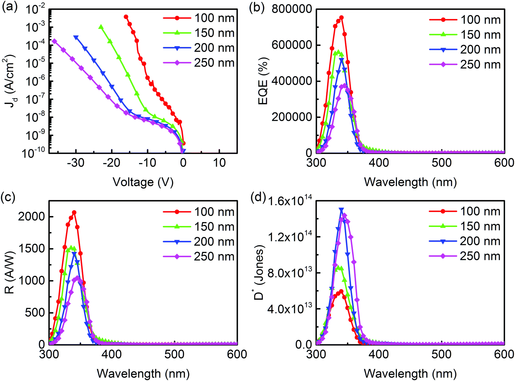 | ||
| Fig. 4 (a) Jd, (b) EQE, (c) R, and (d) D* characteristics of the fabricated UV PM-type OPDs with different active layer thicknesses. The device structure is ITO/TAPC:C60(50:1, 100 nm, 150 nm, 200 nm, 250 nm)/Al (100 nm). | ||
To investigate the repeatability and stability of the fabricated UV PM-type OPDs, we continuously fabricated 16 devices with the structure of ITO/TAPC:C60(50:1, 80 nm)/Al. Fig. 5 shows the statistical distribution in the EQE values of the devices under −14 V bias voltage. The maximum EQEs range from 700000% to 1200000%. According to the Gaussian function fitting result (shown as red curves), the average EQE value of the fabricated UV PM-type OPDs is around 950000%. Approximately 75% EQE values of the devices are located near the average value, indicating that the fabricated devices have excellent device-to-device uniformity and reproducibility. Moreover, we also find that the maximum EQE value of the devices shows negligible decay after 10 days of storage under ambient conditions, which indicates that the fabricated UV PM-type OPDs show good stability. In addition, a constant responsivity from weak light to strong light is important for photodetectors in a wide light intensity range in practical applications. As shown in Fig. S4 (ESI†), we characterized the photocurrent variation of the fabricated UV PM-type OPDs under UV light intensity ranging from 10−7 to 10−3 W cm−2 and −14 V applied voltage conditions. The fabricated UV PM-type OPDs show about 3 orders of magnitude linearly increasing response within the incident light intensity range from 1.2 × 10⁻⁶ to 1.5 × 10⁻³ W cm−2.
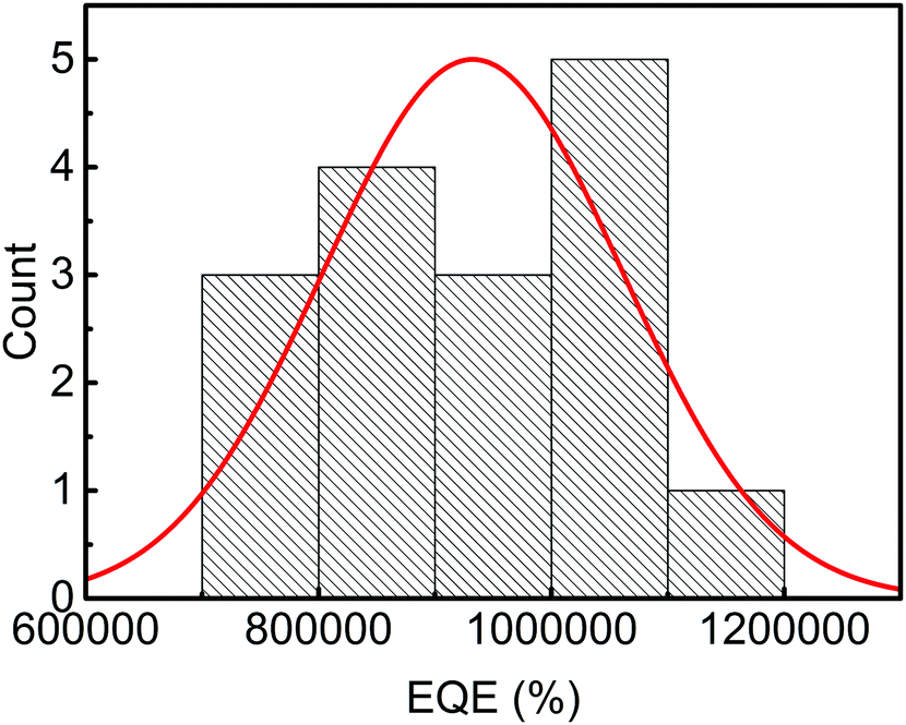 | ||
| Fig. 5 Statistical distribution in the EQE values of the 16 fabricated UV PM-type OPDs at the wavelength of 335 nm under the bias of −14 V. | ||
According to the PM mechanism, we know that the doping ratio of C60 in the active layer will affect the gain of the devices, and also determine the response in the visible light range. Fig. 6a shows the EQE curves of the resulting PM-type OPDs with four different active layer doping ratios. The device with the doping ratio of 50:1 exhibits the largest EQE among the four devices, which is consistent with previous reports.50,51 The device with the lowest C60 doping ratio of 200:1 exhibits the lowest EQE as fewer electrons are trapped on C60, which results in fewer hole tunneling injections from electrodes under light illumination. It can be seen that the EQE values decrease with the increase of C60 doping ratios, which should be attributed to the weakening of the hole tunneling injection and the decreasing of the hole mobility in the active layer with higher C60 concentration. Further increasing the doping ratio (10:1) will form continuous electron percolation pathways in the active layer, thereby giving the device no gain characteristics. UV/visible rejection ratio is defined as the ratio between the peak response and the response at longer visible wavelengths, which is also an important performance parameter for UV photodetectors. The donor/acceptor doping ratio will significantly affect the UV/visible rejection ratio of the devices. As shown in Fig. 6a, the doping ratios of 200:1, 100:1, 50:1 and 10:1 correspond to the rejection ratios (the ratio of EQE between 335 and 570 nm) of ∼2760, ∼1340, ∼620 and ∼50, respectively. Therefore, the response in the visible light range can be reduced by decreasing the C60 doping ratio, which helps to obtain more efficient visible blind UV OPDs. The rejection ratio of our fabricated PM-type OPDs is one of the best results in the reported UV response OPDs.12,52,53
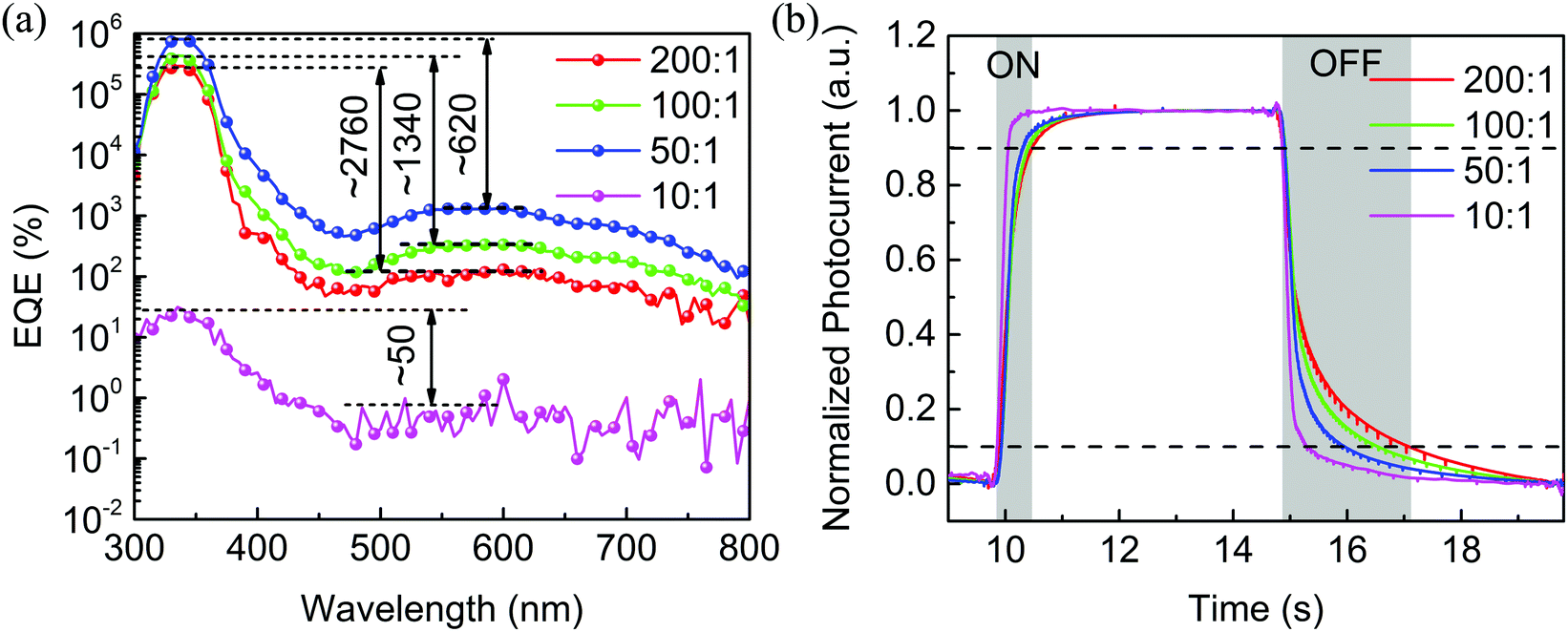 | ||
| Fig. 6 (a) EQE and (b) transient photocurrent responses of the fabricated OPDs with different donor:acceptor doping ratios at −14 V and 365 nm illumination. The pulse frequency is 0.1 Hz. The used device structure is ITO/TAPC:C60(200:1, 100:1, 50:1, 10:1, 80 nm)/Al. | ||
We further studied the effect of the active layer doping ratio on the transient photocurrent response of the resulting PM-type OPDs. The rise time (τr) is the time required for the photocurrent to rise from 10% of the stable value to 90%. The fall time (τf) is the time that it takes for the photocurrent to fall from 90% of the stable value to 10%. The transient response of the fabricated UV PM-type OPDs was measured by periodically turning on and off a 365 nm UV LED with modulated square waves (0.1 Hz). Fig. 6b shows the transient photocurrent characteristics of the devices with the doping ratios of 200:1, 100:1, 50:1 and 10:1. The τr values of the corresponding devices are 0.60 s, 0.48 s, 0.39 s and 0.19 s, and the τf values are 2.21 s, 1.63 s, 1.06 s and 0.43 s, respectively. It is shown that the response speed of the devices gradually becomes faster as the C60 doping ratio increases. For the resulting PM-type OPDs with the ratios of 200:1, 100:1 and 50:1, the photocurrent mainly comes from hole tunneling injection assisted by trapped electrons on C60 near the Al cathode. As the doping ratio of C60 in the active layer increases, sufficient electrons can be captured quickly. Therefore, the τr of the devices is gradually reduced. The τf mainly depends on the time required for the captured electrons to be released from C60 and transported to the electrode. The low C60 doping ratio will result in a slower electron transport speed due to fewer electron transport pathways. With the increase of the C60 doping ratio, the released electrons can be transported quickly to the corresponding electrode, thus shortening the fall time. For the photodiode type OPDs (10:1), the photocurrent mainly comes from the photogenerated exciton dissociation and charge carrier collection under reverse bias. Since there are no processes of trapping and releasing electrons, the τr and τf of the devices are relatively smaller. These results further indicate that the working mechanism of the fabricated UV PM-type OPDs is the trap-assisted hole tunneling injection model. Therefore, we can adjust the PM value, rejection ratio and response speed of the resulting UV PM-type OPDs by changing the C60 doping ratio in the active layer, thereby satisfying various application requirements.
In addition, we fabricated flexible visible-blind UV PM-type OPDs and flexible OLEDs based on a PET substrate, where the ITO electrodes (∼25 Ω sq−1) were prepared by magnetron sputtering. Then, as shown in Fig. 7a, we integrated the flexible visible-blind UV PM-type OPD with the flexible OLED to obtain a wearable UV monitoring display. Fig. 7b shows the configuration of the wearable UV monitor. The flexible UV PM-type OPD and the flexible OLED are connected in series via a conductive tape and then connected to a power supply through wires to form a complete circuit. Fig. 7c and d show the device structure of the flexible visible-blind UV PM-type OPD and OLED. The detailed device structures are as follows, PET/ITO/TAPC:C60 (50:1, 80 nm)/Al (100 nm), PET/ITO/HAT-CN (15 nm)/TAPC (50 nm)/TCTA (5 nm)/Bepp2:8 wt% Ir(ppy)2(acac) (15 nm)/Bepp2 (40 nm)/Liq (1.5 nm)/Al (100 nm). Since the flexible visible-blind UV PM-type OPD can generate enough photogenerated current under the applied bias voltage and UV illumination, it can drive the OLED to work well without an additional external current amplifier. Meanwhile, the flexible visible-blind UV PM-type OPD exhibits UV wavelength selective response characteristics, so that other wavelengths of light cannot cause the UV monitor to operate. To demonstrate these, we selected LEDs with different emission colours (UV, blue, green and red) to irradiate the flexible visible-blind UV PM-type OPD, and the results proved that the OLED can only be driven under UV irradiation conditions, as shown in the Supporting Video. Fig. 7e shows the photograph of the luminance variation of the OLED in the UV intensity range from 0 μW cm−2 to 400 μW cm−2. It can be clearly seen that the brightness of the OLED gradually becomes stronger as the UV intensity increases. Besides, the integrated wearable UV monitor also exhibits excellent weak light detection characteristics, which is mainly attributed to the PM characteristics of fabricated visible-blind UV OPDs.
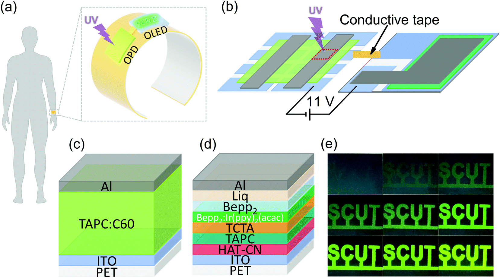 | ||
| Fig. 7 (a) Schematic illustration of the wearable UV monitor. (b) The composition and circuit connection of the UV monitor. The device structure of (c) flexible UV PM-type OPDs and (d) flexible OLEDs. (e) The photographs of wearable UV monitor under different UV light intensity. The UV light intensity was 0, 3.6, 6.9, 10.5, 14.4, 38.9, 69.1, 183, and 400 μW cm−2, respectively. | ||
Conclusions
Ultrahigh gain UV narrowband response PM-type OPDs have been successfully fabricated by the simple low concentration doping method of an acceptor in the donor. The fabricated devices showed a strong UV selective photoresponse from 300 nm to 370 nm with an FWHM of about 36 nm, which is mainly determined by the absorption characteristics of the donor materials. The optimized UV PM-type OPDs also exhibited an ultra-high EQE (1.08 × 10⁶%) and D* (1.28 × 10¹⁴ jones) at 335 nm wavelength. The devices prepared with several other wide bandgap organic semiconductor materials also exhibited good UV narrowband response characteristics, indicating that this device structure has wide applicability. Moreover, our research found that the doping ratio of donor and acceptor in the active layer has a great influence on the PM, rejection ratio and response speed of the devices. The rejection ratio of the optimized PM-type OPDs can exceed 103. In addition, we prepared a flexible visible-blind UV PM-type OPD and flexible OLED using PET substrates and integrated them into a wearable UV monitor, which can sensitively convert UV light into a visualized optical signal. Therefore, we believe that the realization of high-performance UV-sensitive PM-type OPDs has great potential applications in chemical and biological detection. Meanwhile, this design method can also be applied to fabricate various wavelength narrowband response PM-type OPDs by selecting different optical gap organic semiconductor materials as donor and acceptor.Conflicts of interest
There are no conflicts to declare.Acknowledgements
The authors gratefully acknowledge the National Natural Science Foundation of China (21788102, 51673067 and 51403203), Guangdong Provincial Key Laboratory of Luminescence from Molecular Aggregates, China (2019B030301003) and the Research Project of Jilin Province (20191102006YY) for the support of this research. Prof. Agafonov Vadim thanks the support of the Russian Ministry of Education and Science state assignment No. 3.3197.2017/&G.Notes and references
- M. R. Esopi, M. Calcagno and Q. M. Yu, Adv. Mater. Technol., 2017, 2, 1700025 CrossRef.
- Y. H. Lee, O. Y. Kweon, H. Kim, J. H. Yoo, S. G. Han and J. H. Oh, J. Mater. Chem. C, 2018, 6, 8569 RSC.
- X. K. Zhou, D. Z. Yang, D. G. Ma, A. Vadim, T. Ahamad and S. M. Alshehri, Adv. Funct. Mater., 2016, 26, 6619 CrossRef CAS.
- K. Zhang, L. Lv, X. F. Wang, Y. Mi, R. Q. Chai, X. F. Liu, G. Z. Shen, A. D. Peng and H. Huang, ACS Appl. Mater. Interfaces, 2018, 10, 1917 CrossRef CAS.
- J. L. Miao, F. J. Zhang, Y. Z. Lin, W. B. Wang, M. L. Gao, L. L. Li, J. Zhang and X. W. Zhan, Adv. Opt. Mater., 2016, 4, 1711 CrossRef CAS.
- B. Zhang, M. T. Trinh, B. Fowler, M. Ball, Q. Xu, F. Ng, M. L. Steigerwald, X. Y. Zhu, C. Nuckolls and Y. Zhong, J. Am. Chem. Soc., 2016, 138, 16426 CrossRef CAS PubMed.
- S. Yoon, K. M. Sim and D. S. Chung, J. Mater. Chem. C, 2018, 6, 13084 RSC.
- L. L. Li, Y. H. Deng, C. X. Bao, Y. J. Fang, H. T. Wei, S. Tang, F. J. Zhang and J. S. Huang, Adv. Opt. Mater., 2017, 5, 1700672 CrossRef.
- W. H. Li, H. Guo, Z. A. Wang and G. F. Dong, J. Phys. Chem. C, 2017, 121, 15333 CrossRef CAS.
- A. Armin, V. R. D. Jansen-van, N. Kopidakis, P. L. Burn and P. Meredith, Nat. Commun., 2015, 6, 6343 CrossRef CAS PubMed.
- W. B. Wang, F. J. Zhang, M. D. Du, L. L. Li, M. Zhang, K. Wang, Y. S. Wang, B. Hu, Y. J. Fang and J. S. Huang, Nano Lett., 2017, 17, 1995 CrossRef CAS.
- T. Zhu, J. Su, J. Alvarez, G. Lefèvre, F. Labat, I. Ciofini and T. Pauporté, Adv. Funct. Mater., 2019, 29, 1903981 CrossRef.
- M. R. Esopi, E. J. Zheng, X. Y. Zhang, C. Cai and Q. M. Yu, Phys. Chem. Chem. Phys., 2018, 20, 11273 RSC.
- J. X. Chen, Z. L. Li, F. L. Ni, W. X. Ouyang and X. S. Fang, Mater. Horiz., 2020, 7, 1828 RSC.
- F. W. Guo, B. Yang, Y. B. Yuan, Z. G. Xiao, Q. F. Dong, Y. Bi and J. Huang, Nat. Nanotechnol., 2012, 7, 798 CrossRef CAS PubMed.
- L. Shen, Y. J. Fang, H. T. Wei, Y. B. Yuan and J. S. Huang, Adv. Mater., 2016, 28, 2043 CrossRef CAS PubMed.
- L. Shen, Y. Zhang, Y. Bai, X. P. Zheng, Q. Wang and J. S. Huang, Nanoscale, 2016, 8, 12990 RSC.
- D. L. Shao, M. P. Yu, H. T. Sun, G. Q. Xin, J. Lian and S. Sawyer, ACS Appl. Mater. Interfaces, 2014, 6, 14690 CrossRef CAS PubMed.
- X. Y. Zhang, E. J. Zheng, M. R. Esopi, C. Cai and Q. M. Yu, ACS Appl. Mater. Interfaces, 2018, 10, 24064 CrossRef CAS PubMed.
- J. X. Wang, J. S. Chen, X. F. Qjao, S. M. Alshehri, T. Aharnad and D. G. Ma, ACS Appl. Mater. Interfaces, 2016, 8, 10093 CrossRef CAS PubMed.
- P. W. Liang, C. C. Chueh, S. T. Williams and A. K. Y. Jen, Adv. Energy Mater., 2015, 5, 1402321 CrossRef.
- F. W. Guo, Z. G. Xiao and J. S. Huang, Adv. Opt. Mater., 2013, 1, 289 CrossRef.
- W. B. Wang, F. J. Zhang, L. L. Li, M. L. Gao and B. Hu, ACS Appl. Mater. Interfaces, 2015, 7, 22660 CrossRef CAS PubMed.
- X. L. Li, S. R. Wang, Y. Xiao and X. G. Li, J. Mater. Chem. C, 2016, 4, 5584 RSC.
- S. Yoon, G. S. Lee, K. M. Sim, M. J. Kim, Y. H. Kim and D. S. Chung, Adv. Funct. Mater., 2021, 31, 2006448 CrossRef CAS.
- D. K. Neethipathi, H. S. Ryu, M. S. Jang, S. Yoon, K. M. Sim, H. Y. Woo and D. S. Chung, ACS Appl. Mater. Interfaces, 2019, 11, 21211 CrossRef CAS PubMed.
- D. C. Guo, D. Z. Yang, J. C. Zhao, A. Vadim and D. G. Ma, J. Mater. Chem. C, 2020, 8, 9024 RSC.
- L. L. Li, F. J. Zhang, W. B. Wang, Y. J. Fang and J. S. Huang, Phys. Chem. Chem. Phys., 2015, 17, 30712 RSC.
- Y. L. Wu, K. Fukuda, T. Yokota and T. Someya, Adv. Mater., 2019, 31, 1903687 CrossRef CAS PubMed.
- H. T. Wei, Y. J. Fang, Y. B. Yuan, L. Shen and J. S. Huang, Adv. Mater., 2015, 27, 4975 CrossRef CAS.
- Z. J. Lan, Y. L. Lei, W. K. E. Chan, S. M. Chen, D. Luo and F. R. Zhu, Sci. Adv., 2020, 6, eaaw8065 CrossRef CAS PubMed.
- Y. J. Fang, F. W. Guo, Z. G. Xiao and J. S. Huang, Adv. Opt. Mater., 2014, 2, 348 CrossRef CAS.
- H. W. Zan, W. W. Tsai and H. F. Meng, Appl. Phys. Lett., 2011, 98, 053305 CrossRef.
- W. Gong, T. An, X. Y. Liu and G. Lu, Chin. Phys. B, 2019, 28, 038501 CrossRef CAS.
- T. N. Wang, Y. F. Hu, Z. B. Deng, Y. Wang, L. F. Lv, L. J. Zhu, Z. D. Lou, Y. B. Hou and F. Teng, RSC Adv., 2017, 7, 1743 RSC.
- J. B. Wang, S. C. Chen, Z. G. Yin and Q. D. Zheng, J. Mater. Chem. C, 2020, 8, 14049 RSC.
- J. W. Lee, D. Y. Kim and F. So, Adv. Funct. Mater., 2015, 25, 1233 CrossRef CAS.
- F. B. Huang, X. Wang, K. Xu, Y. L. Liang, Y. Q. Peng and G. H. Liu, J. Mater. Chem. C, 2018, 6, 8804 RSC.
- D. Z. Yang, X. K. Zhou, Y. K. Wang, A. Vadim, S. M. Alshehri, T. Ahamad and D. G. Ma, J. Mater. Chem. C, 2016, 4, 2160 RSC.
- S. T. Chuang, S. C. Chien and F. C. Chen, Appl. Phys. Lett., 2012, 100, 013309 CrossRef.
- D. Z. Zhang, C. Y. Liu, K. Z. Li, S. P. Ruan, J. R. Zhou, X. D. Zhang and Y. Chen, J. Alloys Compd., 2019, 774, 887 CrossRef CAS.
- M. Azadinia, M. R. Fathollahi, M. Mosadegh, F. A. Boroumand and E. Mohajerani, J. Appl. Phys., 2017, 122, 154501 CrossRef.
- E. Y. Zheng, X. Y. Zhang, M. R. Esopi, C. Cai, B. Y. Zhou, Y. Y. Lin and Q. M. Yu, ACS Appl. Mater. Interfaces, 2018, 10, 41552 CrossRef CAS.
- G. MemİŞOĞLu and C. Varlikli, Turk. J. Electr. Eng. Co., 2016, 24, 4208 CrossRef.
- R. Dong, C. Bi, Q. F. Dong, F. W. Guo, Y. B. Yuan, Y. J. Fang, Z. G. Xiao and J. S. Huang, Adv. Opt. Mater., 2014, 2, 549 CrossRef CAS.
- D. Z. Zhang, R. L. Xu, L. Sun, C. Chen, F. L. Gao, X. D. Zhang, J. R. Zhou and S. P. Ruan, J. Phys. Chem. C, 2016, 120, 26103 CrossRef CAS.
- W. B. Wang, M. D. Du, M. Zhang, J. L. Miao, Y. Fang and F. J. Zhang, Adv. Opt. Mater., 2018, 6, 1800249 CrossRef.
- J. L. Miao, F. J. Zhang, M. D. Du, W. B. Wang and Y. Fang, Phys. Chem. Chem. Phys., 2017, 19, 14424 RSC.
- A. Yazmaciyan, P. Meredith and A. Armin, Adv. Opt. Mater., 2019, 7, 1801543 CrossRef.
- Z. H. Han, H. Zhang, Q. S. Tian, L. L. Li and F. J. Zhang, Sci. China: Phys., Mech. Astron., 2015, 58, 054201 Search PubMed.
- J. L. Miao, M. D. Du, Y. Fang and F. J. Zhang, Nanoscale, 2019, 11, 16406 RSC.
- H. W. Lin, S. Y. Ku, H. C. Su, C. W. Huang, Y. T. Lin, K. T. Wong and C. C. Wu, Adv. Mater., 2005, 17, 2489 CrossRef CAS.
- L. D. Wang, D. X. Zhao, Z. S. Su, F. Fang, B. H. Li, Z. Z. Zhang, D. Z. Shen and X. H. Wang, Org. Electron., 2010, 11, 1318 CrossRef CAS.
Footnote |
| † Electronic supplementary information (ESI) available. See DOI: 10.1039/d1mh00776a |
| This journal is © The Royal Society of Chemistry 2021 |