
 Open Access Article
 This Open Access Article is licensed under a
 Creative Commons Attribution 3.0 Unported Licence
Hidden spontaneous polarisation in the chalcohalide photovoltaic absorber Sn2SbS2I3†
Seán R.
Kavanagh
 ab,
Christopher N.
Savory
a,
David O.
Scanlon
*ac and
Aron
Walsh
*ad
ab,
Christopher N.
Savory
a,
David O.
Scanlon
*ac and
Aron
Walsh
*ad
aDepartment of Chemistry & Thomas Young Centre, University College London, 20 Gordon Street, London WC1H 0AJ, UK. E-mail: d.scanlon@ucl.ac.uk; a.walsh@imperial.ac.uk
bDepartment of Materials & Thomas Young Centre, Imperial College London, Exhibition Road, London SW7 2AZ, UK
cDiamond Light Source Ltd., Diamond House, Harwell Science and Innovation Campus, Didcot, Oxfordshire OX11 0DE, UK
dDepartment of Materials Science and Engineering, Yonsei University, Seoul 03722, Republic of Korea
First published on 5th July 2021
Abstract
Perovskite-inspired materials aim to replicate the optoelectronic performance of lead-halide perovskites, while eliminating issues with stability and toxicity. Chalcohalides of group IV/V elements have attracted attention due to enhanced stability provided by stronger metal-chalcogen bonds, alongside compositional flexibility and ns2 lone pair cations – a performance-defining feature of halide perovskites. Following the experimental report of solution-grown tin-antimony sulfoiodide (Sn2SbS2I3) solar cells, with power conversion efficiencies above 4%, we assess the structural and electronic properties of this emerging photovoltaic material. We find that the reported centrosymmetric Cmcm crystal structure represents an average over multiple polar Cmc21 configurations. The instability is confirmed through a combination of lattice dynamics and molecular dynamics simulations. We predict a large spontaneous polarisation of 37 μC cm−2 that could be active for electron–hole separation in operating solar cells. We further assess the radiative efficiency limit of this material, calculating ηmax > 30% for film thicknesses t > 0.5 μm.
New conceptsMixed-metal chalcohalides have emerged at the forefront of perovskite-inspired materials. A rigorous description of their atomistic properties and performance potential is lacking. In particular, Sn2SbS2I3 contains two lone-pair cations which are known to drive unusual structure–property relations. Using a range of first-principles modelling techniques, we reveal a spontaneous symmetry breaking away from the known non-polar crystal structure. We link this local polarisation, which was previously hidden to macroscopic diffraction techniques, to the high optoelectronic efficiency potential and defect-tolerant properties of this system. The results shine a spotlight on the largely-unexplored class of A2BCh2X3 mixed-metal chalcohalides. These are candidates for solution-processed ferroelectric and optoelectronic devices, with the substitutional flexibility for engineering band gaps, band energies, and lattice polarisation. |
The photovoltaic performance of lead-halide perovskites has spurred major research efforts toward the discovery of ‘perovskite-inspired materials’ (PIMs).1–3 Through the use of lead-free and stable alternative materials, PIMs aim to replicate the ability of halide perovskites to combine high optoelectronic performance with low-cost solution processing methods, while overcoming their infamous stability and toxicity drawbacks. The applications of PIMs are not solely limited to solar cell devices. In fact, these materials have seen successful implementation in a wide range of optoelectronic applications, such as light-emitting diodes, photocatalysts, radiation detectors, thin film transistors and memristors.1
A defining feature of halide perovskites is the combination of a lone-pair cation with a halide anion which can produce, inter alia, dispersive valence and conduction bands, defect tolerance, and strong dielectric screening.1,4 On the other hand, the soft metal-halide bonding contributes to the poor chemical and thermal stabilities of these materials.5 Chalcohalide PIMs offer a route around this issue, demonstrating remarkably higher air and water stability – due to the increased strength of metal-chalcogen bonding4,5 – while retaining the ns2 cation–halide anion combination. These materials have already demonstrated promising efficiencies (>4%1,6,7) alongside low-cost fabrication methods, representing a fertile area for stable, non-toxic high-performance solar cells.8 Further increases in power-conversion efficiencies (PCEs) will be required to achieve commercial viability.5
Here we focus on tin antimony sulfoiodide (Sn2SbS2I3). Olivier-Fourcade et al.9 reported the preparation and structural characterisation of Sn2SbS2I3 in 1980, determining an orthorhombic Cmcm space group using X-ray diffraction measurements. This work was followed up with single-crystal X-ray analysis by the same research group in 1984.10 Later, Dolgikh11 prepared both Sn2SbS2I3 and the isostructural, isoelectronic Pb2SbS2I3 compound and investigated the optical dielectric response. Then in 1990, Starosta et al.12 prepared both antimony sulfoiodide compounds and used photoconductivity measurements to determine optical band gaps of 1.5 and 2.0 eV for the Sn and Pb-based materials, respectively. They also discussed the seemingly anomalous trend of increased band gap with chemical substitution of heavier elements.
In a major breakthrough, Sn2SbS2I3 was recently reported to exhibit a photovoltaic efficiency exceeding 4% in the first experimental device fabrication.4 Nie et al. used a low-cost single-step deposition method and reported good stability under conditions of high temperature, humidity and illumination. The achievement of a power conversion efficiency exceeding that first reported for methylammonium lead-iodide (MAPI)13 is promising. While Sn2SbS2I3 has been known for several decades,9 it is now at the forefront of potential defect-tolerant PIMs for optoelectronic applications. In this work, we characterise the physical properties of Sn2SbS2I3 using ab initio methods in order to understand the atomistic origins of impressive PV performance, and to assess the efficiency potential going forward.
Computational methods
We employ a combination of methods to probe the static and dynamic crystal structure of Sn2SbS2I3, in addition to its electronic and optical properties. All base calculations were performed using Density Functional Theory (DFT) within periodic boundary conditions through the Vienna Ab Initio Simulation Package (VASP).14–17 After testing several DFT exchange–correlation functionals (Section S2.2, ESI†), the optB86b-vdW18 functional was chosen for geometry optimisation, yielding the closest agreement with experiment for the c/a lattice parameter ratio. The ability of this dispersion-corrected functional to incorporate van der Waals interactions in solids has been well demonstrated, yielding accurate predictions of lattice parameters in lone-pair materials.19–22 To calculate relative formation energies and the ferroelectric-switching barrier with accuracy beyond DFT, the Random Phase Approximation (RPA) to the correlation energy was employed, using electronic wavefunctions calculated with the HSE0623 screened hybrid DFT functional.24,25 The HSE06 functional, with full inclusion of spin–orbit coupling effects, was also used for calculations of optical and electronic behaviour – having been demonstrated to yield accurate predictions of band gaps in semiconductor materials.26,27 Comprehensive details of the computational implementation are provided in Section S1 of the ESI,† and all calculation data and analyses are provided in an online repository at doi.org/10.5281/zenodo.4683140.Structural analysis
Geometry optimisations were performed for Sn2SbS2I3 in both Cmcm and Cmc21 space groups, using the entries on the Materials Project repository28 as the starting points. The relaxed crystal structures and unit cell dimensions are provided in Fig. 1 and Table 1, respectively.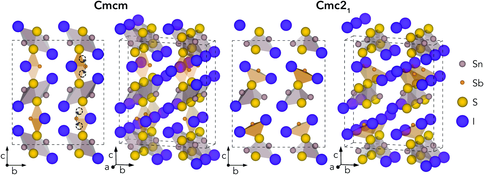 | ||
| Fig. 1 Calculated crystal structures for Cmcm and Cmc21 polymorphs of Sn2SbS2I3, in the conventional orthorhombic unit cell. Atoms sized according to their formal ionic radii. Curved arrows and empty circles indicate equivalent shifts in Sb position which correspond to the Cmcm to Cmc21 transition. | ||
| c/a | a/Å | b/Å | c/Å | Vol./Å3 | |
|---|---|---|---|---|---|
| Cmcm | 3.75 | 4.27 | 14.02 | 16.00 | 957.9 |
| Cmc21 | 3.85 | 4.29 | 14.31 | 16.51 | 1013.8 |
| Experiment | 3.85 | 4.25 | 13.99 | 16.38 | 973.9 |
The Cmcm structure comprises infinite chains of (Sn2S2I2)n along the a direction, tightly-packed along the b direction to form layers in the ab plane, with antimony and iodine atoms located between layers, yielding the overall (Sn2SbS2I3)n stoichiometry. The (Sn2S2I2)n chains are formed from face-sharing SnS3I2 pyramids, comprising a parallelepid base of S2I2 and an apical sulfur atom. In fact, this (Sn2S2I2)n structural motif matches the 1D chain structures of the AChX (A = Bi, Sb; Ch = S, Se; X = Br, I) ns2-cation chalcohalide family.29–32 Moving to the Cmc21 crystal structure, the coordination environments of Sb and (to a lesser extent) Sn shift to produce connected chains of the formula unit (Sn2SbS2I3)n along the a direction, as the Sb atoms attach to the (Sn2S2I2)n layers. The a and b cell lengths are similar for both polymorphs, with the greatest difference occurring along the c direction.
Much of the structural behaviour in this system is governed by the lone-pair activities of Sb(III) and Sn(II) cations. While the antimony cations are found to exhibit significant localisation of the ns2 electrons, only minimal distortion from spherical symmetry is witnessed for the Sn(II) lone-pair, due to a preferential alignment and thus enhanced interaction with anion p states (Section S3, ESI†). In both polymorphs, the Sb lone-pair is directed toward halide-bordered voids; either along the interchain gap (b direction) for Cmcm symmetry or toward the interchain gap (c direction) for Cmc21 – with more pronounced localisation visible in the Cmc21 case (Figs. S6–S8, ESI†). Indeed, this dynamic stereochemical activity of the Sb lone-pair is one of the primary driving factors behind the formation of the distorted, lower-symmetry Cmc21 polymorph – through a second-order Jahn–Teller instability, often observed in lone-pair chalcogenides.22,33–35
While all experimental works have reported the Cmcm crystal structure for Sn2SbS2I3,9,10,12 Ibanez et al.10 noted that assignment of Sb to an 8f Wyckoff position (i.e. the Sb Wyckoff site in Cmc21 symmetry) with 50% occupancy, as opposed to the 4c site for Cmcm, gave a significant reduction in R-factor – a measure of agreement between the structure model and diffraction data36 – from 0.105 to 0.066. Moreover, both Olivier-Fourcade et al.9 and Ibanez et al.10 observed large Debye–Waller (B) displacement factors for the Sb and Sn sites in Sn2SbS2I3 (i.e. the site positions which differ most between Cmcm and Cmc21 structures), even at temperatures as low as T = 173 K, alongside large anisotropy in the atomic displacement ellipsoids. Further structural and lone-pair analysis, with direct comparison to experiment (Fig. S4, ESI†), is provided in Sections S2 and S3 (ESI†).
Thermodynamic & dynamic stability
To ensure a high level of accuracy in the calculated phase stabilities, the Random Phase Approximation (RPA) to the correlation energy was employed. This beyond-DFT method has been demonstrated to yield predictions in excellent agreement with experimental results for the relative formation energies of structural polymorphs.1,38,39 With this method, the lower-symmetry Cmc21 phase was predicted to be the thermodynamically-favoured polymorph, with a formation energy 35.8 meV per atom below Cmcm.Further evidence of Cmcm instability was obtained by computing the phonon dispersions of both Sn2SbS2I3 polymorphs – shown in Fig. 2. Imaginary harmonic modes in the phonon dispersion (i.e. those with negative frequencies; ω < 0) indicate the presence of atomic displacements which lower the system energy. Two strong imaginary modes are witnessed in the Cmcm dispersion, demonstrating dynamic structural instability for this polymorph. Using the ISODISTORT40,41 package to visualise the imaginary-mode phonon eigenvectors, we confirm that these energy-lowering distortions correspond to different, equivalent Cmcm → Cmc21 structural transitions (Fig. S5, ESI†).
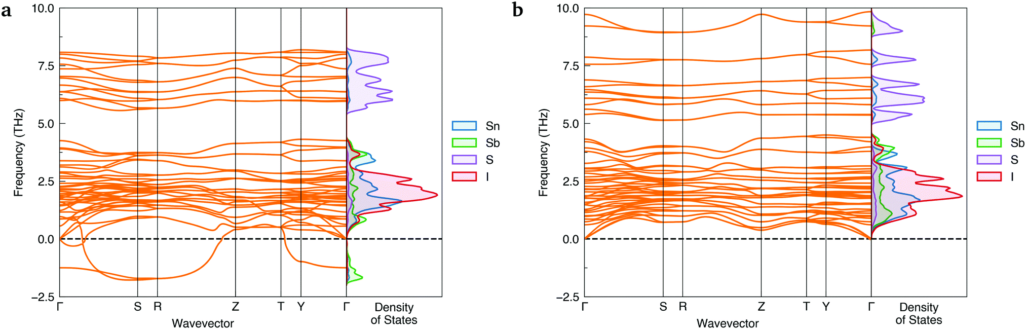 | ||
| Fig. 2 Simulated harmonic phonon dispersions of Sn2SbS2I3 in the Cmcm (a) and Cmc21 (b) crystal structures, alongside vertical plots of the atom-projected phonon density of states. Generated using ThermoPlotter.37 Brillouin zone path shown in Section S10a (ESI†). | ||
In contrast, no imaginary modes are observed for the Cmc21 polymorph. Thus we find the Cmc21 polymorph to exhibit both thermodynamic and dynamic stability, with converse behaviour for the Cmcm phase. We propose that experimental reports of centrosymmetric Cmcm Sn2SbS2I3 are the result of macroscopic averaging over locally non-centrosymmetric Cmc21 configurations. Similar to other ns2 cation materials,22,29,33 this polar phase behaviour is driven by a second-order (pseudo) Jahn–Teller instability, in which the off-centring of the Sb(III) ions leads to enhanced bonding interactions between the sp-hybridised Sb ns2 lone pair and the anion p states (yielding a small degree of Sb p character at 5 eV below the valence band maximum (VBM); Fig. 5a).
Spontaneous lattice polarisation
In the Cmc21 ground-state structure, the lack of inversion symmetry results in a spontaneous lattice polarisation ΔP = 37.0 μC cm−2 (calculated within the Berry phase formalism of the Modern Theory of Polarisation).42 The strong polarity places Sn2SbS2I3 next to the likes of ferroelectric oxide perovskites such as BaTiO3 (∼27 μC cm−2)43 and KNbO3 (∼30 μC cm−2), well above that of MAPbI3 (‘MAPI’)(4.4 μC cm−2)44 and the archetypal ‘photoferroic’ SbSI (11 μC cm−2).29,45 The mirror (m) and c-glide planes of the Cmc21 space group result in zero polarisation in the ab plane, with all electronic polarisation directed along the c axis, corresponding to the shift in Sb position indicated by the arrows in Fig. 1 and Fig. S5 (ESI†).We identify substantial mixed ionic-covalent bonding character in this system, reminiscent of that found in ns2-cation metal halides.1,32,46 Significant covalency is indicated by the cross-band-gap hybridisation of both cation p orbitals with both anion p orbitals, demonstrated by their overlap in both the conduction and valence bands (Fig. 5 and Fig. S13, S22, ESI†). Further evidence of enhanced orbital overlap is derived from the reduced cation–anion distances, relative to their ionic radii, save for the Sb–I pair (Table S1, ESI†). The resulting mixed ionic-covalent bonding gives rise to strong lattice polarisation, with large, anisotropic Born effective charges (Table 2) and dielectric tensor (εx,y,z = [51.3, 18.2, 22.4]).1,32,47,48
 ; |e|) for each atomic species in Sn2SbS2I3, calculated using the optB86b-vdW DFT functional.a The Born effective charge is a measure of the relationship between polarisation and atomic displacement, and is greater for the Cmcm phase due to structural instability.47,49 Comparison given to their formal oxidation states
| Species | Ox. state |
|
|
|
|---|---|---|---|---|
a Mean Born effective charges were calculated by taking the mean of the diagonal tensor component  for each atomic species. Full for each atomic species. Full  tensors for each symmetry-inequivalent species are provided in Table S6 (ESI). tensors for each symmetry-inequivalent species are provided in Table S6 (ESI).
|
||||
| Sn, Cmcm | +2 | +4.00 | +3.00 | +3.41 |
| Sn, Cmc21 | +2 | +4.07 | +3.16 | +2.77 |
| Sb, Cmcm | +3 | +6.82 | +3.55 | +9.08 |
| Sb, Cmc21 | +3 | +6.17 | +2.84 | +6.08 |
| S, Cmcm | −2 | −2.88 | −2.44 | −4.40 |
| S, Cmc21 | −2 | −2.69 | −2.47 | −3.50 |
| I, Cmcm | −1 | −3.03 | −1.55 | −2.10 |
| I, Cmc21 | −1 | −2.98 | −1.41 | −1.53 |
To calculate the barrier to polarisation switching, the Nudged Elastic Band (NEB)50 method was employed to map out the potential energy surface (PES) along the minimum-energy path between equivalent Cmc21 configurations (Fig. 3).
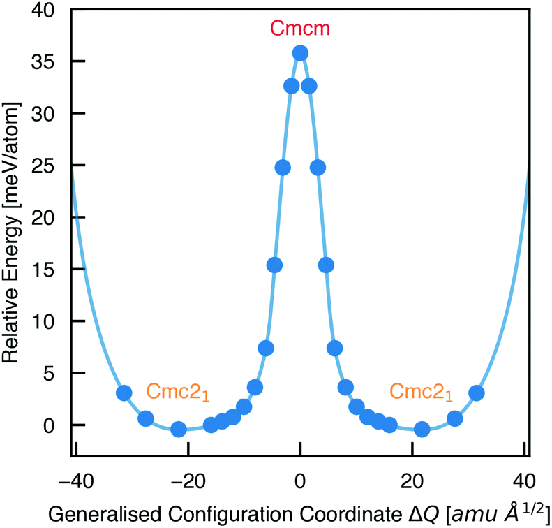 | ||
| Fig. 3 Potential energy surface along the configurational path between equivalent Cmc21 configurations of Sn2SbS2I3 (corresponding to the curved arrows in Fig. 1), calculated using the Nudged Elastic Band method.50 Filled circles represent calculated data points and the solid line is a spline fit. X axis given in units of mass-weighted displacement. | ||
We find that the Cmcm phase corresponds to the transition state between Cmc21 configurations, with no local stability around this saddle point on the PES. Consequently, the energetic barrier to ferroelectric switching corresponds to the relative energy of the Cmcm and Cmc21 polymorphs; ΔE = 35.8 meV per atom. This value gives rise to a moderate coercive field – calculated as 750 kV cm−1 for a single-crystal ferroelectric domain, using Landau theory (eqn (S1), ESI†).51 While the actual value will likely be at least an order of magnitude below this, due to a number of effects including domain formation, it places this material in a range intermediate between the weakly-polar lead-halide perovskites52 and the stronger oxide perovskites,51 as might be expected for a lone-pair chalcohalide material.
To demonstrate the stability of lattice polarisation at finite temperatures, we performed Molecular Dynamics (MD) simulations for Sn2SbS2I3 within an NVT ensemble at temperatures of 300 K and 500 K (Section S8, ESI†). Upon distortion from Cmcm to Cmc21, the two nearest-neighbour S atoms for Sb become inequivalent, forming short (in the polarisation direction) and long Sb–S bonds (Fig. 1 and Fig. S25, ESI†), allowing the polarisation dynamics to be visualised through the Sb–S bond lengths. As shown in Fig. 4, no appreciable swapping of the Sb–S bonds (corresponding to polarisation switching) is observed for the room-temperature MD runs, within the simulation timescale. On the other hand, transient hopping of Sb atoms occurs during the T = 500 K runs, as the material approaches a phase transition to higher-symmetry Cmcm (at which point the Sb–S bonds become equivalent and the probability densities merge; Fig. S25, ESI†), indicating a significant decrease in both the strength and stability of lattice polarisation at elevated temperatures. These results confirm the persistence of polar distortions at room temperature and dynamic fluctuations at 500 K. We cannot comment on the size of the polar domains that would be formed, however.
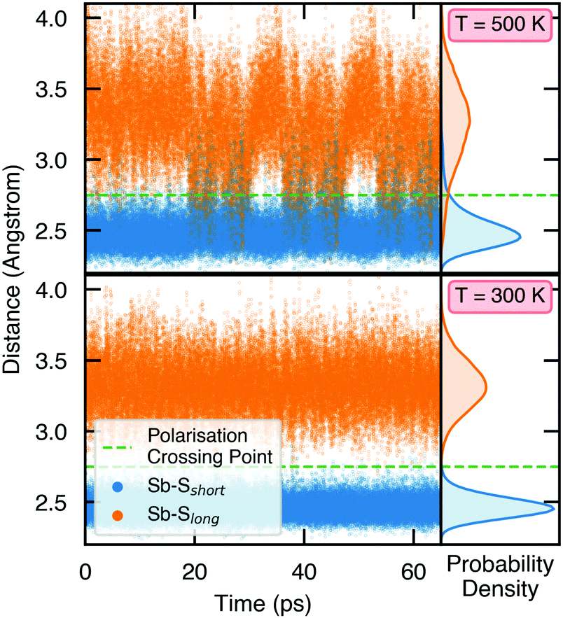 | ||
| Fig. 4 Variation of Sb–S bond lengths in Sn2SbS2I3 as a function of time during molecular dynamics simulations. The probability densities are shown on the right, given by 4πr2g(r), where g(r) is the radial distribution function. | ||
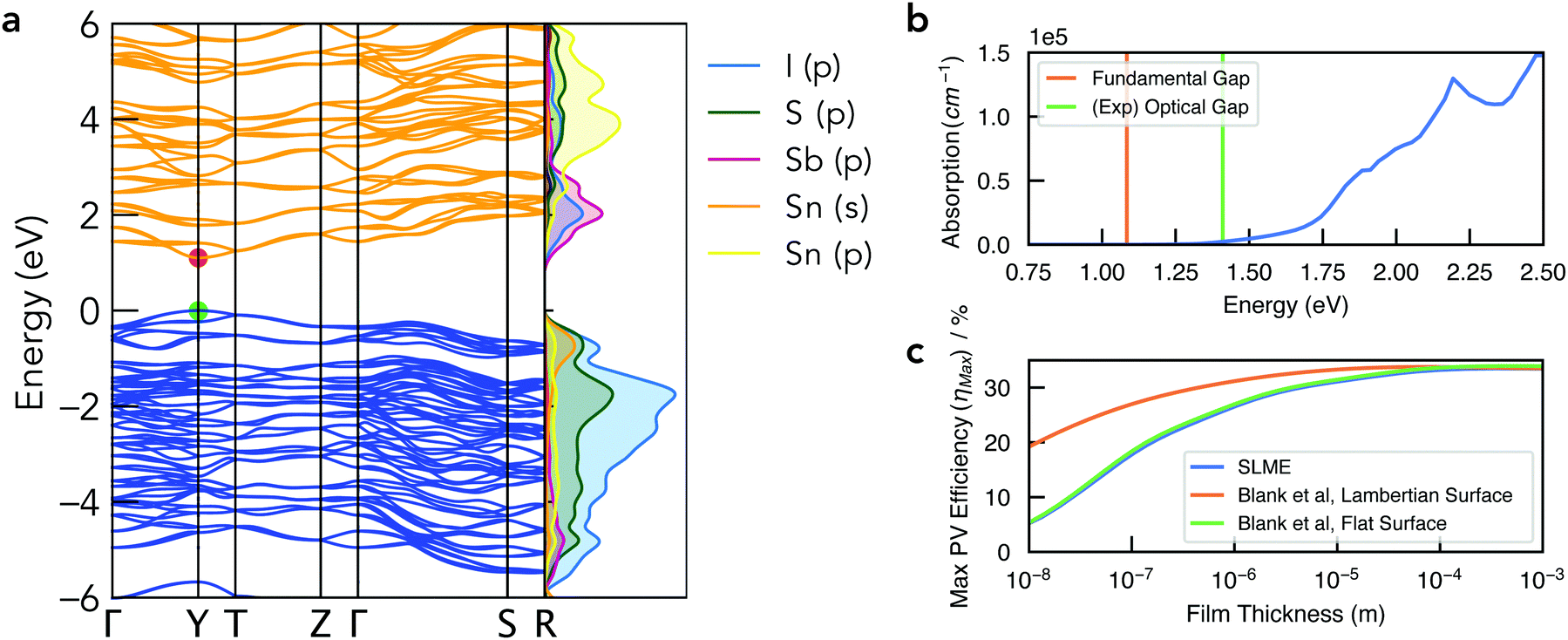 | ||
| Fig. 5 (a) Electronic band structure of Sn2SbS2I3 in the Cmc21 crystal structure, alongside a vertical plot of the orbital-projected electronic density of states, generated using sumo.59 Valence band in blue, conduction band in orange, and VBM set to 0 eV. Brillouin zone path shown in Fig. S10b (ESI†). (b) Absorption spectrum with vertical lines indicating the calculated electronic band gap and the experimental optical gap (Ref: Nie et al.4). Note that spectral smearing is expected under experimental measurement. (c) Maximum PV efficiency (ηmax) as a function of film thickness, using the SLME60 and Blank et al.61 estimates for the radiative limit (Qi = 1). | ||
The presence of this previously-hidden polar distortion in Sn2SbS2I3 poses several exciting prospects. In terms of PV applications, spontaneous polarisation can produce open-circuit voltages above the electronic band gap, via the Bulk Photovoltaic Effect, potentially allowing efficiencies above the standard limit for a single-junction solar cell.53–56 Moreover, the combination of ferroelectric behaviour and spin–orbit coupling could permit switchable spin texture for ‘ferroelectric Rashba semiconductor’ applications,57 while the effect on longitudinal optical (LO) phonons could favour polaron formation.58
Electronic structure
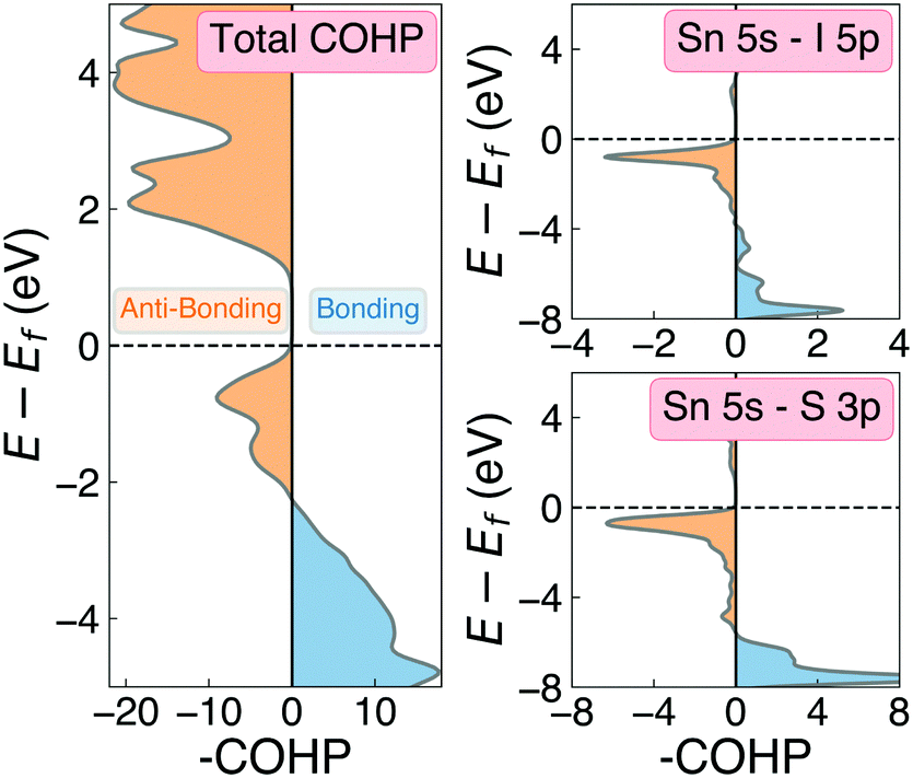
The electronic band structure of Cmc21 Sn2SbS2I3 is shown in Fig. 4. The band gap is direct, occurring at the Y high-symmetry k-point – which corresponds to maximum antiphase interactions along the conventional a crystal direction (i.e. along the (Sn2SbS2I3)n chains in Fig. 1). The fundamental energy gap is calculated as Eg = 1.08 eV, placing it in the ideal range for a photovoltaic absorber material, with a ‘detailed-balance’ efficiency limit of 32.5%.62As illustrated by the orbital-projected density of states and band-edge charge densities in Fig. 5a and Fig. S13, S14 (ESI†), the conduction band minimum (CBM) arises from Sb p–I p interactions, while the VBM is comprised of antibonding interactions between the Sn 5s2 lone pair and both anion p states (Fig. 6). Notably, this electronic structure allows the explanation of the reported ‘anomalous’ trend in band gap energies within the A2SbS2I3 (A = Sn, Pb) isostructure family, for which Starosta et al.12 found a gap 0.5 eV larger for the Pb-based compound. While band gaps of conventional semiconductors tend to decrease upon substitution of heavier elements, due to increased orbital energies, we witness a strong contradiction to this trend in this material class. This behaviour occurs due to the relativistic contraction of the Pb 6s orbitals, so that the Sn 5s states are in fact higher in energy,63 thus enhancing the anti-bonding interaction of the ns2 lone-pair with the anion p states at the VBM (Fig. 6).64 The result is a more disperse, higher-energy VBM with a reduced energy gap. See Section S6 (ESI†) for a discussion of the effects of spin–orbit interactions and the electronic structure of the Cmcm polymorph.
 | ||
| Fig. 6 COHP(E) cumulative (left) and Sn 5s – anion p orbital-decomposed (right) analysis of the electronic density of states in Sn2SbS2I3. Negative COHP values (blue) indicate energy-lowering, bonding-type interactions, while positive values (orange) indicate anti-bonding character. | ||
The optical absorption spectrum, shown in Fig. 4, exhibits a weak onset at the fundamental electronic band gap Eg = 1.08 eV. There are two primary origins of this behaviour. Firstly, we find a low electronic degeneracy at the band extrema (Fig. 5a and Fig. S16, S17, ESI†), itself a consequence of the low crystal symmetry, which rapidly increases with many more interband transitions available at E ≥ 1.4 eV. Another contributing factor is a weak transition dipole moment between the VBM and CBM electronic states (Fig. S15–S17, ESI†) – a consequence of both symmetry restriction and low spatial overlap. In the centrosymmetric Cmcm structure, the even (gerade) parity of both the VBM and CBM wavefunctions about the crystal inversion centre results in a formally symmetry-forbidden transition at the direct gap (as the electric dipole operator is of odd parity, thus yielding an overall zero optical transition matrix element; Section S6, ESI†). For the Cmc21 ground-state polymorph, this symmetry selection rule is broken by the shift in Sb positions (removing the inversion symmetry) as well as spin–orbit splitting, however these effects represent a relatively minor perturbation to the electronic structure (ΔEg,Cmcm![[thin space (1/6-em)]](https://www.rsc.org/images/entities/char_2009.gif) vs.Cmc21 = 0.03 eV; Fig. S11, ESI†). Consequently, while the direct VBM → CBM transition is no longer formally forbidden in the Cmc21 structure, the optical transition matrix element remains weak due to symmetry restraints, compounded by a spatial separation of the VBM and CBM states (Fig. S14, ESI†). The combination of a rapidly increasing joint density of states (JDOS) and optical transition dipole moment (TDM) at energies 0.3–0.5 eV above the direct band gap thus gives rise to a sharp increase in absorption coefficient at E ≥ 1.4 eV (Fig. 5b and Fig. S16, ESI†).
vs.Cmc21 = 0.03 eV; Fig. S11, ESI†). Consequently, while the direct VBM → CBM transition is no longer formally forbidden in the Cmc21 structure, the optical transition matrix element remains weak due to symmetry restraints, compounded by a spatial separation of the VBM and CBM states (Fig. S14, ESI†). The combination of a rapidly increasing joint density of states (JDOS) and optical transition dipole moment (TDM) at energies 0.3–0.5 eV above the direct band gap thus gives rise to a sharp increase in absorption coefficient at E ≥ 1.4 eV (Fig. 5b and Fig. S16, ESI†).
This behaviour, we propose, is a likely cause of the apparent mismatch between the calculated fundamental band gap (Eg = 1.08 eV) and that measured by optical spectroscopy (EOpt,Exp = 1.41 eV). While the slow onset of absorption renders the unambiguous determination of an optical gap difficult, Tauc-plot fitting of the calculated absorption within the 1–1.8 eV range gives a best linear fit (with R2 = 0.93) for an optical gap in the range 1.4–1.5 eV (Fig. S18, ESI†). Indeed, this plot closely resembles that measured by Nie et al.,4 who also reported a large Urbach energy of 464 meV – which may in part be an artefact of the slow absorption onset.
To quantify the efficiency potential of this material as a photovoltaic (PV) absorber, based on the calculated electronic and optical properties, the maximum PV efficiency (ηmax) as a function of film thickness was calculated using both the Spectroscopic Limited Maximum Efficiency (SLME)60 and Blank et al.61 metrics (Fig. 5c). As a consequence of the weak absorption onset, the attainable efficiency shows a strong dependence on film thickness, however this may be combatted through optimisation of the surface scattering properties. Using a Lambertian scattering surface, maximum efficiencies ηmax > 30% are achieved at thicknesses t > 0.5 μm, demonstrating the potential application of this material class in high-performance earth-abundant solar cells. Importantly, this model assumes the radiative limit (i.e. internal quantum luminescence efficiency Qi = 1), and so the presence of non-radiative recombination (Qi < 1) will act to reduce the achievable efficiency and lead to a distinct optimal thickness in the range 0.5–5 μm (Fig. S19, ESI†).
Potential for defect tolerance
One of the primary origins of non-radiative electron–hole recombination is defects in the bulk crystal and at interfaces. By introducing electronic states within the bandgap, defects can facilitate carrier trapping and annihilation, thus reducing the open-circuit voltage (Voc) and photovoltaic efficiency.65–67 A primary driving factor behind the surge in research interest for ns2-cation PIMs is their potential to exhibit defect tolerance – facilitating high efficiencies despite low-cost solution synthesis.1,68,69 Sn2SbS2I3 exhibits several material properties which are known to contribute to defect tolerance. Firstly, we find the cation s2 and anion p orbitals interact to produce a valence band maximum of anti-bonding character. This bonding behaviour is illustrated by the Crystal Orbital Hamiltonian Population70,71 (COHP) analysis shown in Fig. 6, which decomposes the electronic density of states into regions of bonding and anti-bonding orbital interactions. The cation ns2-anion p anti-bonding interaction produces a high energy VBM, with an ionisation potential of 5.06 eV (Fig. S9, ESI†) – less than that of MAPI (5.70 eV),72 SbSI (5.37 eV)30 and Sb2Se3 (5.13 eV),35 and slightly larger than that of FaSnI3 (4.88 eV)73 – favouring the formation of shallow acceptor defects which are innocuous to PV performance. The substantial mixed ionic-covalent character and lattice polarisability in Sn2SbS2I3, discussed previously, results in a strong dielectric screening (εx,y,z = [51.3, 18.2, 22.4]) that will limit the electrostatic interactions between defects and charge carriers, thus reducing the probability of carrier capture and trap-mediated recombination.1,32One-dimensional atomic chain structures, exhibited by this (Fig. 1) and related materials such as Sb2Se3,35 BiOI32 and SbSI,29,30 can yield benign grain boundaries, greatly reducing charge-carrier recombination in polycrystalline absorber materials.32,74 The small electronic band gap (Eg ∼ 1.1 eV), wide conduction and valence bands, and relatively small electron effective mass (me = 0.29) also favour defect-tolerant behaviour in this material.1 Indeed, the presence of moderate defect tolerance is partially suggested by the impressive PV efficiency (η > 4%) and photoluminescence lifetimes (>7 ns) obtained by Nie et al.4 in the first experimental device fabrication for this material.
In conclusion, we present a theoretical characterisation of the Sn2SbS2I3 photovoltaic absorber. While experimental investigations have reported a non-polar, centrosymmetric Cmcm crystal structure, we propose that this in fact represents a macroscopic average over multiple Cmc21 configurations. Crucially, this leads to the prediction of ferroelectricity, with promising implications for high-efficiency photovoltaic operation and other technological applications.
Through ab initio calculation of the electronic and optical properties, we identify an ideal electronic band gap for a photovoltaic absorber (Eg = 1.08 eV), with power-conversion efficiencies ηmax > 30% at the radiative limit. These features, alongside several properties related to ‘defect tolerance’, present a promising outlook for the potential application of both this material and other unexplored members of the A2BCh2X3 class. Considering only isoelectronic, earth-abundant and non-toxic substituents, there are in fact 36 possible elemental combinations for the quaternary group IV/V chalcohalide family (A = Sn, Ge; B = Sb, Bi; Ch = O, S, Se; X = I, Br, Cl) which may be synthesisable – the majority of which have not yet been investigated.‡ Thus the performance potential in this system opens a zoo of compositional permutations for solution-processed ferroelectric and optoelectronic devices.
Conflicts of interest
There are no conflicts to declare.Acknowledgements
Seán R. Kavanagh thanks Dr Bonan Zhu for help with using the AiiDA infrastructure, Gabriel Krenzer for advice regarding molecular dynamics simulations, and Matthew Okenyi for useful discussions regarding Landau theory of hysteresis behaviour. SRK acknowledges the EPSRC Centre for Doctoral Training in the Advanced Characterisation of Materials (CDT-ACM)(EP/S023259/1) for funding a PhD studentship. CNS is grateful to the Ramsay Memorial Fellowship Trust and UCL Department of Chemistry for the funding of a Ramsay Fellowship. DOS acknowledges support from the EPSRC (EP/N01572X/1) and from the European Research Council, ERC (Grant No. 758345). AW acknowledges support from a National Research Foundation of Korea (NRF) grant funded by the Korean Government (MSIT) (2018R1C1B6008728). We acknowledge the use of the UCL Grace High Performance Computing Facility (Grace@UCL), the Imperial College Research Computing Service, and associated support services, in the completion of this work. Via membership of the UK's HEC Materials Chemistry Consortium, which is funded by the EPSRC (EP/L000202, EP/R029431, EP/T022213), this work used the ARCHER UK National Supercomputing Service (http://www.archer.ac.uk) and the UK Materials and Molecular Modelling (MMM) Hub (Thomas – EP/P020194 & Young – EP/T022213).Notes and references
- Y.-T. Huang, S. R. Kavanagh, D. O. Scanlon, A. Walsh and R. L. Z. Hoye, Nanotechnology, 2021, 32, 132004 Search PubMed.
- M. Buchanan, Nat. Phys., 2020, 16, 996 Search PubMed.
- A. M. Ganose, C. N. Savory and D. O. Scanlon, Chem. Commun., 2017, 53, 20–44 Search PubMed.
- R. Nie, K. S. Lee, M. Hu, M. J. Paik and S. I. Seok, Matter, 2020, S2590238520304471 Search PubMed.
- R. Nie, R. R. Sumukam, S. H. Reddy, M. Banavoth and S. I. Seok, Energy Environ. Sci., 2020, 13, 2363–2385 Search PubMed.
- R. Nie, M. Hu, A. M. Risqi, Z. Li and S. I. Seok, Adv. Sci., 2021, 8, 2003172 Search PubMed.
- A. Zakutayev, J. D. Major, X. Hao, A. Walsh, J. Tang, T. K. Todorov, L. H. Wong and E. Saucedo, J. Phys.: Energy, 2021, 3(3), 032003 Search PubMed.
- Y. C. Choi and K.-W. Jung, Nanomaterials, 2020, 10, 2284 Search PubMed.
- J. Olivier-Fourcade, J. C. Jumas, M. Maurin and E. Philippot, Z. Anorg. Allg. Chem., 1980, 468, 91–98 Search PubMed.
- A. Ibanez, J.-C. Jumas, J. Olivier-Fourcade and E. Philippot, J. Solid State Chem., 1984, 55, 83–91 Search PubMed.
- V. Dolgikh, Izv. Akad. Nauk SSSR, Neorg. Mater., 1985, 21, 1211–1214 Search PubMed.
- V. I. Starosta, J. Kroutil and L. Beneš, Cryst. Res. Technol., 1990, 25, 1439–1442 Search PubMed.
- A. Kojima, K. Teshima, Y. Shirai and T. Miyasaka, J. Am. Chem. Soc., 2009, 131, 6050–6051 Search PubMed.
- G. Kresse and J. Hafner, Phys. Rev. B: Condens. Matter Mater. Phys., 1993, 47, 558–561 Search PubMed.
- G. Kresse and J. Hafner, Phys. Rev. B: Condens. Matter Mater. Phys., 1994, 49, 14251–14269 Search PubMed.
- G. Kresse and J. Furthmüller, Comput. Mater. Sci., 1996, 6, 15–50 Search PubMed.
- G. Kresse and J. Furthmüller, Phys. Rev. B: Condens. Matter Mater. Phys., 1996, 54, 11169–11186 Search PubMed.
- J. Klimeš, D. R. Bowler and A. Michaelides, Phys. Rev. B: Condens. Matter Mater. Phys., 2011, 83, 195131 Search PubMed.
- A. Lozano, B. Escribano, E. Akhmatskaya and J. Carrasco, Phys. Chem. Chem. Phys., 2017, 19, 10133–10139 Search PubMed.
- S. A. Tawfik, T. Gould, C. Stampfl and M. J. Ford, Phys. Rev. Mater., 2018, 2, 034005 Search PubMed.
- F. Tran, L. Kalantari, B. Traoré, X. Rocquefelte and P. Blaha, Phys. Rev. Mater., 2019, 3, 063602 Search PubMed.
- S. Jaśkaniec, S. R. Kavanagh, J. Coelho, S. Ryan, C. Hobbs, A. Walsh, D. O. Scanlon and V. Nicolosi, npj 2D Mater. Appl., 2021, 5, 1–9 Search PubMed.
- J. Heyd, G. E. Scuseria and M. Ernzerhof, J. Chem. Phys., 2003, 118, 8207–8215 Search PubMed.
- J. Harl, L. Schimka and G. Kresse, Phys. Rev. B: Condens. Matter Mater. Phys., 2010, 81, 115126 Search PubMed.
- M. Kaltak, J. Klimeš and G. Kresse, J. Chem. Theory Comput., 2014, 10, 2498–2507 Search PubMed.
- P. Borlido, J. Schmidt, A. W. Huran, F. Tran, M. A. L. Marques and S. Botti, npj Comput. Mater., 2020, 6, 1–17 Search PubMed.
- A. V. Krukau, O. A. Vydrov, A. F. Izmaylov and G. E. Scuseria, J. Chem. Phys., 2006, 125, 224106 Search PubMed.
- A. Jain, S. P. Ong, G. Hautier, W. Chen, W. D. Richards, S. Dacek, S. Cholia, D. Gunter, D. Skinner, G. Ceder and K. a. Persson, APL Mater., 2013, 1, 011002 Search PubMed.
- K. T. Butler, J. M. Frost and A. Walsh, Energy Environ. Sci., 2015, 8, 838–848 Search PubMed.
- K. T. Butler, S. McKechnie, P. Azarhoosh, M. van Schilfgaarde, D. O. Scanlon and A. Walsh, Appl. Phys. Lett., 2016, 108, 112103 Search PubMed.
- A. M. Ganose, K. T. Butler, A. Walsh and D. O. Scanlon, J. Mater. Chem. A, 2016, 4, 2060–2068 Search PubMed.
- H. Shi, W. Ming and M.-H. Du, Phys. Rev. B, 2016, 93, 104108 Search PubMed.
- A. Walsh, D. J. Payne, R. G. Egdell and G. W. Watson, Chem. Soc. Rev., 2011, 40, 4455–4463 Search PubMed.
- C. N. Savory and D. O. Scanlon, J. Mater. Chem. A, 2019, 7, 10739–10744 Search PubMed.
- C. H. Don, H. Shiel, T. D. C. Hobson, C. N. Savory, J. E. N. Swallow, M. J. Smiles, L. A. H. Jones, T. J. Featherstone, P. K. Thakur, T.-L. Lee, K. Durose, J. D. Major, V. R. Dhanak, D. O. Scanlon and T. D. Veal, J. Mater. Chem. C, 2020, 8, 12615–12622 Search PubMed.
- G. Rhodes, Crystallography Made Crystal Clear: A Guide for Users of Macromolecular Models, Elsevier, Amsterdam, 3rd edn, 2006 Search PubMed.
- K. B. Spooner, M. Einhorn and D. W. Davies, GitHub:SMTG_UCL/ThermoPlotter, 2020.
- R. L. Z. Hoye, P. Schulz, L. T. Schelhas, A. M. Holder, K. H. Stone, J. D. Perkins, D. Vigil-Fowler, S. Siol, D. O. Scanlon, A. Zakutayev, A. Walsh, I. C. Smith, B. C. Melot, R. C. Kurchin, Y. Wang, J. Shi, F. C. Marques, J. J. Berry, W. Tumas, S. Lany, V. Stevanović, M. F. Toney and T. Buonassisi, Chem. Mater., 2017, 29, 1964–1988 Search PubMed.
- J. Harl and G. Kresse, Phys. Rev. Lett., 2009, 103, 056401 Search PubMed.
- H. T. Stokes, D. M. Hatch and B. J. Campbell, ISODISTORT, ISOTROPY Software Suite.
- B. J. Campbell, H. T. Stokes, D. E. Tanner and D. M. Hatch, J. Appl. Crystallogr., 2006, 39, 607–614 Search PubMed.
- R. D. King-Smith and D. Vanderbilt, Phys. Rev. B: Condens. Matter Mater. Phys., 1993, 47, 1651–1654 Search PubMed.
- H. H. Wieder, Phys. Rev., 1955, 99, 1161–1165 Search PubMed.
- A. Stroppa, C. Quarti, F. De Angelis and S. Picozzi, J. Phys. Chem. Lett., 2015, 6, 2223–2231 Search PubMed.
- A. A. Grekov, A. I. Rodin and V. M. Fridkin, Appl. Phys. Lett., 1969, 14, 119–120 Search PubMed.
- J. M. Frost, K. T. Butler, F. Brivio, C. H. Hendon, M. van Schilfgaarde and A. Walsh, Nano Lett., 2014, 14, 2584–2590 Search PubMed.
- N. A. Spaldin, J. Solid State Chem., 2012, 195, 2–10 Search PubMed.
- D. H. Fabini, G. Laurita, J. S. Bechtel, C. C. Stoumpos, H. A. Evans, A. G. Kontos, Y. S. Raptis, P. Falaras, A. Van der Ven, M. G. Kanatzidis and R. Seshadri, J. Am. Chem. Soc., 2016, 138, 11820–11832 Search PubMed.
- J. Brgoch, A. J. Lehner, M. Chabinyc and R. Seshadri, J. Phys. Chem. C, 2014, 118, 27721–27727 Search PubMed.
- H. Jónsson, G. Mills and K. W. Jacobsen, Classical and Quantum Dynamics in Condensed Phase Simulations, World Scientific, 1998, pp. 385–404 Search PubMed.
- S. Song, H. M. Jang, N.-S. Lee, J. Y. Son, R. Gupta, A. Garg, J. Ratanapreechachai and J. F. Scott, NPG Asia Mater., 2016, 8, e242 Search PubMed.
- B. Chen, J. Shi, X. Zheng, Y. Zhou, K. Zhu and S. Priya, J. Mater. Chem. A, 2015, 3, 7699–7705 Search PubMed.
- I. Grinberg, D. V. West, M. Torres, G. Gou, D. M. Stein, L. Wu, G. Chen, E. M. Gallo, A. R. Akbashev, P. K. Davies, J. E. Spanier and A. M. Rappe, Nature, 2013, 503, 509–512 Search PubMed.
- P. S. Brody, Ferroelectrics, 1975 Search PubMed.
- T. S. Sherkar and L. J. A. Koster, Phys. Chem. Chem. Phys., 2016, 18, 331–338 Search PubMed.
- F. Zheng, H. Takenaka, F. Wang, N. Z. Koocher and A. M. Rappe, J. Phys. Chem. Lett., 2015, 6, 31–37 Search PubMed.
- S. Picozzi, Front. Phys., 2014, 2, 10 Search PubMed.
- C. W. Myung, J. Yun, G. Lee and K. S. Kim, Adv. Energy Mater., 2018, 8, 1702898 Search PubMed.
- A. M. Ganose, A. J. Jackson and D. O. Scanlon, J. Open Source Software, 2018, 3, 717 Search PubMed.
- L. Yu and A. Zunger, Phys. Rev. Lett., 2012, 108, 068701 Search PubMed.
- B. Blank, T. Kirchartz, S. Lany and U. Rau, Phys. Rev. Appl., 2017, 8, 024032 Search PubMed.
- W. Shockley and H. J. Queisser, J. Appl. Phys., 1961, 32, 510–519 Search PubMed.
- D. R. Lide, CRC Handbook of Chemistry and Physics, CRC Press, Florida, 84th edn, 2003 Search PubMed.
- Z. Li, S. R. Kavanagh, M. Napari, R. G. Palgrave, M. Abdi-Jalebi, Z. Andaji-Garmaroudi, D. W. Davies, M. Laitinen, J. Julin, M. A. Isaacs, R. H. Friend, D. O. Scanlon, A. Walsh and R. L. Z. Hoye, J. Mater. Chem. A, 2020, 8, 21780–21788 Search PubMed.
- S. R. Kavanagh, A. Walsh and D. O. Scanlon, ACS Energy Lett., 2021, 6, 1392–1398 Search PubMed.
- S. Kim, J. A. Márquez, T. Unold and A. Walsh, Energy Environ. Sci., 2020, 1481–1491 Search PubMed.
- C. Freysoldt, B. Grabowski, T. Hickel, J. Neugebauer, G. Kresse, A. Janotti and C. G. Van de Walle, Rev. Mod. Phys., 2014, 86, 253–305 Search PubMed.
- A. Walsh and A. Zunger, Nat. Mater., 2017, 16, 964–967 Search PubMed.
- R. C. Kurchin, P. Gorai, T. Buonassisi and V. Stevanović, Chem. Mater., 2018, 30, 5583–5592 Search PubMed.
- V. L. Deringer and R. Dronskowski, in Comprehensive Inorganic Chemistry II (Second Edition), ed. J. Reedijk and K. Poeppelmeier, Elsevier, Amsterdam, 2013, pp. 59–87 Search PubMed.
- R. Dronskowski and P. E. Bloechl, J. Phys. Chem., 1993, 97, 8617–8624 Search PubMed.
- K. T. Butler, J. M. Frost and A. Walsh, Mater. Horizons, 2015, 2, 228–231 Search PubMed.
- Z. Zhao, F. Gu, Y. Li, W. Sun, S. Ye, H. Rao, Z. Liu, Z. Bian and C. Huang, Adv. Sci., 2017, 4, 1700204 Search PubMed.
- Y. Zhou, L. Wang, S. Chen, S. Qin, X. Liu, J. Chen, D.-J. Xue, M. Luo, Y. Cao, Y. Cheng, E. H. Sargent and J. Tang, Nat. Photonics, 2015, 9, 409–415 Search PubMed.
- S. M. Islam, C. D. Malliakas, D. Sarma, D. C. Maloney, C. C. Stoumpos, O. Y. Kontsevoi, A. J. Freeman and M. G. Kanatzidis, Chem. Mater., 2016, 28, 7332–7343 Search PubMed.
Footnotes |
| † Electronic supplementary information (ESI) available: Additional structural, dielectric, electronic and optical analysis. See DOI: 10.1039/d1mh00764e |
| ‡ The substitution of Sn with Pb, Sb with Bi and S with Se has been demonstrated for Sn2SbS2I3.10–12,75 |
| This journal is © The Royal Society of Chemistry 2021 |