
 Open Access Article
 This Open Access Article is licensed under a
 Creative Commons Attribution 3.0 Unported Licence
Metastable Ta2N3 with highly tunable electrical conductivity via oxygen incorporation†
Chang-Ming
Jiang
 a,
Laura I.
Wagner
a,
Matthew K.
Horton
bc,
Johanna
Eichhorn
a,
Tim
Rieth
a,
Viktoria F.
Kunzelmann
a,
Max
Kraut
a,
Yanbo
Li
d,
Kristin A.
Persson
bc and
Ian D.
Sharp
*a
a,
Laura I.
Wagner
a,
Matthew K.
Horton
bc,
Johanna
Eichhorn
a,
Tim
Rieth
a,
Viktoria F.
Kunzelmann
a,
Max
Kraut
a,
Yanbo
Li
d,
Kristin A.
Persson
bc and
Ian D.
Sharp
*a
aWalter Schottky Institute and Physics Department, Technische Universität München, 85748 Garching, Germany. E-mail: sharp@wsi.tum.de
bEnergy Technologies Area, Lawrence Berkeley National Laboratory, Berkeley, CA 94720, USA
cDepartment of Materials Science and Engineering, University of California, Berkeley, Berkeley, CA 94720, USA
dInstitute of Fundamental and Frontier Sciences, University of Electronic Science and Technology of China, Chengdu 610054, P. R. China
First published on 1st April 2021
Abstract
The binary Ta–N chemical system includes several compounds with notable prospects in microelectronics, solar energy harvesting, and catalysis. Among these, metallic TaN and semiconducting Ta3N5 have garnered significant interest, in part due to their synthetic accessibility. However, tantalum sesquinitride (Ta2N3) possesses an intermediate composition and largely unknown physical properties owing to its metastable nature. Herein, Ta2N3 is directly deposited by reactive magnetron sputtering and its optoelectronic properties are characterized. Combining these results with density functional theory provides insights into the critical role of oxygen in both synthesis and electronic structure. While the inclusion of oxygen in the process gas is critical to Ta2N3 formation, the resulting oxygen incorporation in structural vacancies drastically modifies the free electron concentration in the as-grown material, thus leading to a semiconducting character with a 1.9 eV bandgap. Reducing the oxygen impurity concentration via post-synthetic ammonia annealing increases the conductivity by seven orders of magnitude and yields the metallic characteristics of a degenerate semiconductor, consistent with theoretical predictions. Thus, this inverse oxygen doping approach – by which the carrier concentration is reduced by the oxygen impurity – offers a unique opportunity to tailor the optoelectronic properties of Ta2N3 for applications ranging from photochemical energy conversion to advanced photonics.
New conceptsTransition metal nitrides represent a versatile chemical space for creating new functional materials with tunable properties for a variety of applications. However, synthetic inaccessibility greatly hampers the technological development of functional nitrides – not only does the strong bonding of N2 molecules introduce kinetic barriers during synthesis, but it also makes many nitride compounds metastable against decomposition. In this work, we leverage the stronger electronegativity of oxygen to inductively stabilize higher metal oxidation states, such that the metallic mononitrides are converted to nitrogen-rich and semiconducting polymorphs. With this concept, the metastable and rarely reported Ta2N3 can be directly prepared by reactive magnetron sputter deposition, with the intentional addition of O2 into the sputtering environment. On the other hand, the extent of oxygen incorporation can be controlled and used to tailor the optoelectronic properties of the parent nitride materials. Such dual role of oxygen, in both facilitating the formation of metastable nitrides and tuning their functional characteristics, opens avenues of developing the previously underexplored nitride chemical space. |
Introduction
Metal nitrides offer intriguing prospects for a variety of applications, including solid-state lighting,1 integrated circuits,2 thermoelectrics,3 superconductors,4 and photocatalysis.5–7 The moderate electronegativity of nitrogen (χN = 3.04), compared to oxygen (χO = 3.44), results in a mixed ionic/covalent bonding character in these compounds. For such nitrides, the strong electrostatic interaction between N3− and metal cations translates to higher lattice cohesive energies, which manifest in their mechanical hardness and refractoriness.8 On the other hand, the N 2p energy levels are located in closer proximity to the metal electronic states, thus giving rise to a higher degree of orbital hybridization and improved charge transport properties compared to the corresponding metal oxides. While metal oxides are typically dielectrics or semiconductors, the electronic structure of transition metal nitrides is strongly affected by the nitrogen content and spans from metallic to semiconducting. Mononitrides of early transition metal elements, such as TiN, ZrN and TaN, have been widely utilized as wear-resistant coatings and metal diffusion barriers in microelectronics, and their excellent electrical conductivities can be attributed to the partially occupied metal d states.9 In comparison, the nitrogen-rich compounds (e.g. Ti3N4, Zr3N4, and Ta3N5) that adopt the highest possible metal oxidation states are expected to behave as semiconductors due to the energy gap separating the N 2p states from the unoccupied metal d states.10 Therefore, transition metal nitrides represent a versatile and promising chemical space, from which new functional materials can be developed.Hundreds of metal nitride phases are predicted to be (meta)stable by density functional theory (DFT) computation and await experimental realization.11,12 The synthesis of N-rich metal nitrides, however, proves to be a challenging task for two reasons. First, formation of N-rich nitrides requires high metal oxidation states, which are not as readily achievable as in the corresponding oxides due to the electronegativity difference between nitrogen and oxygen. Accordingly, a common synthesis strategy is to form the corresponding oxide prior to the nitridation step, as in the case of converting Ta2O5 to Ta3N5 by ammonolysis.13 Second, N-rich nitrides generally have low formation enthalpies that originate from the strong bonding of N2 molecules (964 kJ mol−1).14 To overcome this, many chemical vapor deposition (CVD) techniques employ more reactive nitrogen precursors such as azide, urea, or ammonia for preparing nitride compounds. Alternatively, the low chemical reactivity of N2 can be overcome through high pressure and high temperature (HPHT) synthesis routes, which have successfully yielded selected N-rich metal nitrides, including Ti3N4 and Zr3N4,15,16 though this technique lacks industrial scalability and is largely incompatible with thin film synthesis. To navigate the underexplored nitride chemical space effectively, there is a pressing need to identify key experimental parameters for synthesizing N-rich transition metal nitrides at low process temperatures and pressures.
The binary Ta–N system has a rich phase diagram with a wide range of N/Ta stoichiometries and several phases possessing properties of significant technological relevance.17–19 Among these, the orthorhombic Ta3N5 represents the most N-rich phase with the highest possible +5 formal oxidation state of Ta. This n-type semiconductor features a 2.1 eV direct bandgap and suitable band edge positions for driving water splitting reactions. Thus, it has garnered extensive research interest for solar energy conversion.6,20–22 The most common synthesis method of Ta3N5 is through nitridation of Ta2O5 in an ammonia flow at 850–1000 °C, though recently there are reports of direct Ta3N5 thin film deposition via atomic layer deposition23 and reactive magnetron sputtering.24 In contrast, tantalum mononitride (TaN) can form different polymorphs, including the δ-, ε-, and θ-phases, which exhibit high electrical conductivities. Thin films of these materials are often prepared by reactive sputtering and are widely used as diffusion barriers between copper and silicon within integrated circuits. The possibility to form non-stoichiometric TaN by adding Ta or N vacancies should be noted, in that the composition range of TaNx can vary from x = 0.8 to 1.4.25 This is important since increasing the nitrogen content diminishes the Ta 5d orbital overlap and consequently reduces the electrical conductivity. As an even more metal-rich phase, β-Ta2N, can be obtained by sintering Ta in N2 or NH3. The structure of this compound can be depicted as an hcp tantalum lattice with nitrogen occupying half of the octahedral interstitial sites.26
Despite the scientific and technological advancements of these tantalum nitride compounds, tantalum sesquinitride (Ta2N3) remains relatively unexplored. The first report of Ta2N3 dates back to 1968 by Coyne et al.27 However, in the ensuing 50 years there have only been a handful of reports related to the cubic bixbyite phase of Ta2N3. For example, in 2016, Salamon et al. reported bixbyite Ta2N3 grown by reactive sputtering.28 They found that transport characteristics were dominated by a combination of nitrogen excess in as-grown material and grain boundary barriers that were modified as a function of the post-synthetic vacuum annealing temperature. In contrast to the report of Coyne, their experimental and computational results indicated that Ta2N3 exhibits metallic conduction. However, neither the role of incorporated oxygen within the Ta2N3 phase on electronic structure and transport, nor its critical impact on metastability were addressed in that work. In addition to bixbyite-type Ta2N3, orthorhombic η-Ta2N3 has been synthesized using the HPHT method.29 First principles calculations also predicted another tetragonal polymorph of Ta2N3 that undergoes phase transformation to η-Ta2N3 at 7.7 GPa.30 However, the present work will focus on the cubic bixbyite phase of Ta2N3, which can be deposited in thin film form. Given the technological importance of the Ta–N system for diverse applications, scalable synthesis and detailed characterization of this lesser-known cubic bixbyite Ta2N3 phase provides interesting prospects for creating tunable materials with intermediate properties for new applications, as well as for understanding the key factors that allow synthesis of such metastable nitride phases.
Herein, we report the non-equilibrium deposition of bixbyite-type Ta2N3 thin films by reactive magnetron sputtering and characterize their optoelectronic properties. We find that the formation of metastable Ta2N3 hinges upon the presence of a small amount (0.65%) of O2 in the process gas mixture, which provides an inductive effect to stabilize higher oxidation states of Ta and suppress formation of metallic TaN. The presence of O2 during synthesis leads to the incorporation of 11.6 at% oxygen in the as-grown films. However, we find that reactive annealing in NH3 can be applied to reduce the concentration of oxygen impurities. Optical and electrical measurements, supported by density functional theory, reveal that stoichiometric Ta2N3 is a degenerate semiconductor with a ∼1.9 eV internal bandgap. However, the effective electron density in the conduction band is greatly reduced by the incorporation of oxygen at structural vacancy sites. Using this inverse oxygen doping approach to compensate free carriers of the intrinsically metallic film, we demonstrate that a conductivity variation of seven orders of magnitude can be readily achieved via post-synthetic reactive annealing. Not only do these findings resolve previously conflicting reports regarding the electronic structure of Ta2N3, but they also allow the tuning of the electrical characteristics from metallic to semiconducting character by varying the oxygen content. Thus, Ta2N3 with controlled oxygen content represents a versatile system with tunable metallic and semiconducting character for potential applications ranging from advanced plasmonics to photoelectrochemical energy conversion.
Results and discussion
Fig. 1a illustrates the bixbyite structure (space group Ia![[3 with combining macron]](https://www.rsc.org/images/entities/char_0033_0304.gif) ) of Ta2N3, which can be considered as an ordered-defect variant of the CaF2-type. While in the fluorite structure every cation is equivalent and coordinated with 8 anions, in Ta2N3 there exist two types of six-fold N-coordinated Ta cations, which then stack to form an fcc array. Accordingly, the CaF2 unit cell is expanded to a 2 × 2 × 2 superstructure so that the ordered arrangement of unoccupied voids in the bixbyite structure is accounted for. For each Ta at the 8b Wyckoff site, there are two nitrogen atoms absent from the 16c sites along a body diagonal; for each Ta at the 24d site, the two structural nitrogen vacancies are located along a face diagonal. In the first report of Ta2N3, the authors indexed the X-ray diffraction pattern to an fcc unit cell with lattice constant a0 ∼ 5.011 Å.27 Electron diffraction identified additional peaks corresponding to lattice plane spacings of 4.08, 2.13, and 1.95 Å, which were originally assigned to impurity phases. Upon reexamination, it is clear that these diffraction peaks stem from the (211), (332), and (431) lattice planes of the bixbyite Ta2N3 (Fig. 1b)—the lowering of lattice symmetry gives rise to these weak peaks observed not only in the Ta2N3 diffraction pattern, but also in C-Y2O3, In2O3, and U2N3 that all adopt the same bixbyite structure.31–33 In 2004, Ganin et al. prepared a microcrystalline Ta2N3 thin film by plasma-enhanced CVD, and indexed it to the bixbyite structure for the first time with a lattice constant of 9.8205 Å.17
) of Ta2N3, which can be considered as an ordered-defect variant of the CaF2-type. While in the fluorite structure every cation is equivalent and coordinated with 8 anions, in Ta2N3 there exist two types of six-fold N-coordinated Ta cations, which then stack to form an fcc array. Accordingly, the CaF2 unit cell is expanded to a 2 × 2 × 2 superstructure so that the ordered arrangement of unoccupied voids in the bixbyite structure is accounted for. For each Ta at the 8b Wyckoff site, there are two nitrogen atoms absent from the 16c sites along a body diagonal; for each Ta at the 24d site, the two structural nitrogen vacancies are located along a face diagonal. In the first report of Ta2N3, the authors indexed the X-ray diffraction pattern to an fcc unit cell with lattice constant a0 ∼ 5.011 Å.27 Electron diffraction identified additional peaks corresponding to lattice plane spacings of 4.08, 2.13, and 1.95 Å, which were originally assigned to impurity phases. Upon reexamination, it is clear that these diffraction peaks stem from the (211), (332), and (431) lattice planes of the bixbyite Ta2N3 (Fig. 1b)—the lowering of lattice symmetry gives rise to these weak peaks observed not only in the Ta2N3 diffraction pattern, but also in C-Y2O3, In2O3, and U2N3 that all adopt the same bixbyite structure.31–33 In 2004, Ganin et al. prepared a microcrystalline Ta2N3 thin film by plasma-enhanced CVD, and indexed it to the bixbyite structure for the first time with a lattice constant of 9.8205 Å.17
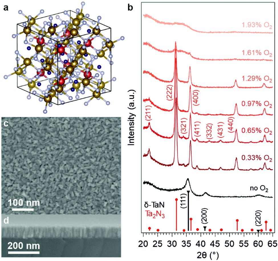 | ||
| Fig. 1 (a) Crystal model of bixbyite-type Ta2N3. The two non-equivalent Ta sites (Wyckoff 8b and 24d) are respectively labeled in red and brown, whereas nitrogen atoms are labeled in light gray. The structural nitrogen vacancy sites (Wyckoff 16c) are labelled as blue dots. The thin lines indicate the cubic unit cell of bixbyite with lattice constant a0 = 9.8205 Å. (b) Grazing-incidence XRD patterns of as-grown Ta2N3 thin films deposited by reactive magnetron sputtering with various amounts of O2 in the process gas mixture. Gray and red sticks: Bragg-reflection positions and intensities of δ-TaN and Ta2N3, respectively. (c) Plan view and (d) cross-sectional view SEM images of an as-grown Ta2N3(O) thin film. The sample was deposited on silicon at 500 °C growth temperature with 0.65% O2 in the process gas mixture. | ||
In this work, thin films of tantalum nitride were deposited on Si(100) and amorphous SiO2 substrates by reactive magnetron sputtering. This non-equilibrium deposition technique generates highly reactive atomic nitrogen by cracking N2 molecules with plasma, thus enabling metastable nitride phases to be synthetically accessed.34,35 The process gas comprised Ar and N2 (flow rate ratio 1![[thin space (1/6-em)]](https://www.rsc.org/images/entities/char_2009.gif) :2) with a ∼6.7 mTorr total pressure. Importantly, a controlled small dose of oxygen in the process gas mixture was found to be imperative to the formation of bixbyite Ta2N3. To investigate this, a series of thin films was grown at 500 °C with 0–1.9% O2 content in the process gas (Fig. 1b). In the absence of intentionally added oxygen, the appearance of the film was optically dense and metallic (Fig. S1 in ESI†), with X-ray diffraction (XRD) indicating formation of the δ-TaN phase. The film changed to a brown-orange color with merely 0.33% O2 present in the process gas. This optical change was accompanied by the evolution of the XRD pattern towards that of bixbyite Ta2N3. The highest crystallinity was obtained at 0.65% O2 concentration, which also yielded no residual δ-TaN phase. However, at higher oxygen flow rates, the weaker diffraction peaks that are unique for the low symmetry defect-ordered bixbyite structure were reduced and disappeared completely with 1.29% O2 in the process gas. At even higher oxygen concentrations, the films became amorphous, likely due to the formation of a disordered oxynitride. As discussed below, this finding is consistent with computational predictions of the above-hull energy of the stoichiometric Ta2N3O phase, which exceeds the tolerance of the system to form a metastable crystalline phase and instead favors a disordered amorphous phase.
:2) with a ∼6.7 mTorr total pressure. Importantly, a controlled small dose of oxygen in the process gas mixture was found to be imperative to the formation of bixbyite Ta2N3. To investigate this, a series of thin films was grown at 500 °C with 0–1.9% O2 content in the process gas (Fig. 1b). In the absence of intentionally added oxygen, the appearance of the film was optically dense and metallic (Fig. S1 in ESI†), with X-ray diffraction (XRD) indicating formation of the δ-TaN phase. The film changed to a brown-orange color with merely 0.33% O2 present in the process gas. This optical change was accompanied by the evolution of the XRD pattern towards that of bixbyite Ta2N3. The highest crystallinity was obtained at 0.65% O2 concentration, which also yielded no residual δ-TaN phase. However, at higher oxygen flow rates, the weaker diffraction peaks that are unique for the low symmetry defect-ordered bixbyite structure were reduced and disappeared completely with 1.29% O2 in the process gas. At even higher oxygen concentrations, the films became amorphous, likely due to the formation of a disordered oxynitride. As discussed below, this finding is consistent with computational predictions of the above-hull energy of the stoichiometric Ta2N3O phase, which exceeds the tolerance of the system to form a metastable crystalline phase and instead favors a disordered amorphous phase.
For the as-grown sample deposited with 0.65% O2 in the process gas mixture, SEM images revealed closely packed crystallites of ∼10 nm size that formed a homogeneous thin film covering the substrate (Fig. 1c). Cross-sectional imaging indicated that individual crystallites extend across the entire thickness of the film, suggesting a columnar growth mode (Fig. 1d). The compactness of the film was verified by X-ray reflectivity (XRR, Fig. S3, ESI†), which yielded a 10.64 ± 0.18 g cm−3 mass density that is only 6% smaller than the 11.33 g cm−3 bulk density of bixbyite Ta2N3. The film thickness, also determined via XRR, was 91.2 ± 0.3 nm for the 105 min growth time. In addition to SiO2 and Si substrates, the versatility of reactive magnetron sputtering also enabled the deposition of as-grown Ta2N3 thin films on GaN, Nb, and Ta substrates (Fig. S4, ESI†).
The X-ray diffractogram measured from the as-grown films resembled the reference bixbyite Ta2N3 pattern reported by Ganin et al.,17 albeit with smaller diffraction angles (Fig. 2a and Fig. S4, ESI†). Because of the presence of O2 during the reactive sputtering process, a certain quantity of oxygen is incorporated into the films, which consequently increases the unit cell volume and reduces the diffraction angles. Given that the O 2p states are located at energetically lower energies than the N 2p states, an increasing oxygen content in the film should push the valence band maximum downward and thus increase the bandgap. Indeed, the optical absorption onset moved monotonically toward shorter wavelengths with increasing O2 concentration in the process gas (Fig. S2, ESI†). To elucidate the role of oxygen incorporation on the optoelectronic properties of as-grown Ta2N3, quantitative elemental analysis was performed by combining Rutherford backscattering spectroscopy (RBS) and elastic recoil detection (ERD). The Ta, N, and O contents in the as-grown film deposited with 0.65% O2 in the process gas were found to be 33.3, 51.7, and 11.6 atomic%, respectively (Table S1, ESI†). Given that the 1.56 N/Ta ratio is already greater than the expected 1.50 value for stoichiometric Ta2N3, the oxygen in as-grown Ta2N3 is more likely to occupy interstitial sites rather than substituting nitrogen. Indeed, in the bixbyite structure, the structural nitrogen vacancies at the 16c Wyckoff sites are suitable for accommodating extra oxygen atoms, which would yield a Ta2N3O stoichiometry for the case of full oxygen occupancy. Starting with the unit cell parameters of bixbyite-type Ta2N3 that are published by Ganin et al.,17 we added an oxygen to the 16c site and then employed DFT to calculate the relaxed structure with the PBEsol36 energy functional (Table S2, ESI†). Not only does the resulting unit cell maintain a bixbyite-like diffraction pattern (Fig. S8, ESI†), the lattice constant also increases slightly to 9.9453 Å, consistent with the experimental observation. Therefore, the as-grown tantalum nitride film is hereafter referred as Ta2N3(O), indicating that the crystal structure resembles the bixbyite-type Ta2N3 but with oxygen predominantly occupying the structural nitrogen vacancies to varying degrees. To the best of our knowledge, such an ordered oxygen impurity incorporated variant of Ta2N3 has never before been reported.
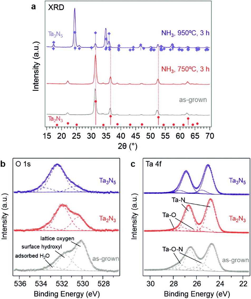 | ||
| Fig. 2 (a) XRD patterns of as-grown Ta2N3(O) on Si substrate and after NH3 annealing treatment at different temperatures. The blue and red sticks represent the reference pattern of orthorhombic Ta3N5 (PDF# 79-1533) and bixbyite-type Ta2N3, respectively. (b) O 1s and (c) Ta 4f region XPS spectra of the as-grown Ta2N3(O) and the Ta2N3 after NH3 annealing treatments. | ||
The chemical nature of O, Ta, and N in the as-grown Ta2N3(O) film was investigated by X-ray photoelectron spectroscopy (XPS). The main O 1s peak at a binding energy of ∼530.1 eV (Fig. 2b) has been previously assigned to lattice oxygen in Ta3N5, while the peaks at 531.6 eV and 532.8 eV are consistent with surface hydroxyl species and adsorbed water, respectively.37 The Ta 4f region exhibited a 1.9 eV spin–orbit splitting and can be deconvoluted to three spin–orbit split doublets. The first doublet at 24.7 and 26.6 eV represents the Ta2N3 phase, and the second doublet at 25.5 and 27.4 eV corresponds to a more highly oxidized state of tantalum arising from oxygen incorporation in the form of Ta2N3(O) oxynitride. The third doublet, with the highest binding energies at 26.2 and 29.1 eV, is consistent with the presence of a native tantalum oxide on the surface.
As described above, metallic δ-TaN is obtained if no O2 flow is used during the deposition, while amorphous oxynitride films are formed if the O2 flow is too high. Based on these results, we conclude that a small amount of oxygen was required to favor the formation of bixbyite-type Ta2N3 rather than δ-TaN during the reactive sputtering process. Interestingly, Rudolph et al. reported a similar phenomenon in the reactive sputter deposition of orthorhombic Ta3N5.24 In their work, the highest phase purity and crystallinity was achieved with 4.4 at% oxygen incorporated in the film through intentional addition of O2 in the process gas mixture. Both that work and the work presented here aim to synthesize N-rich tantalum nitride thin films by reactive sputtering in Ar/N2 mixtures, but the underlying reasons for the formation of two different phases (Ta3N5 and Ta2N3) are not immediately clear. The contrast may be attributed to the nucleation kinetics on the substrate, in that the initial seeding layer dictates the crystal phase in the following growth period. Nevertheless, in both cases the ability of a small amount of oxygen to transform δ-TaN into N-rich nitride phases is more than a coincidence. Analogous to the oxygen inductive effect in organic chemistry, it is hypothesized that lattice oxygen stabilizes Ta cations with formal oxidation states higher than the +3 state that is found in δ-TaN; for the cases of Ta3N5 and Ta2N3, average oxidation states of +5 and +4.5, respectively, must be chemically accessed.
We note that when sintering Ta2O5 in an NH3 atmosphere, completely eliminating oxygen anions has proven to be challenging. For example, Henderson et al. reported that the highest crystallinity of Ta3N5 obtained through ammonolysis contains 2.9 at% oxygen.38 The effects of oxygen substituent defects in Ta3N5 on electronic structure and photoluminescence have also attracted broad research interest.39 Rather than attempting to achieve pure nitride synthesis, we suggest that nitride-related research should leverage the impact of oxygen impurities in phase formation and stabilization, such that the transition metal nitride chemical space can be more effectively explored. However, as will be shown below, even a small amount of oxygen in the background can have a significant influence on the functional characteristics of tantalum nitrides. Given this dual role of oxygen, both in the synthesis of metastable nitrides and on their resulting electronic structure, establishing composition–structure–property relationships with a focus on the role of oxygen impurities within the parent material is key to the development of functional materials within this class. We note that the other Ta2N3 polymorph – the orthorhombic η-Ta2N3 obtained through the HPHT method – also contains oxygen impurities with an O/(N + O) ratio of ∼0.05.29 Interestingly, a related theoretical study indicated that oxygen substitution into nitrogen sites could enhance the structural stability of this metastable compound.40
With the critical role of oxygen in mind, a strategy for reducing incorporated oxygen from the as-grown Ta2N3(O) films was essential for allowing characterization of the optoelectronic properties of stoichiometric Ta2N3, as well as for isolating the impact of oxygen on these properties. To this end, reactive annealing in flowing NH3 at 750 °C for 3 h was performed and proved to be effective. After such a treatment, the X-ray diffraction peaks shifted to higher angles that are consistent with the previously reported 9.8205 Å lattice constant of bixbyite Ta2N3 (Fig. 2a). Moreover, XPS results indicated that both the 530.1 eV O 1s peak and the tantalum oxynitride doublet in the Ta 4f region were greatly diminished (Fig. 2b and c). Elemental analysis by RBS and ERD revealed the Ta, N, and O contents to be 28.5, 63.5, and 5.8 at% after NH3 annealing treatment at 750 °C (Fig. S7 and Table S1, ESI†). Even though the incorporated oxygen was not entirely eliminated, its content was reduced to the range commonly found in, for example, intensively studied Ta3N5 films. Therefore, the sample after ammonolysis at 750 °C is hereafter referred to as Ta2N3 in order to distinguish it from the as-grown Ta2N3(O). At annealing temperatures higher than 750 °C, phase transformation from bixbyite-type Ta2N3 to orthorhombic Ta3N5 was observed: a mixed-phase XRD pattern was obtained after annealing in flowing NH3 at 845 °C for 3 h (Fig. S9, ESI†), and at 950 °C the conversion to phase pure Ta3N5 was complete. In the latter case, the core level binding energies of the Ta 4f7/2 and 4f5/2 peaks related to Ta–N bonding were ∼0.25 eV higher than their counterparts in bixbyite Ta2N3 (Fig. 2c). This can be attributed to the higher average Ta oxidation state in Ta3N5 (+5) compared to Ta2N3 (+4.5). It is worth pointing out that even after ammonolysis at 950 °C, the orthorhombic Ta3N5 still contained residual oxygen, as demonstrated by the O 1s and Ta 4f XPS results (Fig. 2b and c). This observation, which is consistent with prior studies of Ta3N5, once again highlights the challenges in obtaining O-free but N-rich metal nitrides.
The optical absorption of as-grown Ta2N3(O) and Ta2N3 films were first analyzed by UV-vis spectroscopy. In order to eliminate thin film optical interference, both the transmission and reflectivity profiles were measured at a 15° angle of incidence, then the film absorbance was extracted (Fig. S11, ESI†). For both types of films, a strong absorption onset was observed at ∼650 nm (1.9 eV), though the Ta2N3 film exhibited a slightly sharper absorption edge following the reactive NH3 annealing treatment compared to the as-grown Ta2N3(O) sample. To achieve a higher dynamic range in analyzing the absorption coefficient, the background-free photothermal deflection spectroscopy (PDS) technique was used to probe the sub-bandgap region (Fig. 3a). The stoichiometric Ta2N3 film exhibits a Drude-like absorption feature that increases in strength towards lower photon energies. This phenomenon is consistent with free carrier absorption, and suggests a very high carrier concentration within the bixbyite Ta2N3. Interestingly, such a characteristic absorption feature was not observed for the as-grown Ta2N3(O) film that contained 11.6% lattice oxygen. Instead, a weaker sub-gap optical absorption that increased and plateaued with increasing photon energy was observed. Such an absorption feature, which is here found in the range of 0.6–1.5 eV, is consistent with optical transitions to or from electronic states within the bandgap. Hence, oxygen incorporation in Ta2N3 appears to significantly diminish the free carrier concentration within the material and the optical spectra of Ta2N3 and Ta2N3(O) resemble those of a degenerate and a non-degenerate semiconductor, respectively.
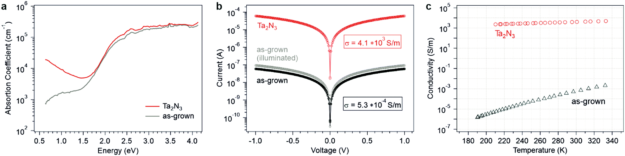 | ||
| Fig. 3 (a) Absorption coefficients of as-grown Ta2N3(O) and Ta2N3 measured by photothermal deflection spectroscopy. (b) Current–voltage characteristics (open circles) that were used to extract the in-plane electrical conductivities. (c) Temperature dependence of electrical conductivity on as-grown Ta2N3(O) and Ta2N3 films. | ||
To further understand the role of oxygen on the electronic properties of Ta2N3, in-plane electrical conductivity measurements were performed. For this purpose, interdigitated Ti/Au contacts (20/80 nm) were evaporated atop as-grown Ta2N3(O) (Fig. S12, ESI†). For Ta2N3 films after reactive annealing in NH3, a significantly increased conductivity was discernible by a handheld multimeter. Therefore, two Ti/Ta contacts (10/50 nm) separated by 5 mm were prepared. As shown in Fig. 3b, ohmic behavior was observed for both samples, albeit with a drastic difference in conductivity, σ, of 5.3 × 10⁻⁴ and 4.1 × 10³ S m−1 for the Ta2N3(O) and Ta2N3 films, respectively. In other words, reduction in oxygen content within the films caused an electrical conductivity enhancement by seven orders of magnitude. Although the polycrystalline nature of the thin films investigated here precluded reproducible and statistically meaningful quantification of carrier concentration, type, and mobility by Hall effect measurements, Ta2N3 films exhibited negative Seebeck coefficients, thus confirming their n-type character. Furthermore, light illumination gave rise to an additional photoconductivity for the as-grown Ta2N3(O) sample, but this phenomenon was absent from Ta2N3. This result is consistent with the Drude-like feature observed in optical absorption measurements and indicates that the background carrier concentration in Ta2N3 was much higher than the photoexcited carrier concentration.
The temperature-dependent conductivities of Ta2N3(O) and Ta2N3 are shown in Fig. 3c. For the case of Ta2N3(O), a strong temperature dependence with σ increasing from 1.5 × 10⁻⁶ S m−1 at 190 K to 2.1 × 10⁻³ S m−1 at 332 K was observed (Fig. 3c). In contrast, only a very weak temperature dependence (approximately a factor of two change) was observed for Ta2N3 over the same temperature range. Taken together, optical absorption, photoconductivity, and temperature-dependent transport data provide strong evidence that Ta2N3(O) behaves as a non-degenerate semiconductor, while Ta2N3 exhibits the characteristics of a metallic conductor. Thus, it appears that oxygen incorporation plays a major role in reducing the carrier concentration within the material and may be used to widely tune its electronic and transport properties across the metal-semiconductor transition.
To rationalize these findings regarding the intrinsic metallic nature of Ta2N3 and the role of oxygen as a compensating impurity dopant, the electronic structure of Ta2N3, as well as an idealized model Ta2N3O were calculated by density functional theory (DFT) using HSE06 hybrid functionals.41 The electronic band structures of these two compounds are generated with sumo42 and pymatgen43 and shown in Fig. 4a and b, with the zero of the energy scale set to the Fermi level. Both compounds exhibit a series of high-lying Ta 5d bands that are separated from N 2p bands by an approximately 1.1 eV energy gap. For the bixbyite-type Ta2N3, the Fermi level is located within the Ta 5d bands, which can be attributed to the average donation of half a valence electron per Ta atom due to its +4.5 average oxidation state within Ta2N3. This result is in excellent agreement with the experimental observations of the metallic character of Ta2N3. Indeed, considering the +4.5 average oxidation state of Ta, the n-type doping level in Ta2N3 should be on the order of 1022 cm−3 without accounting for electronically active structural defects or impurity doping, making it a degenerately-doped semiconductor.
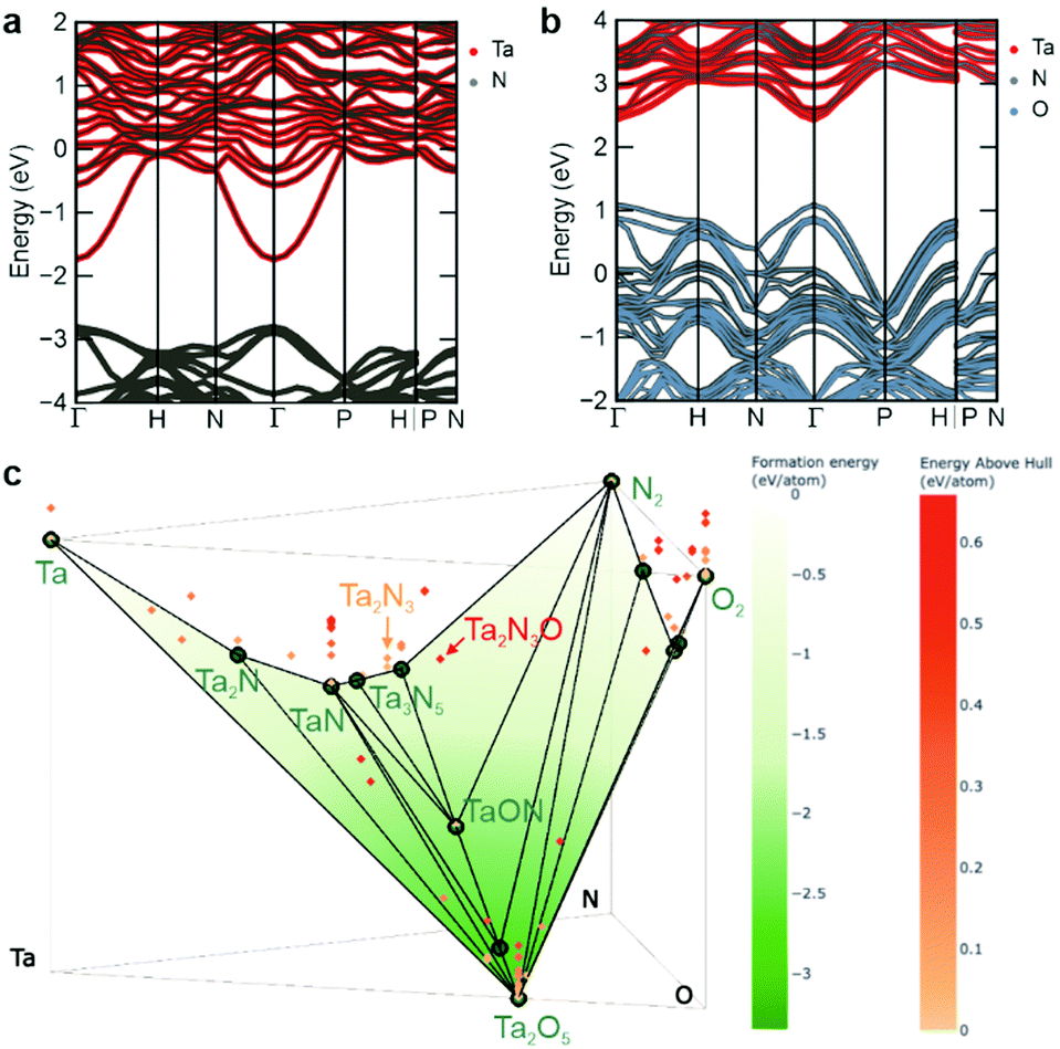 | ||
| Fig. 4 Predicted band structures for (a) bixbyite-type Ta2N3 and (b) Ta2N3O, where the oxygen atoms sit in interstitial positions, calculated by density functional theory using HSE06 hybrid functional. (c) Predicted convex hull phase diagram at 0 K for the Ta–N–O chemical system incorporating data from the Materials Project and supplemented with compatible data for the bixbyite-like Ta2N3 and Ta2N3O for the present work. | ||
Comparative evaluation of the predicted band structure for the model stoichiometric Ta2N3O compound, with all oxygen sitting at the ordered vacancy sites of the bixbyite structure reveals several important similarities and differences. Like Ta2N3, the Ta2N3O system is characterized by an 1.5 eV internal electronic bandgap. As expected from the relative energetic positions of N 2p and O 2p orbitals, the valence band maximum retains a dominant contribution from N 2p, while O 2p states are introduced deeper within the valence band. Although metallic character is also predicted for Ta2N3O, the Fermi level shifts downwards from the Ta-dominant conduction band into the lower energy N/O dominant valence band of the material, indicating p-type metallic conduction. However, it should be noted that since this calculation is performed for the idealized oxynitride system possessing full oxygen occupation of all ordered vacancy sites of the bixbyite structure, it represents the maximum electronic structure change and Fermi level shift that can be expected for oxygen incorporation into Ta2N3. At intermediate oxygen content, the Fermi level is predicted to lie within the bandgap. Interestingly, this provides the prospect not only for oxygen to drive the system across the metal-to-semiconductor transition, but also to modulate the conductivity from n-type to p-type as the oxygen content increases. In contrast to conventional doping, such strong conductivity changes are expected to occur at very high oxygen concentrations, where there is a concomitant change of the electronic structure of the material itself. In the ternary ZnSnN2 system that adopts the wurtzite structure, Pan et al. suggested that oxygen impurity could pair with excess Zn defects and thus lower the net doping concentration from 1020 to 1017 cm−3 range in highly off-stoichiometric material.44 Kim et al. have also reported the similar compensation effect of lattice oxygen on Mg-rich MgZrN2 with NaCl-like structure.45 These results, together with the drastic modification to the Ta2N3 electronic structure by interstitial oxygen incorporation presented in this work, highlight the potential in designing functional transition metal nitrides with desired electronic properties via controlling the oxygen impurity content, as well as configurational disorder related to both cations and anions.
Despite the intriguing electronic structure computed for the idealized Ta2N3O oxynitride phase, no experimental evidence for its formation or for metallic conduction with increasing oxygen content were observed under any processing conditions. Indeed, as described above, introduction of additional oxygen into the process gas eventually resulted in decreasing structural quality of films and the ultimate formation of amorphous material. To better understand this synthetic inaccessibility of stoichiometric and crystalline Ta2N3O, DFT was used to compute the energy landscape for the ternary Ta–N–O system at 0 K. Fig. 4c shows a phase diagram representing the formation energy as a function of composition (incorporating data from the Materials Project46), with thermodynamically stable compounds indicated as solid green points. Higher energy phases, which may be either metastable or unstable (see below), are indicated as red shaded points lying above the hull. Interestingly, both Ta2N3 and Ta2N3O are predicted to be thermodynamically unstable, with above-hull energies of 0.11 and 0.61 eV per atom, respectively.
An important feature of nitride compounds is their exceptionally large energetic window of metastability, which originates from the high cohesive energy of metal–nitrogen bonds.8 By comparison, oxides exhibit a much smaller energetic range over which metastable phases can be realized. To quantify this, the so-called amorphous limit was recently established.47 In particular, by comparing the free energies of crystalline phases to the corresponding amorphous state it is possible to quantify the energetic windows of synthetically accessible crystalline polymorphs of metastable compounds. In this context, the amorphous limit for TaN is comparatively large, with a computed value of 0.46 eV per atom, while the limit for Ta2O5 is 0.2 eV per atom. Using these representative values, we conclude that the above-hull energy of Ta2N3 of 0.11 eV per atom falls well within the energetic range of synthetically accessible compounds, while the corresponding value of 0.61 eV per atom for Ta2N3O significantly exceeds the expected amorphous limit. This prediction is in excellent agreement with our experimental findings, in which crystalline Ta2N3 and Ta2N3(O) compounds can be synthesized using the non-equilibrium reactive sputtering approach. However, with increasing oxygen introduced to the system, amorphous films, rather than crystalline Ta2N3O are observed (Fig. 1b).
To further explore the metastability of these compounds, the influence of growth temperature on film structure was investigated. In general, as temperature increases, entropic contributions to the free energy will increasingly favor the amorphous state of matter. Thus, the 0 K calculations of free energies of amorphous versus crystalline polymorphs provide a good indication of the amorphous limit and the basic feasibility of a metastable material to be synthesized. However, at increasingly high temperatures, metastable phases can become kinetically unlocked and films will be driven towards lower energy states, either via phase segregation or via amorphization. Fig. 5a shows the experimental XRD patterns collected as a function of growth temperature between 400 and 800 °C. In contrast to the conventional structure zone model, XRD measurements revealed that the film crystallinity reached a maximum at 500 °C, above which an increasingly intense amorphous background between 2θ = 32–35° was observed. This change was accompanied by the appearance of a new diffraction peak at 35.5°, which can be assigned to the (111) reflection of δ-TaN. Consistent with this assignment, XPS analysis of the sample gown at 800 °C was characterized by an additional lower binding energy doublet at 23.2 and 25.1 eV in the Ta 4f region, which indicates the presence of the lower Ta3+ oxidation state of δ-TaN (Fig. S14, ESI†).
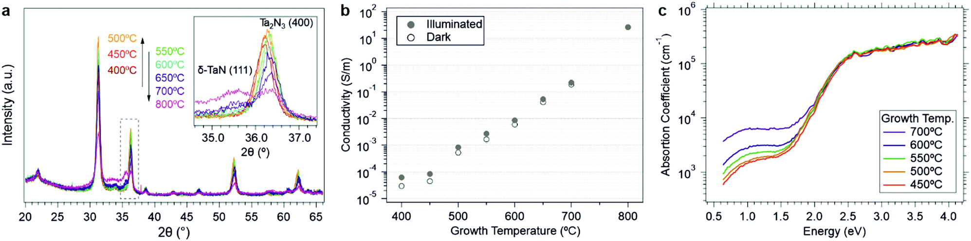 | ||
| Fig. 5 (a) XRD patterns of as-grown Ta2N3(O) films deposited at different substrate temperatures. Inset: Enlarged region of Ta2N3(400) diffraction peaks and the impurity peak associated with δ-TaN(111) diffraction. (b) Measured in-plane electrical conductivities of as-grown Ta2N3(O) films with different growth temperatures. (c) Absorption coefficients of as-grown Ta2N3(O) films, measured by photothermal deflection spectroscopy, as a function of growth temperature. | ||
Along with the emergence of the δ-TaN and amorphous phases at growth temperatures >500 °C, a monotonic shift of the remaining bixbyite Ta2N3 diffraction peaks toward larger angles was also identified by XRD (Fig. 5a). Since oxygen incorporation into the bixbyite structure leads to unit cell expansion, the smaller lattice constant at increasing growth temperature suggests reduced oxygen content within the remnant crystalline Ta2N3(O). Such a finding would be consistent with local compositional inhomogeneities, which result in stronger driving forces for amorphization in oxygen-rich regions and retention of Ta2N3 in oxygen deficient regions. While verification of this hypothesis will require future (spectro-)microscopic investigations of the material, our observation is that high growth temperature drives the system towards a phase segregated amorphous state with increasingly large concentrations of the thermodynamically stable δ-TaN phase. This is in excellent agreement with theoretical calculations of the metastability of bixbyite Ta2N3 and Ta2N3O, as well as the prior report of Ta2N3 decomposition into δ-TaN above 750 °C.19
Investigations of the optoelectronic properties of Ta2N3(O) films as a function of growth temperature provide additional support for the conclusions derived from the structural study described above, as well as opportunities for broadly tailoring film properties. As shown in Fig. 5b (and in Fig. S13, ESI†), the conductivity σ increased from 2.92 × 10⁻⁵ to 26.2 S m−1 – a six order of magnitude variation – when the growth temperature was raised from 400 to 800 °C. Corresponding PDS data reveal that the sub-bandgap absorption strength increased with the growth temperature (Fig. 5c). These trends with growth temperature are consistent with the structural results described above and may be described by two parallel factors: (i) the increasing fraction of metallic δ-TaN at temperatures above 500 °C, as detected by the emergence of the (111) δ-TaN diffraction peak, and (ii) the reduced oxygen content in the crystalline Ta2N3(O) phase fraction with increasing temperature, as detected by the shifting of Ta2N3(400) peak to larger angles.
These two parallel effects of oxygen incorporation and phase segregation can explain prior discrepancies in the reported optoelectronic properties of bixbyite Ta2N3, which include differing assignments of the material as a semiconductor or a metal. In the first account by Coyne et al. in 1968,27 an optical bandgap varying between 1.95 and 2.57 eV and a 0.1–0.3 eV energy barrier for electrical conduction were described, leading to the conclusion that the material is a semiconductor. In contrast, Ganin et al. reported their Ta2N3 thin films to be black in color and metallically conducting.17 Our results confirm that bixbyite Ta2N3 is a metastable compound exhibiting strong optical absorption above an ∼1.9 eV onset, but is intrinsically a metallic conductor with its Fermi level lying within the conduction band. Our observation that oxygen impurities can induce a metal-to-semiconductor transition can account for the conflicting assignment of the electronic nature of the material. Furthermore, we note that the existence of a window of transparency for our NH3-annealed Ta2N3 film in the near infrared range is in accordance with the degenerate nature of the material and may provide opportunities for its use as a semi-transparent contact layer. Likewise, the ability to extend this transparency window while controllably reducing its electrical conductivity suggests potential applications for the creation of tailored photonic systems. Moreover, the ∼1.9 eV optical absorption onset and highly tunable conductivity of Ta2N3 offer intriguing prospects for solar energy conversion applications. Preliminary tests using as-grown semiconducting Ta2N3(O) as a photoelectrode revealed that the material is photoactive (Fig. S15, ESI†). An anodic photocurrent onset was observed at ∼0.8 V vs. RHE in the presence of 0.1 M K4Fe(CN)6 as a sacrificial hole acceptor, consistent with the n-type character of the film. While the ∼5 μA cm−2 photocurrent density is much lower than possible for a material with such an absorption characteristic, we note that this result was achieved with no specific optimization for photoelectrochemical function. In particular, the films are only ∼90 nm thick and not optically dense, both the back contact and surface native oxide may introduce significant out of plane transport barriers, and the oxygen concentration has not been optimized for maximizing photocurrent. Nevertheless, the observed anodic photoactivity confirms the n-type semiconducting character of the as-grown material and provides a basis for future investigations of photoelectrochemical function.
In 2016, Salamon et al. found that the N/Ta ratio of sputtered films increases with the nitrogen partial pressure in the process gas,19 and the N-rich films crystallize to Ta2N3 but decompose into δ-TaN at >750 °C. Not only did they find that the crystallinity of Ta2N3 films improves upon vacuum annealing, but also that the electrical conductivity increases from 2.9 S m−1 for the as-grown film to 2.2 × 10⁴ S m−1 for the sample annealed at 750 °C.28 Such phenomena were attributed to the out-diffusion of excess nitrogen present at the grain boundaries of polycrystalline films. Since this excess nitrogen was assumed to introduce insulating barriers between otherwise metallic Ta2N3 nanocrystals, the effect of vacuum annealing was to increase the macroscopic film conductivity by reducing inter-grain transport barriers. However, in the present work, the lack of free carrier absorption in the as-grown films (Fig. 3a), as well as their photoconductive response (Fig. 3b), excludes the presence of metallic grains separated by insulating grain boundaries. Rather, the correlation between decreasing oxygen content and decreasing lattice constant provides strong evidence that the oxygen is incorporated within the Ta2N3 lattice of as-grown material and that its concentration decreases with increasing NH3 annealing temperature. Taken together, the systematic decrease of lattice constant, increase of sub-bandgap optical absorption, and increase of electrical conductivity after reactive annealing in NH3 are consistent with the proposed impact of interstitial oxygen in decreasing the free carrier concentration in Ta2N3. This conclusion is also supported by first principles calculations by including oxygen in the structural vacancy sites. The percolation model proposed by Salamon et al. may be relevant to films possessing nitrogen-rich grain boundaries, but does not describe the oxygen-induced conductivity changes observed here. Finally, to our best knowledge, the only other report of bixbyite Ta2N3 is by Dekkers et al., who used TaCl5 and NH3 as atomic layer deposition precursors.48 In that work, a conductivity of ∼1.3 × 10⁴ S m−1 was determined for Ta2N3 crystallized at 500 °C. The high conductivity values found in these prior studies are in agreement with low oxygen content films, similar to those achieved here through post-synthetic reactive NH3 annealing. In addition, the observation of increasing conductivity with increasing post-deposition vacuum annealing temperature suggests an alternative strategy for driving oxygen out of the material to control its conductivity. However, special attention needs to be placed on the competitive phase decomposition to δ-TaN, which is a feature of the metastability of this compound but, as presented above, can be suppressed via annealing in NH3.
Conclusions
In this work, we prepared homogeneous and compact tantalum sesquinitride (Ta2N3) thin films by reactive sputter deposition and characterized their structural, optical, and electronic transport characteristics as a function of growth conditions, as well as after post-synthetic reactive annealing in NH3. Comparison of computed phase stabilities with structural characteristics of these films provided significant insight into the metastable nature of Ta2N3, as well as the role of incorporated oxygen on the energetic window of metastability. Here, we found that a controlled dose of oxygen (∼0.65%) in the process gas mixture was imperative to the successful formation of the bixbyite phase, which can be explained by the oxygen inductive effect stabilizing the metastable Ta2N3. While stoichiometric Ta2N3 was theoretically predicted to be a degenerate semiconductor, as-synthesized films were found to exhibit semiconducting character with an optical absorption onset of ∼1.9 eV and notable photocurrent generation. The origin of this apparent discrepancy is the incorporation of ∼11.6 at% oxygen into the films, which induced a metal-to-semiconductor transition. However, post-deposition thermal annealing in NH3 yielded a significantly reduced oxygen content, which was accompanied by a seven order of magnitude increase in the electrical conductivity. As a consequence, controlled oxygen incorporation in this rarely studied compound provides significant opportunity to broadly tailor electronic transport characteristics of relevance for applications ranging from photochemical energy conversion to advanced photonics.Beyond controlling oxygen content to tailoring optoelectronic properties, the possibility of synthesizing an entirely new oxynitride composition, Ta2N3O, was explored. However, theoretical calculations predicted the crystalline phase of this material, which would be achieved by ordered oxygen incorporation into structural vacancies of the bixbyite structure, to be synthetically inaccessible due to its large formation energy. Experimental observations confirm this prediction, with increasing oxygen content leading to the formation of amorphous films. Likewise, increasing the growth temperature favors segregation of films into thermodynamically preferred δ-TaN and an amorphous tantalum oxynitride, which is consistent with the predicted metastability of the pure nitride Ta2N3. Overall, the excellent agreement between theory and experiment regarding synthetic accessibility of metastable compounds within the Ta–N and the Ta–N–O composition spaces highlights the powerful potential of modern computational models for rationally guiding synthetic strategies and materials discovery approaches.
Experimental section
Deposition of Ta2N3 thin films
Prior to each deposition, double side polished amorphous SiO2 substrates (Siegert Wafer GmbH) were cleaned consecutively in 1 vol% Hellmanex, acetone, and isopropanol using an ultrasonic bath. For elemental analysis of oxygen content, Si(100) wafers were used instead of fused silica substrates. The n-type doped Si wafers were cut to small pieces and cleaned by dry N2 flow. The substrate holder was rotated at 10 rpm, and was heated by an infrared lamp to 500 °C at a ramp rate of 10 °C min−1. The base pressure in the process chamber (PVD 75, Kurt J. Lesker) remained below 8 × 10⁻⁸ torr and 3 × 10⁻⁷ torr at room temperature and 500 °C, respectively.A 2-inch diameter Ta target (Kurt J. Lesker, 99.95%) placed 20 cm away from the substrate was initially sputtered by Ar plasma for 15 minutes. During this cleaning period, the process gas contained Ar (9.5 mTorr, Linde Electronics GmbH, 99.9999%) and a 60 W DC sputtering power was applied to the Ta target. This was followed by 10 minutes of target conditioning period, during which the 6.7 mTorr process gas consisted of argon (2.2 mTorr), nitrogen (4.4 mTorr, Linde Electronics GmbH, 99.9999%), and oxygen (∼0.04 mTorr, Linde Electronics GmbH, 99.9999%). The sputtering power was switched to pulsed DC mode at 100 kHz repetition rate and 98% duty cycle, with a 50 W average power, which equilibrated at a cathodic potential of 560 V and a sputtering current of 0.09 A. The actual deposition period was started by opening the substrate shutter only when the target potential had reached a steady state. To investigate the influence of O2 on the as-grown tantalum nitride, a series of thin films was grown on amorphous SiO2 at 500 °C substrate temperature with the oxygen flow rate varying between 0–0.6 sccm, which was equivalent to 0–1.93% O2 concentration in the process gas.
NH3 annealing was performed in a quartz tube with a horizontal tube furnace. The samples were heated at a 60 °C min−1 ramp rate under 100 sccm constant flow of NH3 (Linde Electronics GmbH, 99.999%) for 3 h. After the annealing procedure, the samples were allowed to cool down naturally in NH3 flow until the temperature was below 150 °C.
Material characterization
Structural characterization was performed by an X-ray diffractometer (SmartLab, Rigaku) using Cu Kα radiation at 1° grazing incident angle. The 2θ diffraction angle was scanned between 15–70° with 0.02° step size. X-ray reflectivity (XRR) measurements were done with the same instrument, with the 2θ/ω angle scanned between 0–4° with 0.01° step size. For analysis of XRR data, we note that the much larger atomic mass of Ta compared to O and N means that film density is not significantly affected by the O content (i.e. the predicted density of Ta2N3O would be 11.34 g cm−3 compared to 11.33 g cm−3 for Ta2N3). Film morphology was inspected using a scanning electron microscope (NVision 40, Zeiss). X-ray photoemission spectroscopy (XPS) data were acquired using a SPECS Phoibos 100 spectrometer equipped with an Al Kα source (hν = 1486.69 eV) and a hemispherical electron energy analyzer. XPS binding energies were calibrated using adventitious alkyl carbon signals by shifting the C 1s peak to 284.8 eV.Optical transmission and specular reflection spectra were collected with an UV-vis spectrometer (Lambda 900, PerkinElmer) at 15° incident angle. Photothermal deflection spectroscopy was performed with a home-built system, in which the sample was immersed in perfluorohexane and illuminated at a 90° incident angle by a 9 Hz monochromatic xenon/halogen light source. The probe beam was provided by a 635 nm laser diode (CPS635, Thorlabs) and propagated parallel to and near the sample surface. The deflection of the probe beam, as a function of incident wavelengths, was detected by a quadrant photodiode connected to a lock-in amplifier.
Rutherford back-scattering (RBS) analysis of Ta2N3(O) and Ta2N3 on silicon substrates was conducted using 2 MeV 4He+ ion at normal incidence with a 170° total scattering angle. Data simulation was done with SIMNRA software. A small amount (<1%) of Ar was detected together with some extent of Ta interdiffusion into silicon. More precise quantification of N and O was performed by elastic recoil detection (ERD) analysis of the same sample using 36 MeV I+ ion probe. Both the incident and detection angles were 67° with respect to surface normal. The depth scale does not make any assumptions regarding the density of the material, but dividing by the density in atoms cm−3 will provide the depth in units of cm. It should be noted that RBS detected trace sulfur and iron following NH3 annealing treatment, which are not included as predominant constituents in the elemental composition calculation in Table S1 (ESI†). The oxygen content in the sample was reduced in the ERD result, while the Ta content remained unchanged. A slight increase in N content was observed in the bulk of the film.
Electrical conductivity measurement
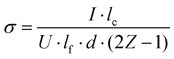
Interdigitated contacts were first patterned on as-grown tantalum nitride films by photolithography. For this, a layer of inversion image photoresist (AZ 5214E, MicroChemicals) was spin-coated onto the clean sample surface. After light exposure through a patterned photomask and subsequent development, e-beam evaporation was used to deposit consecutively 20 nm Ti and 80 nm Au. The remaining photoresist was then removed by acetone. Each contact consisted of thirteen 3.86 mm-long strips, with a minimum distance between the contacts of 60 μm.The in-plane electrical conductivity can be calculated via the slope of the current–voltage line with the following formula:
The photoconductivity was measured using a halogen lamp (MLC-150C, Motic) with a 3500 K color temperature, with a 15 min settling time before each measurement. The temperature dependence of the electrical conductivity was examined between 190–330 K, from low to high set temperature points, in a home-built setup.
Photoelectrochemical measurement
The test was conducted using an AM 1.5G solar simulator (HAL-320, Asahi Spectra) in a three-electrode configuration. A Ta2N3(O) thin film on a degenerately doped Si(100) substrate and a Pt wire served as the working and counter electrode, respectively, while a Ag/AgCl electrode immersed in 3 M KCl solution was used as the reference electrode. The pH 9.35 buffer solution consisted of 0.1 M H3BO3 and 0.05 M NaOH, and the addition of 0.1 M K4Fe(CN)6 served as a sacrificial hole acceptor. Current–potential characteristics were recorded with a potentiostat (SP-150, Bio-Logic).First principles calculations
Calculations were performed with VASP 5.4.449 and the plane-augmented wave method and pseudopotentials matching the Materials Project46 standard set with plane-wave cut-off of 520 eV and k-point reciprocal density of 64 k-points per inverse Å3 relaxations and 100 k-point reciprocal per Å3 for total energy calculations. To fully reproduce these calculations, please consult the workflows defined in the atomate50 and pymatgen43 code, specifically the “MPRelaxSet”, “MPStaticSet”, and “MPHSEBSSet” classes.For the electronic structure calculations, a crystal structure of bixbyite Ta2N3 and the same structure with interstitial oxygen atoms added for the Ta2N3O phase, were first relaxed with the PBEsol energy functional,36 and then the electronic structure was calculated using the HSE06 functional41 known to predict reasonably accurate band gaps in semiconductors to within a few tenths of eV.
For the phase diagram, calculations, similar geometry optimizations and total energy calculations were performed, except using the PBE energy functional51 to retain compatibility with existing Materials Project data. Alternative functionals were also explored for the Ta–N phase including the SCAN energy functional with differences in total energy of the order of 2 meV per atom, suggesting the PBE is sufficient for characterization of phase stability in this system.
Conflicts of interest
There are no conflicts to declare.Acknowledgements
This project has received funding from the European Research Council (ERC) under the European Union's Horizon 2020 research and innovation programme (grant agreement No. 864234). J. E. acknowledges funding by the Deutsche Forschungsgemeinschaft (DFG, German Research Foundation) – 428591260. M. K. H. acknowledges support by the U.S. Department of Energy, Office of Science, Office of Basic Energy Sciences, Materials Sciences and Engineering Division under Contract No. DE-AC02-05-CH11231 (Materials Project program KC23MP). M. K. H. acknowledges Matthew McDermott's work on pymatgen and its recently improved phase diagram plotting capabilities.References
- F. A. Ponce and D. P. Bour, Nature, 1997, 386, 351–359 CrossRef CAS.
- M. Asif Khan, A. Bhattarai, J. N. Kuznia and D. T. Olson, Appl. Phys. Lett., 1993, 63, 1214–1215 CrossRef.
- Y. Feng, E. Witkoske, E. S. Bell, Y. Wang, A. Tzempelikos, I. T. Ferguson and N. Lu, ES Mater. Manuf., 2018, 1, 13–20 Search PubMed.
- S. Yamanaka, Annu. Rev. Mater. Sci., 2000, 30, 53–82 CrossRef CAS.
- S. Chu, S. Vanka, Y. Wang, J. Gim, Y. Wang, Y.-H. Ra, R. Hovden, H. Guo, I. Shih and Z. Mi, ACS Energy Lett., 2018, 3, 307–314 CrossRef CAS.
- T. Higashi, H. Nishiyama, Y. Suzuki, Y. Sasaki, T. Hisatomi, M. Katayama, T. Minegishi, K. Seki, T. Yamada and K. Domen, Angew. Chem., Int. Ed., 2019, 58, 2300–2304 CrossRef CAS PubMed.
- J. Fu, F. Wang, Y. Xiao, Y. Yao, C. Feng, L. Chang, C.-M. Jiang, V. F. Kunzelmann, Z. M. Wang, A. O. Govorov, I. D. Sharp and Y. Li, ACS Catal., 2020, 10, 10316–10324 CrossRef CAS.
- W. Sun, S. T. Dacek, S. P. Ong, G. Hautier, A. Jain, W. D. Richards, A. C. Gamst, K. A. Persson and G. Ceder, Sci. Adv., 2016, 2, e1600225 CrossRef PubMed.
- P. Patsalas, N. Kalfagiannis, S. Kassavetis, G. Abadias, D. V. Bellas, C. Lekka and E. Lidorikis, Mater. Sci. Eng., R, 2018, 123, 1–55 CrossRef.
- M. Xu, S. Wang, G. Yin, J. Li, Y. Zheng, L. Chen and Y. Jia, Appl. Phys. Lett., 2006, 89, 151908 CrossRef.
- W. Sun, C. J. Bartel, E. Arca, S. R. Bauers, B. Matthews, B. Orvañanos, B. R. Chen, M. F. Toney, L. T. Schelhas, W. Tumas, J. Tate, A. Zakutayev, S. Lany, A. M. Holder and G. Ceder, Nat. Mater., 2019, 18, 732–739 CrossRef CAS PubMed.
- S. R. Bauers, A. Holder, W. Sun, C. L. Melamed, R. Woods-Robinson, J. Mangum, J. Perkins, W. Tumas, B. Gorman, A. Tamboli, G. Ceder, S. Lany and A. Zakutayev, Proc. Natl. Acad. Sci. U. S. A., 2019, 116, 14829–14834 CrossRef CAS PubMed.
- Y. Li, T. Takata, D. Cha, K. Takanabe, T. Minegishi, J. Kubota and K. Domen, Adv. Mater., 2013, 25, 125–131 CrossRef CAS PubMed.
- W. Sun, A. Holder, B. Orvañanos, E. Arca, A. Zakutayev, S. Lany and G. Ceder, Chem. Mater., 2017, 29, 6936–6946 CrossRef CAS.
- E. Bailey, N. M. T. Ray, A. L. Hector, P. Crozier, W. T. Petuskey and P. F. McMillan, Materials, 2011, 4, 1747–1762 CrossRef CAS PubMed.
- T. Taniguchi, D. Dzivenko, R. Riedel, T. Chauveau and A. Zerr, Ceram. Int., 2019, 45, 20028–20032 CrossRef CAS.
- A. Y. Ganin, L. Kienle and G. V. Vajenine, Eur. J. Inorg. Chem., 2004, 3233–3239 CrossRef CAS.
- C. Stampfl and A. J. Freeman, Phys. Rev. B: Condens. Matter Mater. Phys., 2005, 71, 024111 CrossRef.
- K. Salamon, N. Radić, I. Bogdanović Radović and M. Očko, J. Phys. D: Appl. Phys., 2016, 49, 195301 CrossRef.
- Y. He, P. Ma, S. Zhu, M. Liu, Q. Dong, J. Espano, X. Yao and D. Wang, Joule, 2017, 1, 831–842 CrossRef CAS.
- M. Xiao, B. Luo, M. Lyu, S. Wang and L. Wang, Adv. Energy Mater., 2018, 8, 1701605 CrossRef.
- D.-H. Lin and K.-S. Chang, J. Appl. Phys., 2016, 120, 075303 CrossRef.
- H. Hajibabaei, D. J. Little, A. Pandey, D. Wang, Z. Mi and T. W. Hamann, ACS Appl. Mater. Interfaces, 2019, 11, 15457–15466 CrossRef CAS PubMed.
- M. Rudolph, I. Vickridge, E. Foy, J. Alvarez, J.-P. Kleider, D. Stanescu, H. Magnan, N. Herlin-Boime, B. Bouchet-Fabre, T. Minea and M.-C. Hugon, Thin Solid Films, 2019, 685, 204–209 CrossRef CAS.
- C. Stampfl and A. J. Freeman, Phys. Rev. B: Condens. Matter Mater. Phys., 2003, 67, 064108 CrossRef.
- L. E. Conroy and A. N. Christensen, J. Solid State Chem., 1977, 20, 205–207 CrossRef CAS.
- H. J. Coyne and R. N. Tauber, J. Appl. Phys., 1968, 39, 5585–5593 CrossRef CAS.
- K. Salamon, M. Očko, N. Radić, I. Bogdanović Radović, V. Despoja and S. Bernstorff, J. Alloys Compd., 2016, 682, 98–106 CrossRef CAS.
- A. Zerr, G. Miehe, J. Li, D. A. Dzivenko, V. K. Bulatov, H. Höfer, N. Boifan-Casanova, M. Fialin, G. Brey, T. Watanabe and M. Yoshimura, Adv. Funct. Mater., 2009, 19, 2282–2288 CrossRef CAS.
- C. Jiang, Z. Lin and Y. Zhao, Phys. Rev. Lett., 2009, 103, 30–33 Search PubMed.
- R. J. Gaboriaud, F. Paumier and B. Lacroix, Thin Solid Films, 2016, 601, 84–88 CrossRef CAS.
- A. K. Nayak, S. Lee, Y. Sohn and D. Pradhan, Nanotechnology, 2015, 26, 485601 CrossRef PubMed.
- Y. Hu, Z. Long, K. Liu and J. Liu, Mater. Lett., 2016, 178, 124–127 CrossRef CAS.
- A. N. Fioretti, C. P. Schwartz, J. Vinson, D. Nordlund, D. Prendergast, A. C. Tamboli, C. M. Caskey, F. Tuomisto, F. Linez, S. T. Christensen, E. S. Toberer, S. Lany and A. Zakutayev, J. Appl. Phys., 2016, 119, 181508 CrossRef PubMed.
- C. M. Caskey, J. A. Seabold, V. Stevanović, M. Ma, W. A. Smith, D. S. Ginley, N. R. Neale, R. M. Richards, S. Lany and A. Zakutayev, J. Mater. Chem. C, 2015, 3, 1389–1396 RSC.
- J. P. Perdew, A. Ruzsinszky, G. I. Csonka, O. A. Vydrov, G. E. Scuseria, L. A. Constantin, X. Zhou and K. Burke, Phys. Rev. Lett., 2008, 100, 136406 CrossRef PubMed.
- I. Narkeviciute and T. F. Jaramillo, Sol. RRL, 2017, 1, 1700121 CrossRef.
- S. J. Henderson and A. L. Hector, J. Solid State Chem., 2006, 179, 3518–3524 CrossRef CAS.
- G. Fan, X. Wang, H. Fu, J. Feng, Z. Li and Z. Zou, Phys. Rev. Mater., 2017, 1, 035403 CrossRef.
- X. P. Du, Y. X. Wang and V. C. Lo, J. Phys. Chem. C, 2011, 115, 3129–3135 CrossRef CAS.
- A. V. Krukau, O. A. Vydrov, A. F. Izmaylov and G. E. Scuseria, J. Chem. Phys., 2006, 125, 224106 CrossRef PubMed.
- A. M. Ganose, A. J. Jackson and D. O. Scanlon, J. Open Source Softw., 2018, 3, 717 CrossRef.
- S. P. Ong, W. D. Richards, A. Jain, G. Hautier, M. Kocher, S. Cholia, D. Gunter, V. L. Chevrier, K. A. Persson and G. Ceder, Comput. Mater. Sci., 2013, 68, 314–319 CrossRef CAS.
- J. Pan, J. Cordell, G. J. Tucker, A. C. Tamboli, A. Zakutayev and S. Lany, Adv. Mater., 2019, 31, 1–8 Search PubMed.
- J. Kim, S. R. Bauers, I. S. Khan, J. Perkins, B. I. Park, K. R. Talley, D. Kim, A. Zakutayev and B. Shin, J. Mater. Chem. A, 2020, 8, 9364–9372 RSC.
- A. Jain, J. Montoya, S. Dwaraknath, N. E. R. Zimmermann, J. Dagdelen, M. Horton, P. Huck, D. Winston, S. Cholia, S. P. Ong and K. Persson, Handbook of Materials Modeling, Springer International Publishing, Cham, 2018, pp. 1–34 Search PubMed.
- M. Aykol, S. S. Dwaraknath, W. Sun and K. A. Persson, Sci. Adv., 2018, 4, eaaq0148 CrossRef PubMed.
- H. F. W. Dekkers, L.-Å. Ragnarsson, T. Schram and N. Horiguchi, J. Appl. Phys., 2018, 124, 165307 CrossRef.
- G. Kresse and J. Furthmüller, Comput. Mater. Sci., 1996, 6, 15–50 CrossRef CAS.
- K. Mathew, J. H. Montoya, A. Faghaninia, S. Dwarakanath, M. Aykol, H. Tang, I. Chu, T. Smidt, B. Bocklund, M. Horton, J. Dagdelen, B. Wood, Z.-K. Liu, J. Neaton, S. P. Ong, K. Persson and A. Jain, Comput. Mater. Sci., 2017, 139, 140–152 CrossRef.
- J. P. Perdew, K. Burke and M. Ernzerhof, Phys. Rev. Lett., 1998, 80, 891 CrossRef CAS.
Footnote |
| † Electronic supplementary information (ESI) available. See DOI: 10.1039/d1mh00017a |
| This journal is © The Royal Society of Chemistry 2021 |