
Infrared spectroscopy depth profiling of organic thin films†
Jinde
Yu
a,
Yifan
Xing
a,
Zichao
Shen
a,
Yuanwei
Zhu
a,
Dieter
Neher
 b,
Norbert
Koch
cd and
Guanghao
Lu
*a
b,
Norbert
Koch
cd and
Guanghao
Lu
*a
aFrontier Institute of Science and Technology and State Key Laboratory of Electrical Insulation and Power Equipment, Xi’an Jiaotong University, Xi’an, 710054, China. E-mail: guanghao.lu@xjtu.edu.cn
bInstitut für Physik und Astronomie, Universität Potsdam, Potsdam 14476, Germany
cInstitut für Physik & IRIS Adlershof, Humboldt-Universität zu Berlin, Berlin 12489, Germany
dHelmholtz-Zentrum Berlin für Materialien und Energie GmbH, Berlin 12489, Germany
First published on 11th February 2021
Abstract
Organic thin films are widely used in organic electronics and coatings. Such films often feature film-depth dependent variations of composition and optoelectronic properties. State-of-the-art depth profiling methods such as mass spectroscopy and photoelectron spectroscopy rely on non-intrinsic species (vaporized ions, etching-induced surface defects), which are chemically and functionally different from the original materials. Here we introduce an easily-accessible and generally applicable depth profiling method: film-depth-dependent infrared (FDD-IR) spectroscopy profilometry based on directly measuring the intrinsic material after incremental surface-selective etching by a soft plasma, to study the material variations along the surface-normal direction. This depth profiling uses characteristic vibrational signatures of the involved compounds, and can be used for both conjugated and non-conjugated, neutral and ionic materials. A film-depth resolution of one nanometer is achieved. We demonstrate the application of this method for investigation of device-relevant thin films, including organic field-effect transistors and organic photovoltaic cells, as well as ionized dopant distributions in doped semiconductors.
New conceptsThis work introduces an infrared spectroscopy profilometry, to study the composition distribution of organic thin films along the film depth direction. Infrared spectra allow reliable identification of species with high resolution. Three model electronic organic films, including conducting polymer:insulating polymer (for transistors), donor:acceptor (for photovoltaic cells) bulk heterojunctions and doped organic semiconductors, are used as examples to demonstrate that this depth profiling methodology can indeed be generally applied for organic thin films. This approach provides insights into conjugated and non-conjugated (and mixed) organic thin films, neutral and ionic materials, all based on equipment and methodology easily accessible in most laboratories worldwide. |
Introduction
Organic thin films are widely used in organic electronics, as well as for device encapsulation and packaging.1,2 During the deposition of the films, the complex interactions between substrate, organic components, and solvents often lead to variable vertical phase distribution along the film-depth,3,4 which can be reduced or enhanced by post-processing e.g. annealing. Therefore, for many organic thin films, the surface and bulk at different film-depth exhibit different properties, such as composition, crystallinity,5,6 crystallite orientation,7 as well as electronic and optical properties.8,9 These vertical variations significantly impact the performance of devices. For example, in thin film organic field-effect transistors (OFETs), charge injection, transport, and accumulation can take place at different film-depth.10,11 In organic photovoltaic (OPV) devices, where a donor:acceptor bulk heterojunction is the active layer,12–15 both photon harvesting and charge transport are film-depth dependent and thus the composition distribution profile along the surface-normal direction has a significant influence on the device performance. Another example where vertical composition gradient plays an important role is doped organic semiconductors (OSCs) films. Depending on dopant and OSC interactions, as well as processing conditions, phase separation between dopant and OSC may occur16,17 and result in non-uniform ionized dopant distribution along the surface-normal direction, which strongly impacts the functionality of such films. Consequently, being able to reliably determine composition and property variations as function of film-depth is key for advanced device design.Depth profiling methods have attracted increasing interest to determine film-depth-dependent variations. For instance, incremental etching of thin films with high-energy ions is used for depth profiling in combination with secondary ion mass spectroscopy,18,19 X-ray photoelectron spectroscopy,20–22 and ultraviolet photoelectron spectroscopy.23 Such analysis techniques rely on either detecting the vaporized (etched) ionic species or probing the etched surface. However, the vaporized species and etched surface are usually chemically and functionally modified by the etching process compared to the pristine original material, which reduces the reliability and applicability of these methods. Moreover, the etching rate can significantly differ for different film components, so that the sample composition at the etched surface can significantly deviate from the actual composition before etching. Therefore, these surface analytical techniques are only applicable to a limited fraction of samples, and they are rather cost-intensive and not readily accessible in most laboratories. Therefore, a complementary method that does not face these mentioned challenges would boost studies of film-depth-dependent characteristics of organic thin films and enable to improve thin film engineering.
Recently, film-depth-dependent ultraviolet-visible (UV-Vis) absorption spectroscopy24–28 has been introduced and applied to several organic films. With this method, the desired information is derived from the light transmitted through the sample after incremental etching-steps, thus probing the entire remaining film, instead of just the surface. This method could partly resolve the limitations of surface analysis and provide insight into film properties in a depth-resolved manner, covering a wide thickness range from a few to hundreds of nanometers. However, non-conjugated organic materials are mostly wide-gap insulators and do not have notable UV-Vis absorption. Moreover, UV-Vis spectroscopy is based on electronic excitations, which are often coupled with molecular vibrations, and thus spectra can be rather broad. In addition, UV-Vis spectra also strongly depend on crystallinity, molecular orientation and conformation. Consequently, film-depth-dependent UV-Vis spectra usually contain multiple complex peaks with possibly ambiguous variation of profiles along the surface-normal direction, which thus induces a practically poor resolution in terms of both wavelength and film depth. These issues make analysis very challenging or imply a large error margin.
Compared to UV-Vis absorption, infrared light absorption, corresponding to molecular vibrational excitations, usually features much better defined peaks in the spectra. In fact, infrared light tomography has been used for medical,29 materials,30 and environmental31 applications. Also, infrared spectroscopy in conjunction with atomic force microscopy32 (AFM) is emerging as a microscopic analysis technique for in-plane mapping of organic blend films. However, because the wavelength of infrared light is on the order of a micrometer or longer, which is more than the typical organic film thickness on the order of 100 nm or less in organic electronics, the spatial resolution of infrared tomography is not sufficient for film-depth profilometry.
Taking the above considerations into account, we here introduce an infrared spectroscopy based profilometry, film-depth-dependent infrared (FDD-IR) spectroscopy, that uses the vibrational spectra distribution along the surface-normal direction in conjunction with soft plasma etching. This depth profiling method can be used for conjugated and non-conjugated organic materials, or for neutral molecules and ionized species, with sufficient wavelength resolution and depth resolution reaching around one nanometer. This work is organized by the following way. First, the method is introduced, verified and optimized by the use of a classic polythiophene semiconductor. Subsequently, the depth profiling method is applied to bilayers to confirm its validity. Afterwards, conducting polymer:insulating polymer (for OFETs) and donor:acceptor (for OPVs) bulk heterojunctions are used as examples to demonstrate the wide applications of this method. Finally, to extend the measurement capability of FDD-IR from neutral molecule materials to ion systems, a doped OSC film is used to investigate ionized dopant distributions along the film-depth direction.
Results and discussion
Principles of FDD-IR spectroscopy
The general measurement sequence for FDD-IR spectroscopy is illustrated in Fig. 1a. Part of the infrared light emitted by the source transmits through the film and substrate and is monitored by a detector. In the present studies calcium fluoride (CaF2) was used as substrate because it is transparent for infrared light in the range of 3500 cm−1–1000 cm−1. After acquisition of a spectrum the organic film is etched by low pressure glow plasma (soft plasma), and afterwards another spectrum from the etched film is recorded. The variation of the spectra during etching is thus used to extract the spectrum of the etched sublayer. This sequence is then accordingly repeated, to sequentially obtain the spectrum of each sublayer. Besides, it is recommended to implement suitable means to guarantee that the same location of film is measured in the process of collecting the FDD-IR spectra upon soft plasma etching back and forth, e.g., by using markers. A prerequisite for this approach is that we selectively etch the film surface gradually towards different film depth, keeping the properties of the remaining film unchanged. This can be achieved by optimized low pressure plasma etching, as demonstrated exemplarily here for poly(3-hexylthiophene) (P3HT), which is a prototypical conjugated polymer semiconductor for use in OFETs33 and OPV cells.34Fig. 1b compares the infrared spectra of P3HT films before and after treatment with low pressure (20 Pa, 2 min) argon plasma, high pressure (200 Pa, 2 min) argon plasma, and ultraviolet (UV) ozone (atmospheric pressure, 5 min) etching, respectively. After low pressure plasma treatment, the infrared spectrum of the etched P3HT film is virtually identical to that of the pristine one. In contrast, significant changes, in terms of both infrared (IR) intensity and peak positions, are observed after treatments by high pressure plasma and UV ozone, which indicates that the treated films comprise no longer only intact P3HT. Fig. 1c and d schematically show the different effects of glow discharge treatment (at low pressure) and filamentous discharge (at high pressure). At low pressure, surface-selective etching is realized via the interaction of plasma species and the organic material, and the etching is homogenous at the surface.35 Filamentous discharge, in contrast, etches the sample in-homogeneously and damages the material locally due to high energy and high density ion pulses. AFM (Fig. S1a–d, ESI†) revealed little changes of surface roughness by glow discharge plasma etching at low pressure, while both high pressure argon plasma and UV ozone etching significantly increased the surface roughness, in addition to damaging the material as seen from the IR spectra. In fact, it is known that filamentous discharge at high pressure may puncture the film and thus damage the material underneath the surface.36–38 Therefore, low pressure plasma etching is an ideal surface-selective etching technique suitable for FDD-IR spectroscopy, rendering the remaining film intact.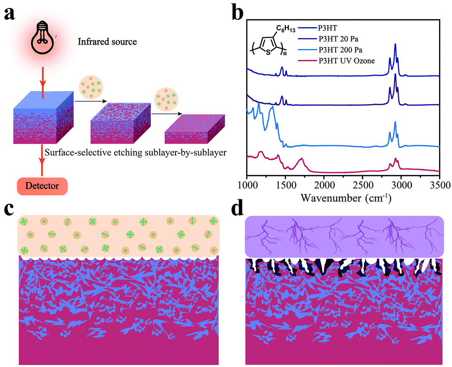 | ||
| Fig. 1 Schematic diagram of FDD-IR spectroscopy upon surface-selective etching method. (a) The red line represents the incident and transmitted infrared light of FDD-IR spectroscopy. The infrared absorption spectra of the organic thin films are measured during the surface-selective etching without the damage to the underneath materials. The FDD-IR spectra are extracted from the evolution of the transmission light intensity, and therefore measures the bulk materials rather than the etched surface. (b) The infrared spectra of pure P3HT films without or with treatment by argon plasma with different argon pressure and UV ozone, respectively. Low pressure glow plasma warrants effective etching for FDD-IR spectroscopy. (c and d) Schematic diagram of etching by glow discharge at low argon pressure (c, soft plasma) and filamentous discharging at high argon pressure (d). During the discharge, the microscopic filaments could ruin the organic materials and therefore should be carefully avoided for the FDD-IR measurements. | ||
Having established that low pressure plasma etching is suitable for our purpose, we demonstrate the capability of FDD-IR spectroscopy with respect to depth-profiling for representative examples pertaining to organic electronics in the following. Many organic materials exhibit dozens of vibrational peaks that may actually overlap spectrally, so that the investigation of blends of materials with diagnostic spectral features is more straightforward. For instance, carbonyl (C![[double bond, length as m-dash]](https://www.rsc.org/images/entities/char_e001.gif) O) and cyano (C
O) and cyano (C![[triple bond, length as m-dash]](https://www.rsc.org/images/entities/char_e002.gif) N) groups are two representative moieties in organic materials that provide for such a fingerprint. Three model blend systems used in OFET, OPV and doped OSCs applications were chosen, i.e., PMMA:PDPPDTT,39 PM6:Y640–42 and F4TCNQ:P3HT (for chemical structures see in Fig. 2). The IR-diagnostic groups are 2,5-(2-octyldodecyl)-3,6-diketopyrrolopyrrole (DPP),43 the ester group, the cyano group, benzo[1′,2′-c:4′,5′-c′]dithiophene-4,8-dione (BDD),44 and 1,1-dicyanomethylene-3-indanone (IC),45 and they are highlighted by color in Fig. 2.
N) groups are two representative moieties in organic materials that provide for such a fingerprint. Three model blend systems used in OFET, OPV and doped OSCs applications were chosen, i.e., PMMA:PDPPDTT,39 PM6:Y640–42 and F4TCNQ:P3HT (for chemical structures see in Fig. 2). The IR-diagnostic groups are 2,5-(2-octyldodecyl)-3,6-diketopyrrolopyrrole (DPP),43 the ester group, the cyano group, benzo[1′,2′-c:4′,5′-c′]dithiophene-4,8-dione (BDD),44 and 1,1-dicyanomethylene-3-indanone (IC),45 and they are highlighted by color in Fig. 2.
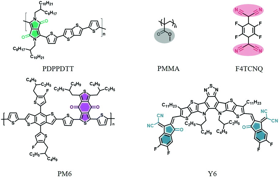 | ||
| Fig. 2 The model materials studied for FDD-IR: PDPPDTT, PMMA, F4TCNQ, PM6 and Y6. The highlighted chemical groups containing CO or CN bonds contribute to strong vibronic absorptions in the mid-infrared region. | ||
FDD-IR spectroscopy of PMMA/PDPPDTT bilayer and blend films
As benchmark, a bilayer structure of PMMA (20 nm thick)/PDPPDTT (30 nm), prepared by orthogonal solvent casting, was used to demonstrate the capability of depth profiling. Fig. 3a shows the evolution of FDD-IR spectra of the PMMA/PDPPDTT bilayer film as function of low pressure plasma etching time, at each step for 45 s. Overall, all peaks in the 3500–1000 cm−1 region gradually disappear with increasing etching time. In more detail, the intensity of the peak at 1729 cm−1 (CO of PMMA) gradually decreases towards zero, and only from this point onwards the intensity of the peak at 1666 cm−1 (CO of PDPPDTT) starts to drop until the bilayer film is completely etched. The peak positions and line shapes remain unchanged throughout, which already proves the feasibility and practicability of depth profiling by FDD-IR spectroscopy. To further examine the depth profiling method and expand its applications, PMMA:PDPPDTT blend films are utilized to study the composition distribution along the surface-normal direction. Fig. 3b and c show the evolution of FDD-IR spectra of PMMA![[thin space (1/6-em)]](https://www.rsc.org/images/entities/char_2009.gif) :PDPPDTT (weight ratio 4:1) and PMMA:PDPPDTT (weight ratio 1:1) blend films during soft plasma etching, respectively. All these blend films are also etched by low pressure argon plasma with etching time 12 s for each step. Again, all infrared peaks in the 3500–1000 cm−1 region gradually decrease in intensity with increased etching time. Owing to relatively fewer carbonyl groups per unit mass of PDPPDTT compared with that of PMMA, and the lower content of PDPPDTT in the PMMA:PDPPDTT (4:1) blend film, the intensity of PDPPDTT (CO) at 1666 cm−1 is comparatively weak. Thus, another diagnostic infrared double-peak (1496 cm−1 to 1610 cm−1) (CC) representative of PDPPDTT is used for further analysis and shown in detail on the right side of Fig. 3b and c. Both the double-peak representing PDPPDTT and the carbonyl peak (PMMA) at 1729 cm−1 are used in the following for calculating the composition distribution along the surface-normal direction.
:PDPPDTT (weight ratio 4:1) and PMMA:PDPPDTT (weight ratio 1:1) blend films during soft plasma etching, respectively. All these blend films are also etched by low pressure argon plasma with etching time 12 s for each step. Again, all infrared peaks in the 3500–1000 cm−1 region gradually decrease in intensity with increased etching time. Owing to relatively fewer carbonyl groups per unit mass of PDPPDTT compared with that of PMMA, and the lower content of PDPPDTT in the PMMA:PDPPDTT (4:1) blend film, the intensity of PDPPDTT (CO) at 1666 cm−1 is comparatively weak. Thus, another diagnostic infrared double-peak (1496 cm−1 to 1610 cm−1) (CC) representative of PDPPDTT is used for further analysis and shown in detail on the right side of Fig. 3b and c. Both the double-peak representing PDPPDTT and the carbonyl peak (PMMA) at 1729 cm−1 are used in the following for calculating the composition distribution along the surface-normal direction.
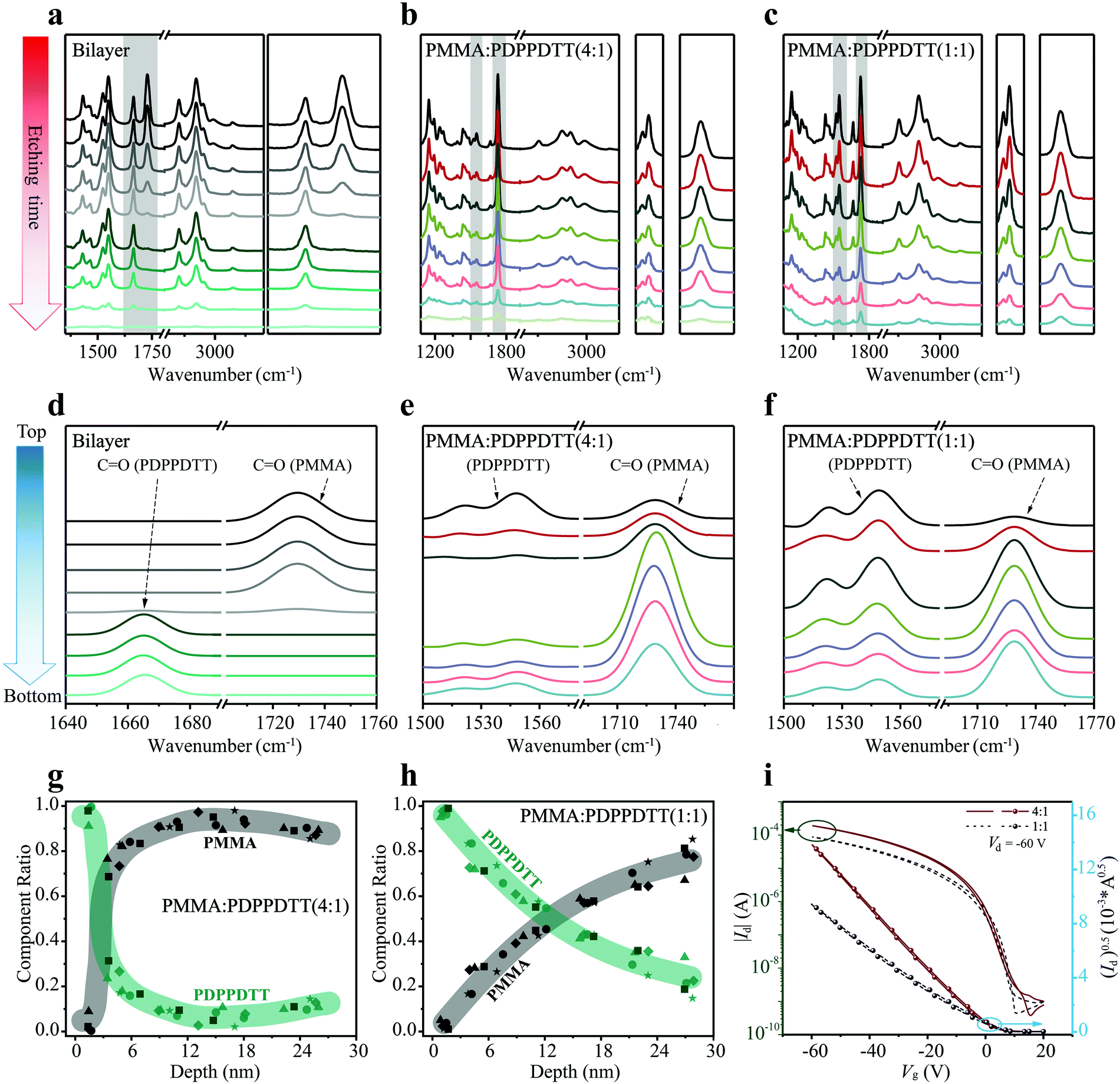 | ||
| Fig. 3 Applications of FDD-IR in semiconductor:insulator polymer blends for OFETs. (a–c) Depth profiling of PMMA/PDPPDTT bilayer film (a), PMMA:PDPPDTT (4:1) (b) and PMMA:PDPPDTT (1:1) (c) blend films. The peaks in the shaded region, which represent the characteristic functional groups of different materials, are re-scaled in the right side of (a), (b) and (c), respectively. (d–f) The numerically fitted FDD-IR spectroscopy of PMMA/PDPPDTT bilayer film (d), PMMA:PDPPDTT (4:1) (e) and PMMA:PDPPDTT (1:1) (f) blend films. The FDD-IR spectra at different film-depth are fitted by Gaussian distribution and vertically re-arranged from the top to the bottom surface of organic films. (g and h) Composition distribution profiles at different film-depths. The darker square symbols are numerically extracted from (b and c), while other shaped symbols are obtained from the identical experimental measurements of other four samples. The colored regions are guides to eyes. (i) OFET transfer characteristics of PMMA:PDPPDTT (4:1) and PMMA:PDPPDTT (1:1) blend films. | ||
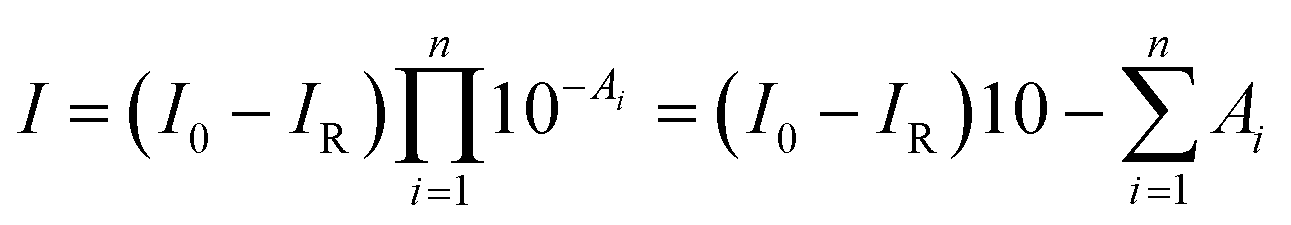
According to the Lambert–Beer law, the absorbance of the film (A) is defined as A = −log[I/(I0 − IR)], where I, I0, and IR are the intensity of transmitted, incident, and reflected infrared light, respectively. IR can be ignored in the infrared measurements. We assumed that the film is composed of n sublayers, and each sublayer is located at different film-depth. Therefore, the intensity of infrared light after passing through n sublayers is obtained as
 | (1) |
Fig. 3d–f show the FDD-IR spectra after Gaussian fitting for the PMMA/PDPPDTT bilayer film and PMMA:PDPPDTT (4:1 and 1:1) blend films, which are originally extracted from Fig. 3a–c by the following method. At first, all characteristic peaks are fitted by a Gaussian distribution, and the detailed fitting process is shown in the Fig. S2a–c (ESI†). Then, the numerically fitted FDD-IR spectra are obtained from Lambert–Beer law. All fitted FDD-IR spectra are arranged separately along the blue arrow (Fig. 3d–f), each spectrum corresponding to a sublayer inside the organic thin films. In principle, all organic films discussed here could be divided into more sublayers through incremental soft plasma etching. However, to avoid experimental errors, all organic films reasonably were chosen to consist of 6 to 8 sublayers, and the number of sublayers corresponds to the number of etching steps. In Fig. 3d, the peaks of PMMA (CO) only exist in the top four sublayers, while the peaks of PDPPDTT (CO) are present only in the bottom four sublayers, i.e., the interface is as sharp as expected. For fitting the FDD-IR spectra of PMMA:PDPPDTT (4:1) blend film in Fig. 3e, the film is assumed to consist of seven sublayers, in which the double-peaks (CC) of PDPPDTT mainly present in the first and last sublayers and the peaks of PMMA (CO) appear in all sublayers. As for the FDD-IR fitting of the PMMA:PDPPDTT (1:1) blend film in the Fig. 3f, the film is also composed of seven sublayers, in which the intensity of the double-peak gradually decreases from top to bottom. The peak of PMMA (CO) reaches its maximum intensity below the upper two sublayers. The Lambert–Beer law model of infrared spectra explained above enable obtaining the composition distribution profiles across the film thickness as shown in Fig. 3g and h. The zero (0 nm) in Fig. 3g and h corresponds to the top surface of the blend films and the thicknesses of the two blend films are both 30 nm. In Fig. 3g and h, the different symbols correspond to measurements done on five nominally identically prepared films, to improve the reliability of the results. It is observed that PDPPDTT is primarily enriched at the surface (sublayer thickness 5 nm) of the PMMA:PDPPDTT (4:1) blend film, while its content sharply decreases towards the bottom (Fig. 3g), showing a well-defined vertical phase separation. For the PMMA:PDPPDTT (1:1) blend film, the composition distribution (Fig. 3h) shows a different scenario from that of the PMMA:PDPPDTT (4:1) blend. The content of PDPPDTT gradually decrease from top to bottom surface of the blend film. Although the composition distributions in the two cases are different, the surface of both blend films is covered by a ca. 5 nm thick semiconducting PDPPDTT sublayer. Additionally, the thicknesses of original blend films before etching were measured by a step profiler, while the thicknesses of etched blend films were obtained by the variation of the IR spectra intensity, as explained in the Experimental section.
Charge transport properties are key for the performance of OFETs, and they are strongly influenced by the composition distribution of the blend films along the surface-normal direction. Transfer curves and output curves of bottom-gate top-contact OFETs made with PMMA:PDPPDTT blend films are shown in Fig. 3i and Fig. S3 (ESI†). The overall performance of the PMMA:PDPPDTT (4:1) blend film transistor is better than that made with the PMMA:PDPPDTT (1:1) blend, although the former has a higher insulator content. For the PMMA:PDPPDTT (4:1) blend film transistor, the mobility, on/off ratio, and threshold voltage (Vth), are 1.09 cm2 V−1 s−1, 105, and 0 V, respectively. For the PMMA:PDPPDTT (1:1) blend film transistor, these values are 0.51 cm2 V−1 s−1, <105, and 5 V, respectively. As seen from Fig. 3g and h, PDPPDTT accumulates at the top of PMMA:PDPPDTT (4:1) blend film, forming a continuous and uniform semiconducting sublayer, which enhances charge transport and leads to a higher field-effect mobility compared to PMMA:PDPPDTT (1:1) transistors. The uniformly distributed insulating PMMA without PDPPDTT ensures high electrical resistance of the dielectric sublayer, which is beneficial for the on/off characteristics. Actually, many polymer semiconductor:insulator blends with similar vertical phase separation have been widely used for OFETs, which have shown superior performance if the morphology is optimized, as compared with the pure conjugated polymers.46–48 The inert PMMA insulator matrix not only improves the crystalline ordering of PDPPDTT, but also shields the charge traps on the SiO2 surface.
FDD-IR spectroscopy for OPV cells
Subsequently, we turn to the application of FDD-IR for OPV investigations. To confirm the reliability of the FDD-IR method, an ideal bilayer was employed firstly. A donor/acceptor bilayer film of PM6 (200 nm)/Y6 (80 nm) was fabricated by a transfer method and the evolution of FDD-IR spectra as function of etching time (6 min for each step) is shown in Fig. 4a. The peak at 1647 cm−1 (CO), characteristic of PM6, decreases to zero during the incremental etching, followed by the decrease of the Y6 fingerprint-peaks at 1697 cm−1 (CO) and 2216 cm−1 (CN). Additionally, two different blend films (as-cast and solvent-annealed (over annealed) PM6:Y6) were investigated to further validate our methodology. Fig. 4b and c shows the evolution of FDD-IR spectra of these blend films as a function of etching time, each step corresponding to 2.5 min. All infrared peaks in the range 3500–1000 cm−1 gradually drop in intensity with increasing etching time, without any apparent peak-shift. The peaks in the shaded region, which represent the characteristic vibrations of PM6 and Y6, are shown separately on the right side of Fig. 4a–c. Also here, Gaussian fitting and sublayer calculations were performed in analogy to the blends used for OFETs, and the results are shown in Fig. 4d–f. Fig. 4d shows that the bilayer film is made up of eight sublayers, in which the peaks of PM6 (CO) show up in the top four sublayers and the peaks of Y6 (CO) in the bottom three sublayers. As for the fitting of FDD-IR for as-cast and solvent-annealed PM6:Y6 blend films in Fig. 4e and f, the leftmost peak is characteristic of PM6, while other two column peaks represent the carbonyl and cyano vibrations of Y6. For clarity, the as-cast PM6:Y6 (Fig. 4e) blend film is divided into five sublayers. Each sublayer has different PM6 (CO) and Y6 (CO) absorption intensity, implying a different composition in each sublayer. The solvent-annealed PM6:Y6 blend film (Fig. 4f) is also modeled as being composed of five sublayers, in which the peak intensity of Y6 (CO and CN) is very weak in the first sublayer, indicating an enrichment of PM6 on the top surface of the film. The detailed fitting process of all characteristic peaks for these samples is shown in the Fig. S2d–f (ESI†). In addition, due to the weak intensity of the infrared peak at the bottom of Fig. 4c, it is not useful to numerically fit this infrared peak, as also confirmed in the Fig. S2f (ESI†). The fifth fitting infrared peak at the bottom of Fig. 4f is corresponding to the penultimate infrared peak in Fig. 4c. Consequently, the fifth fitting infrared peak at the bottom of Fig. 4f is the sum of the rightmost two sets of data points (depth of about 75 nm and 95 nm) in Fig. 4h. Nevertheless, all component distribution results are extracted from the original data rather than the fitted data.
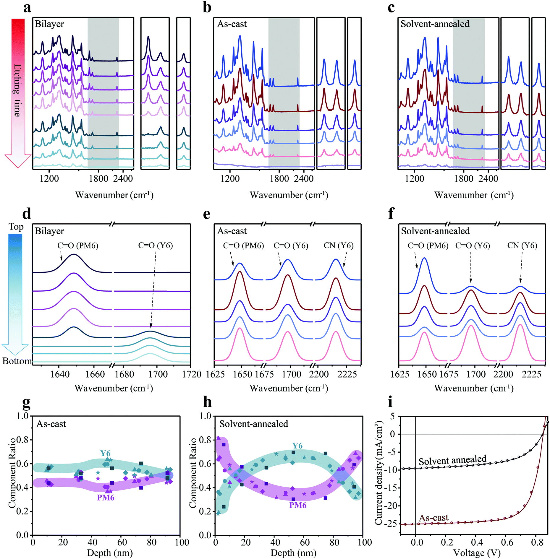 | ||
| Fig. 4 Applications of FDD-IR in organic donor:acceptor bulk heterojunction for OPVs. (a–c) Depth profiling of PM6/Y6 bilayer film (a), as-cast (b) and solvent-annealed (c) PM6:Y6 blend films. The peaks in the shaded region, which represent the characteristic functional groups of different materials, are re-scaled in the right side of (a), (b) and (c), respectively. (d–f) The numerically fitted FDD-IR spectroscopy of PM6/Y6 bilayer film (d), as-cast (e) and solvent-annealed (f) PM6:Y6 blend films. The FDD-IR spectra were fitted by Gaussian distribution. (g and h) Composition distribution profiles at different film-depths. The darker square symbols are numerically extracted from (b and c), while other shaped symbols are obtained from the identical experimental measurements of other four samples. The colored regions are guides to eyes. (i) J–V curves of as-cast and solvent-annealed PM6:Y6 photovoltaic devices measured under AM 1.5G illumination. | ||
The vertical composition distributions of as-cast and solvent-annealed PM6:Y6 blend films are shown in Fig. 4g and h. The thicknesses of the two kinds of blend films are both 100 nm, which was also measured by a step profiler, and the thickness of films during etching was obtained by the same spectroscopic way as explained above for PMMA:PDPPDTT blend films. It is noted that the peaks of PM6 at 1647 cm−1 (CO) and the peaks of Y6 at 2216 cm−1 (CN) were utilized for composition calculations. For the as-cast blend film, the content of PM6 and Y6 along the surface-normal direction varies only slightly, demonstrating a good miscibility of PM6 and Y6 throughout the blend film. In contrast, solvent annealing leads to an enrichment of PM6 at the top and bottom of the film, while Y6 is mainly located in the middle of the blend film, corresponding to a sandwich-like morphology with an apparent vertical phase separation.
It is apparent that the power conversion efficiency of OPV cells made with the as-cast blend film (up to 15%) is much higher than that of the solvent-annealed one (∼4.5%) (Fig. 4i). After solvent annealing for a long time, the short-circuit current density (Jsc) and fill factor sharply drop, leading to the huge loss in power conversion efficiency. Jsc decreases from 25.03 mA cm−2 of the as-cast film to 9.51 mA cm−2 of the solvent-annealed film, while fill factor decreases from 70% to 56%, although the open-circuit voltage (Voc) of the two OPV cells is almost identical. The evolution of FDD-IR spectroscopy profiles (Fig. 4b and c) and composition distribution profiles (Fig. 4g and h) demonstrate that large vertical phase separation due to intensified annealing results in the remarkable decrease of device performance. In fact, the optimal solvent annealing time for active layers is often less than one minute in sufficient solvent atmosphere. It has been shown that solvent annealing times of two minutes or more (intensified solvent annealing) cause device performance degradation.49
FDD-IR spectroscopy on doped OSCs
FDD-IR spectroscopy can be applied to not only to films with charge-neutral components, but also with ionic species. In the following, we exemplify this to investigate the dopant-ion distribution along the film-depth for doped OSCs. Two kinds of dopant:OSC films were investigated: the p-type dopant F4TCNQ was spin-coated onto neat P3HT films (thickness 80 nm) either from acetonitrile (MeCN) or from tetrahydrofuran:dichloromethane (with a volume ratio 3:1). The evolution of corresponding FDD-IR spectra is shown in Fig. 5a and b. The peak at 2227 cm−1 (CN) is assigned to neutral F4TCNQ and the peaks from 2100 cm−1 to 2218 cm−1 (CN) belong to negatively charged F4TCNQ (F4TCNQ−), which gives rise to the doping effect. The absorption of P3HT is in the range of 2800–3000 cm−1. All infrared peaks in the range 3100–1000 cm−1 gradually drop in intensity with incremental etching time. The peaks in the colored shaded region, which are the cyano-group stretch modes of F4TCNQ− and F4TCNQ, are shown separately on the right side of Fig. 5a and b. Notably, charged and neutral F4TCNQ coexist through the entire films along the surface-normal direction. Next, the composition distribution of (P3HT + P3HT+) over (F4TCNQ + F4TCNQ−) was numerically extracted and is shown in Fig. 5c and d. For both films, the amount of (P3HT + P3HT+) gradually increases from surface to substrate. In contrast, the amount of (F4TCNQ + F4TCNQ−) shows the opposite trend. For the sample where F4TCNQ was cast from MeCN, the content of (F4TCNQ + F4TCNQ−) is high only in the depth location 0–40 nm below the top surface. In contrast, the (F4TCNQ + F4TCNQ−) content is high even at the depth 60 nm below the top surface, and a plateau appears between 40 nm and 60 nm film-depths in the F4TCNQ:P3HT film made with the dopant from the co-solvent, demonstrating a more apparent swelling behavior compared to that from MeCN. It should be additionally noted that the thicknesses of all doped OSC films by the soft plasma etching were measured by a step profiler after each etching.
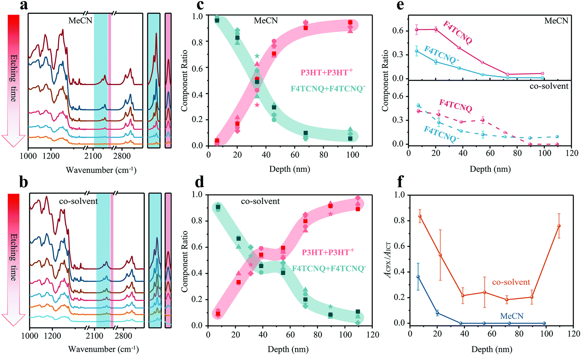 | ||
| Fig. 5 Applications of FDD-IR in doped OSCs. (a and b) Depth profiling of F4TCNQ:P3HT films fabricated upon sequentially processed method. F4TCNQ was spin-coated from MeCN (a) or co-solvent (b) onto pre-coated P3HT layer. The peaks in the shaded region, which represent the cyano-group of different charged states, are re-scaled in the right side of (a) and (b), respectively. (c and d) Composition distribution profiles of (P3HT + P3HT+) and (F4TCNQ + F4TCNQ−) at different film-depths. The darker square symbols are numerically extracted from (a and b), while other shaped symbols are obtained from the identical experimental measurements of other four samples. The colored regions are guides to eyes. (e) The content of F4TCNQ or F4TCNQ− at different film-depths in doped films derived from (a) and (b). (f) ACPX/AICT ratio numerically extracted from (a) and (b). | ||
The content of F4TCNQ and F4TCNQ− at different film-depth in the doped OSC films was numerically extracted from FDD-IR (Fig. 5e). The initial doping degree, i.e., the fraction of dopant anions compared to the overall number of dopants added, can be calculated in the Fig. S4 (ESI†). The amount of F4TCNQ and F4TCNQ− decreases from the top to the bottom surface of the film, in agreement with the component distribution discussed above (Fig. 5c and d). As for the F4TCNQ:P3HT (MeCN) film, the concentration of F4TCNQ and F4TCNQ− drop rapidly within 40 nm from the surface, while the content of F4TCNQ and F4TCNQ− decreases more gently in F4TCNQ:P3HT (co-solvent) film, especially for the neutral F4TCNQ fraction. Actually, P3HT film deposited from solution usually has a vertical phase segregation, and the film top surface typically features higher crystallinity and lower ionization energy.50 Therefore, after the inclusion of dopant F4TCNQ during film swelling, the doping concentration at the top surface is higher than the bulk.
A more detailed data analysis is done to retrieve the relative fraction of integer charge transfer (ICT) and charge transfer complex (CPX) states, both of which can occur upon doping P3HT with F4TCNQ.7,51,52 All F4TCNQ− peaks (CN) from 2100 cm−1 to 2218 cm−1 are analyzed in detail (Fig. S5 andS6, ESI†), where the peak at 2203 cm−1 is considered as the characteristic absorption of the CPX state, while those at 2169, 2179, 2186 and 2194 cm−1 indicate the ICT states. The absorbance ratio at 2203 cm−1 and 2186 cm−1, noted as ACPX/AICT, is utilized to visualize the distribution of the two different charge transfer states along the surface-normal direction. Fig. 5f shows that CPX states mainly exists within 20 nm of the top surface, and ICT states dominate the whole film made with the dopant coated from MeCN. In contrast, both CPX and ICT states co-exist throughout the film doped from co-solvent. Besides, the ratio of CPX to ICT is at a higher level both at the surface and bottom of such films.
As shown above, quantitative vertical diffusion and component distribution in doped OSCs can be reconstructed in great detail. For these films, during the sequential deposition process, the F4TCNQ dopants deeply diffuse into the host P3HT, depending on the chosen conditions. The electrical conductivity of the films made with MeCN is 0.2 S cm−1 and that with co-solvent is 0.1 S cm−1. Considering the dopant and thus charge distribution is film-depth dependent, the electrical conductivity is also film-depth dependent. Sublayers close to the substrate should contribute little to overall conductivity due to relatively low doping concentration. Consequently, revealing the distribution of dopants and different charge states (ICT and CPX) inside the films by FDD-IR spectroscopy is essential for obtaining an improved understanding of doped OSCs.
On the resolution and reliability of FDD-IR
The resolution of FDD-IR pertains to the detection capability in terms of spectral wavenumber and film-depth. The spectral resolution depends on the spectrometer and is most commonly well around 1 cm−1. However, the film-depth resolution is more involved, and depends on eventual film roughness changes during etching and the IR intensity of the characteristic vibrations. From our experimental studies conducted so far for many organic films with low surface roughness during soft plasma etching, 1 nm change of thickness during etching could be reliably detected by the infrared spectrometer, therefore we experimentally find that the best resolution along the film depth is around 1 nm. Fortunately, for many high performance organic electronic films, the film roughness is much lower than the film thickness and the resolution of film-depth infrared spectra is sufficient to determine film-depth composition variations. For instance, the morphology during the surface-selective etching was investigated by AFM. The as-cast film of the PM6:Y6 blend etched for different times did not exhibit significant variations (Fig. S7a–d, ESI†). This enables exploring the intrinsic properties along the surface-normal direction for blend films and also provides evidence that the etching rate of these two components is very similar for the employed soft plasma. Although the etching by low pressure argon plasma is surface selective, without damage to the material underneath, it is noted that the very surface should yet be different from the intrinsic material. However, for most organic materials any significant surface damage would show up by new infrared peaks appearing, so that problematic data acquisition can be readily identified.Conclusions
We introduce FDD-IR spectroscopy profilometry as a versatile method to determine the composition of organic thin films as a function of the vertical position within the films. It is based on vibrational spectra variations of characteristic chemical groups along the surface-normal direction, with incremental removal of material by a soft plasma etching. This depth profiling methodology can be used for both conjugated and non-conjugated organic materials, allowing reliable identification of species, and a spatial resolution of one nanometer along the film depth was achieved. We demonstrate the application of this depth profiling method for device characterization and optimization, including semiconductor/insulator blend films for OFETs, organic bulk heterojunction films for OPVs, and doped OSCs. The method enables measuring the intrinsic properties of the organic films because the etching can be optimized to not detrimentally impact more than the very film surface. The method is thus generally applicable to organic films, and it is a comparably easily accessible method for many laboratories.Experimental section
Materials
P3HT (MW = 13 kDa), PDPPDTT (MW = 290 kDa), PMMA (MW = 350 kDa), PM6 (MW = 87 kDa), Y6 and F4TCNQ are commercially available. Perylene diimides derivative with amino N-oxide (PDINO) and PEDOT:PSS were purchased from Solarmer Ltd. o-Dichlorobenzene, chloroform, toluene, acetonitrile, tetrahydrofuran, dichloromethane, n-butyl acetate and n-octyltrichlorosilane were all purchased from Sigma-Aldrich Inc. Unless otherwise stated, all materials were used without further purification.Substrate treatments
Patterned indium tin oxide (ITO) glasses (sheet resistance 15 Ω sq−1) were sequentially cleaned with ultrasonic cleaner in deionized water, acetone and isopropyl alcohol. After drying with N2 flow, the ITO substrates were treated with UV ozone for 20 min. Then, the PEDOT:PSS layer was spin-coated on the ITO at 5500 rpm and then baked at 150 °C for 10 min under ambient condition. The CaF2 and Si/SiO2 substrate were also cleaned by the same way.Bilayer film fabrication
Blend films fabrication
Five blend films prepared under the same conditions are measured to ensure the reproducibility and the reliability of FDD-IR method.![[thin space (1/6-em)]](https://www.rsc.org/images/entities/b_char_2009.gif) :PDPPDTT (4:1) and PDPPDTT:PMMA (1:1) films for infrared measurement.
The cleaned Si/SiO2 substrates were treated by oxygen plasma for 5 min, and then modified with n-octyltrichlorosilane (volume concentration = 0.2%) in toluene at 80 °C for 2 h. The blend solutions of PMMA:PDPPDTT (4:1) (Total concentration 10 mg mL−1 in o-dichlorobenzene, PMMA:PDPPDTT = 4:1) and PMMA:PDPPDTT (1:1) (total concentration 10 mg mL−1 in o-dichlorobenzene, PMMA:PDPPDTT = 1:1) were spin-coated at 2000 rpm in N2 atmosphere and annealed at 150 °C for 30 min. Then, it was placed into HF atmosphere for a few seconds and put into deionized water immediately. Thus, these films were floated on the water surface and then picked up by cleaned CaF2.
:Y6 (as-cast) and PM6:Y6 (solvent-annealed) films for infrared measurement.
The blend solutions of PM6:Y6 (as-cast) (total concentration 16 mg mL−1 in chloroform, PM6:Y6 = 1:1.2) and PM6:Y6 (solvent-annealed) (total concentration 16 mg mL−1 in chloroform, PM6:Y6 = 1:1.2) were spin-coated at 2500 rpm on the prepared ITO coated with PEDOT:PSS in N2 atmosphere. For PM6:Y6 (solvent-annealed) blend films, they were annealed for 2 min (over annealed) in the chloroform atmosphere. And then, it was placed into deionized water and the blend films were floated on the water, followed with scooping up by cleaned CaF2.
:dichloromethane co-solvent with a volume ratio 3:1) was spin-coated onto the P3HT layer.
:PDPPDTT (4:1) and PDPPDTT:PMMA (1:1) films for infrared measurement.
The cleaned Si/SiO2 substrates were treated by oxygen plasma for 5 min, and then modified with n-octyltrichlorosilane (volume concentration = 0.2%) in toluene at 80 °C for 2 h. The blend solutions of PMMA:PDPPDTT (4:1) (Total concentration 10 mg mL−1 in o-dichlorobenzene, PMMA:PDPPDTT = 4:1) and PMMA:PDPPDTT (1:1) (total concentration 10 mg mL−1 in o-dichlorobenzene, PMMA:PDPPDTT = 1:1) were spin-coated at 2000 rpm in N2 atmosphere and annealed at 150 °C for 30 min. Then, it was placed into HF atmosphere for a few seconds and put into deionized water immediately. Thus, these films were floated on the water surface and then picked up by cleaned CaF2.
:Y6 (as-cast) and PM6:Y6 (solvent-annealed) films for infrared measurement.
The blend solutions of PM6:Y6 (as-cast) (total concentration 16 mg mL−1 in chloroform, PM6:Y6 = 1:1.2) and PM6:Y6 (solvent-annealed) (total concentration 16 mg mL−1 in chloroform, PM6:Y6 = 1:1.2) were spin-coated at 2500 rpm on the prepared ITO coated with PEDOT:PSS in N2 atmosphere. For PM6:Y6 (solvent-annealed) blend films, they were annealed for 2 min (over annealed) in the chloroform atmosphere. And then, it was placed into deionized water and the blend films were floated on the water, followed with scooping up by cleaned CaF2.
:dichloromethane co-solvent with a volume ratio 3:1) was spin-coated onto the P3HT layer.
Device fabrication
:PDPPDTT (4:1) and PMMA:PDPPDTT (1:1) blend films for OFETs.
The device and infrared measurement films were prepared under the identical conditions. The blend films PMMA:PDPPDTT (4:1) or PMMA:PDPPDTT (1:1) were deposited on the cleaned and OTS-modified Si/SiO2 substrates with 300 nm thick SiO2. After annealing, the gold source and drain were obtained upon thermally evaporation under the vacuum condition of 4 × 10⁻⁴ Pa, and the resulting thickness was about 30 nm. The channel length and width of the bottom-gate top-contact devices was 300 μm and 3 mm, respectively.
Film-depth determination by FDD-IR for OFETs and OPVs
In this work, the density of each component is assumed to be the same (1.3 g cm−3). The thickness of the sublayer film for the binary blend film (X:Y) during etching is estimated as follows: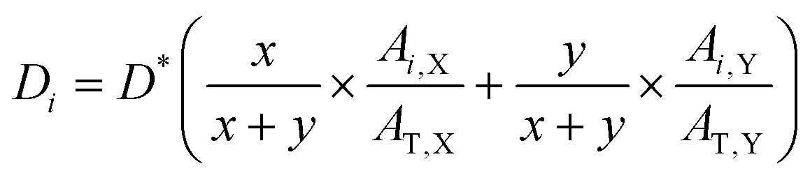 | (2) |
:Y equals to x:y. Ai,X and Ai,Y are the absorbance of X and Y in i sublayer, which can be calculated from the FDD-IR spectroscopy. AT,X and AT,Y, obtained from the infrared spectrum before etching, are the total absorbance of X and Y in the whole blend films, respectively. For the accuracy of the experiment results, the peak area was utilized as the absorbance.
Characterization
All infrared spectroscopy measurements were conducted via Thermo Scientific Nicolet 6700 in ambient. CaF2 substrate were used for all of the test films.The surface-selective-etching process were all conducted by a Femto plasma cleaner (Diener Electronic GmbH & Co.KG) under the condition of argon plasma pressure below 30 Pa and glow discharge frequency 13.56 MHz.
The current density–voltage (J–V) characteristics of the photovoltaic devices were measured in the glove box by a Keithley 2400 Source-Measure unit. A Newport solar simulator was utilized to measure the performance of devices under AM1.5G (100 mW cm−2), which was calibrated using a standard Si photodiode detector for light intensity.
The transistors were measured with an Agilent Keysight B2900A Quick IV system in ambient. Drain–source voltage (VD) was fixed at −60 V for all transfer characteristics measurements.
Conflicts of interest
There are no conflicts to declare.Acknowledgements
This work was financially supported by the National Natural Science Foundation of China (51873172, 51907148), the China Postdoctoral Science Foundation (2018M643648), and the Fundamental Research Funds for the Central Universities (xjh012019023, xyz022019017). In particular, J. Yu is very grateful to Xianglong Li's assistance in OFETs, Yunzhao Li and Shuheng Zhao's infrared measurement in doped OSCs, Xiang Fen, Tong Xiao and Yupeng Hu's smart data handling, and Wanlong Lu's film fabrication in doped OSCs.References
- O. Ostroverkhova, Chem. Rev., 2016, 116, 13279 CrossRef CAS PubMed.
- J. Ahmad, K. Bazaka, L. J. Anderson, R. D. White and M. V. Jacob, Renewable Sustainable Energy Rev., 2013, 27, 104 CrossRef CAS.
- Y. Gu, C. Wang and T. P. Russell, Adv. Energy Mater., 2012, 2, 683 CrossRef CAS.
- E. F. Manley, J. Strzalka, T. J. Fauvell, T. J. Marks and L. X. Chen, Adv. Energy Mater., 2018, 8, 1800611 CrossRef.
- T. Xiao, J. Wang, S. Yang, Y. Zhu, D. Li, Z. Wang, S. Feng, L. Bu, X. Zhan and G. Lu, J. Mater. Chem. A, 2020, 8, 401 RSC.
- R. Steyrleuthner, R. Di Pietro, B. A. Collins, F. Polzer, S. Himmelberger, M. Schubert, Z. Chen, S. Zhang, A. Salleo, H. Ade, A. Facchetti and D. Neher, J. Am. Chem. Soc., 2014, 136, 4245 CrossRef CAS PubMed.
- I. E. Jacobs, C. Cendra, T. F. Harrelson, Z. I. B. Valdez, R. Faller, A. Salleo and A. J. Moule, Mater. Horiz., 2018, 5, 655 RSC.
- Z. Wang, Y. Hu, T. Xiao, Y. Zhu, X. Chen, L. Bu, Y. Zhang, Z. Wei, B. B. Xu and G. Lu, Adv. Opt. Mater., 2019, 7, 1900152 CrossRef.
- I. Lange, J. C. Blakesley, J. Frisch, A. Vollmer, N. Koch and D. Neher, Phys. Rev. Lett., 2011, 106, 216402 CrossRef PubMed.
- L. Bu, S. Gao, W. Wang, L. Zhou, S. Feng, X. Chen, D. Yu, S. Li and G. Lu, Adv. Electron. Mater., 2016, 2, 1600359 CrossRef.
- L. Zhou, L. Bu, D. Li and G. Lu, Appl. Phys. Lett., 2017, 110, 093301 CrossRef.
- M. Schubert, D. Dolfen, J. Frisch, S. Roland, R. Steyrleuthner, B. Stiller, Z. Chen, U. Scherf, N. Koch, A. Facchetti and D. Neher, Adv. Energy Mater., 2012, 2, 369 CrossRef CAS.
- Y. Lin, J. Wang, Z. G. Zhang, H. Bai, Y. Li, D. Zhu and X. Zhan, Adv. Mater., 2015, 27, 1170 CrossRef CAS PubMed.
- X. Xu, K. Feng, Z. Bi, W. Ma, G. Zhang and Q. Peng, Adv. Mater., 2019, 31, 1901872 CrossRef PubMed.
- Y. Cui, H. Yao, J. Zhang, K. Xian, T. Zhang, L. Hong, Y. Wang, Y. Xu, K. Ma, C. An, C. He, Z. Wei, F. Gao and J. Hou, Adv. Mater., 2020, 32, 1908205 CrossRef CAS PubMed.
- H. Hase, K. O’Neill, J. Frisch, A. Opitz, N. Koch and I. Salzmann, J. Phys. Chem. C, 2018, 122, 25893 CrossRef CAS.
- K. F. Seidel, D. Lungwitz, A. Opitz, T. Kruger, J. Behrends, S. R. Marder and N. Koch, ACS Appl. Mater. Interfaces, 2020, 12, 28801 CrossRef CAS PubMed.
- S. Ninomiya, K. Ichiki, H. Yamada, Y. Nakata, T. Seki, T. Aoki and J. Matsuo, Rapid Commun. Mass Spectrom., 2009, 23, 1601 CrossRef CAS PubMed.
- P. Tyagi, M. K. Dalai, C. K. Suman, S. Tuli and R. Srivastava, RSC Adv., 2013, 3, 24553 RSC.
- Y. Yan, X. Liu and T. Wang, Adv. Mater., 2017, 29, 1601674 CrossRef PubMed.
- W. H. Lee, J. A. Lim, D. Kwak, J. H. Cho, H. S. Lee, H. H. Choi and K. Cho, Adv. Mater., 2009, 21, 4243 CrossRef CAS.
- K. Kang, S. Watanabe, K. Broch, A. Sepe, A. Brown, I. Nasrallah, M. Nikolka, Z. Fei, M. Heeney, D. Matsumoto, K. Marumoto, H. Tanaka, S. Kuroda and H. Sirringhaus, Nat. Mater., 2016, 15, 896 CrossRef CAS PubMed.
- V. Lami, A. Weu, J. Zhang, Y. Chen, Z. Fei, M. Heeney, R. H. Friend and Y. Vaynzof, Joule, 2019, 3, 2513 CrossRef CAS.
- G. Lu, J. Blakesley, S. Himmelberger, P. Pingel, J. Frisch, I. Lieberwirth, I. Salzmann, M. Oehzelt, R. Di Pietro, A. Salleo, N. Koch and D. Neher, Nat. Commun., 2013, 4, 1588 CrossRef PubMed.
- J. Wang, J. Zhang, Y. Xiao, T. Xiao, R. Zhu, C. Yan, Y. Fu, G. Lu, X. Lu, S. R. Marder and X. Zhan, J. Am. Chem. Soc., 2018, 140, 9140 CrossRef CAS PubMed.
- Y. Huo, X.-T. Gong, T.-K. Lau, T. Xiao, C. Yan, X. Lu, G. Lu, X. Zhan and H.-L. Zhang, Chem. Mater., 2018, 30, 8661 CrossRef CAS.
- Q. Liang, X. Jiao, Y. Yan, Z. Xie, G. Lu, J. Liu and Y. Han, Adv. Funct. Mater., 2019, 29, 1807591 CrossRef CAS.
- K. Weng, L. Ye, L. Zhu, J. Xu, J. Zhou, X. Feng, G. Lu, S. Tan, F. Liu and Y. Sun, Nat. Commun., 2020, 11, 2855 CrossRef CAS PubMed.
- B. B. Lahiri, S. Bagavathiappan, T. Jayakumar and J. Philip, Infrared Phys. Technol., 2012, 55, 221 CrossRef CAS PubMed.
- J. F. Lovell, C. S. Jin, E. Huynh, H. Jin, C. Kim, J. L. Rubinstein, W. C. Chan, W. Cao, L. V. Wang and G. Zheng, Nat. Mater., 2011, 10, 324 CrossRef CAS PubMed.
- L. Clarisse, C. Clerbaux, F. Dentener, D. Hurtmans and P.-F. Coheur, Nat. Geosci., 2009, 2, 479 CrossRef CAS.
- K. L. Gu, Y. Zhou, W. A. Morrison, K. Park, S. Park and Z. Bao, ACS Nano, 2018, 12, 1473 CrossRef CAS PubMed.
- N. E. Persson, P. H. Chu, M. McBride, M. Grover and E. Reichmanis, Acc. Chem. Res., 2017, 50, 932 CrossRef CAS PubMed.
- A. Marrocchi, D. Lanari, A. Facchetti and L. Vaccaro, Energy Environ. Sci., 2012, 5, 8457 RSC.
- R. Ben Gadri, J. R. Roth, T. C. Montie, K. Kelly-Wintenberg, P. P. Y. Tsai, D. J. Helfritch, P. Feldman, D. M. Sherman, F. Karakaya, Z. Y. Chen and U. T. K. P. S. Team, Surf. Coat. Technol., 2000, 131, 528 CrossRef CAS.
- H. Yoshiki, Jpn. J. Appl. Phys., 2010, 49, 08JJ02 CrossRef.
- N. Kireche, S. Rondot, F. Bitam-Megherbi, O. Jbara, M. Gilliot and J.-M. Patat, Eur. Phys. J.: Appl. Phys., 2018, 82, 31301 CrossRef CAS.
- S. K. Nemani, R. K. Annavarapu, B. Mohammadian, A. Raiyan, J. Heil, M. A. Haque, A. Abdelaal and H. Sojoudi, Adv. Mater. Interfaces, 2018, 5, 1801247 CrossRef.
- J. Li, Y. Zhao, H. S. Tan, Y. Guo, C. A. Di, G. Yu, Y. Liu, M. Lin, S. H. Lim, Y. Zhou, H. Su and B. S. Ong, Sci. Rep., 2012, 2, 754 CrossRef PubMed.
- J. Yuan, Y. Zhang, L. Zhou, G. Zhang, H.-L. Yip, T.-K. Lau, X. Lu, C. Zhu, H. Peng, P. A. Johnson, M. Leclerc, Y. Cao, J. Ulanski, Y. Li and Y. Zou, Joule, 2019, 3, 1140 CrossRef CAS.
- Y. Chang, T.-K. Lau, M.-A. Pan, X. Lu, H. Yan and C. Zhan, Mater. Horiz., 2019, 6, 2094 RSC.
- Y. Ma, X. Zhou, D. Cai, Q. Tu, W. Ma and Q. Zheng, Mater. Horiz., 2020, 7, 117 RSC.
- C. B. Nielsen, M. Turbiez and I. McCulloch, Adv. Mater., 2013, 25, 1859 CrossRef CAS PubMed.
- H. Yao, L. Ye, H. Zhang, S. Li, S. Zhang and J. Hou, Chem. Rev., 2016, 116, 7397 CrossRef CAS PubMed.
- J. Hou, O. Inganas, R. H. Friend and F. Gao, Nat. Mater., 2018, 17, 119 CrossRef CAS PubMed.
- Y. Yuan, G. Giri, A. L. Ayzner, A. P. Zoombelt, S. C. Mannsfeld, J. Chen, D. Nordlund, M. F. Toney, J. Huang and Z. Bao, Nat. Commun., 2014, 5, 3005 CrossRef PubMed.
- C. Teixeira da Rocha, K. Haase, Y. Zheng, M. Löffler, M. Hambsch and S. C. B. Mannsfeld, Adv. Electron. Mater., 2018, 4, 1800141 CrossRef.
- S. Han, X. Yu, W. Shi, X. Zhuang and J. Yu, Org. Electron., 2015, 27, 160 CrossRef CAS.
- L. Yang, S. Zhang, C. He, J. Zhang, H. Yao, Y. Yang, Y. Zhang, W. Zhao and J. Hou, J. Am. Chem. Soc., 2017, 139, 1958 CrossRef CAS PubMed.
- G. Lu, R. D. Pietro, L. S. Kölln, I. Nasrallah, L. Zhou, S. Mollinger, S. Himmelberger, N. Koch, A. Salleo and D. Neher, Adv. Electron. Mater., 2016, 2, 1600267 CrossRef.
- E. F. Aziz, A. Vollmer, S. Eisebitt, W. Eberhardt, P. Pingel, D. Neher and N. Koch, Adv. Mater., 2007, 19, 3257 CrossRef CAS.
- K. E. Watts, B. Neelamraju, E. L. Ratcliff and J. E. Pemberton, Chem. Mater., 2019, 31, 6986 CrossRef CAS.
Footnote |
| † Electronic supplementary information (ESI) available. See DOI: 10.1039/d0mh02047h |
| This journal is © The Royal Society of Chemistry 2021 |