
 Open Access Article
 This Open Access Article is licensed under a
 Creative Commons Attribution 3.0 Unported Licence
Dislocation-toughened ceramics†
Lukas
Porz
 *a,
Arne J.
Klomp
a,
Xufei
Fang
a,
Ning
Li
b,
Can
Yildirim
c,
Carsten
Detlefs
c,
Enrico
Bruder
a,
Marion
Höfling
a,
Wolfgang
Rheinheimer
ad,
Eric A.
Patterson
ae,
Peng
Gao
b,
Karsten
Durst
a,
Atsutomo
Nakamura
fg,
Karsten
Albe
a,
Hugh
Simons
h and
Jürgen
Rödel
*a
*a,
Arne J.
Klomp
a,
Xufei
Fang
a,
Ning
Li
b,
Can
Yildirim
c,
Carsten
Detlefs
c,
Enrico
Bruder
a,
Marion
Höfling
a,
Wolfgang
Rheinheimer
ad,
Eric A.
Patterson
ae,
Peng
Gao
b,
Karsten
Durst
a,
Atsutomo
Nakamura
fg,
Karsten
Albe
a,
Hugh
Simons
h and
Jürgen
Rödel
*a
aTechnical University of Darmstadt, Department of Materials and Earth Science, Darmstadt, Germany. E-mail: porz@ceramics.tu-darmstadt.de; roedel@ceramics.tu-darmstadt.de
bPeking University, Beijing, China
cEuropean Synchrotron Radiation Facility, Grenoble, France
dForschungszentrum Jülich GmbH, Jülich, Germany
eU.S. Naval Research Laboratory, Materials Science and Technology Division, Washington DC, USA
fDepartment of Materials Physics, Nagoya University, Nagoya, Japan
gPRESTO, Japan Science and Technology Agency, Tokyo, Japan
hDepartment of Physics, Technical University of Denmark, Kongens Lyngby, Denmark
First published on 16th March 2021
Abstract
Functional and structural ceramics have become irreplaceable in countless high-tech applications. However, their inherent brittleness tremendously limits the application range and, despite extensive research efforts, particularly short cracks are hard to combat. While local plasticity carried by mobile dislocations allows desirable toughness in metals, high bond strength is widely believed to hinder dislocation-based toughening of ceramics. Here, we demonstrate the possibility to induce and engineer a dislocation microstructure in ceramics that improves the crack tip toughness even though such toughening does not occur naturally after conventional processing. With modern microscopy and simulation techniques, we reveal key ingredients for successful engineering of dislocation-based toughness at ambient temperature. For many ceramics a dislocation-based plastic zone is not impossible due to some intrinsic property (e.g. bond strength) but limited by an engineerable quantity, i.e. the dislocation density. The impact of dislocation density is demonstrated in a surface near region and suggested to be transferrable to bulk ceramics. Unexpected potential in improving mechanical performance of ceramics could be realized with novel synthesis strategies.
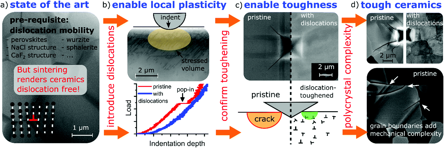
New conceptsThe brittle nature of ceramics limits their application range decisively despite their importance for key technologies. For decades, materials scientists appreciated the high bond strength of ceramics and accepted the absence of a toughness-enhancing plastic zone. Hence, the possibility of toughening ceramics by engineering mobile dislocations to form a plastic zone around crack tips, as it occurs naturally in metals, was hardly considered. This is surprising as dislocations are mobile at room temperature in a whole range of ceramic materials. However, the mere mobility of dislocations does not directly lead to a plastic zone at crack tips which enhances toughness. Here, we extensively investigate the dislocation behavior with a range of methods from dark-field X-ray microscopy and ultra-high voltage electron microscopy to indentation and molecular dynamics culminating in a simple conclusion: plastic zones in ceramics at crack tips are available to toughen ceramics after all; only – a large number of dislocations is required. After introducing a suitable dislocation density, we demonstrate that local plasticity is successfully enabled and provide evidence for toughening ceramics by dislocations. This seemingly simple realization opens up a range of new opportunities far beyond our current imagination. Conventional sintering, the standard densification method for ceramics, actually yields ceramics virtually free of dislocations and dislocation sources. In other words, the brittleness of ceramics appears as merely a consequence of the established conventional production method. |
Introduction
Ceramics are considered as inherently brittle. Widely accepted understanding states that a toughness-enhancing plastic zone in ceramics based on dislocations “would require changing the bond strength” which is “not a feasible undertaking”.1 In metals, in contrast, the availability of mobile dislocations results in high plastic deformability and fracture toughness. Although a large number of single crystalline ceramics can be deformed by dislocation movement at room temperature, dislocations have only rarely been connected to fracture toughness in ceramics.2,3 Instead, tremendous effort was focused on alternative mechanisms to toughen ceramics primarily in the 1980s.1,4 These efforts centered on shielding the crack tip from the applied load leading to R-curve behavior where toughness is gained only after an advancement of the crack.1,4 This entails the dilemma that only long cracks create tough ceramics and, hence, only limited load-bearing capacity and low crack tolerance can be obtained.In fact, it is strikingly easy to move dislocations in many ceramics even at cryogenic temperatures5–7 with evidence from indentation8–10 and single crystal compression (e.g. for LiF,5 MgO,6 SrTiO311). Even though dislocations can move and ceramic single crystals are ductile, they, nevertheless, feature a low fracture toughness. Why?
Once dislocations are mobile, the ability of a material to nucleate dislocations at a crack tip is considered to be a further pre-requisite for a toughness enhancement by dislocations.12 While a nucleation of dislocations at crack tips13 readily occurs in metals and assures the supply of dislocations where needed, it occurs only to a very limited degree in ceramics13,14 (e.g. absent in SrTiO3, see supplementary 1, ESI†). This results in the general belief that dislocations cannot toughen ceramics due to high bond strength and the inability to nucleate dislocations at crack tips at low temperatures.
Indications to the opposite are available but rare: MgO features dislocation activity at the crack tip at low crack velocity15 and a very high crack-tip toughness of KI0 = 9.8 MPa  14,16 under plane stress conditions in thin TEM samples. This value lies between typical toughness values for ceramics (e.g., Al2O3: KIc = 3 MPa
  )17 and FCC metals (e.g., Aluminum: KIc = 30 MPa
  ).18
).18
But can a dislocation-based toughness-enhancing plastic zone be engineered into ceramics even though dislocations do not naturally nucleate at the crack tip? If so, this would allow new avenues for toughening ceramics and vastly expand applications. In particular it would empower us to combat short cracks and crack formation.
In the following, we demonstrate that the absence of local plasticity in ceramics does not hinge on bond strength but is intimately related to the availability of pre-existing dislocations in the volume around the crack tip (and grain boundary). Separation of motion and multiplication from nucleation allows us to predict that a high pre-existing dislocation density yields dislocation toughening. Subsequently we insert a high dislocation density of 5 × 10¹⁴ m−2 into the model material SrTiO3 and demonstrate its impact both on local plasticity and toughness.
Dislocation-toughening
First, we quantify the influence of pre-existing dislocations on the stress intensity factor and relate to typical dislocation densities. In principle, the individual contributions of i (edge) dislocations on the stress intensity at a crack tip can be summed up by factoring in the distance xi from the crack tip12 as
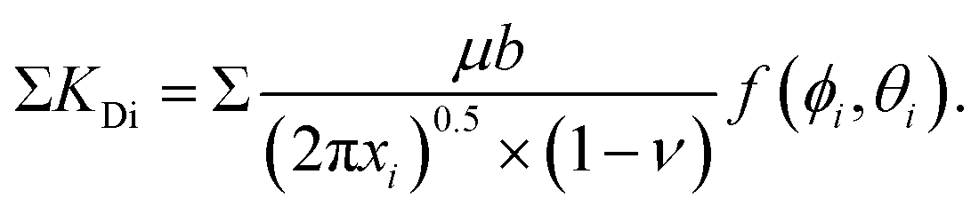 | (1) |
![[1 with combining macron]](https://www.rsc.org/images/entities/char_0031_0304.gif) 0} slip system and 0.237,20 respectively, for SrTiO3). f(ϕi,θi) is a function of the angle between crack plane and slip plane (ϕi) and the line joining the crack tip to the dislocation (θi). The radius x of the plastic zone is rendered using the yield stress for SrTiO3, σys = 120 MPa and its pristine crack tip toughness, KI0 = 0.75 MPa
0} slip system and 0.237,20 respectively, for SrTiO3). f(ϕi,θi) is a function of the angle between crack plane and slip plane (ϕi) and the line joining the crack tip to the dislocation (θi). The radius x of the plastic zone is rendered using the yield stress for SrTiO3, σys = 120 MPa and its pristine crack tip toughness, KI0 = 0.75 MPa  (as measured below) as
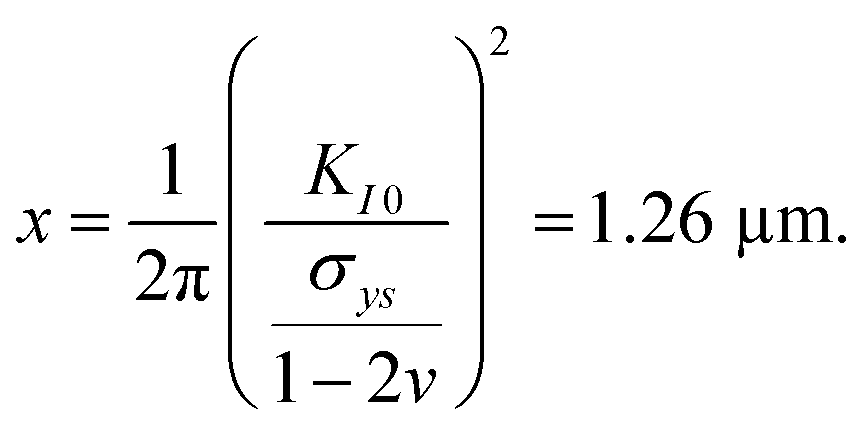 | (2) |
Note that a typical dislocation density of 1010 m−2 (see supplementary 2, ESI†) cannot provide toughening as statistically only 0.05 dislocations can be found in the area πx2 at the crack tip explaining why natural toughening (i.e. by the pre-existing dislocations) is not typically observed. In contrast, if for example 500 dislocations were ideally oriented (f(ϕi,θi) = 1) at a distance of xi = 1.26 μm, the sum of the toughening contribution would amount to 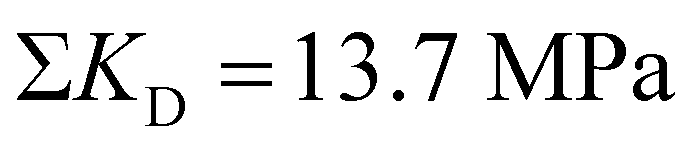
 (an 18-fold increase over
  ). This would require a mobile dislocation density of 1014 m−2. A more precise description, adding substantial complexity, would need to take into account the exact arrangement of dislocations which are rearranged by the stress field of the crack tip. This simple realization already reveals that, for most ceramics, a dislocation-based plastic zone is not hindered by an insurmountable intrinsic property (bond strength) but by an engineerable quantity, which is the dislocation density.
Dislocation structure
Being aware of the necessity of high dislocation densities, we investigate the dislocation structure at a microscopic level with the ultimate goal of finding guidelines for engineering dislocation microstructure. We will elaborate how dislocations in ceramics propagate, multiply and nucleate (demonstrated using SrTiO3 as model material).Select ceramic single crystals, with the room temperature 〈110〉{110} slip system of SrTiO3 as well studied example,11 can be extensively deformed by uniaxial compression7,21 which enhances dislocation density.19 Dislocations arrange in slip bands with a density of 2 × 10¹³ m−2 (see Fig. 1a) on parallel slip planes. This behavior is well investigated also for LiF as well as other ceramic single crystals.5
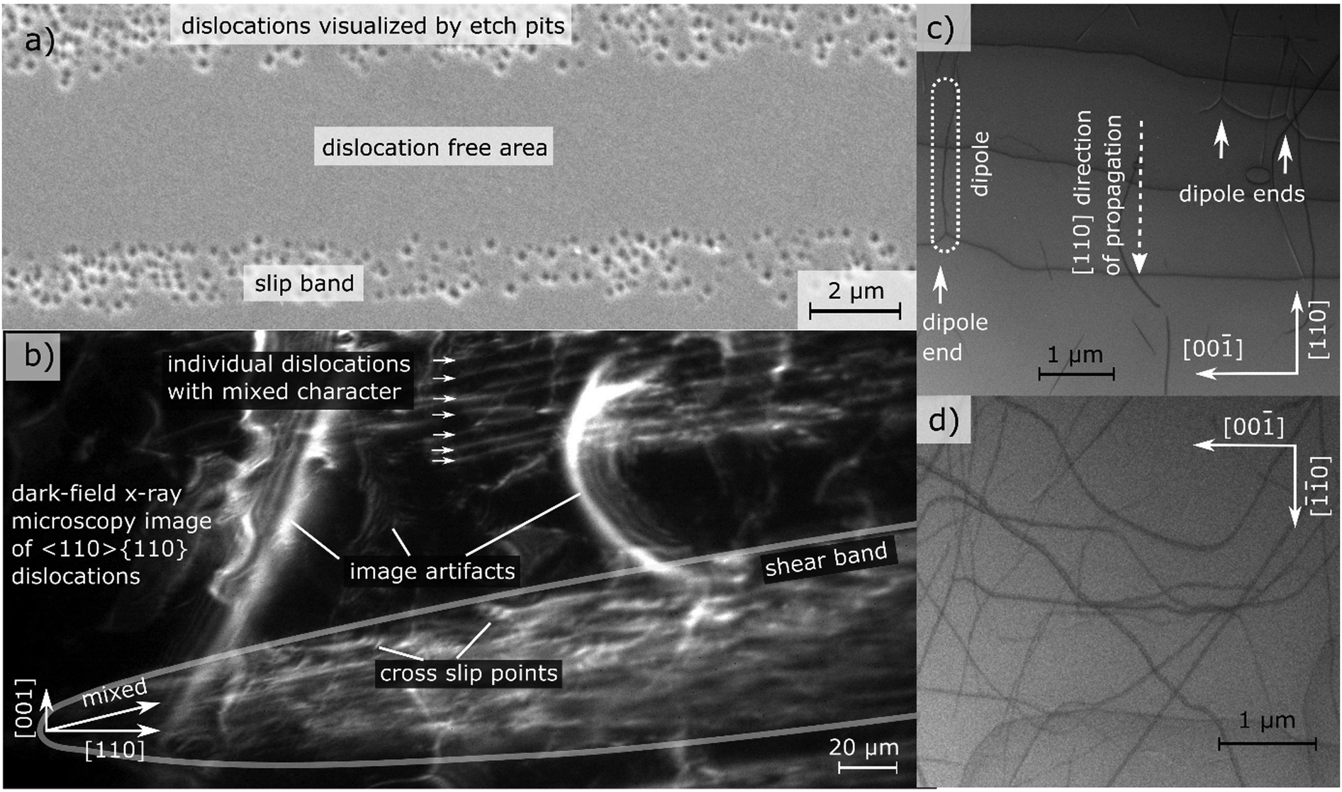 | ||
| Fig. 1 Analysis of dislocation structure of slip bands in uniaxially compressed SrTiO3 single crystals. (a) SEM image of slip bands and individual dislocations visualized by etching. (b) Excerpts from supplementary 3 (video) (ESI†): Individual dislocations inside a slip band observed with dark-field X-ray microscopy. Individual dislocations at the tip of a slip band are visible over more than 100 μm. The dislocation sub-structure of an entire slip band is highlighted and cross-slip points can be identified from tilted perspective in the supplementary video (ESI†). (c) and (d) Ultra-high voltage electron microscopy images (BF-STEM) of two different regions of a slip band where (c) is imaged close to the tip of the slip band while (d) is viewed approximately 20 μm behind the tip. Multiple dislocation dipoles originating from jog dragging25,26 can be identified. The analysis of the Burgers vector, is depicted in supplementary 8 (ESI†). Adapted with permission from Porz et al., ACS Nano, DOI: 10.1021/acsnano.0c04491. Copyright (2020) American Chemical Society. | ||
Dark-field X-ray microscopy (DFXM)22,23 allows monitoring dislocations inside of slip bands formed by deformation within a 200 μm thick bulk sample providing insight in the mechanisms of deformation. In order to not obscure DFXM images with natural dislocations (and exclude their effect), SrTiO3 single crystals grown by top seeded solution growth with particularly low natural dislocation density were used for DFXM.24 In supplementary 3 (video) (ESI†) the sample is tilted in various angles using topo-tomography.22,23 At the tip of a band, where the spacing is large, individual dislocations can be discerned clearly (Fig. 1b).
A large number of dislocation lines can be observed to link up between several lattice planes, best visible in 3D at slight tilt (see Fig. 1b and supplementary 3 (video), ESI†). The slip band can be identified as a complex structure that extends almost equally in two dimensions and has a certain width in the third dimension. Here, several sites of multiple cross slip (each larger than 20 μm) can be observed due to the large field of view, see Fig. 1b. The cross slip enables Koehler sources, a multiplication mechanism creating new dislocations of same and opposite line vector on adjacent lattice planes.27,28 From three-dimensional data on strain and mosaicity (lattice tilt, see supplementary 4–7, ESI†) acquired by layered imaging, we conclude that the strain fields overlap locally with no long-range strain fields around the bands. Additionally, we note the abundance of dislocation multiplication while we find no evidence for dislocation nucleation.
A contrast of DFXM images with TEM images allows verifying the mesoscopic dislocation structure observed inside of a band over a scale of hundreds of μm. This comparison confirms that the volume was, in fact, previously free of dislocations. Ultra-high voltage electron microscopy (UHVEM) is used to identify the dislocation orientation. In regions close to the slip band front with low dislocation density, edge-type dislocations on {10} planes with b = [110] Burgers vector are predominantly found. Furthermore, the dislocation propagation direction, 〈110〉, can be inferred from the orientation of the dipoles dragged behind jogs in Fig. 1c.25,26 Further behind the tip, the dislocation structure becomes much more complex and reveals more screw and mixed components (Fig. 1d).
A more detailed investigation by HAADF-STEM focused on a FIB-lamella from a slip band reveals dissociation of dislocations into two partials11,21 (see supplementary 9, ESI†). The configuration is climb-dissociated (see supplementary 10 (ESI†) and Fig. 2a and b) with a climb distance of three unit cells, which is most likely induced by the electron beam activation. Approximately half of the 13 dislocations investigated at atomic resolution were found in a dipole configuration consisting of two dislocations dissociated into two partials each (see Fig. 2c and d). The distance between the dipoles, is less than 15 unit cells (Fig. 2d). When the temperature is sufficient for climb dissociation, recombination of the dipoles should be possible with similar thermal activation. Since dislocation dipoles are also known as origin of dislocation multiplication,25,29 a recombination is expected to hinder dislocation multiplication. The temperature range for recombination is found to coincide with the ductile to brittle transition in SrTiO311,30 as the amount of dislocations in a deformed crystal is significantly reduced when annealing at 900 °C (see supplementary 11, ESI†).
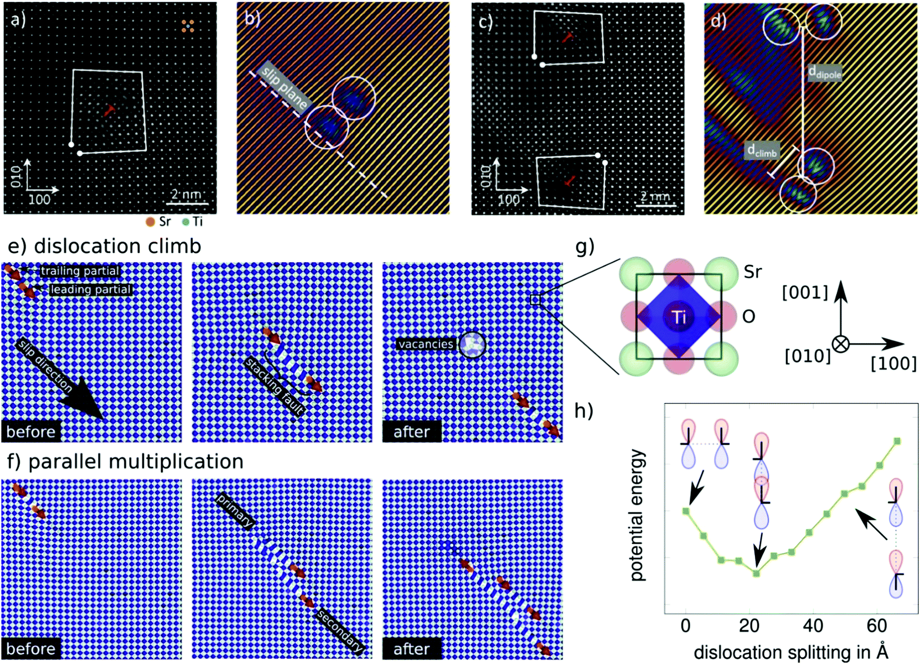 | ||
| Fig. 2 Dislocation structure at atomic resolution. (a) HAADF image of the dislocation core of a 〈110〉{110} type dislocation with Burgers circuit. (b) Atom planes corresponding to (a), illustrating that the partial dislocations have climb-dissociated (see supplementary 10, ESI†), likely due to the electron beam. (c) Dislocations in close vicinity with less than 15 unit cells distance revealing opposite line vectors. (d) Atom planes corresponding to (c). (e) Molecular dynamics simulations highlight spontaneous climb of a dislocation and creation of a defective region with vacancies. Dislocation lines are indicated in orange and the direction of the Burgers vector as red arrow. (f) One of two dislocation partials climbs to a parallel (secondary) glide plane while the other stays on its original (primary) plane. New partials spawn to complete the singular partials. On the lower plane an extended stacking fault is created between the partials which is relieved by creating further partial dislocations effectively multiplying the dislocation. (g) Representation of a SrTiO3 unit cell. The blue shapes represent polyhedra of oxygen around titanium and are well suited to identify defects such as stacking faults. For clarity the oxygen atoms are not shown in (e) and (f). (h) Dependence of the energy of two partial dislocations on their separation distance in climb dissociation. Partial dislocations of the shown type have a tendency to climb, see (a–d) as well as (e) and (f), which is energetically favored over dissociation in slip direction. For full details see Supplementary 12 (ESI†). (a-d) reprinted with permission from Porz, et al., ACS Nano, DOI: 10.1021/acsnano.0c04491. Copyright (2020) American Chemical Society. | ||
In the following, we use molecular dynamics simulations to extend the picture of dissociated 〈110〉{110}-type dislocations from a static observation after deformation to a mechanistic insight into dislocation structure evolution (for details see supplementary 12 (ESI†)31,32). A model experiment33 provides a local stress concentration under compressive loading and yields well defined mobile dislocations in pure SrTiO3. As expected, we observe edge dislocation partials nucleating at surface defects. These dislocations propagate easily through the material under applied compressive stress. However, dislocations rarely traverse the crystal in a completely straight line, see supplementary video 13 (ESI†). In fact, the modeled dislocation segments climb spontaneously changing their glide plane by one atomic layer. In turn, the partial dislocations climb which gives rise to a new field of creating local defects (e.g. vacancies) and dislocation multiplication mechanisms. Examples for spontaneous climb and a dislocation multiplication during dislocation motion are given in Fig. 2e and f, respectively. A closer inspection of the dissociated dislocation reveals that climb dissociation is energetically favored over glide dissociation (Fig. 2h).30,34
Quantification of toughening
A proof-of-concept for dislocation toughening of ceramics requires a suitably high dislocation density. To engineer dislocation densities beyond 1014 m−2, we apply a simple polishing procedure (Jin et al.35), which, however, impacts only a surface layer of about 5 μm. The statistic nature of point contacts of polishing particles with the surface abundantly nucleates dislocations and activates all available 〈110〉{110} type slip systems.10 Toughening in this thin layer is assessed in the following.Deforming a volume with engineered high dislocation density only requires dislocation mobility but not dislocation nucleation. The locally increased plasticity can easily be verified using nano-indentation.9,10 For a dislocation-free volume, elastic behavior up to the theoretical shear stress is observed before a transition to elasto-plastic behavior. As this ‘pop-in’ occurs at ∼17 GPa in Fig. 3a, dislocations are nucleated homogeneously for sharp indenters36 (see Fig. 3a and b). Appropriate choice of tip radius defines the probed volume with radius equal to x of the plastic zone calculated in eqn (2).9,10 If a sufficient density of dislocations can be provided (see Fig. 3c and d), plastic flow sets in far below the theoretical shear stress.9,10 Accordingly, immediate plastic deformation without pop-in ensues (Fig. 3c). Fig. 3e provides a distribution of pop-in stresses for pristine surfaces and dislocation-engineered surfaces (ρ = 5 × 10¹⁴ m−2 distributed over all mobile slip systems,35 see supplementary 14, ESI†). In contrast, an indentation into a slip band reduces the pop-in stress only marginally as the local dislocation density is only 2 × 10¹³ m−2. This complete transition from nucleation to mobility controlled behavior arises from the vastly different densities of dislocations and calls for a quantification of fracture toughness in the volume of high dislocation density.
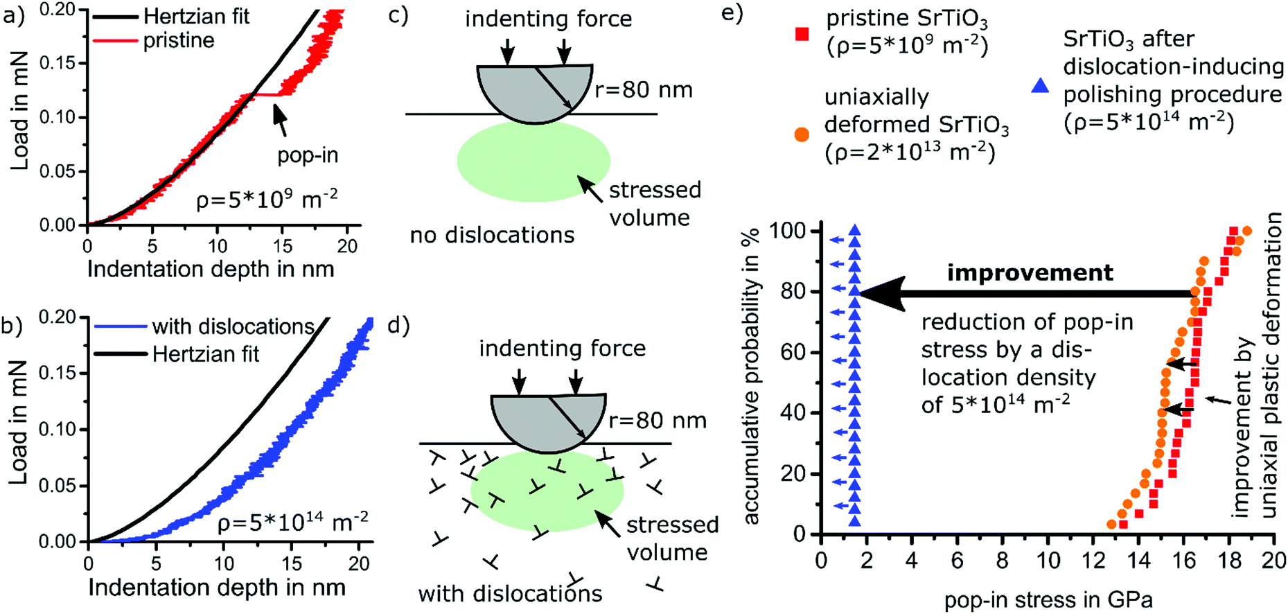 | ||
| Fig. 3 Enhancement of local plasticity probed with nanoindentation on {100} surfaces of SrTiO3 single crystals. (a) Representative load–displacement curves into a pristine surface with pop-in and (b) a surface with dislocation density of 5 × 10¹⁴ m−2 without pop-in (see supplementary 14 and 15, ESI†). The latter features ideal plastic behavior down to low loads. (c) and (d) Schematic drawings of the indentation site corresponding to the load–displacement curves of (a) and (b), respectively. (e) Statistical evaluation of the pop-in stress for different dislocation densities underpinning the large enhancement of local plasticity by a pre-existing high dislocation density. Blue triangles with arrow on the left indicate the absence of a pop-in. (The lower detection limit of 1.5 GPa is related to the accuracy limit of the machine employed). | ||
As the induced high dislocation density is confined to a less than 5 μm thick surface layer,35 fracture toughness needs to be tested locally. Therefore, we resort to a direct evaluation of the crack tip opening displacement of a loaded crack in order to provide a quantification of crack-tip toughness, KI0.14,37,38 When indenting on a (100) surface with a Vickers indenter using 98.1 mN load, cracks were confined to the surface layer thickness with high dislocation density. A pristine SrTiO3 single crystal produces cracking as illustrated in Fig. 4a and c. In contrast, after introducing a dislocation density of 5 × 10¹⁴ m−2 at the surface, cracking is inhibited completely (Fig. 4b and d). As this surface appears to be too tough for quantification in the dislocation-rich surface regime, an orientation with less toughening was considered.
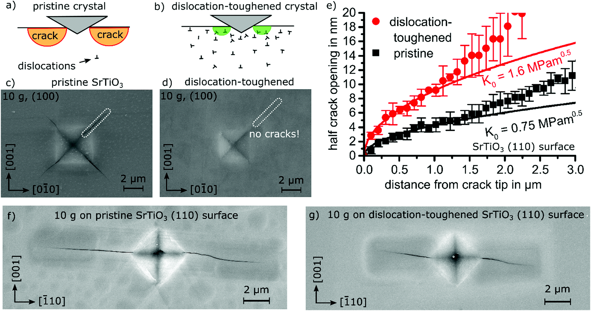 | ||
| Fig. 4 Effect of dislocations on fracture toughness in SrTiO3. (a) Sketch of Vickers indents inducing cracks at the surface in a pristine crystal and (b) in a region with high dislocation density where crack formation can either be completely suppressed or the crack length strongly reduced. (c) Vickers indent on a pristine SrTiO3 single crystal (100) surface revealing distinct crack formation. (d) Same indent on a dislocation-toughened SrTiO3 single crystal surface displaying no cracks. (e) Crack tip opening displacement on the dislocation-toughened (110) surface indicating a doubling in crack tip toughness (details in supplementary 16, ESI†). (f) Vickers indent on a pristine SrTiO3 (110) surface and (g) a (110) surface after dislocation-inducing polishing. | ||
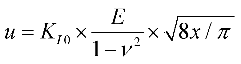
On the (110) surface of SrTiO3, cracks originate from only two corners of the indent which align with the {110} planes, see Fig. 4f (pristine surface) and 4g (toughened surface). The crack propagation direction is, thus, least favorably oriented towards the available slip planes and is deemed to provide the smallest toughening effect. In consequence, the crack tip opening displacement method37,38 can be applied for quantification, because the ratio of crack length to indent diagonal is larger than two (Fig. 4f and g).
The crack tip toughness KI014 is determined by fitting the initial square root-shaped crack opening displacement with the elastic displacement field for crack tips (see Experimental details). On the (110) surface, an increase of crack tip toughness beyond a factor of two from 0.75 MPa m1/2 to 1.6 MPa m1/2 is clearly related to the high dislocation density (see Fig. 4e). Our results demonstrate dislocation-induced toughening on two orientations of the model material SrTiO3 with an additional discussion on MgO in supplementary 17 (ESI†).
Discussion
While we observe an astonishing multitude of multiplication mechanisms at different length scales in addition to good dislocation mobility, we did not observe dislocation nucleation in the single crystals in uniaxial compression. Simultaneously we note that the dislocation density in both pristine single crystals and polycrystals (see supplementary 2, ESI†) is typically below 1010 m−2. This renders volumes with the size of 10 × 10 × 10 μm3 (e.g. entire grains) dislocation-free. When attempting to deform a dislocation-free volume, instead of the shear stress required to move a dislocation (such as 60 MPa for SrTiO37) the stress to (homogeneously) nucleate a dislocation (such as ∼17 GPa for SrTiO3, see Fig. 3) is required. Such nucleation step must be avoided.The volume in a uniaxially compressed single crystal is typically large enough to find at least one dislocation which can move and multiply and, hence, nucleation is not required. In polycrystals instead, grain boundaries impede the motion and each grain needs to be able to deform by itself, again requiring nucleation. The high nucleation stress10,39 then hinders a deformation of polycrystals. Accordingly the ductility observed in single crystalline ceramics is still often “surprising”7 or “unexpected”.40 However, as shown back in the 1960s, dislocation motion within some grains can lead to small but detectable macroscopic strains of polycrystalline ceramics,41 and even allows the formation of a plastic zone at crack tips (e.g. in MgO).42,43
The mechanical behavior of ceramics is then somewhat comparable to metals with extremely few dislocations.44 The formation of slip bands leads to nucleation of cracks at grain boundaries43 (also an origin of microcracking42) because slip transfer or alternatively nucleation on the other side of the grain boundary (secondary slip) requires high stresses.39 This can substantially limit an effective plastic zone as observed e.g. for MgO.42,43 Furthermore, we suggest that the presence of dislocations or nucleation39 at grain boundaries are both more pressing and more easily addressable concerns for small strains than the Taylor criterion.45 Taylor suggested that at least five geometrically independent slip systems are required to deform a polycrystal due to the mismatch of random crystallite orientations. In ceramics, typically less than five slip systems are mobile at room temperature limiting the deformation of polycrystals.46 However, this neither limits large local deformation nor small macroscopic deformation.
We conclude that a high density of appropriately oriented and mobile dislocations is not only required for enhancing crack tip toughness but also to allow secondary slip on the other side of a grain boundary in order to avoid (micro)crack initiation by pile-up of dislocations in slip bands. In supplementary 18 (ESI†), we demonstrate that slip band formation is suppressed by the dislocation structure. Furthermore, the provided dislocation structure substantially improves the cracking behavior of polycrystals (Fig. 5d and supplementary 19, ESI†).
 | ||
| Fig. 5 Essential steps for developing dislocation-toughened ceramics. (a) Sketch of a dislocation on atomic scale. Background: Bright-field scanning transmission electron microscope image demonstrating the absence of dislocations in as-sintered SrTiO3 samples. (b) Top: Ultra high voltage electron microscopy image (BF-STEM mode) of dislocations introduced by the dislocation-inducing polishing procedure overlaid with a sketch of an indenter. Bottom: Representative load–displacement curves from nano-indentation. (c) Top: SEM image confirming suppression of cracks by a dislocation density of 5 × 10¹⁴ m−2. Bottom: Corresponding schematic. (d) Top: SEM of Vickers indentation in polycrystalline SrTiO3 without (left) and with dislocations (right) confirming the toughening effect also for polycrystals. Bottom: Backscattered electron image of cracks close to a Vickers indent in pristine SrTiO3 revealing mechanical complexity in polycrystals. | ||
From the investigation above we learn that multiplication of dislocations alone does not lead to desired dislocation structures. As fracture will prevail if local dislocation nucleation is required, dislocation toughening in ceramics is within reach but demands high dislocation densities.
Steps for development
The concepts discussed above open new perspectives for tweaking the mechanical performance of ceramics by dislocation-toughening. The impact of dislocations (Fig. 5a) can be readily assessed using a quantification of indentation pop-in (Fig. 5b) and a visual inspection of the tendency for cracking around the elastic-plastic indentation zone (Fig. 5c). Preliminary experiments suggest that the toughening effect can be transferred to polycrystals (see Fig. 5d).For this new generation of dislocation-toughened ceramics, a high density of pre-existing dislocations (or suitable dislocation sources) is required, which calls for a rethinking of traditional processing strategies. While the effect in bulk polycrystals still awaits detailed investigations, the presented understanding will allow to make targeted efforts towards suitable processing strategies. Desirable dislocation structures could be achieved by plastic deformation after processing, e.g. by local,2 or high-pressure deformation.47 Fortunately, a suite of radically new densification techniques invented recently can result in a dislocation-rich microstructure. This could be the case, for example, for: (i) hydrothermal densification (cold sintering),48 (ii) the Aerosol Deposition Method (ADM)49 or (iii) ultrafast sintering based on rapid heating (e.g. flash sintering), resulting in ceramics with high dislocation density.50,51 With dislocation densities of >1014 m−2 revealed and already connected to improved mechanical behavior,51,52 there is considerable hope for applicability to bulk polycrystals.
Conclusions
We introduce the new concept of dislocation-toughening of ceramics by engineering a high dislocation density which enables formation of a crack tip plastic zone. High dislocation densities reduce the critical stress for plastic deformation by at least a factor of ten as assessed through a simple measurement of indentation pop-in. Concurrent enhancements of crack tip toughness by a factor of two have been obtained. The next step requires a synthesis method that efficiently introduces a sufficiently high dislocation density into the bulk ceramic. This has the potential to substantially toughen short cracks which may allow dramatically widening the application range of ceramics by increasing mechanical performance.Experimental
Crystal production and treatment
Two different SrTiO3 materials were used: For succinct mapping of the 3-dim. mesoscopic dislocation structure the highest quality SrTiO3 single crystal, devoid of any prior dislocations was needed.Towards this end, undoped top seeded solution grown single crystal SrTiO3 was produced at 1600 °C from TiO2 - rich solution by Daniel Rytz, FEE GmbH – A Division of EOT, Idar-Oberstein, Germany. The dimension was 1 × 1.2 × 2 mm3 into which a notch was introduced with a 170 μm diameter diamond wire saw into the long side. Deformation was done using a load frame (Z010, Zwick/Roell, Ulm, Germany) at room temperature in order to emanate slip bands from the notch but without the dislocations reaching the opposite free surface. Before deformation the surface was vibrationally polished. After deformation etching for 15–60 seconds in 15 ml 50% HNO3 with 16 drops of 48% HF was done. The thickness of the sample was reduced to 200 μm by grinding with SiC sand paper.
In parallel, Verneuil-grown SrTiO3 single crystals (Alineason GmbH, Frankfurt am Main, Germany) were cut to dimensions of 4 × 4 × 8 mm3 containing a natural dislocation density of 5 × 10⁹ m−2. These were then subjected to plastic deformation of 2% plastic strain. This material was used for TEM and indentation studies.
Pristine surfaces were prepared by careful polishing for 40 minutes with diamond particle size of 6 μm, 3 μm, 1 μm and then 1/4 μm and vibrational polishing for 15 hours with OP-S solution from Struers (Copenhagen, Denmark). This procedure removes all mechanically introduced dislocations and yields a pristine surface. A dedicated surface treatment referred to as “dislocation-inducing polishing procedure” in the text was developed to retain a high dislocation density at the surface but achieve the same pristine surface roughness. To this end, grinding with P2500 SiC sandpaper introduced a maximized density of dislocations at the surface and the subsequent polishing time for each diamond particle polishing step was reduced to 30 seconds and vibrational polishing limited to 40 minutes. This removes a much thinner layer from the surface but flattens it. Both (100) as well as (110) surfaces were investigated.
Mechanical testing at the surface
Nanoindentation tests were carried out to assess the critical shear stress to initiate dislocation plasticity by quantifying the pop-in load. To this end the continuous stiffness measurement (CSM) mode was utilized with a constant strain rate of 0.05 s−1 on the iNano system (Nanomechanics inc., USA) with a three-sided Berkovich diamond indenter (Synton MDP, Switzerland). A maximum load of 45 mN was set, and a harmonic displacement oscillation of 2 nm was applied with a frequency of 100 Hz. For each indentation condition at least 10 tests were performed and later averaged. The frame stiffness and tip area functions were calibrated on a fused silica reference according to the Oliver–Pharr method.53Macroscopic indentation to introduce cracks was performed separately using a Vickers tip and 98.1 mN load. The crack tip toughness of short radial indentation cracks was quantified by determining the crack opening displacement as function of distance to the crack tip in a scanning electron microscope at magnification of 100![[thin space (1/6-em)]](https://www.rsc.org/images/entities/char_2009.gif) 000 times. Vickers indentations of load 98.1 mN were placed into either pristine surfaces or surfaces with high dislocation density and then sputtered with carbon. About 24 hours after indentation the crack opening profile was recorded and the following equation used.
000 times. Vickers indentations of load 98.1 mN were placed into either pristine surfaces or surfaces with high dislocation density and then sputtered with carbon. About 24 hours after indentation the crack opening profile was recorded and the following equation used.
 | (3) |
It relates crack tip toughness KI0 to the half-opening u, distance to the crack tip, x, and elastic modulus, E as well as the Poisson's ratio ν.38,54 In detail, note that the crack is at equilibrium at the time of pop-in, but can be subject to subcritical crack growth in the 24 hours before quantification of the crack opening displacement. Strictly speaking, the crack tip stress intensity factor thus obtained provides a point on the velocity–stress intensity (v–K) curve, slightly below actual fracture toughness.55 However, the ratio of fracture toughness between pristine and dislocation-toughened sample is expected to not be affected.
Electron microscopy
Two samples with high dislocation density at the surface obtained by the dislocation-inducing polishing procedure were glued together to protect the surface layer. A slice was extracted perpendicular to this surface and thinned by conventional polishing and ion milling to afford observation of the gradient of dislocation density from the surface to the center of the sample. The acceleration voltage was set to 1 MeV in STEM mode using the JEOL JEM-1000k RS.Furthermore, a sample of 2% deformed SrTiO3 single crystal was cut in a 2° angle to the slip plane and thinned by conventional polishing and ion milling. The acceleration voltage was set to 1 MeV in BF-STEM mode using the JEOL JEM-1000k RS.
Electron channeling contrast imaging (ECCI) was utilized to quantify the density of surface dislocations in the scanning electron microscope (see also Fig. S15, ESI†). High resolution SEM images were acquired using the MIRA3-XMH SEM (TESCAN, Brno, Czech Republic) equipped with a 4-quadrant solid state BSE detector (DEBEN, Woolpit, UK).
From a 2% deformed SrTiO3 single crystal a slice was cut in a 2° angle to the slip plane so that a FIB-lamella could be prepared with the dislocation line along a [100] direction perpendicular to the lamella thickness. The FIB samples were prepared by FEI Strata DB 235. Using HAADF-STEM atomic resolution images were recorded at 300 kV using an aberration-corrected FEI Titan Cube Themis G2.
Dark-field X-ray microscopy
The experiments were carried out at beamline ID-06 of the European Synchrotron Radiation Facility. A (110) reflection (with the diffraction vector pointing 45° away from the notch and hence parallel to the Burgers vector) at 2θ = 16.86° using a beam with 15.5 keV was selected. The sample was tilted in 2θ to find optimum contrast and rotated around the diffraction vector to tilt the slip planes in the field of view.For the layer acquisition slices of approximately 400 nm thickness were chosen. A (110) reflection was selected as well, this time normal to the slip plane. The sample was tilted in steps of 0.005° from −0.05° to 0.05° off the diffraction maximum with rotation vectors being [100] and [110] vectors orthogonal to the (110) reflection. For each voxel the mosaicity (the angular position of the intensity maximum in two tilt directions) has been determined using Matlab on the Lichtenberg high performance computer at TU Darmstadt. With a separate scan, where the 2θ angle has been altered as well, the local lattice strain could be quantified in addition to the mosaicity.
Molecular dynamics
Classical molecular dynamics simulations were performed using the LAMMPS simulation software56 on the Lichtenberg high performance computer at TU Darmstadt. We created a slab-like SrTiO3 geometry to mimic the experiment on the notched single crystals using periodic boundary conditions along the direction of the notch and along the loading direction. After pre-straining and equilibration compressive stress was applied to the latter direction with a constant engineering strain rate of 1.42 × 10⁸ s−1. The analysis of defects was assisted by post-processing with the software OVITO making use of its dislocation extraction algorithm and atomic strain calculation.57,58 More details can be found in supplementary 11 (ESI†).Author contributions
The project was conceived and designed by L. P. and J. R. C. Y., C. D. and H. S. acquired the DFXM data. L. P. and H. S. evaluated the DFXM data. N. L. acquired the HAADF-STEM images under supervision of P. G. A. K. performed the molecular dynamics simulations under supervision of K. A. A. N. acquired the UHVEM images. W. R. provided polycrystalline samples. W. R. and M. H. helped maturing the theoretical and experimental steps. E. P. conducted preliminary experiments. E. B. acquired high-resolution SEM and ECCI images. X. F. and K. D. assisted with indentation data interpretation. All authors discussed the results and commented on the manuscript drafted by L. P.Conflicts of interest
A related patent has been filed by LP, AK, XF and JR under application number PCT/EP2021/052032.Acknowledgements
LP, MH and JR are greatly indebted to the Deutsche Forschungsgemeinschaft for funding under grant number 398795637 and 414179371. We are indebted to Daniel Rytz for discussions on dislocation contents in single crystal oxides. Furthermore, we acknowledge Xiaoxing Cheng, Henning Poulsen, Grethe Winter, Wolfgang Pantleon and Till Frömling for helpful discussions. NL and PG acknowledge the support from National Natural Science Foundation of China (51672007). We are grateful to the ESRF for providing beamtime at ID06. Calculations for this research were conducted on the Lichtenberg high performance computer of the TU Darmstadt. XF thanks the financial support from the Athene Young Investigator program at TU Darmstadt. WR acknowledges funding from the Deutsche Forschungsgemeinschaft under the Emmy-Noether-Program (RH 146/1). AN acknowledges the financial support of JST PRESTO Grant Number JPMJPR199A and JSPS KAKENHI Grant Numbers JP19H05786 and JP18H03840, Japan. Ultra-high voltage electron microscopy (UHVEM) observations in this work were conducted in Nagoya Univ., supported by Nanotechnology Platform Program of MEXT, Japan. We are grateful to Mr K. Higuchi for technical assistance with UHVEM experiments.Notes and references
- R. O. Ritchie, Nat. Mater., 2011, 10, 817–822 CrossRef CAS PubMed.
- W. J. Moon and H. Saka, Philos. Mag. Lett., 2000, 80, 461–466 CrossRef CAS.
- M. W. Chen, J. W. McCauley, D. P. Dandekar and N. K. Bourne, Nat. Mater., 2006, 5, 614–618 CrossRef CAS PubMed.
- A. G. Evans, J. Am. Ceram. Soc., 1990, 73, 187–206 CrossRef CAS.
- J. J. Gilman and W. G. Johnston, Solid State Phys., 1962, 13, 147–222 CAS.
- J. Amodeo, S. Merkel, C. Tromas, P. Carrez, S. Korte-Kerzel, P. Cordier and J. Chevalier, Crystals, 2018, 8, 240 CrossRef.
- D. Brunner, S. Taeri-Baghbadrani, W. Sigle and M. Rühle, J. Am. Ceram. Soc., 2001, 84, 1161–1163 CrossRef CAS.
- A. Montagne, V. Audurier and C. Tromas, Acta Mater., 2013, 61, 4778–4786 CrossRef CAS.
- Y. F. Gao and H. B. Bei, Prog. Mater. Sci., 2016, 82, 118–150 CrossRef CAS.
- X. Fang, L. Porz, K. Ding and A. Nakamura, Crystals, 2020, 10, 933 CrossRef CAS.
- S. Taeri, D. Brunner, W. Sigle and M. Rühle, Z. Metallkd., 2004, 95, 433–446 CrossRef CAS.
- P. B. Hirsch, in Plastic deformation of Ceramics, ed. R. C. Bardt, C. A. Brookes and J. L. Routbort, Springer Science + Business, New York, 1995 Search PubMed.
- J. R. Rice, J. Mech. Phys. Solids, 1992, 40, 239–271 CrossRef CAS.
- F. Appel, U. Messerschmidt and M. Kuna, Phys. Status Solidi A, 1979, 55, 529–536 CrossRef CAS.
- J. L. Robins, T. N. Rhodin and R. L. Gerlach, J. Appl. Phys., 1966, 37, 3893–3903 CrossRef CAS.
- U. Messerschmidt, Dislocation Dynamics during Plastic Deformation, Springer, New York, NY, USA, 2010 Search PubMed.
- L. A. Simpson and G. J. Merrett, J. Mater. Sci., 1974, 9, 685–688 CrossRef CAS.
- L. Hemmouche, A. Meghalet and A. H. Chebra, Phys. Met. Metallogr., 2018, 119, 301–308 CrossRef CAS.
- E. A. M. Patterson, M. Major, W. Donner, K. Durst, K. G. Webber and J. Rödel, J. Am. Ceram. Soc., 2016, 99, 3411–3420 CrossRef CAS.
- K.-H. Yang, N.-J. Ho and H.-Y. Lu, J. Am. Ceram. Soc., 2011, 94, 3104–3111 CrossRef CAS.
- K.-H. Yang, N.-J. Ho and H.-Y. Lu, Jpn. J. Appl. Phys., 2011, 50, 105601 Search PubMed.
- A. C. Jakobsen, H. Simons, W. Ludwig, C. Yildirim, H. Leemreize, L. Porz, C. Detlefs and H. F. Poulsen, J. Appl. Crystallogr., 2019, 52, 122–132 CrossRef CAS.
- H. Simons, A. King, W. Ludwig, C. Detlefs, W. Pantleon, S. Schmidt, I. Snigireva, A. Snigirev and H. F. Poulsen, Nat. Commun., 2015, 6, 6098 CrossRef CAS PubMed.
- C. Guguschev, D. J. Kok, U. Juda, R. Uecker, S. Sintonen, Z. Galazka and M. Bickermann, J. Cryst. Growth, 2017, 468, 305–310 CrossRef CAS.
- W. C. Dash, J. Appl. Phys., 1958, 29, 705–709 CrossRef CAS.
- A. S. Tetelman, Acta Metall., 1962, 10, 813–820 CrossRef CAS.
- J. J. Gilman, J. Appl. Phys., 1959, 30, 1584–1594 CrossRef CAS.
- W. G. Johnston and J. J. Gilman, J. Appl. Phys., 1960, 31, 632–643 CrossRef CAS.
- J. R. Low and A. M. Turkalo, Acta Metall., 1962, 10, 215–227 CrossRef CAS.
- P. Hirel, P. Carrez and P. Cordier, Scr. Mater., 2016, 120, 67–70 CrossRef CAS.
- B. S. Thomas, N. A. Marks and B. D. Begg, Nucl. Instrum. Methods Phys. Res., Sect. B, 2005, 228, 288–292 CrossRef CAS.
- P. Hirel, M. Mrovec and C. Elsässer, Acta Mater., 2012, 60, 329–338 CrossRef CAS.
- L. Porz, T. Frömling, A. Nakamura, N. Li, M. Ryohei, K. Matsunaga, P. Gao, H. Simons, C. Dietz, M. Rohne, J. Janek and J. Rödel, 2020 DOI:10.1021/acsnano.0c04491.
- T. E. Mitchell, K. P. D. Lagerlof and A. H. Heuer, Mater. Sci. Technol., 1985, 1, 944–949 CrossRef CAS.
- L. Jin, X. Guo and C. L. Jia, Ultramicroscopy, 2013, 134, 77–85 CrossRef CAS PubMed.
- W. W. Gerberich, J. C. Nelson, E. T. Lilleodden, P. Anderson and J. T. Wyrobek, Acta Mater., 1996, 44, 3585–3598 CrossRef CAS.
- T. Fett, A. B. K. Njiwa and J. Rödel, Eng. Fract. Mech., 2005, 72, 647–659 CrossRef.
- F. Haubensak and A. S. Argon, J. Mater. Sci., 1997, 32, 1473–1477 CrossRef CAS.
- S. F. Yang, N. Zhang and Y. P. Chen, Philos. Mag., 2015, 95, 2697–2716 CrossRef CAS.
- A. F. Mark, M. Castillo-Rodriguez and W. Sigle, J. Eur. Ceram. Soc., 2016, 36, 2781–2793 CrossRef CAS.
- W. D. Scott and J. A. Pask, J. Am. Ceram. Soc., 1963, 46, 284–294 CrossRef CAS.
- M. N. Sinha, D. J. Lloyd and K. Tangri, J. Mater. Sci., 1973, 8, 116–122 CrossRef CAS.
- R. J. Stokes and C. H. Li, J. Am. Ceram. Soc., 1963, 46, 423–434 CrossRef.
- J. A. El-Awady, Nat. Commun., 2015, 6, 5926 CrossRef PubMed.
- G. I. Taylor, Pastic Strain in Metals, 28th May lecture to the institute of metals, 1938.
- G. W. Groves and A. Kelly, Philos. Mag., 1963, 8, 877–887 CrossRef CAS.
- K. Edalati, Adv. Eng. Mater., 2019, 21, 1800272 CrossRef.
- J. Guo, R. Floyd, S. Lowum, J. P. Maria, T. H. de Beauvoir, J. H. Seo and C. A. Randall, Annu. Rev. Mater. Res., 2019, 49, 275–295 CrossRef CAS.
- D. Hanft, J. Exner, M. Schubert, T. Stocker, P. Fuierer and R. Moos, J. Ceram. Sci. Technol., 2015, 6, 147–181 Search PubMed.
- C. Wang, W. Ping, Q. Bai, H. Cui, R. Hensleigh, R. Wang, A. H. Brozena, Z. Xu, J. Dai, Y. Pei, C. Zheng, G. Pastel, J. Gao, X. Wang, H. Wang, J.-C. Zhao, B. Yang, X. Zheng, J. Luo, Y. Mo, B. Dunn and L. Hu, Science, 2020, 368, 521–526 CrossRef CAS PubMed.
- J. Li, J. Cho, J. Ding, H. Charalambous, S. C. Xue, H. Wang, X. L. Phuah, J. Jian, X. J. Wang, C. Ophus, T. Tsakalakos, R. E. Garcia, A. K. Mukherjee, N. Bernstein, C. S. Hellberg, H. Y. Wang and X. H. Zhang, Sci. Adv., 2019, 5, 5519 CrossRef PubMed.
- X. L. Phuah, J. Cho, T. Tsakalakos, A. K. Mukherjee, H. Wang and X. Zhang, MRS Bull., 2021, 45, 44–51 CrossRef.
- W. C. Oliver and G. M. Pharr, J. Mater. Res., 1992, 7, 1564–1583 CrossRef CAS.
- J. Seidel and J. Rödel, J. Am. Ceram. Soc., 1997, 80, 433–438 CrossRef CAS.
- R. O. Silva, J. Malzbender, F. Schulze-Kuppers, S. Baumann and O. Guillon, J. Eur. Ceram. Soc., 2017, 37, 2629–2636 CrossRef.
- S. Plimpton, J. Comput. Phys., 1995, 117, 1–19 CrossRef CAS.
- A. Stukowski, V. V. Bulatov and A. Arsenlis, Modell. Simul. Mater. Sci. Eng., 2012, 20, 085007 CrossRef.
- A. Stukowski, Modell. Simul. Mater. Sci. Eng., 2010, 18, 015012 CrossRef.
Footnote |
| † Electronic supplementary information (ESI) available. See DOI: 10.1039/d0mh02033h |
| This journal is © The Royal Society of Chemistry 2021 |