
Bridging the thermodynamics and kinetics of temperature-induced morphology evolution in polymer/fullerene organic solar cell bulk heterojunction†
Artem
Levitsky
a,
Sebastian Alexander
Schneider
bc,
Eugen
Rabkin
a,
Michael F.
Toney
 bd and
Gitti L.
Frey
*a
bd and
Gitti L.
Frey
*a
aDepartment of Material Science and Engineering, Technion Israel Institute of Technology, Haifa 3200003, Israel. E-mail: gitti@technion.ac.il
bStanford Synchrotron Radiation Lightsource, SLAC National Accelerator Laboratory, Menlo Park, CA 94025, USA
cDepartment of Chemistry, Stanford University, Stanford, CA 94305, USA
dDepartment of Chemical and Biological Engineering, University of Colorado, Boulder, CO 80309, USA
First published on 26th January 2021
Abstract
The performance of organic solar cells (OSC) critically depends on the morphology of the active layer. After deposition, the active layer is in a metastable state and prone to changes that lead to cell degradation. Here, a high efficiency fullerene:polymer blend is used as a model system to follow the temperature-induced morphology evolution through a series of thermal annealing treatments. Electron microscopy analysis of the nano-scale phase evolution during the early stages of thermal annealing revealed that spinodal decomposition, i.e. spontaneous phase separation with no nucleation stage, is possibly responsible for the formation of a fine scale bicontinuous structure. In the later evolution stages, large polycrystalline fullerene aggregates are formed. Optical microscopy and scattering revealed that aggregate-growth follows the Johnson–Mehl–Avrami–Kolmogorov equation indicating a heterogeneous transformation process, i.e., through nucleation and growth. These two mechanisms, spinodal decomposition vs. nucleation and growth, are mutually exclusive and their co-existence is surprising. This unexpected observation is resolved by introducing a metastable monotectic phase diagram and showing that the morphology evolution goes through two distinct and consecutive transformation processes where spinodal decomposition of the amorphous donor:acceptor blend is followed by nucleation and growth of crystalline acceptor aggregates. Finally, this unified thermodynamic and kinetic mechanism allows us to correlate the morphology evolution with OSC degradation during thermal annealing.
New conceptsSpinodal decomposition and nucleation and growth are two mutually-exclusive phase transformation mechanisms, yet we observed both while following the temperature-induced morphology evolution of a highly efficient polymer:fullerene blend model system. To reconcile this fundamentally-intriguing materials-science conflict we harnessed a combination of experimental techniques including a new visualization method that utilizes vapor phase infiltration. Based on the results we introduced a metastable monotectic phase diagram that shows that the morphology evolution goes through two distinct and consecutive phase transformation processes: spinodal decomposition of the amorphous donor:acceptor blend, followed by nucleation and growth of crystalline acceptor aggregates. We believe this metastable phase diagram is more relevant than the equilibrium diagram because the initial rapid solvent evaporation results in a “kinetically-trapped” metastable morphology, but the following evolution processes can evolve through distinct kinetic pathways directed by mutually exclusive thermodynamic considerations. Indeed, decoupling the thermodynamic and kinetic considerations during the advanced stages of annealing from those that direct the early morphology allowed us to correlate morphology evolution with solar cell performance and degradation during thermal annealing. |
Introduction
OSCs exploit a large library of materials with tunable properties, mechanical flexibility, lightweight and solution processability, potentially reducing materials and fabrication cost and energy payback time. Recently, power conversion efficiencies (PCE) over 18% were achieved for single-junction OSCs, making this technology attractive for commercial production, for example, as building integrated PV.1 The photoconversion in OSCs relies on the dissociation of photo-generated electron–hole pairs into free charge carriers, their migration through the absorber film while avoiding recombination, and collection by the respective electrodes. State-of-the-art OSC devices are currently composed of phase-separated blends of organic electron acceptor and organic electron donor species arranged in the bulk heterojunction (BHJ) morphology.2 The length scale of donor–acceptor phase separation and interface area strongly impact the charge generation, while the presence of bi-continuous percolation pathways, the purity of the donor and acceptor domains, and the charge carrier mobility in each domain regulate the charge transport.3,4 Consequently, device performance critically depends on phase separation, phase continuity, domain purity and crystallinity etc., i.e. the morphology of the active layer.5,6 Accordingly, huge efforts are invested in directing the desired, optimal morphology using many strategies including deposition from solvent mixtures, incorporation of additives, thermal and solvent post deposition treatments, and others.7 Yet, the obtained film morphology is generally metastable and transforms with time and temperature, essentially leading to PCE loss under working conditions.8–11 The low stability of the BHJ is a major drawback for OSC technology that stalls its advances towards commercialization and mass production.12,13The working temperature of solar cells under continuous illumination is relatively high, dictating standard solar cells testing procedures at 85 °C.12,14 Such temperatures can induce molecular mobility in OSCs allowing the reorganization of polymer chains and the diffusion of small molecules. Under such conditions, the initially kinetically trapped non-equilibrium morphology will undergo changes such as domain growth and phase separation. The rate of the morphology evolution increases with temperature, especially when the system is heated above its glass transition temperature (Tg).11,15 Even below Tg some fine (small length scale) morphology changes on operation can occur leading to OSC performance losses, referred to as “burn-in”.8,16 In contrast, for some systems thermal annealing is utilized to optimize the device BHJ morphology, resulting in superior device performance and stability.17,18 Therefore, many studies focused on understating non-equilibrium BHJ morphology evolution with time and temperature for many OSC systems including fullerene19–27 and non-fullerene acceptor-based systems.18,28,29 For example, PCBM aggregation and crystallization in polymer blend films as a function of thermal annealing was previously studied by diverse techniques (e.g. optical microscopy, transmission electron microscopy, atomic force microscopy, X-ray scattering).14,17,19,30–35
Characterization of BHJ morphology evolution is challenging due to its complexity and diversity including crystalline, amorphous and intermixed phases of varying purity. Furthermore, characterization techniques that probe order are impractical for the disordered domains; powerful surface analysis techniques do not necessarily represent the underlying bulk structure, and the all-organic composition imposes inherent low z-contrast hindering imaging by electron microscopy and X-ray scattering.36 Recently, we reported a new labeling approach based on vapor phase infiltration (VPI) that can be utilized to characterize the BHJ morphology evolution as a function of blend composition and processing method.37–40 VPI infuses inorganic materials into an organic matrix by exposure to gaseous precursors (for this study diethylzinc and water) that diffuse into the film and in situ convert to an inorganic product (in this case, ZnO).41 The diffusion and retention of the gaseous precursors, and hence the location of the inorganic “label”, are governed by the local structure and composition of each domain.38–40 The high contrast between the organic matrix and the deposited inorganic phase offers distinct, simple and fast visualization of the different phases by scanning electron microscope (SEM). In earlier studies, we found that fullerene-rich domains inhibit precursor diffusion and retention, affectively preventing the incorporation of the inorganic phase in fullerene-rich domains. Polymer rich-domains, on the other hand, generally allow in situ inorganic phase deposition. Accordingly, local dark contrast in SEM back scattered electron (BSE) imaging are associated with high fullerene concentration, while bright domains indicate low fullerene content. Applying this methodology we were able to visualize the morphology of polymer:fullerene blend films and identify the scale of phase separation, estimate fullerene content and degree of crystallinity, study the effect of the fullerene type on film morphology and prepare a 3D reconstruction of the BHJ morphology in working devices.37–40
In this study, we harness a comprehensive set of techniques to monitor BHJ morphology evolution during thermal annealing over a wide range of time and length scales, from initial molecular precipitation associated with the “burn-in” effect, to micrometer size aggregation. The model system we chose is poly[(5,6-difluoro-2,1,3-benzothiadiazol-4,7-diyl)-alt-(3,3′′′-di(2-octyldodecyl)-2,2′;5′,2′′;5′′,2′′′-quaterthiophen-5,5′′′-diyl)]:phenyl-C61-butyric acid methyl ester (PCE11:PCBM, Fig. 1a) because it showed good photovoltaic performance, over 10%,42 can be prepared from non-halogen solvents and fabricated by variety of deposition techniques, including scalable blade coating.43,44 The VPI technique, supported by photoluminescence (PL) quenching and grazing incidence wide-angle X-ray scattering (GIWAXS), were used to probe the nano-scale phase separation and morphology at early stages of thermal annealing. The VPI images of the cast films show morphologies that appear to be associated with spinodal decomposition of the donor and acceptor materials. Optical techniques including optical microscopy and UV-vis spectroscopy were used to characterize the later stages of morphology evolution during thermal annealing. By developing a figure of merit to represent light scattering from PCBM aggregates, we were able to fit PCBM polycrystalline aggregate growth to the classical nucleation and growth theory using the Johnson–Mehl–Avrami–Kolmogorov (JMAK) equation.45 We propose a model that bridges the kinetic and thermodynamic behavior of the PCE11:PBCM system and can explain the unusual conditions for the co-existence of the two distinct transformation mechanisms, spinodal decomposition vs. nucleation and growth, in the morphology evolution. Finally, the overall BHJ phase evolution is corroborated by correlating the evolving morphologies with OSC device performance.
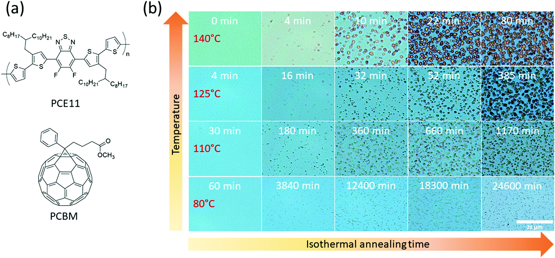 | ||
| Fig. 1 (a) Chemical structure of PCE11 and PCBM. (b) Optical micrographs of PCE11:PCBM films between isothermal annealing steps at 140, 125, 110 and 80 °C, indicated at left column. Total annealing time is indicated on the top of each micrograph. The scale bar (20 μm) is equal for all micrographs. | ||
Results
To study the thermal phase evolution of PCE11:PCBM BHJ, we selected a blend ratio of 1![[thin space (1/6-em)]](https://www.rsc.org/images/entities/char_2009.gif) :1.2 w:w and film thickness of 300 nm because such films were reported to result in best OSC performance.42 To identify the time and temperature windows relevant for nano-to-macro-scale phase evolution, a film on quartz was isothermally step-wise annealed from room temperature to 160 °C. After each 5 min annealing step, the film was quenched to room temperature and its transmittance measured. Typical spectra are presented in Fig. S1a (ESI†). The transmittance at 800 nm, where there is no absorption by PCE11 or PCBM, is plotted as a function of annealing temperature in Fig. S1b (ESI†). Up to 135 °C the film transmittance remains constant at around 80%. Subsequent annealing at 140 °C results in a sharp decrease in the transmittance and after annealing at 145 °C the transmittance drops to ≈40%. Annealing at higher temperatures leads to a further gradual decrease. The decrease in the transmittance at 140 °C was previously associated with light scattering by growing PCBM aggregates.14,50 We deduce from Fig. S1b (ESI†) that the blend's Tg is just below 130 °C, in good agreement with the literature44 and estimation from the Fox equation (for details of Tg estimation refer to Section S1 in the ESI†). Therefore, annealing at temperatures well above 130 °C (i.e. above the Tg) allows high molecular mobility, while annealing far below Tg suppresses such mobility and hence we concentrate on temperatures close to the estimated Tg.
:1.2 w:w and film thickness of 300 nm because such films were reported to result in best OSC performance.42 To identify the time and temperature windows relevant for nano-to-macro-scale phase evolution, a film on quartz was isothermally step-wise annealed from room temperature to 160 °C. After each 5 min annealing step, the film was quenched to room temperature and its transmittance measured. Typical spectra are presented in Fig. S1a (ESI†). The transmittance at 800 nm, where there is no absorption by PCE11 or PCBM, is plotted as a function of annealing temperature in Fig. S1b (ESI†). Up to 135 °C the film transmittance remains constant at around 80%. Subsequent annealing at 140 °C results in a sharp decrease in the transmittance and after annealing at 145 °C the transmittance drops to ≈40%. Annealing at higher temperatures leads to a further gradual decrease. The decrease in the transmittance at 140 °C was previously associated with light scattering by growing PCBM aggregates.14,50 We deduce from Fig. S1b (ESI†) that the blend's Tg is just below 130 °C, in good agreement with the literature44 and estimation from the Fox equation (for details of Tg estimation refer to Section S1 in the ESI†). Therefore, annealing at temperatures well above 130 °C (i.e. above the Tg) allows high molecular mobility, while annealing far below Tg suppresses such mobility and hence we concentrate on temperatures close to the estimated Tg.
Optical microscopy
PCE11:PCBM BHJ films were annealed at 80 °C, 110 °C, 125 °C and 140 °C for varying times and periodically characterized by optical microscopy, as shown in Fig. 1b. The optical micrographs after all annealing treatments, including the relatively low 80 °C annealing temperature (compared to Tg), show distinct PCBM aggregates. However, at high annealing temperatures, e.g. 140 °C, the aggregates are distinguishable already after 4 min of annealing, while at 80 °C they are noticed much later, after 3840 min (Fig. 1b second column). The number of aggregates also depends on annealing temperature, with fewer aggregates observed in the initial stages of the higher annealing temperatures. For extended annealing times the number of apparent aggregates cannot be evaluated due to overlapping of adjacent aggregates. PCBM aggregates are larger as annealing temperature increases (≈2.6 μm2 after 80 min annealing at 140 °C compared to ≈1.1 μm2 after 84 min annealing at 125 °C and even smaller for 110 °C and 80 °C). These results are in a good agreement with the classical theory of nucleation and growth.45 High annealing temperatures enhance the diffusion of PCBM molecules leading to faster aggregate growth, accompanied with decrease of their number density, and in total to larger aggregates size.Spectroscopy
The aggregation of PCBM with time and temperature is also followed using optical absorption, as shown in Fig. 2. The spectra can be divided into two regions, below and above 390 nm, dominated by PCBM and PCE11 absorption, respectively (Fig. S2, ESI†). Annealing the blend film at low temperature, 80 °C, results in very minor changes in the spectrum even after an extended annealing period of 17 days (Fig. 2a). In contrast, annealing at temperatures close to the Tg results in extensive spectrum evolution (Fig. 2b–d). Intriguingly, the PCBM absorbance region (i.e. below 390 nm) decreases during the annealing process, while that of PCE11 (above 390 nm) increases. Earlier studies assigned this decrease in PCBM absorption to aggregation,51–53 which reduces the effective cross section for PCBM absorption. The increase in the PCE11 absorption region (above 390 nm) has two contributions, PCE11 absorption and scattering. The former is associated with the mobility and reorganization of the polymer chains during annealing.54,55 In particular, the intensity ratio between the 0–0 and 0–1 transitions (at 690 and 627 nm, respectively) gradually decreases from above 1 in the as cast films to below 1 during annealing at 110 °C, 125 °C and 140 °C. This reduction implies that upon annealing the chain packing shifts from J-type aggregation, usually associated with head-to-tail arrangement of polymer chains, to H-type aggregation, associated with side-by-side arrangement of polymer chains.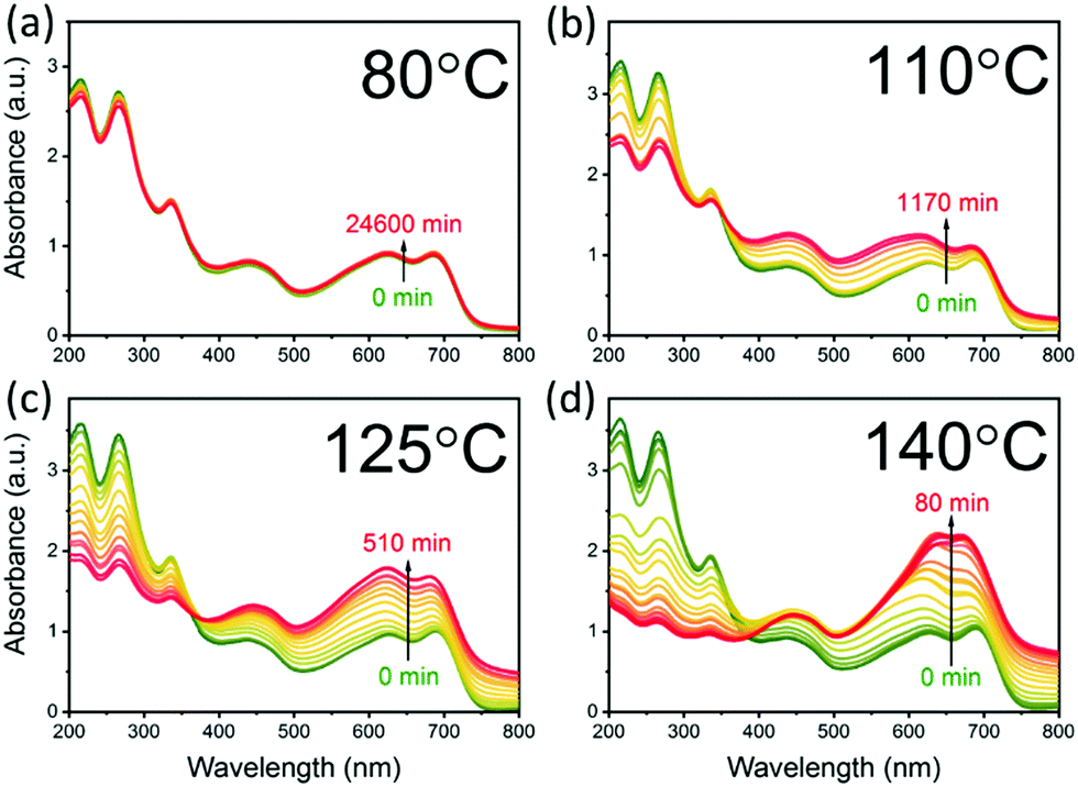 | ||
| Fig. 2 Optical absorption spectra of PCE11:PCBM films measured between isothermal annealing steps at (a) 80 °C, (b) 110 °C, (c) 125 °C and (d) 140 °C. Thermal annealing progress indicated by gradual change from green (non-annealed film) to yellow and to red (extended annealing time, indicated on each figure). | ||
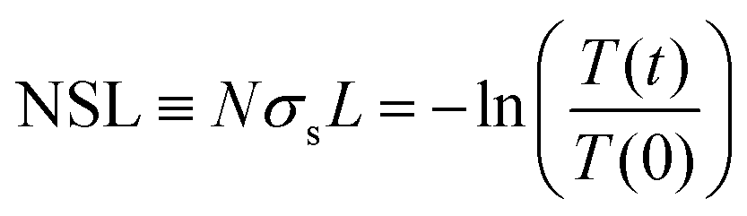
The contribution of light scattered by growing aggregates is noticeable mainly in the transparent region of the spectrum, ≈800 nm. Annealing at 80 and 110 °C has little effect on the spectrum in this region. On the other hand, progressive annealing at high temperatures, i.e. 125 °C and 140 °C (Fig. 2c and d, respectively), leads to a steady increase in light scattering apparent from the background-like trace at ≈800 nm. To quantitatively express the evolution of the scattering centers, we defined the following figure of merit:
 | (1) |
Fig. 3a shows the NSL evolution as a function of annealing time. Isothermal annealing at low temperature (80 °C) is characterized by a nearly constant NSL close to zero, as evident from the absorbance spectrum in Fig. 2a (not shown in Fig. 3a, but presented in Fig. S4 up to ≈17 days, ESI†). Annealing at 110 °C results in a moderate increase of the NSL after ≈20 hours. Annealing the films at higher temperatures (i.e. 125–140 °C), however, results in time-dependent sigmoidal curves suggesting the use of the JMAK equation (eqn (2)) to describe the temperature-dependent scattering evolution:21,56–59
| NSL(t) = NSL∞(1 − exp(−(kt)n)) | (2) |
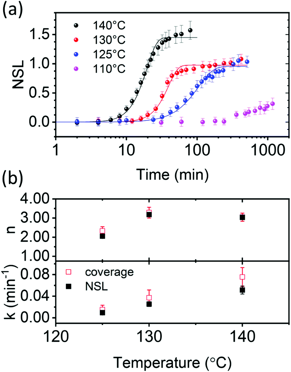 | ||
| Fig. 3 PCBM aggregate nucleation and growth kinetics in thermally annealed PCE11:PCBM films. (a) NSL as a function of annealing time at 140 °C (black), 130 °C (red), 125 °C (blue) and 110 °C (purple). Corresponding solid lines represent fits to the Avrami JMAK equation (eqn (2)) using Avrami exponent, n, and rate constant, k, extracted from Sharp–Hancock plots (eqn (S10), ESI†). (b) Comparing the Avrami parameters, n and k, extracted from Sharp–Hancock plots using either the NSL (black filled squares) or the PCBM aggregates coverage in optical micrographs in Fig. S4b (ESI,† red empty squares). | ||
The Avrami exponent values (n) and rate constants (k) were obtained from the Sharp–Hancock plots for the higher annealing temperatures (Fig. 3b). The exponent values (n) at the higher temperatures (130 and 140 °C) are close to 3 (Fig. 3b), which is consistent with either an interface mobility-controlled growth with heterogeneous nucleation, or a diffusion limited growth with increasing nucleation rate.45,57,60 The extracted rate constants (k) are used to plot Arrhenius curves, logk as a function of 1/T, to estimate the activation energy for PCBM aggregation (Fig. S6, ESI†). The calculated activation energy, 1.32 ± 0.4 eV, is similar to the value reported for poly(3-hexylthiophene) (P3HT):PCBM blends, 1–1.5 eV, which was assigned to PCBM aggregation by coalescence of PCBM crystallites in a diffusion-limited process.61 Therefore, based on the literature for P3HT:PCBM and the high activation energy found here, we speculate that PCBM aggregate growth in PCE11:PCBM BHJs during annealing in the 125–140 °C temperature range is also diffusion limited. It should be noted that the energy barrier for the nucleation of the crystalline PCBM phase also contributes to the activation energy for k.
To validate our speculation we compared the NSL figure of merit, to the area covered by PCBM aggregates in the optical micrographs, as a function of time and temperature (Fig. 1b). Assuming the NSL value represents the total scattering cross section in each sample, and not sensitive to issues such as aggregate shape, size and surface texture, then it can be compared to the area covered by the aggregates. Indeed, PCBM-covered area in each optical micrograph taken between isothermal annealing steps also yielded sigmoidal curves similar to the Avrami plots (Fig. S4b, ESI†). Therefore, we fitted the Sharp–Hancock equation (eqn (S10), ESI†) also to the coverage-vs.-time curves in Fig. S4b (ESI†) and extracted the Avrami parameters. Fig. 3b compares the n and k parameters extracted from the scattering data (NSL) and the optical microscopy data (coverage). The exponent and rate constants extracted from both techniques agree within the error bars. Moreover, the activation energy for PCBM aggregation, calculated from the slope of the Arrhenius plots using the rate constants obtained from the optical microscopy data, Fig. S6 (ESI†), is similar to that calculated form the NSL data, 1.31 ± 0.3 eV. This agreement between both techniques validates the use of NSL as a figure of merit to describe the evaluation of PCBM aggregation kinetics, and confirms that PCBM aggregation during annealing in the 125–140 °C range is diffusion limited.61,62
Vapor phase infiltration (VPI)
In the sections above, light scattering and optical microscopy were successfully used to follow the micro-scale PCBM aggregation growth kinetics. However, PCBM nucleation and growth on the nano-scale are below the detection threshold of these techniques (ca. 400 nm). Therefore, to follow the initial stages of PCBM aggregation we performed the VPI processes on thin films annealed for 12 min at different temperatures. In the VPI process, the films are exposed to alternating cycles of ZnO precursors, diethylzinc and water, at 60 °C. The precursors diffuse and reside preferably in PCE11-rich regions, resulting in selective deposition of ZnO inside these domains. Under such conditions, the ZnO can be used as a contrast agent in electron microscopy and effectively map the distribution of PCE11-rich domains in the BHJ. Namely, regions with ZnO, i.e.PCE11-rich domains, will appear bright in cross section high-resolution scanning electron microscopy (HRSEM) BSE detector imaging; while regions with no ZnO, i.e.PCBM-rich domains, will appear dark.37Cross-section HRSEM micrographs of films annealed for 12 min and then processed in VPI, Fig. 4, clearly show the evolution of PCBM aggregates through all annealing temperatures. More specifically, annealing at 110 °C (Fig. 4a) leads to bicontinuous phase separation with length scale of ≈0.2 μm; annealing at 130 °C (Fig. 4b) generates aggregates ≈0.5 μm in diameter; and after annealing at 150 °C (Fig. 4c) the PCBM aggregates are beyond 2 μm in diameter. The fine phase separation identified in all annealed films could not be characterized by optical microscopy, emphasizing the necessity and uniqueness of VPI for BHJ morphology characterization. The gradual growth of the PCBM aggregates with annealing temperature is consistent with the optical micrographs presented in Fig. 1b, and reflects the strong dependence of diffusion on temperature (Arrhenius behavior) which leads to a steep increase of growth rate with annealing temperature. Importantly, the image of the film annealed at 150 °C also reveals a surprising finding: presence of both a bicontinuous fine phase-separated morphology (marked by a yellow circle in Fig. 4c) and very large aggregates (>2 μm). These morphological features are generally mutually exclusive and their co-existence is striking and provides unprecedented information on the temperature-induced morphology evolution in this system. We will later suggest a model that bridges the thermodynamics and kinetics of temperature-induced PCBM aggregate growth in polymer:fullerene blends and explains this unusual observation.
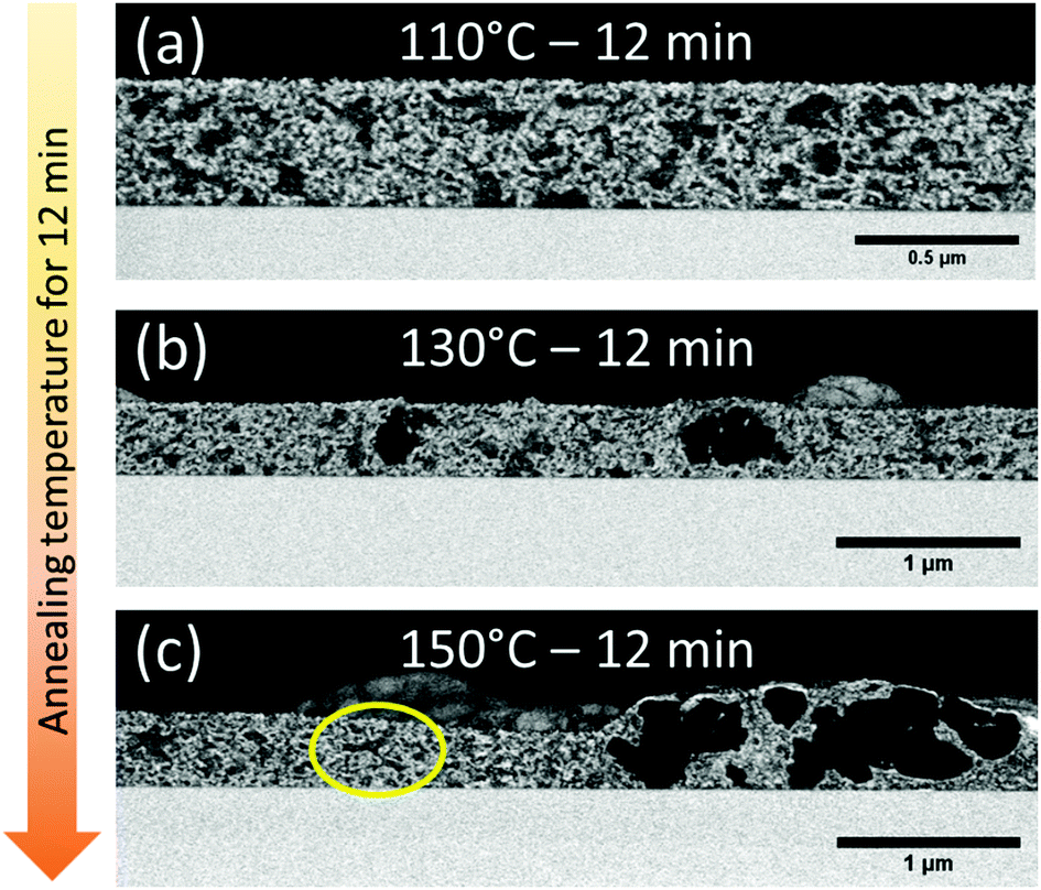 | ||
| Fig. 4 Cross-section HRSEM BSE micrographs of spin-coated PCE11:PCBM 1:1.2 w:w 300 nm thick films after thermal annealing for 12 min at various temperatures: (a) 110 °C, (b) 130 °C and (c) 150 °C. After annealing thin films were exposed to 20 cycles of DEZ and water at 60 °C. The bright contrast in the films represents areas with ZnO indicating a PCE11-rich phase, while the dark areas are all-organic domains corresponding to the PCBM-rich phase. The yellow circle in (c) indicates the fine bicontinuous phase separation present in the film even after annealing at 150 °C. | ||
We now use VPI to closely follow the initial stages of PCBM aggregation. To do so, PCE11:PCBM films were annealed at an intermediate temperature, 130 °C, for various time periods between 2 and 90 min, and then exposed to the VPI process. The cross-section HRSEM image of the VPI-treated as-cast film, Fig. 5a, shows a homogeneous morphology composed of visible gray/bright <0.1 μm bicontinuous phase separation. This morphology is typical of spinodal decomposition, which is in good agreement with theoretical studies of PCE11:PCBM blends conducted by Perea et al.8,22 The dim contrast of the PCBM-rich gray domains is probably due to some (bright) ZnO deposition inside generally dark-contrast PCBM domains. This suggests that the PCBM domains also include some PCE11. The bright regions, on the hand, include both polymer-rich domains and domains of a mixed phase that contains a significant amount of PCBM. We therefore find, in agreement with earlier studies, that the as-cast film consists of three types of domains: PCBM-rich domains (dim gray), a polymer-rich phase (bright) and a mixed phase (bright), phase separated on a <0.1 μm length scale.8,26,63–66
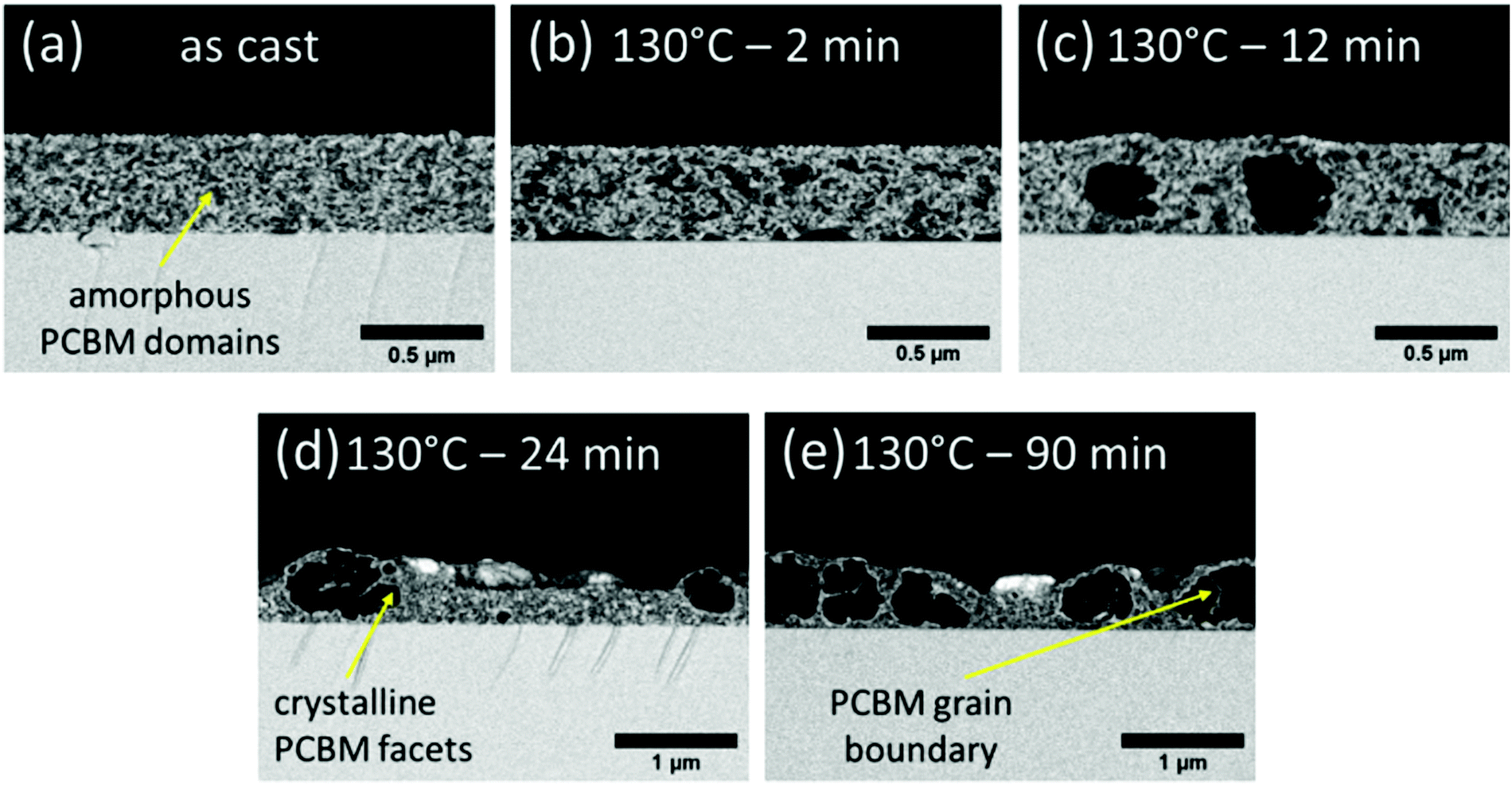 | ||
| Fig. 5 Cross-section HRSEM BSE micrographs of PCE11:PCBM films after thermal annealing at 130 °C for various time periods and VPI: (a) 0 min (as cast), (b) 2 min, (c) 12 min, (d) 24 min and (e) 90 min. After annealing, the films were exposed to a VPI process of 20 DEZ and water cycles at 60 °C. The bright contrast in the films represents areas with ZnO indicating a PCE11-rich phase, while the dark areas are all-organic domains corresponding to the PCBM-rich phase. The gray scale of the Si substrate is similar in all images and used as a reference to compare contrast and brightness in the micrographs. | ||
Annealing at 130 °C for 2 min leads to a slight increase in the length scale of phase separation and stronger bright/dark contrast (Fig. 5b). The stronger contrast is a result of the darker appearance of the PCBM domains in the annealed films, compared to the grey shade in the as-cast film, indicating an increase of PCBM content in these domains. The growth of the PCBM domains during the annealing process is at the expense of the mixed phase leaving behind a PCE11-rich phase. Annealing for longer, i.e. 12 min (Fig. 5c), results in morphology coarsening, characterized by large (>300 nm), nearly spherical PCBM aggregates. Further annealing results in even more coarsening, aggregate growth beyond film thickness and eventually particles extending over a micron (Fig. 5d and e) with few smaller scale aggregates, ∼200 nm (in the middle of Fig. 5d). The size and abundance of these large aggregates is in agreement with those observed in the optical microscopy images of films annealed at similar temperatures for similar time periods (Fig. 1b).
Photoluminescence
To corroborate the observed donor:acceptor phase demixing and separation during annealing we carried out PL experiments on a similar series of samples, i.e. BHJs annealed at 130 °C for varying time periods. Generally, PL quenching by exciton dissociation is significantly suppressed when donor–acceptor phase separation is larger than the exciton diffusion length (tens of nm).22,67Fig. 6a shows the PL spectra of the films corrected for scattering background and absorption intensity. The PL signal of the as-cast film (0 min) is nearly fully quenched, corresponding to a morphology where PCE11 and PCBM molecules are in close proximity sufficient to dissociate of the photoexcitation. Annealing at 130 °C leads to an increase of the PL signal with the intensity generally increasing with annealing time. We assign this increase in PL intensity to coarsening of the PCBM-rich and PCE11-rich phases, as observed in the HRSEM images of Fig. 5. After 40 min of annealing, the PL signal saturates indicating that the nm-scale phase separation that caused quenching no longer exists, and suggesting that at this stage the PCE11-rich phase already reached its equilibrium composition.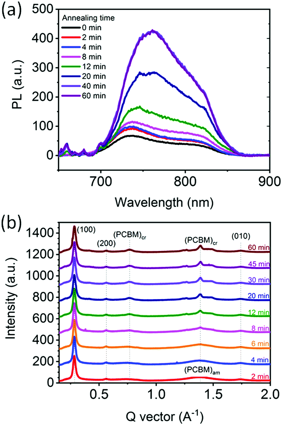 | ||
| Fig. 6 Microstructure characterization of PCE11:PCBM films. (a) Photoluminescence spectra of as-cast and films annealed at 130 °C for 2 to 60 min. PL spectra was corrected for scattering background and absorption intensity (for raw data see Fig. S7, ESI†). (b) 1-D scattering profiles of 2D GIWAXS collected in situ during isothermal annealing at 130 °C at various annealing times (indicated on the figure). The data have been shifted for clarity. Representative GIWAXS scattering images shown in Fig. S8 (ESI†). The peaks at q ∼ 0.28 Å−1, q ∼ 0.56 Å−1, 0.83 Å−1 and q ∼ 1.74 Å−1 correspond to (100), (200), (300) and (010) reflections of PCE11. The peaks at q ∼ 0.77 Å−1 and q ∼ 1.39 Å−1 belong to crystalline PCBM. | ||
Grazing incidence wide-angle X-ray scattering (GIWAX)
The phase evolution is also followed using in situ GIWAXS measurements that probe the crystallinity evolution of PCBM in PCE11:PCBM thin film during annealing at 130 °C (Fig. 6b). Strong (100), (200), (300) and (010) peaks of PCE11 are evident throughout the annealing process confirming the presence of semi-crystalline PCE11 from film deposition. Here we use (100) and (010) to denote lamella and pi-stacking directions and planes. In contrast, PCBM domains are amorphous in the first 6 min of annealing, evident from the broad halo features at ∼0.75 Å−1 and q ∼ 1.39 Å−1 (Fig. S8a, ESI†). After 6 min of annealing two sharp features emerge at q ∼ 0.77 Å−1 and q ∼ 1.39 Å−1 demonstrating the presence of PCBM crystallites.68 The crystalline PCBM peaks remain azimuthally isotropic in intensity (Fig. S8, ESI†), showing that PCBM crystallites are randomly oriented supporting the 3D growth regime. The area of these peaks in the corresponding 1-D scattering profiles (Fig. 6b) increases with annealing time at the expense of amorphous PCBM showing further crystallization of PCBM. The crystal coherence length (CCL), commonly used as a proxy for the size of the crystalline domains with all other morphological features being equal,69 and crystalline PCBM peak area are extracted from the background corrected 1.39 Å−1 peak and presented in Fig. S9 (ESI†). The 3rd power of the CCL and the peak area follow a very similar trend suggesting that the overall increase of PCBM crystallinity is predominantly due to the growth of already present crystals and not due to the nucleation of new ones.70 Both also increase gradually with annealing time and saturate after 30 min, indicating that after 30 min the present PCBM crystals stop growing. At the same time, the halo features corresponding to amorphous PCBM have largely disappeared. The apparent correlation between the time the PL signal and the PCBM crystallization saturation (30–40 min) indicates that the crystallization process ceases at the same time the fine phase separation disappears, suggesting that the crystallization of PCBM is on expense of the fine phase separated morphology.After following the initial stages of the morphology evolution with PL, GIWAXS, VPI and HSREM, and the later stages with optical microscopy and spectroscopy, we now combine the insights to understand the mechanism. The optical microscopy and scattering results revealed that PCBM aggregate growth follows the JMAK equation indicating that PCBM aggregation is due to a heterogeneous transformation process, i.e., through nucleation and then growth. On the other hand, the HRSEM images revealed that the initial film morphology appears to be associated with a bicontinuous spinodal-like phase separation morphology, which would suggest a homogeneous transformation, i.e. a spontaneous phase separation with no nucleation stage (spinodal decomposition). These two mechanisms, spinodal decomposition vs. nucleation and growth, are mutually exclusive and their co-existence would be extraordinary because thermodynamics dictates that binary systems can evolve only through one of these mechanisms.71
We offer here a model that bridges the thermodynamics and kinetics of the temperature-induced morphology evolution in PCE11:PCBM, and propose that both mechanisms can occur in this system, but apply to two distinct transformations. More specifically, we suggest that the initial stages of the morphology evolution can go through spinodal decomposition that leads to the demixing of the mixed phase. However, once the PCBM-rich domains with a composition corresponding to a metastable state are formed, morphology evolution is dominated by the nucleation of the PCBM crystals and their aggregation into polycrystalline aggregates.
Discussion
We start the discussion of the phase evolution from the solution where the donor, acceptor and solvent molecules are fully intermixed. The BHJ morphology of the as-cast film is formed during the spin coating deposition process while the solvent molecules evaporate and the cooling terminates. We speculate that the fast solvent evaporation quenches the solution from the single-phase region into the unstable part of the ternary (PCE11–PCBM–DCB) phase diagram. Few theoretical studies demonstrated spinodal demixing during drying and indeed the image in Fig. 5a shows indications of some spinodal decomposition microstructure.72,73 However, the fast solvent evaporation and cooling rates also lead to a rapid increase in solution viscosity and halt of solute mass transport affectively “freezing” the system in a kinetically-trapped morphology. “Freezing” the spinodal decomposition in course leads to PCBM-rich domains, polymer-rich domains and mixed-phase domains, as seen in the image of the as-cast film in Fig. 5a. Presence of the mixed phase is evident from the strong PL quenching (black line in Fig. 6a) and the dim contrast in the VPI image (Fig. 5a); while the GIWAXS data indicates that the PCBM domains are amorphous.The “kinetically-trapped” morphology is the starting point for the annealing process and hence, instead of the equilibrium PCE11:PCBM phase diagram, the analysis of the microstructure evolution should be described by its metastable counterpart that describes the metastable phase equilibria of PCBM-rich crystalline phase with PCE11:PCBM mixed phase (denoted as M2 in Fig. 7a). We propose that this metastable diagram is of a monotectic type, similarly to that of the PffBT4T-2DT:O-IDTBR system recently described by Hamid et al.74 The kinetic “freeze-in” to room temperature, i.e. below the monotectic temperature effectively quenches the blend into the unstable part of this metastable phase diagram (spinodal region). In this region, the system undergoes a spontaneous and homogeneous phase separation, i.e. spinodal decomposition (see Fig. 5b, and the green horizontal line in Fig. 7a). This observation is consistent with previous studies that correlated the strong burn-in degradation of highly efficient solar cells, including PCE11:PCBM, with spinodal donor–acceptor demixing.8,22,73
 | ||
| Fig. 7 The suggested microstructure evolution mechanism. (a) The suggested metastable PCE11:PCBM phase diagram. M, M1 and M2 denote the PCE11:PCBM mixed phase with different compositions, APCBM is the amorphous PCBM-rich phase, and CPCBM and CPCE11 are the semi-crystalline PCBM-rich and PCE11-rich phases, respectively. The blue arrow indicates the “kinetic freeze-in” during film deposition. Annealing the amorphous PCE11:PCBM blend of the composition corresponding to the spinodal region of the metastable liquid–liquid miscibility gap results in spinodal decomposition and formation of a bicontinuous microstructure (green horizontal line). The PCBM-rich domains eventually reach the composition of the metastable extension of the “crystalline PCBM-liquid” liquidus line, enabling the nucleation and growth of PCBM crystallites within the PCBM-rich domains (black arrow pointing to the left). The supersaturation of the PCBM-rich domain, Δ, determining the driving force for the nucleation of the PCBM is marked by a brown section. (b) Schematic illustration of microstructure development under thermal annealing. | ||
Thermal annealing enhances the diffusion of PCBM molecules from the mixed PCE11:PCBM phase towards the initially phase-separated PCBM domains slowly depleting the mixed phase (Fig. 5b). In parallel and due to the spinodal decomposition, PCBM molecules aggregate also inside the mixed phase (as illustrated at Fig. 7b). The combination of these processes causes the mixed PCE11:PCBM phase to separate into PCE11-rich and PCBM-rich phases leading to a steep decrease in PCBM–PCE11 interfacial area. The reduction of interfacial area is evident in the increase of the PL signal, as observed in Fig. 6a. The PCBM aggregates grow with time until they reach the critical radius and composition enabling heterogeneous nucleation of the crystalline phase (black horizontal arrow in Fig. 7a). Indeed, the critical radius for PCBM crystallization, although in P3HT, was previously calculated to be only few nm (roughly 7–19 nm).62 The GIWAXS results in Fig. 6b confirm the early crystallization of PCBM showing presence of PCBM crystals already after 6 min of annealing (Fig. 6b and illustration in Fig. 7b).
The particle size (Fig. 5), degree of crystallinity and CCL3 (Fig. S9, ESI†) continue to increase with annealing time. A close look at the large PCBM particles also reveals presence of faceted grain boundaries inside the aggregates (arrow in Fig. 5e). The grain boundaries can be recognized by thin bright stripes, which are platelets of ZnO. We suggest that PCE11 “wets” the grain boundaries allowing VPI precursor diffusion and ZnO deposition in the grain boundaries, leading to their “staining” and broadening. In-particle grain boundaries generally indicate coarsening through attachment of smaller crystalline aggregates. Therefore, the images reveal that the large PCBM particles are actually aggregates of PCBM crystallites coalesced into micron-size polycrystalline particles.
Employing the proposed metastable PCE11:PCBM phase diagram (Fig. 7a) offers the explanation to the morphology evolution and the formation of the crystalline PCBM particles. Indeed, the proposed diagram resolves the co-existence of the mutually exclusive transformation processes, i.e. spinodal decomposition vs. nucleation and growth. As shown above, spinodal decomposition occurs due to quenching the PCE11:PCBM blend into the unstable area of the phase diagram leading to spontaneous and homogeneous separation into PCE11-rich and PCBM-rich domains. At this stage, however, there is no thermodynamic driving force for the nucleation of the crystalline PCBM particles from the PCBM-rich domains. Such driving force only appears once the composition of the PCBM-rich domains reaches the metastable (i.e. below the monotectic temperature) extension of the “crystalline PCBM-liquid” liquidus line (in the context of the phase diagram, liquid phases refer to amorphous phases, here it specifically means the mixed phase). At this stage, the nucleation of the crystalline PCBM precipitates inside the PCBM-rich amorphous domains becomes possible. This nucleation is associated with the nucleation barrier which depends on the driving force for nucleation and the energy of the interface between the crystalline and amorphous PCBM phases, and which is unrelated to the activation energy for diffusion of individual PCBM molecules. The proposed scenario is consistent with the JMAK analysis of the overall growth kinetics of the relative amount of the crystalline PCBM phase (see Fig. 3). Indeed, the obtained value of the Avrami exponent (n = 3) is consistent with the diffusion-controlled nuclei growth and an increasing nucleation rate of the crystalline PCBM phase. In this case, the activation energy for the rate constant k is a convolution of the activation energy for the nuclei growth (presumably controlled by diffusion of the individual PCBM molecules), and the energy barrier for nucleation. The latter can be comparable to the former, resulting in high activation energy for the constant k, in agreement with the values calculated from Arrhenius plots of the NSL and optical microscopy results.
As for the polycrystalline nature of the PCBM aggregates, two possible reasons for their formation can be considered.
(1) Coalescence of the neighboring growing single crystalline PCBM particles, similarly to the formation of polycrystalline metals during solidification from the melt. We feel that this natural reason does not provide a complete description of the phenomenon, since the microstructure at the late stages of annealing features very large, and well-separated polycrystalline aggregates (see Fig. 5d and e).
(2) Brownian motion and coalescence of the growing single crystalline PCBM particles. This mechanism should be especially important at the initial stages of transformation, when the PCBM crystallites are still sufficiently small for rapid diffusion. This is because the mobility of Brownian particles scales inversely with their diameter, and the corresponding motion becomes significant for the particles smaller than 1 μm in diameter.75 We believe that, in practice, a combination of the two mechanisms considered above is responsible for the formation of the polycrystalline PCBM aggregates.
Comparing the HRSEM images of BHJs annealed at 130 and 150 °C (Fig. 5 and 4c, respectively) provides the final evidence corroborating the suggested mechanism. The series of images in Fig. 5 shows that the fine bicontinuous phase separation observed in the first few minutes of annealing at 130 °C eventually completely disappears, and is replaced by large coarse PCBM aggregates. In contrast, large aggregates and fine bicontinuous phase-separated morphology coexist in the film annealed at 150 °C (Fig. 4c). The source of this difference is in the dissimilar dependence of the nucleation and the growth rates on temperature.76 Nucleation in a solid–solid transformation is a competition between the thermodynamic driving force for nucleation of a more stable phase and the energy of the matrix–nucleus interface. While the latter only weakly depends on temperature, the former is a strong function of undercooling/super-saturation. In the present case, the driving force for nucleation of the crystalline PCBM phase scales with the distance between the metastable extensions of the liquidus and liquid–liquid separation lines (brown section in Fig. 7). The temperature of 150 °C is closer to the metastable monotectic temperature and, hence, the driving force for nucleation of the crystalline PCBM phase at this temperature is smaller than that at 130 °C. Since the energy barrier for nucleation scales inversely with the square of the driving force, this barrier should be much higher at 150 °C than at 130 °C. As a result, the nucleation rate at 150 °C is much smaller than that at 130 °C, which results in fewer large PCBM particles in the film annealed at 150 °C, with the regions of untransformed spinodal microstructure in-between. Hence, after 12 min of annealing at 150 °C large crystalline PCBM aggregates (few micrometers in size) are already formed, while at the same time a bicontinuous spinodal-like phase separation is still present, due to the low nucleation rate of the crystalline PCBM. Importantly, it should be noted that spinodal decomposition of PCE11:PCBM in the early stages of the morphology evolution was theoretically studied in a thermodynamic framework by Perea et al.22 In parallel, Berriman et al. suggested that PCBM aggregation in P3HT:PCBM blends is due to aggregation of PCBM crystallites ∼50 nm in size.62 The mechanism we proposed here bridges between the thermodynamic considerations discussed by Perea et al. and the kinetic results and model reported by Berriman, and provides new insights onto the of temperature-induced morphology evolution in BHJs.
Finally, we harness the insights gained on thermal morphology evolution to study the morphology-performance correlation in corresponding PCE11:PCBM OSCs. To do so we prepared a series of PCE11:PCBM OSCs and thermally annealed them at 130 °C for various times between 1 and 120 min (for device structure see Fig. S10a, ESI†). The device performance and photovoltaic parameters as a function of annealing time are presented in Fig. S10b (ESI†) and Fig. 8, respectively (the measured values are tabulated in Table S1, ESI†). Fig. 8 shows that the as-prepared device has the highest photovoltaic parameters and thermal annealing generally degrades the device. The first very short annealing treatment, <1 min (orange region in Fig. 8), leads to a significant parameter fall-off where the PCE drops by more than 40%, mainly due to a decrease of short circuit current (Jsc) by ∼30%. The fill factor (FF) and open circuit voltage (Voc) decrease by roughly 10%. This initial reduction is followed by a recovery of all parameters during the next 1–6 annealing min (green region in Fig. 8), yet recovery is not complete (∼85%, ∼95% and ∼80% for Jsc, FF (and Voc) and PCE, respectively). Further annealing induces fast degradation during a period of about 30 min (purple region in Fig. 8), mainly of the generated photocurrent and hence also the PCE. After the fast degradation stage, the devices continue to degrade, but albeit at significantly slower rate (blue region in Fig. 8).
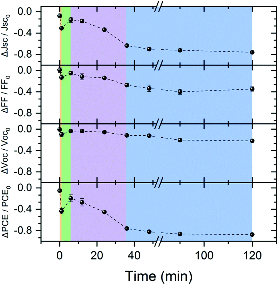 | ||
| Fig. 8 PCE11:PCBM OSC photovoltaic parameters: normalized Jsc, FF, Voc, and PCE as function of annealing time at 130 °C extracted from the J–V curves (Fig. S10, ESI†). The data is normalized with respect to the value measured on the same device before the annealing treatment, in order to minimize the deviations between devices that could be introduced in the preparation process. The dashed lines guide the eye. The background color represents four distinct time zones: orange (<1 min) where there is a sharp decrease in device parameters; green (1–6 min) parameter recovery; purple (6–36 min) with fast degradation; and blue (>36 min) slow performance degradation. | ||
We can now use the model we developed for the thermally-induced morphology evolution to explain each degradation step and correlate the device performance with film morphology. As mentioned earlier, film deposition generates a BHJ consistent of crystalline PCE11 domains, amorphous PCBM domains and an intimately mixed phase. In the as – cast film, therefore, excitons generated in the mixed phase can dissociate into charge carriers due to the high donor–acceptor interface area. Electrons that reach PCBM-rich domains and holes that reach crystalline PCE11 domains can percolate along interconnected networks to the electrodes. In the first minute of annealing (orange region in Fig. 8), the film undergoes rapid demixing where small PCBM particles are formed on expense of the mixed molecules. The significant decrease in donor–acceptor interfacial area dramatically reduces the generated photocurrent, evident from the 30% decrease in Jsc and significant increase in PL (Fig. 6a). Moreover, the small PCBM particles do not provide a sufficient percolation path to the electrodes. The stranded excitons enhance bimolecular recombination, as reflected in the 10% drop in both Voc and FF.77,78 Also, the ongoing spinodal decomposition in remaining mixed phase further decreases the initial donor–acceptor interface area. In the next few minutes of annealing (up to 6 minutes), PCBM demixing continues while increasing the size and molecular ordering of the particles effectively reaching percolation threshold and reducing the recombination probability, eventually resulting in recovery of the photovoltaic parameters (green region in Fig. 8). The next annealing stage, 6–36 minutes, corresponds to the time zone of nucleation and growth of the PCBM polycrystalline aggregates in the JMAK curves (Fig. 3a). The coarsening of the BHJ morphology by diffusion collisions and/or Brownian motion and agglomeration of PCBM crystallites to form the large aggregates rapidly and critically reduces the donor–acceptor interfacial area leading to a sharp and persistent loss of the photovoltaic performances (purple area in Fig. 8). Finally, after 36 min, the PCE11-rich matrix reaches its equilibrium composition, evident for the PL and GIWAXS in Fig. 6, demixing of PCBM ceases, and the fine structure disappears, as evident from the HRSEM images in Fig. 5. Although coarsening continues at this stage, it involves the coalescence of very large, slowly moving PCBM particles. This coarsening does not lead to significant changes in donor–acceptor interfacial area or morphologies that are device-relevant, resulting in a slow monotonous decrease of the photovoltaic parameters (blue region in Fig. 7). Additionally, an organic/electrode interface roughness, induced by large aggregates after extended annealing times, may also contribute to the overall performance degradation.
Conclusions
In this work we studied the temperature-induced BHJ morphology evolution of a high efficiency OSC blend, PCE11:PCBM, through a series of thermal annealing treatments. We observe in this system the two mutually exclusive phase transformation mechanisms: spinodal decomposition and nucleation and growth. This extraordinary finding reveals that the morphology evolution of this blend during annealing goes through two distinct and consecutive transformation processes. The initial stages of the morphology evolution of the film are governed by spontaneous and homogeneous spinodal decomposition, in accordance with the liquid–liquid miscibility gap in the metastable monotectic PCE11:PCBM phase diagram. We believe that this metastable phase diagram is more relevant for the system studied in the present work than the equilibrium diagram because the rapid solvent evaporation results in a “kinetically-trapped” morphology. The inherently low miscibility in this system leads also to some minor phase separation of amorphous PCBM domains during the fast solvent evaporation. The later stage of the morphology evolution, after the crystallization of PCBM, is governed by the nucleation and growth of stable monocrystalline PCBM aggregates from the PCBM-rich spinodal domains. These aggregates are formed through the collisions of neighboring growing PCBM crystallites, and through their Brownian motion and agglomeration, and are polycrystalline in nature. Finally, the proposed mechanism allowed us to correlate the temperature-induced morphology evolution with the degradation of device parameters. This research demonstrates that while rapid solvent evaporation during film deposition invokes kinetic and thermodynamic considerations that determine the morphology of the as cast film, the following evolution processes can evolve through distinct kinetic pathways directed by mutually exclusive thermodynamic considerations. This unexpected evolution process is not limited to fullerene-based blends and could possibly occur in other low miscibility systems such as blends based on non-fullerene acceptors. Decoupling the thermodynamic and kinetic considerations during the advanced stages of annealing from those that direct the early morphology evolution is essential for understanding the thermal degradation processes towards the development of efficient and stable new OSC systems.Experimental
Materials
PCBM (purity 99.5%) was purchased from Nano-C. PCE11 (Mn ≈ 83 kg mol−1, D ≈ 2.15) was purchased from Ossila. DEZ packaged for use in deposition systems was purchased from Sigma-Aldrich. ZnO nanoparticle solution (Nanograde N10) was purchased from Nanograde. All materials were used as received.Thin film BHJ deposition
Si and Quartz substrates were sonicated in acetone, methanol and isopropanol for 15 min each. Substrates were blown dry with N2 gas and transferred in to an N2-filled glovebox for thin film deposition. Thin films were spin-coated form PCE11:PCBM 45:55 wt% solution (total concentration of 30 mg mL−1 in 1,2-dichlorobenzene). The solution was stirred at 130 °C for at least 3 h before spin coating. All substrates were heated to 130 °C immediately prior to deposition. Solution was spin coated at 800 rpm for 20 s followed by 4000 rpm for 2 s, to achieve 300 nm thick film (measured by a DektakXT profilometer and by cross section HRSEM imaging). Spin coated films were left to dry overnight inside the glovebox.
Organic solar cell fabrication
Devices were fabricated in inverted architecture: glass/ITO/ZnO/PCE11:PCBM BHJ/MoO3/Al. ITO-patterned glass substrates were sonicated in acetone, methanol and isopropanol for 15 min each and blown dry with N2 gas, followed by UV–ozone cleaning for 15 min. ZnO nanoparticle solution (Nanograde N10) was filtered through a 0.45 μm PTFE filter and sonicated for 5 min prior to deposition. ZnO nanoparticle hole blocking layers were spin coated onto the ITO substrates at 2500 rpm for 60 s, followed by thermal annealing at 120 °C for 5 min in ambient conditions. Thin film BHJs were spin coated inside the glovebox, as described above. For MoO3 electron blocking layer and Al anode deposition the devices were positioned in a thermal evaporator (inside the glovebox) at 10−6 mbar for 1 h, followed by deposition of 20 nm MoO3 and 100 nm Al. Thermal evaporation was conducted through a shadow mask resulting in effective device area of 0.03 cm2 (defined by the overlap area between the electrodes).Solar cells characterization
The solar cells characterization was performed under N2 atmosphere using a 100 mW cm−2 AM 1.5G Oriel Sol3A Newport Inc. solar simulator with a Keithley 2651A source meter.UV-vis absorption spectroscopy
UV-vis absorption spectra of the thin films on quartz substrates were measured with a Cary 100 scan UV-visible spectrophotometer.Optical microscopy
Optical micrographs were taken using a Zeiss Scope.A1 microscope equipped with a Zeiss AxioCam MRc 5 camera. The quantitative analysis of the micrographs was carried out using the Fiji image-analysis software.46Photoluminescence
PL spectra was measured using a Cary Eclipse Fluorescence Spectrophotometer. The thin films on quartz substrates were excited at 540 nm, while the emission spectra were collected in the 600–1000 nm range. The PL spectra were corrected by subtracting the background signal induced by scattering and normalizing for the absorbed intensity using the following equation:| PLcorr = PLmeasured/(1 − 10−A) |
Vapor phase infiltration
After film deposition, all samples were held for 8 h under 10−6 mbar vacuum for out-gazing solvent/moisture residues before the VPI process The VPI process was conducted in a Veeco Savannah S100 system. The Samples were exposed to 20 alternating cycles of DEZ and H2O at 60 °C. During each cycle, the samples were exposed to three DEZ pulses for 600 s, followed by a purge processes of 20 s, each time. After the DEZ pulses, the samples were exposed to three H2O pulses for 120 s each, followed by a purge processes of 120 s, each time. For more details on the VPI deposition of metal oxide inside organic matrices see ref. 40 and 41The VPI process condition were carefully adjusted to minimize morphology changes during process.
High-resolution scanning electron microscopy
Cross sections of the thin films on Si substrates were prepared by immersing the samples in liquid nitrogen, followed by cleaving. HRSEM micrographs were taken using a Zeiss Ultra-Plus FEG-SEM operated at 2 kV accelerating voltage with a working distance of ∼2.7 mm. Backscattered electrons signal (ESB detector) and secondary electrons signal (Inlens detector) were collected simultaneously.Grazing-incidence wide-angle X-ray scattering
GIWAXS images were collected with a 2D area X-ray detector (MX225, Rayonix, L.L.C.) with a pixel size of 73 μm (3072 × 3072 pixels) in a helium filled chamber at beamline 11-3 of the SSRL. The sample-to-detector distance was 340 mm, and the incidence angle was 0.14°; the X-ray wavelength was 0.9758 Å, corresponding to a X-ray beam energy of 12.735 keV. In situ GIWAXS measurements were recorded during annealing at 130 °C, controlled by an Omega Temperature Controller. The samples rose to and equilibrated at the desired annealing temperature within 30 s. Data was analyzed using the Nika package for Wavemetrics Igor software in combination with WAXS tools.48,49Conflicts of interest
There are no conflicts to declare.Acknowledgements
We thank Yonatan Markman and Noy Fabri for experimental assistance. This research was supported by the Israel Science Foundation (grant no. 283/16), and the United States-Israel Binational Science Foundation (BSF), Jerusalem, Israel. This research used beamline 11-3 at the Stanford Synchrotron Radiation Lightsource (SSRL). Use of SSRL, SLAC National Accelerator Laboratory, is supported by the U.S. Department of Energy, Office of Science, Office of Basic Energy Sciences under contract no. DE-AC02-76SF00515.Notes and references
- Q. Liu, Y. Jiang, K. Jin, J. Qin, J. Xu, W. Li, J. Xiong, J. Liu, Z. Xiao, K. Sun, S. Yang, X. Zhang and L. Ding, Sci. Bull., 2020, 65, 272–275 CrossRef CAS.
- K. A. Mazzio and C. K. Luscombe, Chem. Soc. Rev., 2015, 44, 78–90 RSC.
- B. C. Thompson and J. M. J. Fréchet, Angew. Chem., Int. Ed., 2008, 47, 58–77 CrossRef CAS.
- S. Günes, H. Neugebauer and N. S. Sariciftci, Chem. Rev., 2007, 107, 1324–1338 CrossRef.
- M. C. Scharber and N. S. Sariciftci, Prog. Polym. Sci., 2013, 38, 1929–1940 CrossRef CAS.
- Y. Huang, E. J. Kramer, A. J. Heeger and G. C. Bazan, Chem. Rev., 2014, 114, 7006–7043 CrossRef CAS.
- Y. Huang, E. J. Kramer, A. J. Heeger and G. C. Bazan, Chem. Rev., 2014, 114, 7006–7043 CrossRef CAS.
- N. Li, J. D. Perea, T. Kassar, M. Richter, T. Heumueller, G. J. Matt, Y. Hou, N. S. Güldal, H. Chen, S. Chen, S. Langner, M. Berlinghof, T. Unruh and C. J. Brabec, Nat. Commun., 2017, 8, 14541 CrossRef CAS.
- C. H. Peters, I. T. Sachs-Quintana, W. R. Mateker, T. Heumueller, J. Rivnay, R. Noriega, Z. M. Beiley, E. T. Hoke, A. Salleo and M. D. McGehee, Adv. Mater., 2012, 24, 663–668 CrossRef CAS.
- M. Jørgensen, K. Norrman, S. A. Gevorgyan, T. Tromholt, B. Andreasen and F. C. Krebs, Adv. Mater., 2012, 24, 580–612 CrossRef.
- P. Cheng and X. Zhan, Chem. Soc. Rev., 2016, 45, 2544–2582 RSC.
- A. Guerrero and G. Garcia-Belmonte, Nano–Micro Lett., 2017, 9, 10 CrossRef.
- S. Rafique, S. M. Abdullah, K. Sulaiman and M. Iwamoto, Renewable Sustainable Energy Rev., 2018, 84, 43–53 CrossRef.
- C. Lindqvist, A. Sanz-Velasco, E. Wang, O. Bäcke, S. Gustafsson, E. Olsson, M. R. Andersson and C. Müller, J. Mater. Chem. A, 2013, 1, 7174–7180 RSC.
- C. Müller, Chem. Mater., 2015, 27, 2740–2754 CrossRef.
- L. Duan, M. Guli, Y. Zhang, H. Yi, F. Haque and A. Uddin, Energy Technol., 2020, 1901401 CrossRef CAS.
- A. J. Pearson, T. Wang, R. A. L. Jones, D. G. Lidzey, P. A. Staniec, P. E. Hopkinson and A. M. Donald, Macromolecules, 2012, 45, 1499–1508 CrossRef CAS.
- L. Yu, D. Qian, S. Marina, F. A. A. Nugroho, A. Sharma, S. Hultmark, A. I. Hofmann, R. Kroon, J. Benduhn, D. M. Smilgies, K. Vandewal, M. R. Andersson, C. Langhammer, J. Martín, F. Gao and C. Müller, ACS Appl. Mater. Interfaces, 2019, 11, 21766–21774 CrossRef CAS.
- J. Jo, S.-S. Kim, S.-I. Na, B.-K. Yu and D.-Y. Kim, Adv. Funct. Mater., 2009, 19, 866–874 CrossRef CAS.
- J. J. Richards, A. H. Rice, R. D. Nelson, F. S. Kim, S. A. Jenekhe, C. K. Luscombe and D. C. Pozzo, Adv. Funct. Mater., 2013, 23, 514–522 CrossRef CAS.
- W. R. Wu, U. S. Jeng, C. J. Su, K. H. Wei, M. S. Su, M. Y. Chiu, C. Y. Chen, W. Bin Su, C. H. Su and A. C. Su, ACS Nano, 2011, 5, 6233–6243 CrossRef CAS.
- J. D. Perea, S. Langner, M. Salvador, B. Sanchez-Lengeling, N. Li, C. Zhang, G. Jarvas, J. Kontos, A. Dallos, A. Aspuru-Guzik and C. J. Brabec, J. Phys. Chem. C, 2017, 121, 18153–18161 CrossRef CAS.
- C. Lindqvist, J. Bergqvist, O. Bäcke, S. Gustafsson, E. Wang, E. Olsson, O. Inganäs, M. R. Andersson and C. Müller, Appl. Phys. Lett., 2014, 104, 153301 CrossRef.
- T. Wang, A. J. Pearson, A. D. F. Dunbar, P. A. Staniec, D. C. Watters, H. Yi, A. J. Ryan, R. A. L. Jones, A. Iraqi and D. G. Lidzey, Adv. Funct. Mater., 2012, 22, 1399–1408 CrossRef CAS.
- C. Zhang, T. Heumueller, S. Leon, W. Gruber, K. Burlafinger, X. Tang, J. D. Perea, I. Wabra, A. Hirsch, T. Unruh, N. Li and C. J. Brabec, Energy Environ. Sci., 2019, 12, 1078 RSC.
- C. Zhang, T. Heumueller, W. Gruber, O. Almora, X. Du, L. Ying, J. Chen, T. Unruh, Y. Cao, N. Li and C. J. Brabec, ACS Appl. Mater. Interfaces, 2019, 11, 18555–18563 CrossRef CAS.
- W. Zhang, R. Hu, X. Zeng, X. Su, Z. Chen, X. Zou, J. Peng, C. Zhang and A. Yartsev, Polymers, 2019, 11, 408 CrossRef.
- Y. Xin, G. Zeng, J. Y. Ouyang, X. Zhao and X. Yang, J. Mater. Chem. C, 2019, 7, 9513–9522 RSC.
- Q. Y. Li, J. Xiao, L. M. Tang, H. C. Wang, Z. Chen, Z. Yang, H. L. Yip and Y. X. Xu, Org. Electron., 2017, 44, 217–224 CrossRef CAS.
- B. Watts, W. J. Belcher, L. Thomsen, H. Ade and P. C. Dastoor, Macromolecules, 2009, 42, 8392–8397 CrossRef CAS.
- T. Wang, A. J. Pearson, A. D. F. Dunbar, P. A. Staniec, D. C. Watters, H. Yi, A. J. Ryan, R. A. L. Jones, A. Iraqi and D. G. Lidzey, Adv. Funct. Mater., 2012, 22, 1399–1408 CrossRef CAS.
- O. Bäcke, C. Lindqvist, A. Diaz De Zerio Mendaza, S. Gustafsson, E. Wang, M. R. Andersson, C. Müller and E. Olsson, Nanoscale, 2015, 7, 8451–8456 RSC.
- E. Verploegen, R. Mondal, C. J. Bettinger, S. Sok, M. F. Toney and Z. Bao, Adv. Funct. Mater., 2010, 20, 3519–3529 CrossRef CAS.
- S. Bertho, G. Janssen, T. J. Cleij, B. Conings, W. Moons, A. Gadisa, J. D’Haen, E. Goovaerts, L. Lutsen, J. Manca and D. Vanderzande, Sol. Energy Mater. Sol. Cells, 2008, 92, 753–760 CrossRef CAS.
- A. Swinnen, I. Haeldermans, M. Vande Ven, J. D’Haen, G. Vanhoyland, S. Aresu, M. D’Olieslaeger and J. Manca, Adv. Funct. Mater., 2006, 16, 760–765 CrossRef CAS.
- W. Chen, M. P. Nikiforov and S. B. Darling, Energy Environ. Sci., 2012, 5, 8045 Search PubMed.
- A. Levitsky, G. M. Matrone, A. Khirbat, I. Bargigia, X. Chu, O. Nahor, T. Segal-Peretz, A. J. Moulé, L. J. Richter, C. Silva, N. Stingelin and G. L. Frey, Adv. Sci., 2020, 2000960 CrossRef CAS.
- S. Obuchovsky, H. Frankenstein, J. Vinokur, A. K. Hailey, Y. L. Loo and G. L. Frey, Chem. Mater., 2016, 28, 2668–2676 CrossRef CAS.
- S. Obuchovsky, B. Shamieh, I. Deckman, G. Ankonina and G. L. Frey, Sol. Energy Mater. Sol. Cells, 2015, 143, 280–283 CrossRef CAS.
- S. Obuchovsky, M. Levin, A. Levitsky and G. L. Frey, Org. Electron., 2017, 49, 234–241 CrossRef CAS.
- C. Z. Leng and M. D. Losego, Mater. Horiz., 2017, 4, 747–771 RSC.
- Y. Liu, J. Zhao, Z. Li, C. Mu, W. Ma, H. Hu, K. Jiang, H. Lin, H. Ade and H. Yan, Nat. Commun., 2014, 5, 5293 CrossRef CAS.
- J. Zhao, Y. Li, G. Yang, K. Jiang, H. Lin, H. Ade, W. Ma and H. Yan, Nat. Energy, 2016, 1, 15027 CrossRef CAS.
- H. W. Ro, J. M. Downing, S. Engmann, A. A. Herzing, D. M. DeLongchamp, L. J. Richter, S. Mukherjee, H. Ade, M. Abdelsamie, L. K. Jagadamma, A. Amassian, Y. Liu and H. Yan, Energy Environ. Sci., 2016, 9, 2835–2846 RSC.
- J. W. Christian, The theory of transformations in metals and alloys, Pergamon, Amsterdam, 3rd edn, 2002 Search PubMed.
- J. Schindelin, I. Arganda-Carreras, E. Frise, V. Kaynig, M. Longair, T. Pietzsch, S. Preibisch, C. Rueden, S. Saalfeld, B. Schmid, J. Y. Tinevez, D. J. White, V. Hartenstein, K. Eliceiri, P. Tomancak and A. Cardona, Nat. Methods, 2012, 9, 676–682 CrossRef CAS.
- P. Westacott, N. D. Treat, J. Martin, J. H. Bannock, J. C. De Mello, M. Chabinyc, A. B. Sieval, J. J. Michels and N. Stingelin, J. Mater. Chem. A, 2017, 5, 2689–2700 RSC.
- J. Ilavsky, J. Appl. Crystallogr., 2012, 45, 324–328 CrossRef CAS.
- S. D. Oosterhout, V. Savikhin, J. Zhang, Y. Zhang, M. A. Burgers, S. R. Marder, G. C. Bazan and M. F. Toney, Chem. Mater., 2017, 29(7), 3062–3069 CrossRef CAS.
- C. Lindqvist, E. Wang, M. R. Andersson and C. Müller, Macromol. Chem. Phys., 2014, 215, 530–535 CrossRef CAS.
- H. W. Liu, D. Y. Chang, W. Y. Chiu, S. P. Rwei and L. Wang, J. Mater. Chem., 2012, 22, 15586–15591 RSC.
- M. Milanovich, T. Sarkar, Y. Popowski, J. Z. Low, L. M. Campos, S. Kenig, G. L. Frey and E. Amir, J. Mater. Chem. C, 2020, 8, 7698–7707 RSC.
- O. Oklobia and T. S. Shafai, Solid-State Electron., 2013, 87, 64–68 CrossRef CAS.
- F. C. Spano and C. Silva, Annu. Rev. Phys. Chem., 2014, 65, 477–500 CrossRef CAS.
- M. Li, A. H. Balawi, P. J. Leenaers, L. Ning, G. H. L. Heintges, T. Marszalek, W. Pisula, M. M. Wienk, S. C. J. Meskers, Y. Yi, F. Laquai and R. A. J. Janssen, Nat. Commun., 2019, 10, 1–11 CrossRef.
- N. Deb, R. R. Dasari, K. Moudgil, J. L. Hernandez, S. R. Marder, Y. Sun, A. Karim and D. G. Bucknall, J. Mater. Chem. A, 2015, 3, 21856–21863 RSC.
- J. L. Allen, T. R. Jow and J. Wolfenstine, Chem. Mater., 2007, 19, 2108–2111 CrossRef CAS.
- X. P. Wang, G. Corbel, S. Kodjikian, Q. F. Fang and P. Lacorre, J. Solid State Chem., 2006, 179, 3338–3346 CrossRef CAS.
- A. Sharenko, N. D. Treat, J. A. Love, M. F. Toney, N. Stingelin and T. Q. Nguyen, J. Mater. Chem. A, 2014, 2, 15717–15721 RSC.
- L. Yu, E. Davidson, A. Sharma, M. R. Andersson, R. Segalman and C. Müller, Chem. Mater., 2017, 29, 5654–5662 CrossRef CAS.
- G. A. Berriman, J. L. Holdsworth, X. Zhou, W. J. Belcher and P. C. Dastoor, AIP Adv., 2015, 5, 097220 CrossRef.
- G. A. Berriman, N. P. Holmes, J. L. Holdsworth, X. Zhou, W. J. Belcher and P. C. Dastoor, Org. Electron., 2016, 30, 12–17 CrossRef CAS.
- B. A. Collins, J. R. Tumbleston and H. Ade, J. Phys. Chem. Lett., 2011, 2, 3135–3145 CrossRef CAS.
- W. Yin and M. Dadmun, ACS Nano, 2011, 5, 4756–4768 CrossRef CAS.
- J. D. Roehling, K. J. Batenburg, F. B. Swain, A. J. Moulé and I. Arslan, Adv. Funct. Mater., 2013, 23, 2115–2122 CrossRef CAS.
- L. Ye, B. A. Collins, X. Jiao, J. Zhao, H. Yan and H. Ade, Adv. Energy Mater., 2018, 8, 1703058 Search PubMed.
- O. Todor-Boer, I. Petrovai, R. Tarcan, A. Vulpoi, L. David, S. Astilean and I. Botiz, Nanomaterials, 2019, 9, 1757 CrossRef CAS.
- E. Verploegen, C. E. Miller, K. Schmidt, Z. Bao and M. F. Toney, Chem. Mater., 2012, 24, 3923–3931 CrossRef CAS.
- J. Rivnay, S. C. B. Mannsfeld, C. E. Miller, A. Salleo and M. F. Toney, Chem. Rev., 2012, 112, 5488–5519 CrossRef CAS.
- A. Sharenko, M. Kuik, M. F. Toney and T.-Q. Nguyen, Adv. Funct. Mater., 2014, 24, 3543–3550 CrossRef CAS.
- F. S. Bates, Science, 1991, 251, 898–905 CrossRef CAS.
- C. Schaefer, J. J. Michels and P. Van Der Schoot, Macromolecules, 2016, 49, 6858–6870 CrossRef CAS.
- S. Kouijzer, J. J. Michels, M. Van Den Berg, V. S. Gevaerts, M. Turbiez, M. M. Wienk and R. A. J. Janssen, J. Am. Chem. Soc., 2013, 135, 12057–12067 CrossRef CAS.
- Z. Hamid, A. Wadsworth, E. Rezasoltani, S. Holliday, M. Azzouzi, M. Neophytou, A. A. Y. Guilbert, Y. Dong, M. S. Little, S. Mukherjee, A. A. Herzing, H. Bristow, R. J. Kline, D. M. DeLongchamp, A. A. Bakulin, J. R. Durrant, J. Nelson and I. McCulloch, Adv. Energy Mater., 2020, 10, 1903248 CrossRef CAS.
- A. Einstein, Ann. Phys., 1905, 322, 549–560 CrossRef.
- A. D. de Zerio and C. Müller, Adv. Energy Mater., 2018, 8, 1702741 CrossRef.
- G. Lakhwani, A. Rao and R. H. Friend, Annu. Rev. Phys. Chem., 2014, 65, 557–581 CrossRef CAS.
- B. Qi and J. Wang, J. Mater. Chem., 2012, 22, 24315–24325 RSC.
Footnote |
| † Electronic supplementary information (ESI) available. See DOI: 10.1039/d0mh01805h |
| This journal is © The Royal Society of Chemistry 2021 |