DOI:
10.1039/D0MH01588A
(Communication)
Mater. Horiz., 2021,
8, 276-283
A regioregular donor–acceptor copolymer allowing a high gain–bandwidth product to be obtained in photomultiplication-type organic photodiodes†
Received
5th October 2020
, Accepted 30th October 2020
First published on 31st October 2020
Abstract
Obtaining a photomultiplication-type organic photodiode with a high gain–bandwidth product is challenging. We show that a newly designed regioregular polymer enables the formation of a highly oriented face-on structure with a low trap density, leading to a high EQE and a fast response time. As a result, a gain–bandwidth product of over 4 × 10⁵ Hz is achieved.
New concepts
The gain and bandwidth of a photomultiplication-type organic photodiode (PM-OPD) have been observed to have a tradeoff relation; therefore, achieving a high gain–bandwidth product is technically limited. In this study, we show that the transient response of a PM-OPD can be artificially engineered based on a newly designed and synthesized regioregular polymer donor, poly[4,8-bis(5-(2-hexyldecyl)thiophen-2-yl)benzo[1,2-b![[thin space (1/6-em)]](https://www.rsc.org/images/entities/char_2009.gif) :4,5-b′]dithiophene] [5,5′-bis(7-(4-(2-butyloctyl)thiophen-2-yl)-6-fluorobenzo[c][1,2,5]thiadiazol-4-yl)-2,2′-bithiophene] (PDBD-FBT). We show that the regioregular nature of PDBD-FBT enables the formation of a highly oriented face-on structure, providing a low trap density in PM-OPDs, as confirmed by thermal admittance spectroscopy analysis. When a PM-OPD is constructed with PDBD-FBT by blending with 1 wt% ITIC, a high external quantum efficiency exceeding 60000% is achieved while a fast response time is maintained with a –3 dB cutoff frequency of ∼740 Hz, leading to a gain–bandwidth product of more than 4 × 10⁵ Hz and a high specific detectivity of 3.82 × 10¹² Jones. To demonstrate the feasibility of the fabricated PM-OPD with a high operation speed, a blood pulse measurement was performed. This study shows that response time and gain do not form a direct tradeoff relation in PM-OPDs, and a molecular approach can open the possibility of a fast temporal response with a high gain. :4,5-b′]dithiophene] [5,5′-bis(7-(4-(2-butyloctyl)thiophen-2-yl)-6-fluorobenzo[c][1,2,5]thiadiazol-4-yl)-2,2′-bithiophene] (PDBD-FBT). We show that the regioregular nature of PDBD-FBT enables the formation of a highly oriented face-on structure, providing a low trap density in PM-OPDs, as confirmed by thermal admittance spectroscopy analysis. When a PM-OPD is constructed with PDBD-FBT by blending with 1 wt% ITIC, a high external quantum efficiency exceeding 60000% is achieved while a fast response time is maintained with a –3 dB cutoff frequency of ∼740 Hz, leading to a gain–bandwidth product of more than 4 × 10⁵ Hz and a high specific detectivity of 3.82 × 10¹² Jones. To demonstrate the feasibility of the fabricated PM-OPD with a high operation speed, a blood pulse measurement was performed. This study shows that response time and gain do not form a direct tradeoff relation in PM-OPDs, and a molecular approach can open the possibility of a fast temporal response with a high gain.
|
Introduction
Photomultiplication (PM)-type organic photodiodes (OPDs) are a promising alternative to conventional photovoltaic OPDs owing to their capability of facilitating over 100% external quantum efficiency (EQE) based on the photoconductive gain generation mechanism. Practically, PM-OPDs can stimulate photocurrent amplification by the OPD itself, thus eliminating the necessity of an underlying amplifier transistor in a CMOS image sensor.1,2 In addition, owing to the intrinsic current amplification feature, PM-OPDs can be used in many biomedical applications where insubstantial light intensity is applied to the sensor.3,4 Several recently reported PM-OPD studies highlighted a sandwich-type diode with asymmetric electrodes, where the photoactive layer mainly consists of a donor polymer semiconductor with a small amount of an acceptor.5–11 The operating features of such a PM-OPD can be summarized as follows. First, because of an asymmetric electrode architecture – for example, ITO/PEDOT:PSS/photoactive layer/Al – both electrode/photoactive layer interfaces are in the Schottky junction state in the dark conditions under reverse bias. Therefore, a significantly lower dark current density can be expected compared to other photoconductor devices with Ohmic junctions at both electrode interfaces. Second, a small amount of acceptor creates the possibility of charge injection from a photoactive/Al interface under illumination, which can be explained by tunneling resulting from localized electron-driven Schottky barrier narrowing, as explained in previous studies.6,8,12,13 Therefore, under illumination, the Schottky junction is converted into a pseudo-Ohmic junction, enabling charge injection. Third, because the photoactive layer provides a percolation pathway only for holes (note that the acceptor molecule content in this PM-OPD is typically ∼1 wt%), the electron mobility in this system is considerably lower; therefore, the photoconductive gain mechanism can be realized. Once the hole is extracted by the external bias, electrons remain in the bulk, thereby enabling additional hole injection for charge neutrality. As a result, PM-OPDs possess both a low dark current because of the inherent Schottky junction and a high photocurrent caused by the photo-driven pseudo-Ohmic junction; thus, a photoconductive gain mechanism is generated. Owing to these advantages, tremendous research efforts to develop high-performance PM-OPDs have been undertaken, and high photoconductive gains of more than 1000 have been reported.6,7,14
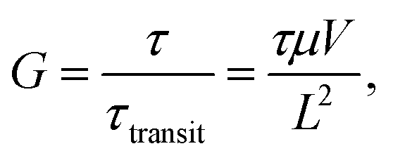
Nevertheless, PM-OPDs have one critical drawback of a slow temporal response – that is, a low −3 dB bandwidth. This is because the photoconductive gain is determined by
| |  | (1) |
where
τ is the carrier lifetime,
τtransit is the carrier transit time,
μ is the carrier mobility,
V is the applied bias, and
L is the device length.
15,16 In the case of PM-OPDs with the donor polymer acting as a photoactive matrix, the carrier corresponds to a hole (which can be translated as
G =
τhole/
τtransit,hole).
eqn (1) is valid under the assumption that the light intensity is not strong enough to fill all the trap states. Because carrier lifetime is closely related to the response time and is artificially engineered to be long enough to generate a photoconductive gain, PM-OPDs with a high EQE of more than 10
000% typically possess low bandwidth values of less than 100 Hz, thus a low gain–bandwidth product under 10
000 Hz is obtained.
6,13,15,17 This is a critical limitation of PM-OPDs because most video applications require a −3 dB bandwidth of at least several hundred hertz. Thus, the question of enhancing the response time of PM-OPDs without significantly sacrificing photoconductive gain must be addressed. Some of the relevant theoretical studies on photoconductors predict that the response time of a photoconductor is not simply the carrier lifetime, but rather a function of both the carrier lifetime and the number of trapped charge carriers.
18 Therefore, it is essential to develop photoactive donor polymers with the desired trap density as well as a high hole mobility so that a high gain–bandwidth product can be obtained.
In this work, a new donor–acceptor copolymer, poly[4,8-bis(5-(2-hexyldecyl)thiophen-2-yl)benzo[1,2-b:4,5-b′]dithiophene] [5,5′-bis(7-(4-(2-butyloctyl)thiophen-2-yl)-6-fluorobenzo[c][1,2,5]thiadiazol-4-yl)-2,2′-bithiophene] (PDBD-FBT), was designed and synthesized. Dithienyl-benzo [1,2-b′:4,5-b′] dithiophene (DT-BDT) was introduced to enhance intermolecular π–π stacking, and 5-fluoro-2,1,3-benzothiadiazole was introduced to obtain suitable highest occupied molecular orbital (HOMO) and lowest unoccupied molecular orbital (LUMO) energy levels for use as the photoactive layer of a PM-OPD. In particular, the fluorine and alkyl groups were designed to have a certain direction, that is, the regioregularity of the resulting copolymer was maximized. Owing to the extraordinary regioregularity of PDBD-FBT, the resulting films showed low paracrystalline disorder as well as a highly oriented face-on structure, which enabled a low trap density in the diode structure resulting in a high bulk mobility. Theoretical analyses of the carrier lifetime in relation to the response time are provided by solving the rate equation for the free charge carrier in order to explain the high gain–bandwidth product of more than 400000 Hz in the proposed PDBD-FBT PM-OPD.
Results and discussion
Synthesis
Scheme 1 describes the synthetic details of PDBD-FBT. The regioregularity of this polymer was acquired from a symmetric macromonomer, where thiophene and mono-fluoro-benzothiadiazole-based symmetric compound 1 was obtained by using a side product of the Stille coupling reaction, as shown in Scheme S1 (ESI†). This side product has a symmetrical structure of thiophene and benzothiadiazole with mono-substitution of alkyl and fluorine side chains, which can induce the formation of a regioregular polymer. Moreover, S⋯F non-covalent interactions between the sulfur of thiophene and fluorine of benzothiadiazole may cause extended conjugation of the π-orbital, which leads to strong π–π stacking properties and planarity.19 In addition, approximately 17% of the mono-Sn-substituted reactant was consumed to produce side products during the Stille coupling reaction; thus, the amount of monomer was sufficient to make the polymer.
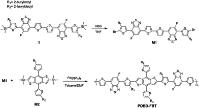 |
| | Scheme 1 The synthetic route for the monomer and polymerization route for PDBD-FBT. | |
Initially, bromination of compound 1 using NBS produced the dibromo monomer, M1 (Fig. S1, ESI†). After bromination, the regioregular PDBD-FBT was synthesized using Stille cross-coupling polymerization between M1 and the distannyl-DT-BDT monomer, M2. To ensure the solubility of the final polymer, DT-BDT with hexyldecyl side chains was used as a monomer. After polymerization, crude polymers were purified by Soxhlet extraction with methanol, acetone, hexane, dichloromethane, and chlorobenzene, and the polymers of the chlorobenzene fraction were produced as a dark black solid in 88% yield. PDBD-FBT is soluble in hot chlorinated solvents, such as chlorobenzene, o-dichlorobenzene, and chloroform. The number average molecular weight (Mn) and weight average dispersity (Đ, Mw/Mn) of PDBD-FBT were determined by carrying out gel permeation chromatography at 80 °C in chlorobenzene as an eluent. The Mn and Đ values are 11.9 K and 3.04, respectively. No phase transition was observed at 30–330 °C according to differential scanning calorimetry measurement (Fig. S2, ESI†).
Structural analyses
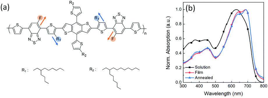
The scheme of regioregular alkyl and fluorine side chains in the PDBD-FBT molecular structure is shown in Fig. 1a. Fig. 1b shows the absorption spectra of PDBD-FBT in both dichlorobenzene solution and solid film states. In the solution state, PDBD-FBT shows typical dual-band absorption, band I (500–800 nm) and band II (300–500 nm). This dual-band can be attributed to intramolecular charge transfer between electron-donating and electron-withdrawing groups and localized π–π* transitions, respectively. In particular, distinct 0–0 and 0–1 vibronic features are observed in band I at ∼690 and 630 nm, respectively, implying polymer aggregation with short-range π–π stacking, even in dilute solution, because of the high molecular rigidity with backbone planarity.20 When the polymer state transition occurs from solution to film, the relative 0–0 absorption peak intensity increases with a decrease in the 0–1 absorption peak, resulting in the maximum absorption (λmax) of the polymer in solution and film states located at 632 and 689 nm, respectively. This is a typical feature of regioregular polymers, indicating an enhanced rearrangement of PDBD-FBT with strong π–π stacking between the polymer chain backbones in the solid film,21–23 which is subsequently enhanced in the annealed film. From such improved ordering and planarization of the polymer film, efficient intermolecular interactions and charge carrier transport can be expected in the device.
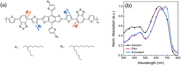 |
| | Fig. 1 (a) Molecular structure of regioregular PDBD-FBT. (b) UV-Vis absorption spectra of PDBD-FBT in solution and thin film states. | |
Two-dimensional grazing incidence X-ray diffraction (2D-GIXD) analysis was conducted, using the PLS-II 3C and 9A beamline at the Pohang Accelerator Laboratory (PAL) in Korea, to investigate the crystalline ordering and orientation of the PDBD-FBT neat films and its blend films with ITIC (100:1, w/w), which corresponds to the PM-OPD device fabrication condition. The obtained diffraction images and line-cut profiles are shown in Fig. 2a–f. The 2D-GIXD patterns of the neat polymer and blend films with thermal annealing at 150 °C for 10 min showed improved lamellar ordering with side alkyl chain stacking (h00) as well as π–π stacking (010) in the neat and blend films. In addition, the diffraction patterns of the blend films are almost the same as those of the neat films, implying that the addition of 1 wt% ITIC does not significantly alter the crystalline ordering and orientation of PDBD-FBT. For example, (100) diffractions were observed at qz = 0.302 and 0.311 Å−1 for the neat and blend films, respectively, in the pristine case, and at qz = 0.298 and 0.300 Å−1 for the neat and blend films, respectively, in the annealed case. Because π–π stacking features (qz = 1.744 or qxy = 1.753 Å−1) and lamellar ordering features (h00) are observed both in the out-of-plane and in-plane directions, it can be argued that a bimodal orientation is adopted in the PDBD-FBT neat film and blend film with ITIC. Based on the peak positions of (100) and (010), the d-spacing and π–π stacking distance values of the films were estimated, as summarized in Table 1. For PM-OPDs, where the charge carrier mobility occurs vertical direction to the substrates, the face-on orientation is more favorable.22 For quantitative comparison of the crystalline orientation, pole figure analysis was performed for the (010) diffraction, as shown in Fig. 2g. The PDBD-FBT neat film shows bimodal distributions in the π-systems with a face-on portion of 96.4% and edge-on portion of 3.6%, and the face-on portion is slightly increased to 97.3% in the blend film. This high portion of π–π stacking along the out-of-plane direction indicates a highly oriented face-on structure. Together with the short π–π stacking distances, one can speculate that there is a large π–π overlap between adjacent molecular units in the face-on orientation, which contributes to the advantageous charge transport and reduces the number of trapping sites.
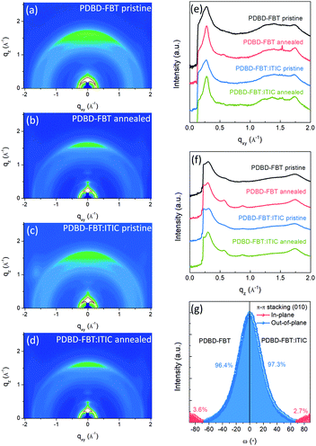 |
| | Fig. 2 (a–d) 2D-GIXD pattern images for PDBD-FBT neat films and PDBD-FBT:ITIC (100:1, w/w) blend films. (e and f) Corresponding line-cut profiles of in-plane and out-of-plane directions, respectively. (g) Pole figure analysis for π–π stacking of annealed films. | |
Table 1 Summary of 2D-GIXD parameters of the neat polymer and blend films
|
|
d-Spacing (Å) |
π–π Stacking distance (Å) |
g
(010) (%) |
g
(h00) (%) |
| Pristine PDBD-FBT |
21.14 |
3.65 |
23.57 |
— |
| Annealed PDBD-FBT |
21.33 |
3.61 |
9.62 |
3.03 |
| Pristine PDBD-FBT:ITIC |
20.53 |
3.64 |
12.67 |
— |
| Annealed PDBD-FBT:ITIC |
20.95 |
3.62 |
10.46 |
3.95 |
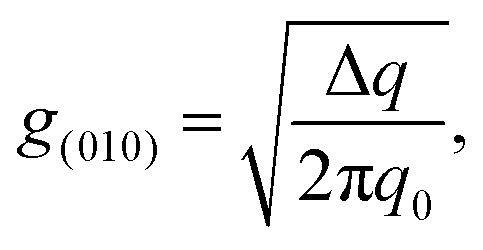
From 2D-GIXD data, it is possible to calculate the paracrystalline disorder (g), which is related to the structural disorder in an imperfect crystal and thus the electrical trap states of the polymer film.24,25 The paracrystalline disorder parameter for the (010) peaks (g(010)) can be calculated by using the single peak-width estimation method based on
| |  | (2) |
where Δ
q is the width of the diffraction peak and
q0 is the center position of the peak. The paracrystalline disorder can also be analyzed for the (
h00) peaks by calculating the slope (
m) of a
δb –
h2 plot (Fig. S3, ESI
†), which is determined by
| |  | (3) |
where
d is the domain spacing,
δb is the integral width of the diffraction peaks, and
h is the order of diffraction. The calculated paracrystalline disorder parameters,
g(010) and
g(h00), of the annealed films were 9.62% and 3.03% for the neat film and 10.46% and 3.95% for the blend film, respectively. Considering that the paracrystalline disorder values of most donor–acceptor copolymers range from 10% to 15%,
26,27 the obtained
g(010) and
g(h00) values of PDBD-FBT imply that the polymer is relatively well ordered in both the out-of-plane and in-plane directions with low structural disorder, which can be ascribed to the regioregularity of the polymer, as demonstrated by UV-Vis spectroscopy. Collectively, the annealed blend film, which corresponds to the PM-OPD device condition, shows a preferential face-on orientation and low paracrystalline disorder, which can lead to high charge carrier mobility in the PM-OPD device.
PM-OPDs
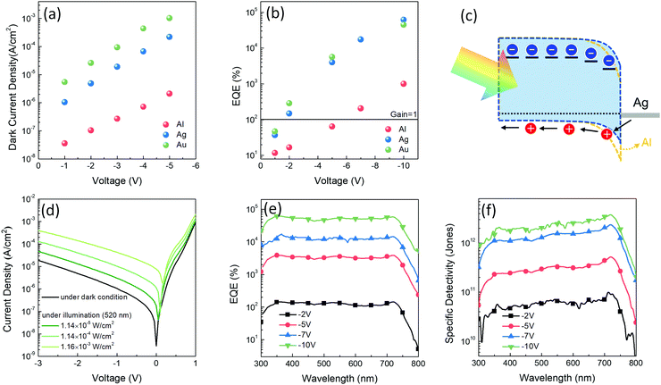
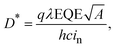
In this study, three device architectures were prepared for PM-OPDs with a difference only in the cathodes – that is, ITO/PEDOT:PSS/PDBD-FBT:ITIC/cathode, where the cathode varies as Al, Ag, and Au. In PM-OPDs, because the photogenerated and subsequently trapped electrons are responsible for the injection of holes through the thinned Schottky barrier, varying the cathode metal can change the gain generation efficiency. Because the Schottky barrier height is defined as the difference between the ionization energy of the semiconductor and the work function of the metal, in the given device architecture, the HOMO level of PDBD-FBT and the work function of the cathode determine the Schottky barrier height. According to cyclic voltammetry (Fig. S4, ESI†), PDBD-FBT has a HOMO level of −5.14 eV, which is apparently deeper than that of poly(3-hexylthiophene) (P3HT), which is commonly used as an active matrix of PM-OPD.28–31 This implies that the commonly used Al cathode (work function = 4.3 eV) may not be a good choice in this case because of its too high Schottky barrier height. Therefore, the changes in the dark current density and EQE values of the PDBD-FBT devices were evaluated according to the choice of cathode. Fig. 3a and b show the dark current density and EQE values of the devices, respectively, under reverse biases depending on the choice of cathode. As the work function increases for Al, Ag, and Au (4.3, 4.7, and 5.1 eV, respectively), the Schottky barrier height can be lowered, resulting in a high dark current. However, a low Schottky barrier height is advantageous for hole injection; thus, a gain mechanism and high EQE can be generated at low voltages. As highlighted in Fig. 3b, both Ag and Au enable a high EQE at low voltages, while Al enables an EQE of more than 100% only with an exceptionally high voltage of −7 V, which is clearly different from previous PM-OPD studies in which P3HT with a relatively low ionization potential was used. Although Au, which facilitates a near-Ohmic junction with PDBD-FBT, is more advantageous for gain generation at low voltage, it has a substantially high dark current, as shown in Fig. 3a, which is detrimental to achieving a high signal-to-noise ratio. Therefore, Ag was chosen as a cathode that can simultaneously facilitate both a low dark current and a high EQE. The detailed J–V characteristics, EQE, and specific detectivity spectra of the Al and Au devices are summarized in Fig. S5 and S6 (ESI†), respectively. The scheme of photocurrent generation for the optimized device of a PDBD-FBT PM-OPD is shown in Fig. 3c. When the photogenerated electrons are trapped in ITIC, extra holes are injected more easily by the lowered Schottky barrier, resulting in a high photoconductive gain, even under a low bias. The J–V characteristics with various light intensities are summarized in Fig. 3d. EQE spectra under different reverse biases are shown in Fig. 3e with a peak value of 62100% at 355 nm under −10 V. In particular, the photoconductive gain begins to occur under a low bias of −2 V, which can be explained by the optimized Schottky barrier height.
 |
| | Fig. 3 (a and b) Dark current density and EQE values of PDBD-FBT devices with the ITO/PEDOT:PSS/PDBD-FBT:ITIC/cathode (Al, Ag, or Au) structure under various reverse biases, respectively. (c) Schematic description of photocurrent generation of the optimized PM-OPD. The lowered Schottky barrier can facilitate injection of holes. (d) J–V characteristics of the optimized PM-OPD under dark and illuminated (520 nm wavelength) conditions. (e and f) EQE and specific detectivity spectra under various reverse biases with a light intensity of 11.4 μW cm−2 (at 520 nm), respectively. | |
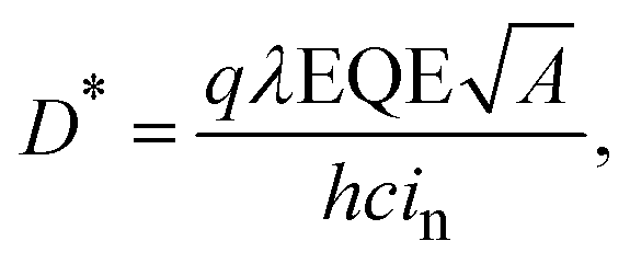
The specific detectivity (D*), which is an important figure-of-merit of PM-OPDs, is defined as
| |  | (4) |
where
λ is the illumination wavelength,
A is the area of the active layer,
h is Planck's constant,
c is the speed of light, and
in is the noise current.
14 The noise current and calculated specific detectivity spectra are summarized in Fig. S7 (ESI
†) and
Fig. 3f, respectively, showing that the peak detectivity under −10 V is 3.82 × 10
12 Jones at 720 nm. Because the gain generation mechanism is a strong function of light intensity in PM-OPDs, it is important to check the linear dynamic range (LDR). The LDR was measured under 520 nm light illumination with different light intensities from 1.16 × 10
−8 W cm
−2 up to 1.8 × 10
−2 W cm
−2. Assuming that the noise equivalent power of the fabricated PM-OPD can be regarded as the lowest limit of the LDR, high LDR values of 122, 117, 116, and 115 dB were obtained under reverse biases of 2, 5, 7, and 10 V, respectively (Fig. S8, ESI
†).
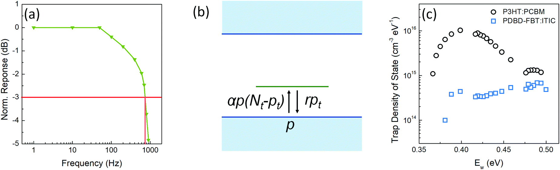
Lifetime and response time
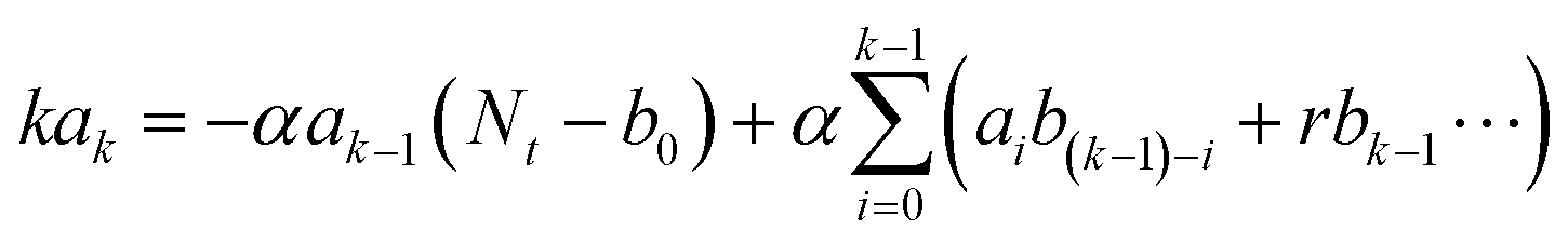
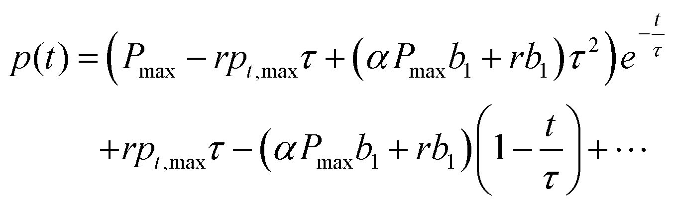
As explained in the introduction section, despite the high EQE, the slow response time of PM-OPDs can limit their practical application in image sensors. However, interestingly, the PDBD-FBT PM-OPD in this study exhibited a rather high −3 dB bandwidth of ∼740 Hz, as summarized in Fig. 4a. As shown in Table 2, such a high bandwidth has not been reported in previous studies on PM-OPDs with a reasonably high EQE >10000%.6,15,17,32 Note that the gain–bandwidth product values gathered in Table 2 were chosen with strict regulation in terms of the constant light intensity for measurements of both gain and bandwidth. This is because a weak light intensity is advantageous for the gain and a strong light intensity is advantageous for the bandwidth.33 It is known that the response time (τ0) of an OPD is determined by τ0 = 0.35/f−3dB; thus, the calculated τ0 from Fig. 4a is 473 μs. If τ0 is directly translated to the carrier lifetime, τ, then according to eqn (1), gain values can be estimated to be ∼2130 considering the bulk hole mobility of PDBD-FBT of ∼1.8 × 10⁻⁴ cm2 V−1 s−1, which was extracted from space-charge-limited current analysis, as summarized in Fig. S9 (ESI†). The estimated gain value with the assumption of τ~τ0 is much higher than the actual gain of ∼600, implying that τ0 is essentially higher than τ. Therefore, to completely understand the origin of the simultaneously obtained high gain and bandwidth – that is, a high gain–bandwidth product exceeding 400000 Hz of the PDBD-FBT based PM-OPD – it is essential to quantitatively correlate the carrier lifetime with response time. A simple model assuming a single set of trapping levels for the hole was introduced, as shown in Fig. 4b. With this model, one can write the rate equation for the free hole density as| | 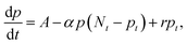 | (5) |
where A is the photogeneration rate of electron–hole pairs per unit time, α is the capture cross-section for a particular type of traps at a given temperature, p is the free hole density, Nt is the total number of traps, pt is the number of occupied traps, and r is the probability of rejection of holes to the valence band by thermal agitation.34 This equation can be solved by a series of solutions for the photocurrent decay condition.| |  | (6) |
| |  | (7) |
 |
| | Fig. 4 (a) Bode plot under green (520 nm) light illumination with an intensity of 11.4 μW cm−2 measured at −10 V. (b) Single set model of trapping levels for hole. (c) Trap state densities of PDBD-FBT:ITIC (100:1, w/w) film and P3HT:PCBM (100:1, w/w) reference film obtained using the thermal admittance spectroscopy method. | |
Table 2 Gain–bandwidth products of previously reported PM-OPDs where gain and bandwidth measurements were performed at the same light intensity
| Ref. |
Applied bias (V) |
Light intensity (μW cm−2) |
Gain |
Response time (ms) |
Bandwidth (Hz) |
Gain–bandwidth product (Hz) |
|
Rise time.
Fall time.
Bandwidth calculated by f−3dB = 0.35/response time.
Measured −3 dB frequency.
|
|
32
|
−5 |
8200 |
20 |
300ab |
1.17c |
23.3 |
|
17
|
−1 |
45 |
20 |
200a, 180b |
1.75c |
35 |
|
6
|
−10 |
8.87 |
200 |
1500a |
0.23c |
46 |
|
15
|
−0.5 |
7.5 |
200 |
270b |
6.7d |
1340 |
|
This work
|
−10
|
11.4
|
600
|
0.5
, 3
|
740
|
444![[thin space (1/6-em)]](https://www.rsc.org/images/entities/b_char_2009.gif) 000 000
|
When applying eqn (6) and (7) to eqn (5), the coefficients a1,a2,… can be obtained by
| |  | (8) |
After reaching a steady state of photocurrent, the radiation is turned off,
A becomes 0 and
a0 =
Pmax,
b0 =
pt,max can be assumed. Then, one can substitute the coefficients from
eqn (8) for those of
eqn (6). Finally, the equation can be solved in its exponential form as
| |  | (9) |
Thereafter, by fitting the transient photocurrent in Fig. S10 (ESI
†) with
eqn (9), the carrier lifetime can be extracted. The obtained
τ of 134 μs is lower than
τ0 and matches well with the observed gain value owing to the gain of ∼600 predicted from
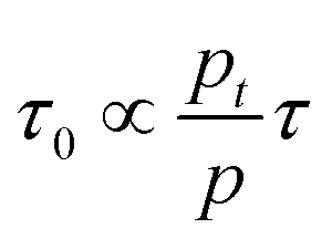
eqn (1), which is in good agreement with the actual measurement. One previous study on photoconductivity predicted that
| |  | (10) |
which implies that both the carrier lifetime and number of trapped charges determine the resulting response time of a PM-OPD. As demonstrated in
Fig. 2, PDBD-FBT has a relatively low paracrystalline disorder with a highly oriented face-on structure owing to its regioregularity, which leads to a low trap density. To analyze the actual electrical trap distribution in the PDBD-FBT PM-OPD, the thermal admittance spectroscopy (TAS) method was employed.
Fig. 4c shows that the PDBD-FBT
:
ITIC (100
:
1 w/w) has a relatively low trap state density of approximately 10
14–10
15 cm
−3 eV
−1 in the entire spectral range. For comparison, an ITO/PEDOT:PSS/P3HT:PCBM/Al reference device was also fabricated. Although the gain value of this reference device is similar to that in the present study, the −3 dB frequency was far lower (∼50 Hz) (Fig. S11, ESI
†). A Mott–Schottky plot to extract built-in potential values of the two devices, which is required to calculate the trap state density, is shown in Fig. S12 (ESI
†). Interestingly, TAS analysis on this reference device evidently showed a higher trap density of 10
15–10
16 cm
−3 eV
−1, which implies that regioregular PDBD-FBT with three-dimensional ordering allows few defect states to form along the vertical charge transport direction, expediting the response speed when applied as the active matrix of a PM-OPD.
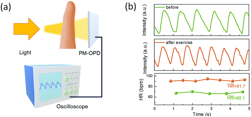
Application in photoplethysmography
To verify the feasibility of the PM-OPD with a sufficiently fast response speed, a practical application of photoplethysmography (PPG) analysis was conducted.35 In PPG measurements, a PM-OPD receives the reflected or transmitted light from a finger, and volume changes in the blood vessels cause fluctuations in the reflected/transmitted light intensity, as depicted in Fig. 5a. The PM-OPD signal resulting from the contraction and expansion of the vessels can detect the heartbeat. The PPG measurements were conducted before and after strenuous exercise with the PM-OPD, and heart rates were calculated to be 68.1 and 91.7 bpm, respectively (Fig. 5b).
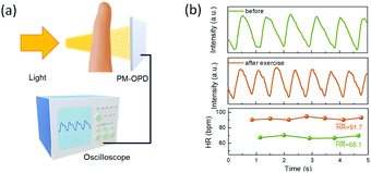 |
| | Fig. 5 (a) Setup of PPG measurement with the PM-OPD based on PDBD-FBT. (b) Measured PPG spectra before and after strenuous exercise. | |
Discussion
Eqn (1) predicts that the photoconductive gain of a p-type PM-OPD is determined by the multiple recirculation of free holes before recombination with captured electrons. Apparently, a longer hole lifetime and shorter transit time should be a key solution for achieving a high gain in PM-OPDs. Although a high hole mobility is anticipated to be essential for a PM-OPD to shorten the hole transit time, one should consider a tradeoff relation between response time and gain considering the hole lifetime. It is evident that a long carrier lifetime can result in a slow transient response. After light is turned off, a long carrier lifetime can lead to persistent photoconductivity because of the gain generation mechanism. However, such a long carrier lifetime is directly related to the photoconductive gain according to eqn (1). Considering that the recombination-limited hole lifetime is determined by the energetics and density of recombination centers, PM-OPDs with a small portion of acceptor molecules should have similar hole lifetimes if the donor and acceptor molecules are molecularly well mixed and the LUMO level offsets are sufficiently high. This is why most PM-OPD studies have yielded similar gain values of 100–1000 (EQE 10000–100000%). Subsequently, maximizing the bandwidth of the PM-OPD with a given carrier lifetime can be achieved by decreasing the trap densities (of multiple trapping and release models) according to eqn (10). In other words, the direct tradeoff relation is valid only for carrier lifetime and gain and is not valid for response time and gain. If relevant trap engineering is used, a simultaneous enhancement of the response time and gain is possible to a certain extent. This study shows that molecular engineering can provide low electrical trap densities for vertical charge transport in PM-OPDs so that a high bandwidth of more than 700 Hz can be obtained without severely sacrificing the high gain, resulting in an unprecedentedly high gain–bandwidth product exceeding 400000 Hz.
Conclusions
A molecular approach was presented to overcome the slow temporal response of PM-OPDs such that a high gain–bandwidth product exceeding 400000 Hz could be achieved. A new donor–acceptor copolymer, PDBD-FBT, strategically designed to have a highly regioregular conformation was synthesized by means of Stille coupling and applied as the active layer of a PM-OPD by blending with a small amount of ITIC. Owing to the intrinsically introduced regioregularity of the polymer, a highly oriented face-on crystalline structure with relatively low paracrystalline disorder was obtained, as confirmed by 2D-GIXD analyses. As a result, the PDBD-FBT PM-OPD device exhibited a low electrical trap density of 1014–1015 cm−3 eV−1 according to the TAS study. Based on the analytical solution of the rate equation assuming a single set of trapping levels, it was shown that such a low trap density could induce a short response time resulting in a high bandwidth despite a long carrier lifetime, implying that the response time and gain were not in a direct tradeoff relation. Therefore, a high EQE of more than 60000% was achieved while maintaining a fast response time with a –3 dB cutoff frequency of ∼740 Hz, leading to a gain–bandwidth product of more than 4 × 10⁵ Hz and a high specific detectivity of 3.82 × 10¹² Jones.
Conflicts of interest
There are no conflicts to declare.
Acknowledgements
This research was supported by a Basic Science Research Program through the National Research Foundation of Korea (NRF) funded by the Ministry of Science, ICT & Future Planning (Grant Number NRF-2018R1A2B6003445). This research was also supported by a KRICT project (KS2041-20) from the Korea Research Institute of Chemical Technology.
References
- G. Maiellar, E. Ragonese, R. Gwoziecki, S. Jacobs, M. Marjanović, M. Chrapa, J. Schleuniger and G. Palmisano, IEEE Trans. Circuits Syst. I, Reg. Papers, 2014, 61, 1036 Search PubMed.
- N. Strobel, M. Seiberlich, R. Eckstein, U. Lemmer and G. Hernandez-Sosa, Flexible Printed Electron., 2019, 4, 043001 CrossRef CAS.
- C. M. Lochner, Y. Khan, A. Pierre and A. C. Arias, Nat. Commun., 2014, 5, 5745 CrossRef CAS.
- T. Yokota, P. Zalar, M. Kaltenbrunner, H. Jinno, N. Matsuhisa, H. Kitanosako, Y. Tachibana, W. Yukita, M. Koizumi and T. Someya, Sci. Adv., 2016, 2, e1501856 CrossRef.
- H.-Y. Chen, M. K. F. Lo, G. Yang, H. G. Monbouquette and Y. Yang, Nat. Nanotechnol., 2008, 3, 543 CrossRef CAS.
- W. Wang, F. Zhang, L. Li, M. Zhang, Q. An, J. Wang and Q. Sun, J. Mater. Chem. C, 2015, 3, 7386 RSC.
- M. S. Jang, S. Yoon, K. M. Sim, J. Cho and D. S. Chung, J. Phys. Chem. Lett., 2018, 9, 8 CrossRef CAS.
- M. R. Esopi, M. Calcogno and Q. Yu, Adv. Mater. Technol., 2017, 2, 1700025 CrossRef.
- L. Li, F. Zhang, W. Wang, Y. Fang and J. Huang, Phys. Chem. Chem. Phys., 2015, 17, 30712 RSC.
- Z. Zhao, J. Wang, C. Xu, K. Yang, F. Zhao, K. Wang, X. Zhang and F. Zhang, J. Phys. Chem. Lett., 2020, 11, 366 CrossRef CAS.
- W. T. Hammond, J. P. Mudrick and J. Xue, J. Appl. Phys., 2014, 116, 214501 CrossRef.
- Z. Zhao, C. Li, L. Shen, X. Zhang and F. Zhang, Nanoscale, 2020, 12, 1091 RSC.
- W. Wang, F. Zhang, M. Du, L. Li, M. Zhang, K. Wang, Y. Wang, B. Hu, Y. Fang and J. Huang, Nano Lett., 2017, 17, 1995 CrossRef CAS.
- D. K. Neethipathi, H. S. Ryu, M. S. Jang, S. Yoon, K. M. Sim, H. Y. Woo and D. S. Chung, ACS Appl. Mater. Interfaces, 2019, 11, 21211 CrossRef CAS.
- X. Zhou, D. Yang, D. Ma, A. Vadim, T. Ahamad and S. M. Alshehri, Adv. Funct. Mater., 2016, 26, 6619 CrossRef CAS.
- M. Daanoune, R. Clerc, B. Flament and L. Hirsch, J. Appl. Phys., 2020, 127, 055502 CrossRef CAS.
- D. Y. Kim, J. Ryu, M. Manders, J. Lee and F. So, ACS Appl. Mater. Interfaces, 2016, 6, 1370 CrossRef.
-
L. Biberman, Photoelectronic Imaging Devices: Physical Processes and Methods of Anaysis, Springer, US, 1971 Search PubMed.
- Y.-S. Lee, J. Y. Lee, S.-M. Bang, B. Lim, J. Lee and S.-I. Na, J. Mater. Chem. A, 2016, 4, 11439 RSC.
- K. H. Park, K. H. Cheon, Y.-J. Lee, D. S. Chung, S.-K. Kwon and Y.-H. Kim, Chem. Commun., 2015, 51, 8120 RSC.
- S. W. Kim, H. Kim, J.-W. Lee, C. Lee, B. Lim, J. Lee, Y. Lee and B. J. Kim, Macromolecules, 2019, 52, 738 CrossRef CAS.
- K. Kanai, T. Miyazaki, H. Suzuki, M. Inaba, Y. Ouchi and K. Seki, Phys. Chem. Chem. Phys., 2010, 12, 273 RSC.
- B. Lim, D. X. Long, S.-Y. Han, Y.-C. Nah and Y.-Y. Noh, J. Mater. Chem. C, 2018, 6, 5662 RSC.
- R. Noriega, J. Rivnay, K. Vandewal, F. P. V. Koch, N. Stingelin, P. Smith, M. F. Toney and A. Salleo, Nat. Mater., 2013, 12, 1038 CrossRef CAS.
- J. Rivnay, R. Noriega, J. E. Northrup, R. J. Kline, M. F. Toney and A. Selleo, Phys. Rev. B: Condens. Matter Mater. Phys., 2011, 84, 045203 CrossRef.
- H. Ko, S. Park, H. J. Son and D. S. Chung, Chem. Mater., 2020, 32, 3219 CrossRef CAS.
- A. Giovannitti, I. P. Maria, D. Hanifi, M. J. Donahue, D. Bryant, K. J. Barth, B. E. Makdah, A. Savva, D. Moia, M. Zetek, P. R. F. Barnes, O. G. Reid, S. Inal, G. Rumbles, G. G. Malliaras, J. Nelson, J. Rivnay and I. McCulloch, Chem. Mater., 2018, 30, 2945 CrossRef CAS.
- L.-L. Chua, J. Zaumseil, J.-F. Chang, E. C.-W. Ou, P. K.-H. Ho, H. Sirringhaus and R. H. Friend, Nature, 2005, 434, 194 CrossRef CAS.
- X.-L. Hu, L.-J. Zuo, Y.-X. Nan, M. Helgesen, O. Hagemann, E. Bundgaard, M.-M. Shi, F. C. Krebs and H.-Z. Chen, Synth. Met., 2012, 23, 162 Search PubMed.
- J. B. Kim, K. Allen, S. J. Oh, S. Lee, M. F. Toney, Y. S. Kim, C. R. Kagan, C. Nuckolls and Y.-L. Loo, Chem. Mater., 2010, 22, 5762 CrossRef CAS.
- C.-C. Ho, Y.-C. Liu, S.-H. Lim and W.-F. Su, Macromolecules, 2012, 45, 813 CrossRef CAS.
- K. Yang, J. Wang, J. Miao, J. Zhang and F. Zhang, J. Mater. Chem. C, 2019, 7, 9633 RSC.
- J. P. Clifford, G. Konstantatos, K. W. Johnston, S. Hoogland, L. Levina and E. H. Sargent, Nat. Nanotechnol., 2009, 4, 40 CrossRef CAS.
- N. V. Joshi, Phys. Rev. B: Condens. Matter Mater. Phys., 1983, 27, 6272 CrossRef CAS.
- M. Kang, S.-M. Ko, J. Kim, S. Z. Hassan, D.-W. Jee and D. S. Chung, Mater. Horiz., 2020, 7, 3034 RSC.
Footnote |
| † Electronic supplementary information (ESI) available. See DOI: 10.1039/d0mh01588a |
|
| This journal is © The Royal Society of Chemistry 2021 |
Click here to see how this site uses Cookies. View our privacy policy here. 
 *c and
Dae Sung
Chung
*c and
Dae Sung
Chung