
 Open Access Article
 This Open Access Article is licensed under a Creative Commons Attribution-Non Commercial 3.0 Unported Licence
Patterning and control of the nanostructure in plasma thin films with acoustic waves: mechanical vs. electrical polarization effects†
Aurelio
García-Valenzuela
a,
Armaghan
Fakhfouri
b,
Manuel
Oliva-Ramírez
a,
Victor
Rico-Gavira
a,
Teresa Cristina
Rojas
a,
Rafael
Alvarez
a,
Siegfried B.
Menzel
b,
Alberto
Palmero
a,
Andreas
Winkler
 *b and
Agustín R.
González-Elipe
*a
*b and
Agustín R.
González-Elipe
*a
aNanotechnology on Surfaces and Plasma Laboratory, Instituto de Ciencia de Materiales de Sevilla (CSIC-Univ. Sevilla), Avda. Américo Vespucio 49, 41092 Sevilla, Spain. E-mail: arge@icmse.csic.es
bIFW Dresden, SAWLab Saxony, Helmholtzstr. 20, 01069 Dresden, Germany. E-mail: a.winkler@ifw-dresden.de
First published on 9th December 2020
Abstract
Nanostructuration and 2D patterning of thin films are common strategies to fabricate biomimetic surfaces and components for microfluidic, microelectronic or photonic applications. This work presents the fundamentals of a surface nanotechnology procedure for laterally tailoring the nanostructure and crystalline structure of thin films that are plasma deposited onto acoustically excited piezoelectric substrates. Using magnetron sputtering as plasma technique and TiO2 as case example, it is demonstrated that the deposited films depict a sub-millimetre 2D pattern that, characterized by large lateral differences in nanostructure, density (up to 50%), thickness, and physical properties between porous and dense zones, reproduces the wave features distribution of the generated acoustic waves (AW). Simulation modelling of the AW propagation and deposition experiments carried out without plasma and under alternative experimental conditions reveal that patterning is not driven by the collision of ad-species with mechanically excited lattice atoms of the substrate, but emerges from their interaction with plasma sheath ions locally accelerated by the AW-induced electrical polarization field developed at the substrate surface and growing film. The possibilities of the AW activation as a general approach for the tailored control of nanostructure, pattern size, and properties of thin films are demonstrated through the systematic variation of deposition conditions and the adjustment of AW operating parameters.
New conceptsMain breakthrough of this work is the demonstration that assisting the plasma deposition of thin films with acoustic waves (AWs) leads to patterning phenomena characterized by substantial lateral changes in nanostructure, thickness and properties. In addition, changes in crystal structure are also induced. The implications of these patterning phenomena to laterally tailor the properties of thin films are huge and open a new methodology for the of manufacturing of materials. The reported experiment entails the merging of two physical processes that have never been considered together: plasma interaction during atom deposition and acoustic wave activation. Ultrasounds, generally in the kHz range and propagating in fluid media are a common tool to induce cleaning, phase separations or even chemical reactions. However, AWs in the MHz range and propagating through piezoelectric materials, although pervasive in different technological domains (sensors, actuators and other operating devices), have never been used to assist the deposition of a thin film in a vacuum and/or plasma environment. We envisage that the implications in material science of this combination of phenomena and, likely, other type of excitation processes yet unexplored, will provide new tools for the pattering of thin films during growth, as well as for their surface activation. |
Introduction
Thin film deposition by evaporation, sputtering or plasma-based techniques over large areas, are crucial processes for various applications in research laboratories as well as in industry. While mature technologies are readily available for deposition, efficient control over the nanostructure of the deposited layers still remains a challenge.1 To this end, thin film plasma deposition has been assisted by a large variety of methods including thermal activation,2 ion bombardment,3,4 or the application of magnetic fields.5 Similarly, nano-, micro- or macro-patterning of this type of thin films is at the core of modern key technologies, and thus this has prompted the development of a large variety of ad hoc post-deposition techniques. Examples include, but are not limited to, various types of lithography, several wet routes and laser patterning methods.6–8 However, very little attention has been devoted to the control of plasma thin films nanostructures and their patterning via the periodicity and energy activation capabilities of acoustic waves (AWs) propagating through an active substrate.9Standing AWs are generated upon application of AC electrical signals that produce localized, time dependent mechanical deformations and associated electrical polarizations that take place due to the so-called inverse and direct piezoelectric effects, respectively.9 In the simplest case, a sinusoidal AC signal in the MHz range is applied to planar electrodes to generate Lamb-type plate waves with amplitudes of few tens of nanometers.10 Alternatively, a set of interdigitated transducers (IDT)11 is employed to generate Rayleigh-type surface acoustic waves (SAW). SAW are widely used for key technological applications in the fields of sensors, transducers and microfluidic actuators.12–14 Beyond these classical applications, AWs are demonstrating emerging possibilities for activation and modification of different material responses. Examples include the modulation of the optical and electrical properties of graphene,15,16 the magnetization of ferromagnetic thin films,17 the generation of a photoflexoelectric effect in halide perovskites solar cells,18 and the induction of lens focusing effects for the rheological analysis of tiny volumes of liquids.19 Surface propagating SAWs have been also used for the processing of nanomaterials in liquid media through the deposition of organic thin films20 or the patterned deposition of nanowires,21 nanoparticles22 or carbon nanotubes.23 In spite of the widespread use of AWs, the interactions between AWs and low pressure plasmas with the objective of assisting the growth of thin films is an unexplored subject as evidenced in a recent road map analysis on the subject.24
Plasmas at the nanoscale are rather complex systems typically characterized by multiple interactions involving free ions, electrons and other excited species.25 These interactions are modified when plasmas enter in contact with a solid surface and form a so called plasma-sheath.26 Plasma sheaths are always present when a thin film is deposited via any plasma driven procedure.25 Despite the growing emergence of AWs-plasma interactions studies with promising technological implications,27,28 the involvement of these interactions in the deposition and nano-structuration of thin films has been largely overlooked by the scientific community (to our knowledge, except for an early work by Takahashi et al.29 that will be briefly discussed later, no other attempts have addressed this problem). In the present work we report that the use of Lamb AWs significantly influence the 2D patterning of nanostructure, crystal structure and physical properties of plasma thin films. Moreover, we demonstrate that the possible interactions driven by either the direct and/or inverse piezolectrtic effects,9 are the main responsible for these structural and local nanostructural transformations. As case example to study these thin film nanostructuration and patterning processes, we choose TiO2, a widely used material,30,31 which is well characterized in terms of structure, microstructure, roughness, and other physical properties.32 We show that assisting the magnetron sputtering (MS) deposition of TiO2 with AWs generates a 2D submillimeter size pattern that mimics the AW polarization field distribution onto the surface. Most deposition experiments are carried out in an oblique angle deposition (OAD) geometry33,34 known to give rise to nanocolumnar and porous thin films. This deposition configuration is prompt to magnify any change in density associated to a 2D densification pattern. Through the simulation of AW propagating modes and the electrical field distribution developed at the substrate, our study unveils the plasma sheath–AW interaction mechanism responsible for the found patterning and nanostructuration processes. A direct evidence of this analysis is that nanostructure, pattern geometry and domain size can be tailored through the adjustment of AW characteristics. Although in this work we use Lamb-type plate AWs and a piezoelectric crystal as substrate,10 physics is transferable to other wave modes (e.g. SAWs) and propagating media (e.g., AlN or ZnO polycrystalline films deposited on any kind of substrate, including polymers35). This will open the way of using AWs as a general tool for the direct patterning of the nanostructure of a large variety of plasma thin film materials and systems.
Results and discussion
As described in the section dedicated to experimental procedures, TiO2 thin films were deposited onto a LiNbO3 substrate with electrodes on its backside. Samples are designated in the text as TiO2(νAW)-t (TiO2-t without AW excitation), where νAW and t refer, respectively, to the approximate AC frequency in MHz used for excitation and to the film equivalent thickness determined onto a simultaneously processed silicon wafer. For comparison, thin films were also deposited in a normal configuration, i.e., samples N-TiO2(νAW)-t and N-TiO2-t or by e-beam OAD evaporation, i.e., samples e-TiO2(νAW)-t and e-TiO2-t, the latter without AW excitation. The distance between the AW excited substrates and the sputtering target was kept sufficiently close to ensure that the growing film was immersed in the sputtering plasma.Nanostructure patterns in AW-assisted plasma thin films
The photograph of sample TiO2(3.4)-180 in Fig. 1A shows a patterned glare where zones of approximately 0.5 mm size can be neatly distinguished. Meanwhile, its confocal optical topography and scanning electron microscopy (SEM) analysis in Fig. 1B–D reveal that these domains present different surface heights and that, from one domain to the next, there is a progressive evolution from an irregular porous and nanocolumnar nanostructure typical of OAD thin films33,34 (for comparison, see TiO2-180 micrograph in the ESI† (S), Fig. S1), to a flat surface typical of compact ones. In other words, this patterned growth is congruent with the occurrence of a localized thin film densification process during deposition. Local changes in nanostructure give rise to different optical properties as evidenced by the reflectance spectra in Fig. 1E. From these spectra approximate refractive indexes of 1.85 and 2.2 were determined for the porous and compact domains, respectively. These values are similar to those determined over large areas for samples TiO2-200 and N-TiO2-390 deposited in OAD and normal configurations, respectively (see Fig. S2, ESI†).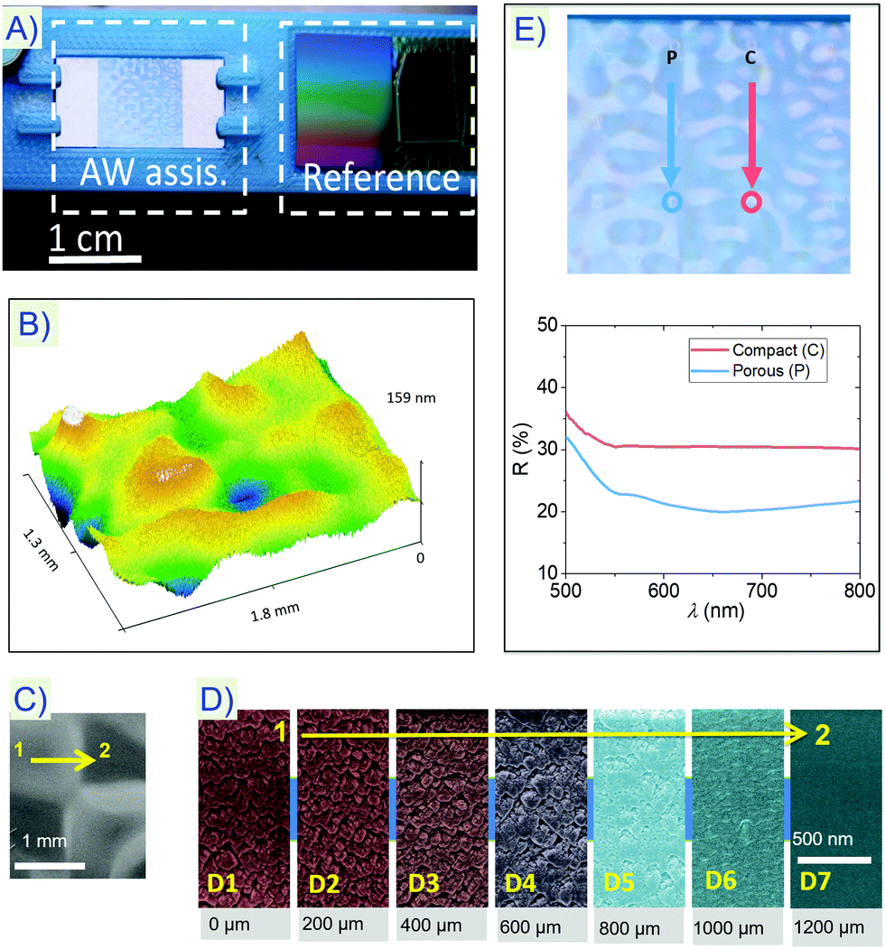 | ||
| Fig. 1 (A) Photograph of sample TiO2(3.4)-180 prepared by MS deposition in an OAD configuration under the assistance of AWs (left). To take this image, sample has been oriented to enhance the glare contrast between domains. The photograph also shows the view of sample TiO2-180 prepared simultaneously onto quartz and silicon substrates (right). (B) Confocal topography image of sample TiO2(3.4)-180. (C) Low magnification SEM micrograph taken to highlight adjacent domains with a different densification. (D) Series of top-view SEM micrographs (D1–D7) taken at ca. 200 μm intervals along a transition line connecting two adjacent domains. The numbers below the images denote the approximate step distance from position 1 to position 2 in panel (C). This series of micrographs clearly show a progressive evolution from a porous/nanocolumnar to a compact and homogeneous nanostructure. (E) Characteristic reflectance spectra taken for sample TiO2(3.4)-180 at domains with porous or compact nanostructures, i.e., equivalent to points P and C in the optical micrograph included atop from the plot. Beam size used for recording the spectra was 200 μm. | ||
Crystallographic structure of AW-assisted MS deposited TiO2
Transmission electron microscopy (TEM) analysis and electron diffraction analysis provided additional insights onto the effects of AWs on the nanostructure of plasma deposited thin films. The cross section images in Fig. 2, taken for lamellas of sample TiO2(3.4)-180 retrieved from zones D1 and D7, confirm the SEM observation in Fig. 1D of a nanocolumnar and a compact nanostructure for these zones. Remarkably, they also show an average film thickness that is approximately 200% higher at the nanocolumnar, i.e. between 190 and 150 nm, than at the compact zone, ca. 70 nm. Moreover, the High-Resolution Electron Microscopy (HRTEM) images and their corresponding Digital Diffraction Patterns (DDP's) in Fig. 2B prove the crystallization of the film. This result differs from the amorphisation found for unheated MS deposited TiO2 thin films, but agrees with the formation of anatase, rutile or a mixture of both obtained in ion beam bombarded thin films even at ambient temperature.36,37 A close look to the images in Fig. 2 shows that crystallites are smaller in the porous than in the compact domains. In addition, lattice fringes (i.e., interplanar spacing) of 3.5 and 3.2 Å, typical of anatase and rutile and 2.5 and 2.2 Å, typical of rutile, can be determined for the nanocolumnar and compact regions, respectively. Crystallization into anatase and rutile was confirmed by grazing incidence XRD and Raman analysis of this sample (see Fig. S3, ESI†). In addition, a certain in-depth heterogeneity in crystallization can be deduced from the DDP's that, close to the substrate, appear blurrier than upwards (see a detailed description of the crystalline structure of sample TiO2(3.4)-300 in Fig. S4, ESI†). Similarly, the observed change in tilting angle and width of nanocolumns after the first 60–70 nm and the subtle in-depth differences observed in the micrograph of the compact zone (cf., Fig. 2A and B) confirm a certain evolution of film nanostructure with thickness. Unravelling whether this effect results from a partial shielding/damping of the AWs upon the progressive deposition of the TiO2 thin film or the modification of resonance conditions (e.g. due to elastic and dielectric changes, surface heating effects, etc.) will require additional experiments and analysis, and this problem will be addressed in future works.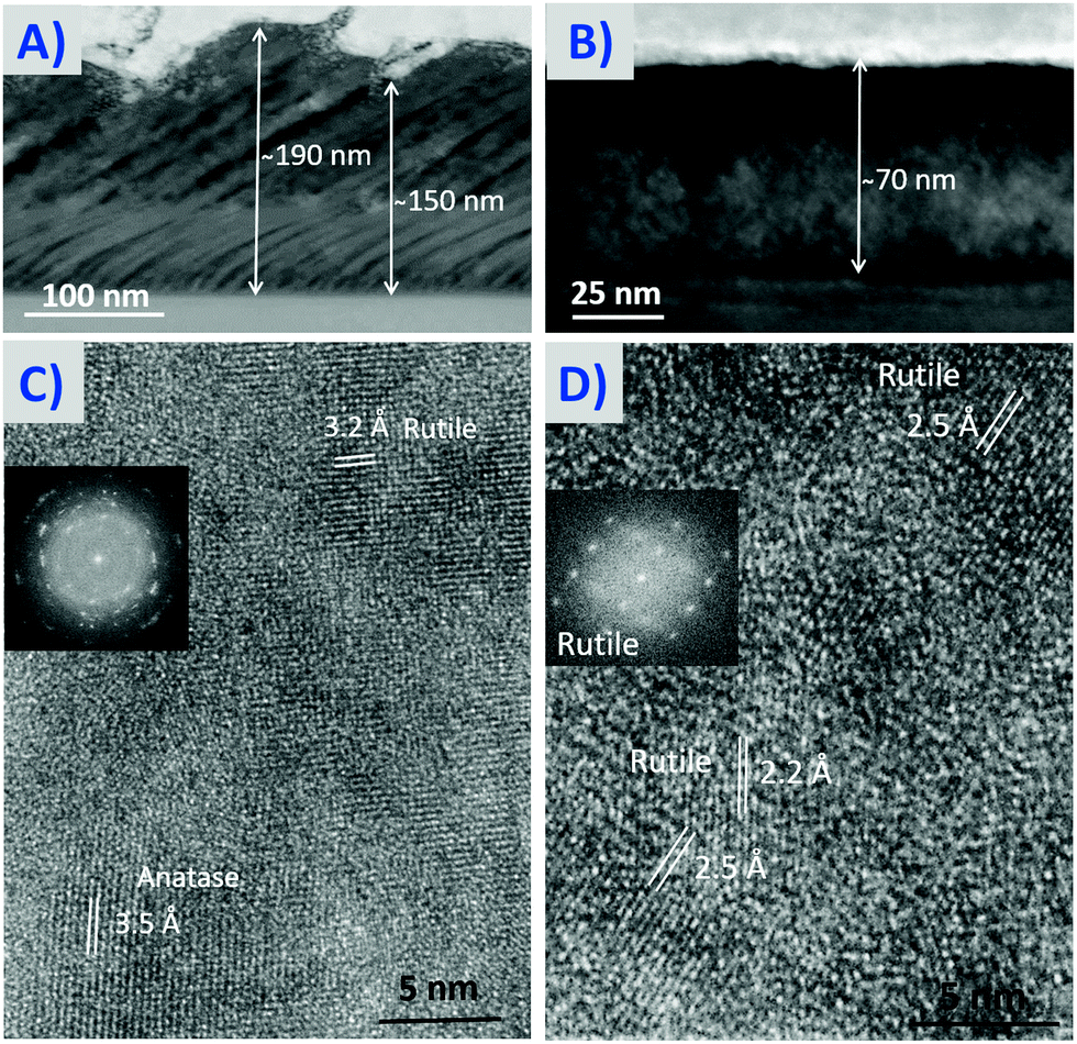 | ||
| Fig. 2 STEM and HRTEM analysis of the microstructure and crystallographic structure of the nanocolumnar and compact zones of sample TiO2(3.4)-180. (A) Cross section HAADF-STEM image of a lamella taken from a nanocolumnar domain. (B) Idem from a compact domain. Note the different magnification scales. (C and D) HRTEM images and the corresponding DDP's obtained at selected zones in (A) and (B). A careful observation of these images permits to identify crystallites with sizes varying from 5 to 15 nm in the nanocolumnar lamella and larger sizes in the compact one. The measured inter-planar distances are typical of a mixture anatase/rutile and rutile for the nanocolumnar and compact domains, respectively. | ||
AW simulation and experimental characterization of oscillatory behavior
The nanostructuring, crystallographic and pattering effects found in the AW-assisted TiO2 thin films deposited by MS (Fig. 1 and 2) should respond to piezoelectric lattice oscillations and/or electrical surface polarization processes resulting from the AW propagation through the piezoelectric plate substrate. A possible interplay between these substrate phenomena and the deposition process has been checked numerically through a 3D frequency-domain finite element model (FEM) simulation of the excited substrate, and experimentally by laser-Doppler vibrometry analysis of the deposited sample. Fig. 3A shows selected FEM simulations38 of both the AW amplitude field modulation and the local variations of surface electric potential for two close-by driving frequencies (for details about the simulation procedure see Section 3). The amplitude field distribution shows patterns in the form of front lines separated by distances in the order of 0.5–1 mm, i.e., similar to the TiO2 domains size. Interestingly, magnitude of oscillations amplitude and mode shape strongly vary with frequency (e.g., oscillations up to 4.5 nm occur for ω = 3.4200 MHz and less than 2.0 nm for ω = 3.4700 MHz, for a more complete set of results see Fig. S5, ESI†). Similarly, the model predicts a gradual electrical potential decrease from one chip side to the other and strong local modulations in local voltage with differences in the order of tenths of volts between adjacent zones of 0.5 to 1 mm size. Interestingly, although voltage difference at adjacent domains does not vary significantly with frequency, the electrical potential pattern is affected by this parameter and depicts either an aligned or a more scattered distribution at ω = 3.4200 MHz and ω = 3.4700 MHz, respectively. It is also remarkable that potential pattern is symmetric/antisymmetric in y-/x-direction, whilst the amplitude field is symmetric in both, x- and y-directions. It should be also noted that besides frequency, slight variations in chip geometry, mechanical clamping or material properties lead to noticeable changes in the simulated electric potential and amplitude field distributions. It is expected that all these factors will also affect film pattern distribution and that, therefore, much care is required for experimental reproducibility.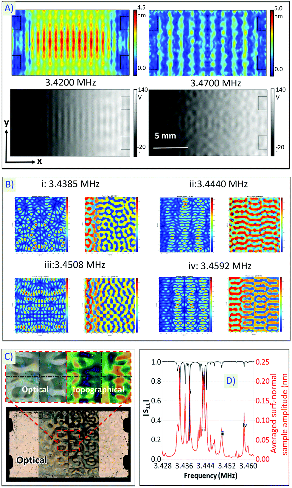 | ||
| Fig. 3 (A) FEM simulation of the amplitude (full coloured maps) and electrical field potential (grey maps) variations along the piezoelectric plate for two different frequencies, as indicated. (B) Selected maps of amplitude (left) and phase (right) distributions measured for sample TiO2(3.4)-180 at selected resonance frequencies. (C) Topography and optical images of the deposited TiO2 thin film with an enlargement of the centre to highlight the symmetry in the patterned film. (D) Plot of measured reflecion coefficient |S11| and area-averaged surface-normal displacements vs. AC excitation frequency (selected frequencies of resonant peaks i–iv correspond to those of the maps in Fig. 3B). | ||
Clues to determine whether the AW efficiently activates the piezolectric system after the deposition of a thin film was obtained by laser-Doppler vibrometry analysis of the AW propagation in sample TiO2(3.4)-180. Fig. 3B shows that, although AW amplitude and phase shift distributions depend on frequency, map features always have a similar size of 0.5–1 mm. Moreover, in agreement with the simulations in Fig. 3A for the bare substrate, AW amplitude maps are always symmetric in x- and y-directions, while phase maps are antisymmetric/symmetric in x-/y-directions (see a more complete set of results in Fig. S6, ESI†). The comparison of the amplitude and phase shift maps with the sample topography distribution in Fig. 3C, this latter characterized by antisymmetric and symmetric contrasts along the x- and y-directions, suggests that phase rather than amplitude is the most critical parameter controlling the electrical potential distribution. Sample TiO2(3.4)-180 was further characterized by vectorial network analysis (VNA). Fig. 3D shows two plots representing, respectively, the dispersion with frequency of the electrical reflection coefficient |S11| and the area-averaged surface-normal displacement amplitudes, these latter taken from Fig. 3B and Fig. S6 (ESI†). The two curves depict narrow-banded resonance peaks defining the optimal driving frequencies of plate wave modes. They also confirm that AWs efficiently propagate through the piezoelectric substrate after the deposition of a thin film on its surface, although modifications in resonant conditions during the deposition process cannot be excluded and might account for the observed thin film in-depth inhomogeneity.
Patterned growth mechanism
The previous analysis of the Lamb-type standing AWs, generated to assist the MS deposition of TiO2 thin films, shows that they are characterized by time dependent mechanical deformations extending through the whole lattice and an associated electrical surface polarization potential distribution, due to the inverse and direct piezoelectric effects, respectively.9 Theoretically both phenomena might contribute to induce the found patterned modulation of thin film nanostructure, thickness and optical properties. Various experiments, inducing the 2D densification pattern characteristic of sample TiO2(3.4)-180, however, disregard that transfer of mechanical energy and momentum from atom lattice oscillations to ad-species is a critical factor. Additional experiments showed that the interaction of the excited substrate with a plasma phase is a requirement for the observed patterned growth. This was firstly proved upon realizing that sample e-TiO2(3.4)-180, obtained under the assistance of AW by electron beam evaporation and therefore in the absence of plasma,39 presented an extended homogeneous nanocolumnar microstructure but no patterning (see Fig. S2-d, ESI†). In addition, in another experiment consisting of the AW assisted MS deposition on a piezoelectric substrate half coated with a thin metal layer (50 nm Ti), we found that the deposited TiO2 film appeared homogenously deposited onto the metallic part, but depicted a 2D patterned distribution on the pristine surface side (see Fig. S7, ESI†). Since the former occurred in a zone where the substrate potential was effectively shielded by the thin metal layer, we concluded that the intervention of the uneven polarization potential distribution generated on AW excited substrates (cf., Fig. 3A) is, besides the presence of a plasma, another requirement for the patterned growth.To account for these evidences, we propose that main patterning factor involves the electrostatic interaction between the charged species existing in the plasma sheath40 and the uneven local electrical potential distribution developed at the surface of the AW excited substrate. The scheme in Fig. 4 qualitatively describes our proposal for the interaction principles involved in the AW-assisted patterned deposition of plasma thin films. According to this scheme, the kinetic energy and local density of Ar+ ions in the plasma sheath40 would be modified when electrostatically interacting with the oscillating negative polarization appearing at the Lamb wave anti-node zones of substrate. As a result, the local fields at the substrate will induce an extra acceleration/focusing effect onto the sheath ions. In this way, the focussed ion impingement on the growing film, will induce an additional compaction in these zones. According to classical plasma sheath models,41 sheath potential follows well the variations of AC electrode bias potentials when ωτ ≤ 1 (ω frequency of applied field, τ ion transit time through the sheath, this latter depending on plasma pressure among other working parameters). For the gas pressures utilized to induce the plasma in our MS experiment, this condition is fulfilled for frequencies of few MHz, i.e., within the AC range used to induce the AWs in our experiment. It must be remarked though, that this would not be necessarily the case for other frequencies, working pressures and/or plasma electron densities. In that case, plasma sheath potential would not vary following the MHz changes in surface polarization and ions would not be so efficiently accelerated/focussed towards the substrate. We must also note, that a mechanical energy and momentum transfer from oscillating substrate lattice atoms to the ad-species cannot be excluded on the basis of the previous experiments. Crystallization effects or differences in the size and distribution of nanocolumns as those visible in Fig. S1 (ESI†), might be related with this type of energy transfer mechanism.
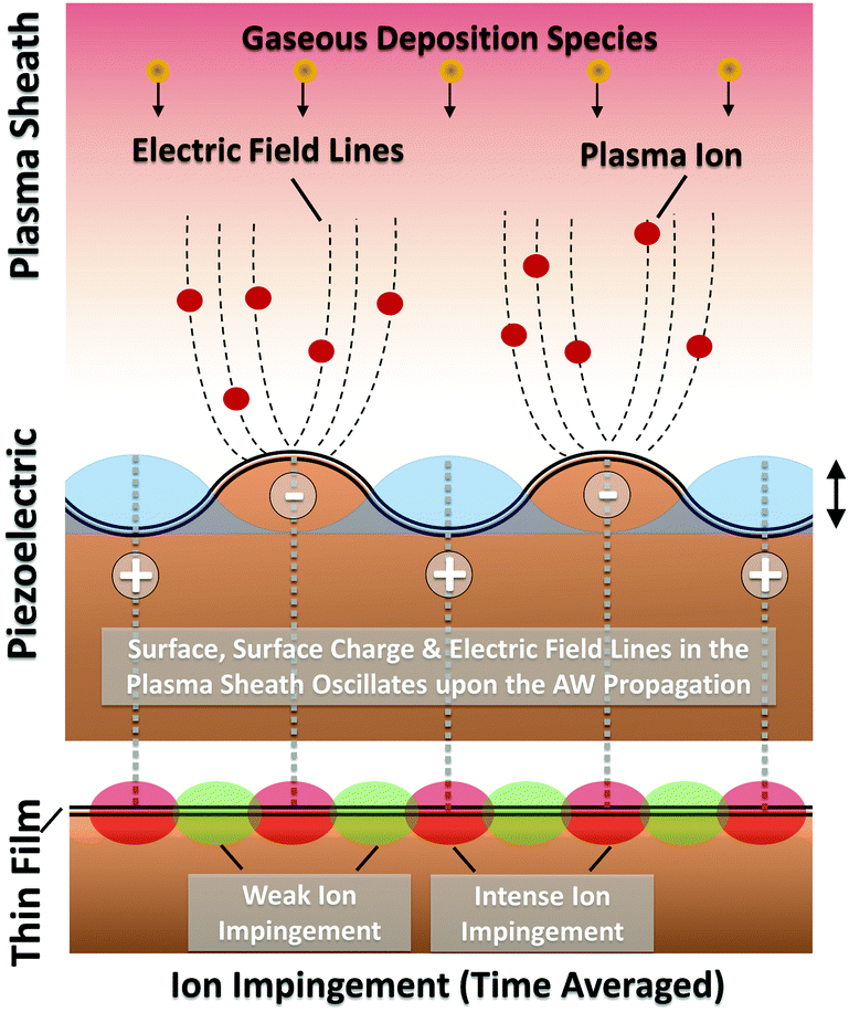 | ||
| Fig. 4 Scheme of the surface potential polarization model proposed to account for submillimeter zone densification of a dielectric thin film grown by AW-assisted MS. The standing AW produces the mechanical deformation of given zones (anti-nodes) of the substrate. In these zones, due to the direct piezoelectric effect, an alternating surface potential develops at MHz range frequencies. The alternating potential polarization of the surface modifies the plasma sheath, focussing and accelerating the positive Ar+ plasma ions towards these substrate zones during the negative polarization period, provided that the condition ωτ ≤ 1 is fulfilled.41 The net averaged effect of this local oscillatory change in surface potential is the ion beam densification of the film at the zones corresponding to the anti-nodes of the standing AW (red spots in the scheme), while no significant densification occurs at the node zones (green spots in the scheme) where no surface polarization occurs. | ||
In support of the interaction mechanism depicted in Fig. 4 to account for the patterned densification of the TiO2 thin films, we can claim other known phenomena involving the interaction between electrically heterogeneous substrates and plasma sheaths. This is the case, for example, of the irregular plasma sheath developed at metal–insulator lateral junctions,42,43 the plasma formation and alignment of carbon nanotubes,44 or the generation of plasmas by the so-called piezoelectric transformers.27,28 Also related with the local densification resulting from the model proposed in Fig. 4 is the known large area thin film densification occurring when biasing a substrate during MS deposition or under the bombardment with accelerated ions provided by an external source during Ion Beam Assisted Deposition (IBAD).45,46 Film densification has been also observed in Ar+ ion bombarded OAD thin films.47 The crystallization of TiO2 thin films, well-known to occur when assisting their growth with ion beams,36,37 further supports the involvement of ion beam effects in the crystallization phenomena reported in Fig. 2 for sample TiO2(3.4)-180.
Tailoring the patterned growth of thin films: case examples
The AW assisted MS deposition methodology offers many options for film patterning and nanostructuration as illustrated by various experiments where thin film morphology, structure and pattern distribution could be tailored through the adjustment of deposition conditions and AW operating parameters. To demonstrate these possibilities, herein, we show results on: (i) the MS deposition in a normal geometry; (ii) the OAD deposition of very thin films, and (iii) the usage of higher AC frequencies to excite higher harmonics. In addition, these experiments provide further support to the interaction mechanism responsible for the patterning process schematically described in Fig. 4.AW-assisted thin film growth in a normal MS configuration
The confocal and topography micrographs in Fig. 5A of sample N-TiO2(3.4)-390, grown in a normal MS configuration, shows a shallower patterned microstructure with domain sizes similar to those in Fig. 1A, but much smaller height differences between valley and hill regions, as deduced from its confocal topography map in Fig. 5A. SEM plane-view micrographs in Fig. 5B and TEM cross section micrographs in Fig. 5C reveal that film domains are rather compact, with less differences in nanostructure than between the nanocolumnar and compact zones in sample TiO2(3.4)-180 (cf., Fig. 1D). This is an expected result because MS films deposited in a normal configuration are already compact and, unlike the OAD thin films, not much additional 2D patterned densification is expected to be induced in thin films deposited in this geometrical configuration. Yet, despite the amorphous character of un-heated MS TiO2 films grown without AW assistance, crystallization of sample N-TiO2(3.4)-390 can be deduced from their HRTEM images (not shown) and the DDP's reported as insets in Fig. 5C. This crystallization supports a specific activation induced by the AWs that can be attributed to ion bombardment effects.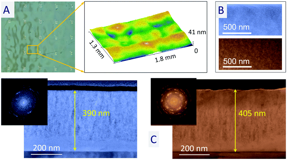 | ||
| Fig. 5 Analysis of sample N-TiO2(3.4)-390 grown in a normal configuration under the assistance of AWs. (A) Confocal image and topography maps (note the different z scales in each case). (B) SEM normal micrographs of compact (top) and porous (bottom) patterned zones. (C) TEM cross-section micrographs of compact (left) and porous (right) zones. Insets show the DDP's diagram in each case. | ||
AW-assisted growth of very thin OAD films
Fig. 6A shows confocal and topography micrographs for sample TiO2(3.4)-60. Clearly, these images reveal a surface pattern with domain sizes similar to those of sample TiO2(3.4)-180, indicating that patterning and local densification occur since the earlier stages of deposition. The in-plane SEM micrographs in Fig. 6B show that the valley regions are compact, while the hill regions are nanostructured and porous. This is confirmed by the TEM cross section images in Fig. 6C, while the DDP's reported as insets reveal that only an incipient crystallization into anatase and/or rutile has occurred in this very thin film. A poor crystallization at the earlier stages of AW-assisted deposition agrees with the observation in sample TiO2(3.4)-300 of a reduced crystallization close to the substrate (see Fig. S3, ESI†) and suggests that crystallization may progress during deposition, likely due to local increases of temperature and/or propagation of spikes provoked by ion bombardment.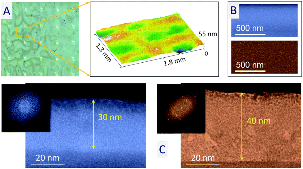 | ||
| Fig. 6 Analysis of sample TiO2(3.4)-60 grown in an OAD configuration under the assistance of AWs. (A) Confocal image and topography maps (note the different z scales in each case). (B) SEM normal micrographs of compact (top) and porous (bottom) patterned zones. (C) TEM cross-section micrographs of compact (left) and porous (right) zones. Insets show the DDP's diagram in each case. | ||
Tailoring the pattern size: thin film growth with higher AW frequencies
Lamb-type waves can be excited in LiNbO3 substrates at various resonance frequencies. To prove the effect of harmonic frequency on film growth, we deposited TiO2 exciting the piezoelectric substrate at 10.2791 MHz.48 Assuming the same acoustic velocity, the period of AW features generated at this frequency is expected to be around 3 times smaller than at ∼3.4 MHz. In other words, a patterned microstructure with smaller compact and porous/nanostructured domains of approximately 200–400 μm size should be obtained in this case. Confocal topography maps in Fig. 7A confirm this prediction, while SEM micrographs in Fig. 7B show that the microstructure of valley and hill regions present the expected nanocolumnar and compact microstructures already devised at lower frequencies. Crystallization into anatase and rutile was also proved by HRTEM (not shown) and electron diffraction analysis of this sample (cf., Fig. 7C). Overall, this experiment proves that pattern size can be modified playing with the frequency (and therefore periodicity) of the AW utilized to assist the deposition of the films.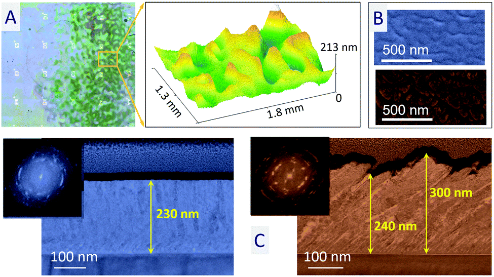 | ||
| Fig. 7 Analysis of sample TiO2(10.4)-180 grown in an OAD configuration under the assistance of AWs at higher frequency. (A) Confocal image and topography maps (note the different z scales in each case). (B) SEM normal micrographs of compact (top) and porous (bottom) patterned zones. (C) TEM cross-section micrographs of compact (left) and porous (right) zones. Insets show the DDP's diagram in each case. | ||
Experimental and methods
Thin film deposition
TiO2 thin films were deposited by reactive magnetron sputtering (MS) in normal geometry (i.e. target and substrate in parallel positions) and in oblique angle deposition (OAD) configurations, this latter at an angle of 85° between the perpendiculars to the target and substrate surfaces (Fig. 8a). Specific conditions for the MS deposition can be found as ESI† S8. We must stress that deposition pressure and substrate distance may affect the mean free path of ions and the sheath thickness, which in turn condition the value of the ωτ parameter. One of the criteria for selecting the deposition parameters was to comply with this condition. Another that sputtered atoms do not become randomized before arriving to the substrate and may therefore give rise to the nanocolumnar structure typical of OAD tin films.49 Fully oxidized TiO2 thin films and equivalent growth rates of 1.9 nm min−1 and 0.7 nm min−1 were obtained in normal and OAD geometries, respectively. These growth rates were determined from cross section SEM micrographs taken for thin films grown on a silicon wafer placed besides the acoustic wave (AW) assisted piezoelectric substrates (see Fig. 8b). Distance between target and AW deposition device was kept at approximately 7 cm to ensure the immersion of the deposited film within the plasma generated around the MS target.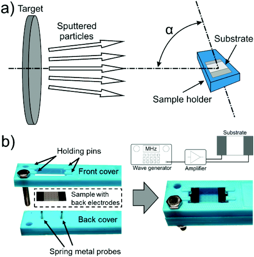 | ||
| Fig. 8 (a) Scheme of the deposition arrangement showing the definition of deposition angle and the possibility to rotate the sample holder in front of the magnetron sputtering target. (b) View of sample holder of the piezoelectric substrate before (left) and after (right) closing the device with a back cover prior to the experiment. Photographs include a view of the LiNbO3 substrates with the metal strips used as electrical contacts, the springs used as electrical connectors and the pins holding the substrate once the device is closed. Quartz and/or silicon substrates were placed beside the LiNbO3 substrate (at the location labelled “Front cover”). The scheme describes the electrical set-up used for RF excitation of piezoelectric plate. | ||
Film deposition was carried out simultaneously on a piezoelectric substrate (LiNbO3 substrate) under AW assistance (for comparison also without AW assistance) and, for reference purposes, on adjacent quartz and silicon substrate plates. The piezoelectric substrate consisted of a piece (1 cm × 2 cm) of a double-side polished LiNbO3 single crystal wafer (128° Y-cut) exposing the  crystallographic plane at the surface (Roditi International Corporation Ltd). Electrical contacts consisted of rectangular patches of 0.5 cm width and 1 cm length made of a Ti/Al bilayer of 5/295 nm thickness, structured via a common Lift-off technique employing electron beam evaporation. A specially designed sample holder was used for AW assistance during deposition. According to the scheme in Fig. 8b, the sample holder consisted of a frame made of an electrically insulating material. The LiNbO3 plate was floating inside a rectangular cavity made in the frame where it was held by four small pins coming from the frame while pushed by two thin metal headed springs acting as electrical contacts onto the Ti/Al bilayer electrodes. Metal contacts and thread wiring were protected from the plasma environment by an insulating back cover. This configuration made that, except for the pins and springs, no contact exists between piezoelectric substrate and frame, thus ensuring fixation and a negligible mechanical attenuation of the vibrating piezoelectric plate by the sample holder. Unlike other experimental arrangements where the LiNbO3 crystal was contacted with larger electrodes and/or kept by larger holding pins, the used set up provided a good reproducibility in the pattern distribution when repeating the deposition experiments. In addition, this design made it possible to place reference substrates of quartz and silicon in the proximity of the piezoelectric plate, at the same distance and deposition angles with respect to the MS target. To enable a precise adjustment of the deposition angle during the OAD experiments, the sample holder was fixed to a rotary rod and turned an angle α as indicated in Fig. 8a.
For comparative purposes, some experiments were also carried out by electron beam evaporation. In this case TiO2 thin films were deposited on the sample holder shown in Fig. 8 placed in an e-beam evaporation set-up. By these experiments, the AW actuated piezoelectric substrate was placed at the same deposition angle as for the MS deposition, although distance between target and substrate was adjusted to 50 cm. TiO, i.e. nominal titanium monoxide, was used as target material (note that the surface of pellets was likely more oxidized), while oxygen was dosed in the chamber up to a maximum partial pressure of 5 × 10⁻⁵ mbar to ensure a TiO2 stoichiometry for the deposited films. Evaporation rate at the substrate surface was adjusted to values similar to those determined for the MS experiments, e.g. approximately 1.2 nm min−1. Further details about the characteristics of e-beam evaporated TiO2 thin films deposited onto silicon and quartz substrates under an OAD configuration in the same set-up can be found in a previous publication.39
Thin film characterization
Physical properties, microstructure and crystallinity of the deposited films were determined by different characterization techniques including Optical Reflectometry with a focused light beam, Confocal Interferometric Microscopy, Scanning (SEM) and Transmission Electron Microscopy (TEM) together with electron diffraction, X-ray Diffraction (XRD), Raman spectroscopy, Digital Optical Microscopy, and Mechanical Profilometry. Experimental details about these characterization techniques are provided as ESI† S8.Acoustic wave excitation and characterization
A scheme of the electrical system used for AW excitation is included in Fig. 8b. The setup consisted of an RF signal generator (Agilent 8648A Synthesized RF generator (Keysight Technologies) followed by a High Power Amplifier ZHL-5W (Mini-Circuits)). The generated signal had 108 V peak to peak amplitude and a frequency around 3.4 and 10.4 MHz. Determination of exact resonant frequencies for the deposition experiments was done in two steps with the sample holder in air. Firstly, by a rough assessment consisting of the observation of the nebulization of a water droplet placed on the surface of the piezoelectric substrate while progressively changing the frequency. Then, a more accurate determination of resonance frequency was done measuring the maximum in conductance spectrum with an Impedance Analyzer HP-4294A (Keysight Technologies) working in the conductance mode in the range between 1 and 5 MHz. Once determined this resonant frequency, the sample holder was placed in the MS deposition chamber and experiments carried out as described above.Network analysis and resonant characteristics of the piezoelectric substrates covered with the thin films were carried out in air in the same holder device used for the deposition experiments, after taking it out from the deposition chamber. Vectorial network analysis (VNA) was carried out by S11 measurements with an Agilent 5081b VNA apparatus. Amplitude and phase mapping of the AW oscillation were collected with a laser Doppler vibrometer (UHF 120, Polytec GmbH) with temperature stabilization and drift correction. A multi-carrier signal consisting of 141 Fourier lines and an overall input voltage of 1 V was used for this purpose. Each measurement point was subjected to 5 times complex averaging. Data analysis was carried out using Matlab and Polytec File Access.
Acoustic wave simulation
To further investigate the acoustically-induced modulations of electric potential and total displacement field on the chip surface, 3D frequency-domain FEM simulations were carried out using COMSOL Multiphysics v5.5 on a custom workstation with 32 logical processors at 2.60 GHz operation frequency and 512 GB RAM (approx. 25 hours per simulation). By employing the solid mechanics module, a complete model of the system with estimated positions for the mechanical clamping, i.e. fix constrains, on a LiNbO3 substrate (with speed of sound of 3994 m s−1 and density of 4628 kg m−3) was generated and analyzed. To generate the intended waves propagating through and on the substrate, a harmonic voltage potential at 110 V was applied along equipotential surfaces mimicking the pattern of aluminium electrodes. For this purpose we used a coupled electrostatic module, at a range of operational frequencies (3.44 to 3.45 MHz at the step of 100 Hz), i.e. within the range used for the measurements and experiments. Based on the assumption that aluminium is almost a perfect conductor, the electrical signal was applied to equipotential plates. However, aluminium plates were included within the simulation to investigate the effect of their mechanical properties on mode shape and electrical field developed at the substrate surface. The coordinate axis of the tensor dataset (piezoelectric, stiffness and permittivity tensors) for z-normal oriented LiNbO338 was rotated 38° around the x-axis to represent the particular crystal orientation of the LiNbO3 substrate used experimentally. To precisely and accurately capture the physics involved in the AW excitation, a free tetrahedral mesh with a highly fine structure (minimum mesh size is 20 μm) near the edges was used. The number of freedom degrees solved was 1.883.666. To simulate the acoustic energy loss due to amplitude decay of the waves through and along the substrate, the model incorporated a mechanical damping of 0.001 and a dielectric loss of 0.01. Since this model was sufficient to clearly demonstrate the trends in electric potential and displacement modulations, the deposited TiO2 thin film was not considered in the calculations.Conclusions
The previous experiments prove that assisting the plasma deposition of thin films with AWs renders a patterned distribution of density, morphology and thickness, with compacted zones intermingled in other without observable densification and where domain size and distribution can be controlled through the adjustment of deposition parameters and AW properties. Crystallization at ambient temperature is another effect attributed to the activation by AWs. Since no pattering occurs without plasma, we propose that the interaction between the inhomogeneous electric field distribution generated on the piezoelectric substrate and the plasma sheath ions is the main energizing factor controlling the local densification effects. This fundamental discovery opens numerous new research opportunities. For example, we have proved that changing the acoustic driving frequency can be employed to modify the pattern size. However, shrinking the pattern size to micron or smaller ranges is yet to be proved. In earlier investigations, Takahashi et al.,29 using SAWs to assist the growth of ferromagnetic metal films, did not find any patterning, but a generalized film flattening and densification. Whether this relates to the high frequency of 45 MHz utilized in their experiments, the deposition of a metal instead of a dielectric material, the use of SAWs or the fulfillment of the ωτ ≤ 1 condition are open questions for future investigations.We believe that the pattering principles established here can be extrapolated to other conditions closer to practical applications where the piezoelectric plates might be substituted by piezoelectric films35,50 deposited on any kind of substrates, including polymers. Applications are thus devised for the fabrication of biomimetic or antifouling surfaces, as well as in photonics and microelectronics where controlled crystallization and tailored 2D-patterning of nanostructure of metal or dielectric films and/or multilayers would provide decisive processing advantages compared to the classical methods.
Conflicts of interest
There are no conflicts to declare.Acknowledgements
Authors thank the FEDER program through AEI-MICINN (PID2019-110430GB-C21) and the Junta de Andalucía (PAIDI-2020 through projects P18-RT-3480 and ref. 6079), the CSIC (2019AEP161, 201860E050), the H2020-EU.1.2.1-FET OPEN program (grant 899352, project SOUNDofICE and the EFRE InfraPro project ChAMP, for financial support. We recognize the support of Dr R. Poyato (ICMSE) for support by the realization of some experiments, that of Dr J Santiso (CiN2-CSIC) for exploratory XRD analysis and Dr A. del Campo (ICV-CSIC) by the Raman characterization.References
- J. Zheng, R. Yang, L. Xie, J. Qu, Y. Liu and X. Li, Adv. Mater., 2010, 22, 1451 CrossRef CAS.
- I. Petrov, P. B. Barna, L. Hultman and J. E. Greene, J. Vac. Sci. Technol., A, 2003, 2, S117 CrossRef.
- G. Abadias, E. Chason, J. Keckes, M. Sebastiani, G. B. Thompson, E. Barthel, G. L. Doll, C. E. Murray, C. H. Stoessel and L. Martinu, J. Vac. Sci. Technol., A, 2018, 36, 010801 CrossRef.
- D. W. Reagor and V. Y. Butko, Nat. Mater., 2005, 4, 593 CrossRef CAS.
- N. Wakiya, T. Kawaguchi, N. Sakamoto, H. Das, K. Shinozaki and H. Suzuki, J. Ceram. Soc. Jap., 2017, 125, 856 CrossRef CAS.
- W. G. Bae, H. N. Kim, D. Kim, S. H. Park, H. E. Jeong and K. Y. Suh, Adv. Mater., 2014, 26, 675 CrossRef CAS.
- Lithography, ed. M. Wang, InTech Publishing co, 2010 Search PubMed.
- S. Tawfi, M. De Volder, D. Copic, S. J. Park, C. R. Oliver, E. S. Polsen, M. J. Roberts and A. J. Hart, Adv. Mater., 2012, 24, 1628 CrossRef.
- J. L. Rose, Ultrasonic Guided waves in Solid Media, Cambridge University Press, 2014. ISBN 978-1-107-04895-9 Search PubMed.
- A. Darabi, A. Zareei, M. R. Alam and M. J. Leamy, Sci. Rep., 2018, 8, 29192-1 Search PubMed.
- A. V. Mamishev, K. Sundara-Rajan, F. Yang, Y. Du and M. Zahn, Proceedings IEEE 92, 2004, vol. 92, p. 808.
- B. Heinrich, Nat. Nanotechnol., 2018, 13, 769 CrossRef CAS.
- D. B. Go, M. Z. Atashbar, Z. Ramshani and H. C. Chang, Anal. Methods, 2017, 9, 4112 RSC.
- L. Y. Yeo and J. R. Friend, Annu. Rev. Fluid Mech., 2014, 46, 379 CrossRef.
- L. Zhou, J. He, W. Li, P. He, Q. Ye, B. Fu, P. Tao, C. Song, J. Wu, T. Deng and W. Shang, Nanolett., 2019, 19, 2627 CrossRef CAS.
- H. Zhao, S. Fan, Y. Chen, Z. Feng, H. Zhang, W. Pang, D. Zhang and M. Zhang, ACS Appl. Mater. Interfaces, 2017, 9, 40774 CrossRef CAS.
- B. Casals, N. Statuto, M. Foerster, A. Hernández-Mínguez, R. Cichelero, P. Manshausen, A. Mandziak, L. Aballe, J. M. Hernández and F. Macia, Phys. Rev. Lett., 2020, 124, 137202 CrossRef CAS.
- L. Shu, S. Ke, L. Fei, W. Huang, Z. Wang, J. Gong, X. Jiang, L. Wang, F. Li, S. Lei, Z. Rao, Y. Zhou, R. K. Zheng, Y. Xi, Y. Wang, M. Stengel and G. Catalan, Nat. Mater., 2020, 19, 605 CrossRef CAS.
- M. A. Khalid, A. Ray, S. Cohen, M. Manlio Tassieri, A. Demčenko, D. Tseng, J. Reboud, A. Ozcan and J. M. Cooper, ACS Nano, 2019, 13, 11062 CrossRef CAS.
- M. Eslamian, Prog. Org. Coat., 2017, 113, 60 CrossRef CAS.
- Y. Chen, X. Ding, S. S. Lin, S. Yang, P. H. Huang, N. Nama, Y. Zhao, A. A. Nawaz, F. Guo, W. Wang, Y. Gu, T. E. Mallouk and T. J. Huang, ACS Nano, 2013, 7, 3306 CrossRef CAS.
- H. Sazan, S. Piperno, S. M. Layani, S. Magdassi and H. Shpaisman, J. Colloid Interface Sci., 2019, 536, 701 CrossRef CAS.
- Z. Ma, J. Guo, Y. J. Liu and Y. Ai, Nanoscale, 2015, 7, 14047 RSC.
- P. Delsing, et al., The 2019 surface acoustic waves roadmap, J. Appl. Phys. D: Appl. Phys., 2019, 52, 353001 CrossRef CAS.
- K. Ostrikov, E. C. Neyts and M. Meyyappan, Adv. Phys., 2013, 62, 113 CrossRef CAS.
- A. Alvarez-Laguna, T. Magin, M. Massot, A. Bourdon and P. Chaber, Plasma Sources Sci. Technol., 2020, 29, 025003 CAS.
- H. Itoh and S. Suzuki, Plasma Sources Sci. Technol., 2014, 23, 054014 CrossRef.
- M. J. Johnson and D. B. Go, J. Appl. Phys., 2015, 118, 243304 CrossRef.
- M. Takahashi, H. Shoji and M. Tsunoda, J. Magn. Magn. Mater., 1994, 134, 403 CrossRef CAS.
- U. Diebold, Surf. Sci. Rep., 2003, 48, 53 CrossRef CAS.
- F. D. Lin and S. W. Boettcher, Nat. Mater., 2014, 13, 81 CrossRef CAS.
- A. Kubacka, M. Fernandez-García and G. Colon, Chem. Rev., 2012, 112, 1555 CrossRef CAS.
- A. Barranco, A. Borrás, A. R. González-Elipe and A. Palmero, Prog. Mater. Sci., 2016, 76, 59 CrossRef CAS.
- M. M. Hawkeye, M. T. Taschuk and M. J. Brett, Glancing angle deposition of thin films: engineering the nanoscale, Wiley series in Materials for Electronic & Optoelectronic Applications, Wiley 2014 Search PubMed.
- M. Cao and J. Jiang, Surf. Innovations, 2016, 4, 180 CrossRef.
- B. M. Pabon, B. J. I. Beltran, G. Sanchez-Santolino, I. Palacio, J. Lopez-Sanchez, J. Rubio-Zuazo, J. M. Rojo, P. Ferrer, A. Mascaraque, M. C. Muñoz, M. Varela, G. R. Castro and O. Rodrıguez de la Fuente, Nat. Commun., 2015, 6, 6147 CrossRef CAS.
- J. Jia, H. Yamamoto, T. Okajima and Y. Shigesato, Nanoscale Res. Lett., 2016, 22, 324 CrossRef.
- G. Kovacs, M. Anhorn, H. E. Engan, G. Visintini and C. C. W. Ruppel, IEEE Symposium on Ultrasonics, Honolulu, HI, USA, 1990, vol. 1, 435.
- L. Gonzalez-Garcia, J. Parra-Barranco, J. R. Sanchez-Valencia, A. Barranco, A. Borras, A. R. Gonzalez-Elipe, M. C. Garcia-Gutierrez, J. J. Hernandez, D. R. Rueda and T. A. Ezquerra, Nanotechnology, 2012, 23, 205701 CrossRef.
- J. P. Sheehan, N. Hershkowitz, I. D. Kaganovich, H. Wang, Y. Raitses, E. V. Barnat, B. R. Weatherford and D. Sydorenko, Phys. Rev. Lett., 2013, 111, 075002 CrossRef CAS.
- T. Panagopoulos and D. J. Economou, J. Appl. Phys., 1999, 85, 3435 CrossRef CAS.
- E. V. Barnat and A. Hebner, J. Appl. Phys., 2004, 96, 4762 CrossRef CAS.
- Y. Fu, P. Zhang, J. P. Verboncoeur, A. J. Christlieb and X. Wang, Phys. Plasmas, 2018, 25, 013530 CrossRef.
- T. Hirata, N. Satake, G. H. Jeong, T. Kato and R. Hatakeyama, Appl. Phys. Lett., 2003, 83, 1119 CrossRef CAS.
- I. Utke, P. Hoffmann and J. Melangailis, J. Vac. Sci. Technol., B, 2008, 26, 1197 CrossRef CAS.
- W. Ensinger, Surf. Coat. Technol., 1998, 99, 1 CrossRef CAS.
- J. B. Sorge, M. T. Taschuk, N. G. Wakefield, J. C. Sit and J. M. J. Brett, J. Vac. Sci. Technol., A, 2012, 30, 021507 CrossRef.
- A. R. Rezk, J. R. Friend and L. Y. Yeo, Lab Chip, 2014, 14, 1802 RSC.
- A. Garcia-Valenzuela, R. Alvarez, V. Rico, J. Cotrino, A. R. Gonzalez-Elipe and A. Palmero, Surf. Coat. Technol., 2018, 343, 172 CrossRef CAS.
- M. Akiyama, T. Kamohara, K. Kano, A. Teshigahara, Y. Takeuchi and N. Kawahara, Adv. Mater., 2009, 21, 593 CrossRef CAS.
Footnote |
| † Electronic supplementary information (ESI) available: Nanostructure of sample without AW excitation; UV-vis spectra of thin films withough AW excitation; XRS and Raman analysis of AW assisted thin films; in-depth TEM analysis of thin films; FEM calculations of AW propagation; amplitude and phase maps of AW excited thin films; AW assisted thin film deposited on a substrate half covered with a metal; additional experimental and methods details. See DOI: 10.1039/d0mh01540g |
| This journal is © The Royal Society of Chemistry 2021 |