
 Open Access Article
 This Open Access Article is licensed under a
 Creative Commons Attribution 3.0 Unported Licence
A highly selective electron affinity facilitated H2S sensor: the marriage of tris(keto-hydrazone) and an organic field-effect transistor†
Saravanan
Yuvaraja‡
 a,
Veerabhadraswamy Nagarajappa
Bhyranalyar‡
b,
Sachin Ashok
Bhat
b,
Sandeep Goud
Surya
*a,
Channabasaveshwar Veerappa
Yelamaggad
*b and
Khaled Nabil
Salama
*a
a,
Veerabhadraswamy Nagarajappa
Bhyranalyar‡
b,
Sachin Ashok
Bhat
b,
Sandeep Goud
Surya
*a,
Channabasaveshwar Veerappa
Yelamaggad
*b and
Khaled Nabil
Salama
*a
aSensors lab, Advanced Membranes and Porous Materials Center, Computer, Electrical and Mathematical Science and Engineering Division, King Abdullah University of Science and Technology (KAUST), Thuwal, 23955-6900, Kingdom of Saudi Arabia. E-mail: sandeep.surya@kaust.edu.sa; khaled.salama@kaust.edu.sa
bCentre for Nano and Soft Matter Sciences (CeNS), Jalahalli, Bengaluru 560 013, India. E-mail: yelamaggad@cens.res.in
First published on 28th September 2020
Abstract
Conjugated polymers (CPs) are emerging as part of a promising future for gas-sensing applications. However, some of their limitations, such as poor specificity, humidity sensitivity and poor ambient stability, remain persistent. Herein, a novel combination of a polymer–monomer heterostructure, derived from a CP (PDVT-10) and a newly reported monomer [tris(keto-hydrazone)] has been integrated in an organic field-effect transistor (OFET) platform to sense H2S selectively. The hybrid heterostructure shows an unprecedented sensitivity (525% ppm−1) and high selectivity toward H2S gas. In addition, we demonstrated that the PDVT-10/tris(keto-hydrazone) OFET sensor has the lowest limit of detection (1 ppb), excellent ambient stability (∼5% current degradation after 150 days), good response–recovery behavior, and exceptional electrical behavior and gas response reproducibility. This work can help pave the way to incorporate futuristic gas sensors in a multitude of applications.
New conceptsA biological nose is a consortium of multiple sensing and signal conditioning elements, which are key in identifying airborne analytes. An important element of the biological nose that transduces the binding and identification of airborne molecules is olfactory receptor neuron (ORN). Here, we tried to mimic ORN with the help of an organic electronic device that consists of a biodegradable polymer and a monomer. Our device is a p-type organic field-effect transistor (OFET) that not only operates in accumulation mode but also makes use of a synergistic heterostructure that detects H2S gas selectively. The top layer of the heterostructure is realized with a novel monomer, tris(keto-hydrazone), which is both porous and contains H2S specific functional groups. On the other hand, the bottom layer is the active channel layer of the OFET and essentially plays a key role in altering the transduction output. Thus, the proposed synergistic combination helps to preconcentrate the H2S molecules, initiates acid–base chemical reaction and alters the majority hole carriers of the channel region in the OFET device. This work highlights the use of hydrazones for the first time in OFET sensors and provides a new route to realize advanced analyte sensing applications. |
Introduction
Hydrogen sulfide (H2S) is a colorless, corrosive, malodorous, and poisonous gaseous substance often encountered in hot-springs and during the production of crude-petroleum products, as well as while refining natural gases.1,2 At low concentration levels, exogenous H2S inhalation improves neurological functions and cardiac conditions.3 High doses (< 10 ppm) cause eye irritation and fatigue, and exposure to levels > 100 ppm results in severe neurological damage and cardiovascular conditions.4,5 Thus, the methodical development of effective sensors to monitor H2S gas levels is of paramount importance and can have a significant impact on our daily lives. The standard tool used in workplaces to sense the presence of toxic gases is the detector tube6,7 due to its calibration-free measurements, low-cost and high efficiency.6 However, serious drawbacks such as a slow response, temperature sensitivity, low shelf life and low accuracy may lead to false alarms and other detrimental conditions.7 Alternatively, the pellistor-type sensor is considered to be a reliable candidate for the detection of combustible gases,8 where the catalytic activity oxidizes the target gas, resulting in a voltage change.9 This was followed by using ultrasonic gas detectors that are extensively used as gas-leak detectors where the device operation is based on a frequency-sensing principle.10 By contrast, the accurate determination of volatile organic compounds (VOCs) requires a photoionization-based detector (PID) as an alternative choice.11 Unlike others, the semiconductor-based gas/VOC sensors have gained increased attention because of the flexibility in tuning the electronic properties of the semiconducting materials leading to improved specificity.12–14Conjugated polymers (CPs) provide innumerable opportunities to realize versatile interactions with environmental analytes.10,15 Diketopyrrolopyrrole-(DPP-)based CP semiconductors in particular are considered to be promising materials for sensing as a result of their tunable bandgap, good ambient stability, interactive functional groups and flexible electronic properties.16–22 Furthermore, combining the versatile DPP molecules with rigid structures such as naphthalene, thiophene and their analogous moieties results in donor–acceptor (D–A) architectures with homogenous crystal stacking and strong pi–pi intermolecular interactions.18,20,22 Recently, many research groups have successfully integrated the DPP-based D–A polymers on organic field-effect transistor (OFET) platforms to sense NH3,23–26 NO2,27–29 H2S30,31 and various VOC molecules.20 Though DPP-based polymers are suitable candidates to sense harmful gases at the ppb level, the major setbacks of such sensors are their poor air stability and the aging effect, both of which lead to poor sensing performance.20,22 Therefore, there is still a huge demand to develop high-performance organic gas sensors that can overcome the above challenges and meet the requirements of practical applications. On the other hand, hydrazones (R1R2C = NNHR) are widely recognized as functional organic materials for various applications.32–34 They uniquely possess both basic and acidic characteristics owing to the presence of functional groups.32,35 These versatile characteristics enable their wide use in sensing anions/cations, medical biotechnology, molecular switching, sensing applications and so on.36,37
As the tailored attributes of both CPs and hydrazones can effectively enable them to realize a fully functional solid-state sensor device, we thus propose a novel DPP copolymer with a thiophene donor block (PDVT-10)/tris(keto-hydrazone) heterostructure-based OFET device that is both CMOS compatible and highly sensitive to H2S. The realization of the conceived organic (polymer–monomer) heterostructure gives rise to excellent charge transport properties of the ultra-thin PDVT-10 film to be combined with copious gas-binding active sites in the form of secondary amine functional groups of the porous tris(keto-hydrazone) film. The intrinsic strong basic character of the secondary amine group facilitates the intense association of tris(keto-hydrazone)s with weakly acidic H2S molecules. When compared to a pristine PDVT-10 OFET device, the developed PDVT-10/tris(keto-hydrazone) heterostructure sensors exhibit an exceptional 64-fold increase in sensitivity toward H2S gas, with an excellent selectivity when operating at room temperature. With the help of UV-Vis spectroscopy, surface and cross-section Kelvin probe force microscopy (KPFM) techniques, we have proposed a sensing mechanism to illustrate the improved sensing performance of the PDVT-10/tris(keto-hydrazone) heterostructure toward H2S gas.
Results and discussion
Detector design and operating principle
The development of gas-sensor technology with capabilities such as high sensitivity, good selectivity and quick response and recovery has gained importance in recent years. This kind of electronic gas sensor is favored over other potential counterparts due to its industry-ready CMOS-compatibility to achieve easy integration into circuits, large-scale manufacturing capability and increased yield. The top view of our OFET gas sensor with specially designed gas-absorbent membranes is shown in Fig. 1 (center). The fabrication process of this sensor is schematically represented (Fig. S5, ESI†). In this sensor, the highly doped n-type silicon (n++Si) platform serves as both a physical support and a bottom gate terminal. Using the solution processing technique (Fig. S5, ESI†), we have deposited the DPP-based D–A PDVT-10 organic semiconductor on the surface of electrodes, ensuring that it inherits good charge transport behavior. The chemical structure of this material can be seen in Fig. 1a. The challenging part of this process is to design an organic absorbent receptor layer with the desired features and to integrate it on the OFET device platform. As a rule of thumb, the elements used to design efficient gas-absorbent layers to realize better-sensing performance are (i) gas-molecule-selective functional groups with (ii) good semiconducting properties and (iii) good stability. In the case of a bilayer configuration, the preferred elements will have (i) appreciable chemical compatibility among layers, (ii) good porous structures to improve gas absorption and (iii) good stability under various ambient conditions. Some of the strategies employed to realize better-sensing performance using DPP-based OFET sensors include optimization of film thickness,16,17,20,38 tuning the porous structures to improve the surface reactivity,18,20,39,40 blending the polymers with materials (such as graphene oxide,39 MoS2,39 polystyrenes,39 PBA39 and MOF22) and attaching functional groups (sulfur-based motif,41 siloxane,39 butoxycarboxyl,39 tetraethyl glycol,16 thymine42 and naphthalene20) to the side chain of polymers. However, major disadvantages include their poor stability under humidity and bias stress and the resultant failure to exhibit reproducible and reliable gas-sensing performance. To overcome these challenges, we have designed our OFET layers by combining an amine-based monomer tri(keto-hydrazone) compound (top gas-absorption layer) supported on top of a highly stable organic semiconductor whose chemical structure can be seen in Fig. 1b. Followed by this, the transfer characteristics of both PDVT-10 (D1) and tris(keto-hydrazone)/PDVT-10 heterojunction (D4) OFET devices are presented in Fig. 1c. Using a CMOS-compatible approach, we have successfully fabricated a miniaturized OFET sensor whose size measured around 5.0 mm × 5.0 mm, which exactly fits on top of the forefinger (Fig. 1d). As shown in Fig. 1e, initially, the incoming gas molecules being absorbed by the amine-based compound (tris(keto-hydrazone)) leads to a chemical reaction, thereby changing the device parameters. To prove this hypothesis, we have presented detailed studies on the surface characterization, device sensing performance, environmental stability and sensing mechanism.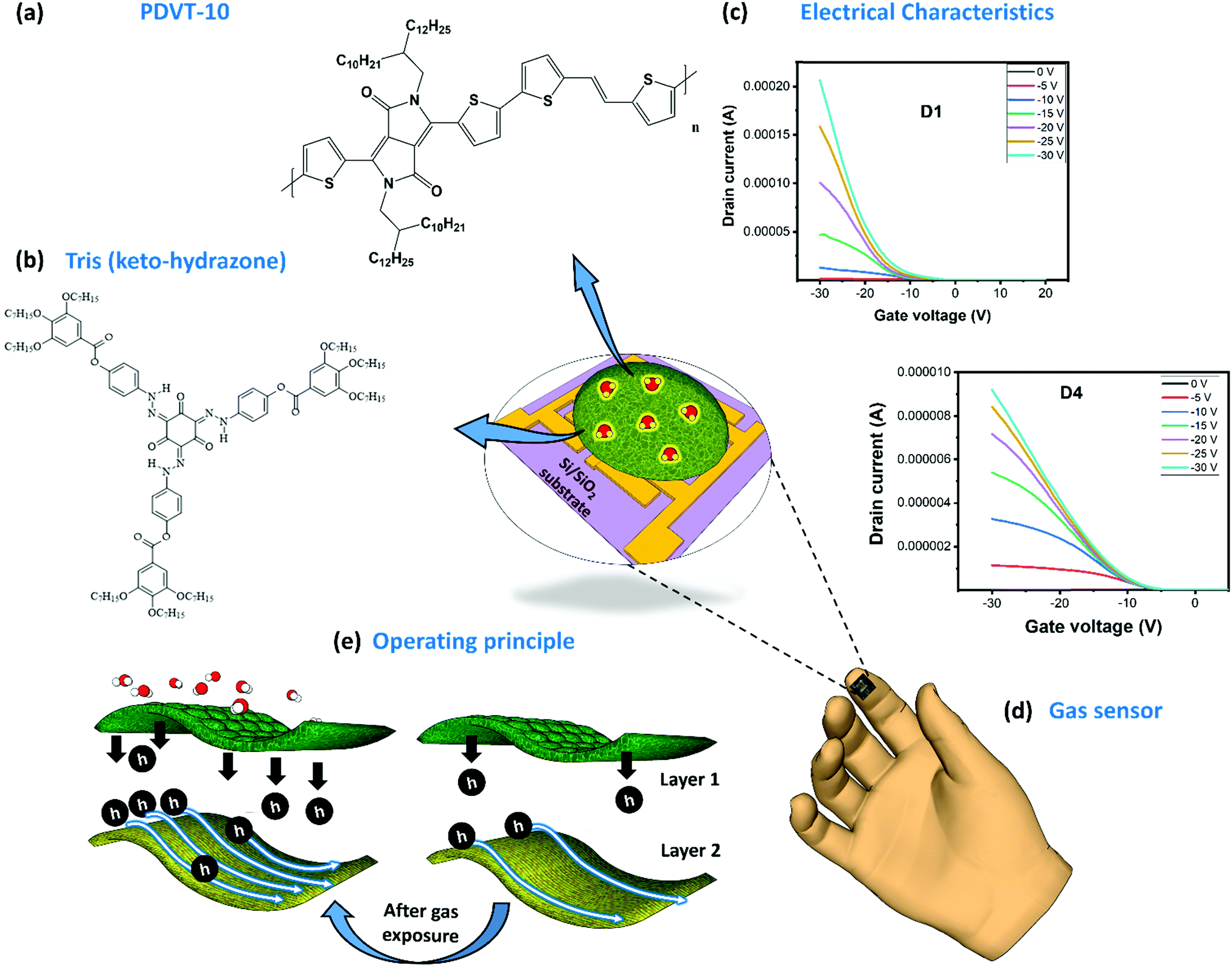 | ||
| Fig. 1 PDVT-10/tris(keto-hydrazone) OFET design and sensing principle (center). Schematic representation of an OFET device on a Si/SiO2 substrate. Chemical structure of (a) the PDVT-10 bottom charge transport layer and (b) the tris(keto-hydrazone) top gas absorption layer. (c) Electrical characteristics of PDVT-10 (D1) and PDVT-10/tris(keto-hydrazone) OFET devices. (d) The total size of our device is 5 mm × 5 mm, exactly fitting on the tip of the forefinger. (e) The operating principle of the gas absorption layer before, during and after gas exposure. Layer 1 and Layer 2 define the functions of hydrazones and PDVT-10 materials, respectively. | ||
Surface characterization
The polymer material PDVT-10, hereafter referred to as M1, was procured, and three new tris(keto-hydrazone) monomers, namely, HDN4, HDN6 and HDN7, abbreviated respectively as M2, M3 and M4, were synthesized and characterized (see the Experimental section, ESI†). The material M1 comprises DPP and thiophene-vinyl-thiophene (TVT) functional groups, acting respectively as electron donors (D) and electron acceptors (A). Compounds M2, M3 and M4 possess nine n-butyloxy, n-hexyloxy and n-heptyloxy tails at the periphery, respectively. The molecular structures of M3 and M4 are presented (Fig. S7, ESI†). The surface properties of all the materials were probed using field emission scanning electron microscopy (FESEM), atomic force microscopy (AFM) and Kelvin probe force microscopy (KPFM).The corresponding morphologies of M1, M2, M3 and M4 were obtained through FESEM imaging (Fig. 2), and a detailed explanation is provided in (SN1, ESI†). Furthermore, the thickness of M2, M3 and M4 was probed using the AFM technique (Fig. S8, ESI†), and the corresponding average thickness and roughness are summarized in (Table S1, ESI†). It is apparent from the table that the thicknesses of M2, M3 and M4 are about 168 nm, 233 nm and 235 nm, respectively. As expected, the surface of the ultrathin M1 film is smooth with a mean roughness measured around 1 nm (Fig. 2i). Similar to the thickness trend of M2, M3 and M4 materials observed before, their corresponding mean roughness extracted from the AFM images (Fig. 2j–l) follows the same pattern. We posit that the observed decrease in roughness along with the increase in peripheral alkoxy chains enables M4 to gain an edge in terms of electronic properties over other hydrazone homologues. With the help of the KPFM technique, the electronic properties of all the materials (M1 to M4) were explored. Initially, the mean contact potential difference (CPD) value of M1 was extracted from the recorded potential map measured at around −0.23 V (Fig. 2m). By contrast, the polarity of CPD obtained for all the hydrazones is positive (Table S1, ESI†). A brief explanation regarding the method followed to obtain the CPD for each material (M1–M4) and how it was used to calculate the materials’ work function, helpful for future discussion, is provided in (SN2, ESI†). Importantly, as can be seen in Fig. S14, ESI,† there is a significant increase in the CPD values rising from 1.01 V (M2) to 1.853 V (M4). We can infer that M4 with a higher mean CPD has more availability for surface free electrons, hence leading to better electron donor behavior when compared to its M2 and M3 counterparts. It is a well-known fact that an increased number of valence electrons results in strong repulsive forces, causing steric effects that lead to an increase in the surface energy of the system. Eventually, this leads to an increase in the surface potentials of M2, M3 and M4 due to the corresponding increase in chain lengths, which is observed in KPFM as well. The relation between the steric effect and surface potential is illustrated in the inset of Fig. S14, ESI.† In summary, we have witnessed interesting surface properties in both M1 and M4 materials, which aligns with the requirements to achieve promising sensing performance.
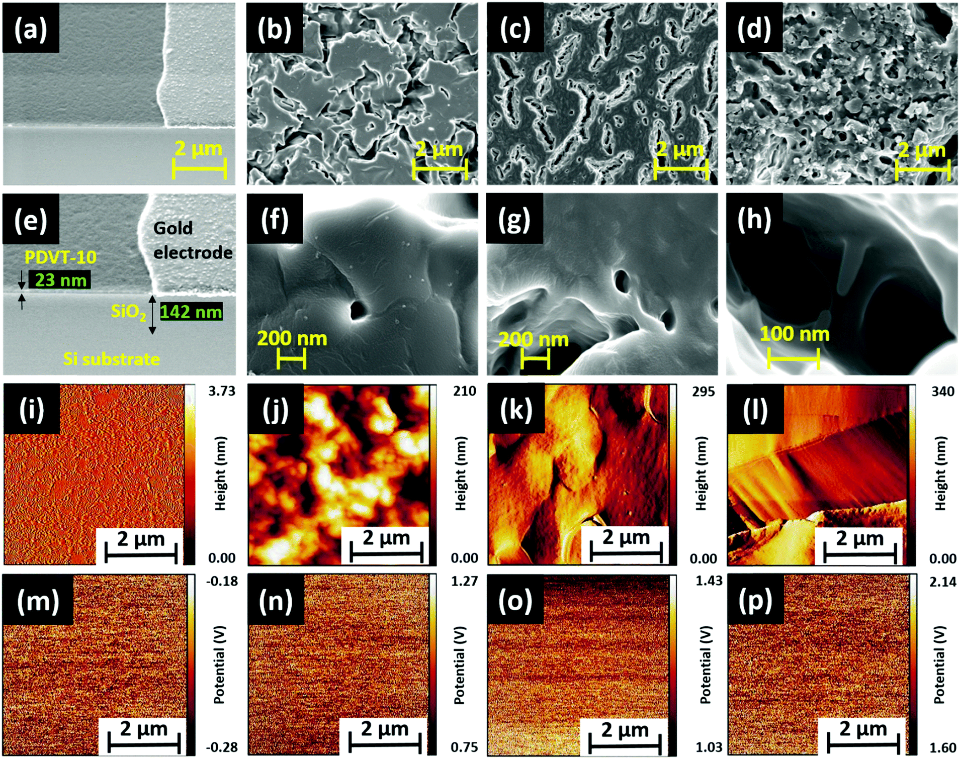 | ||
| Fig. 2 Surface characterization of gas absorbent layers. (a–d) Low-magnification field-emission scanning electron microscopy (FESEM) images. (e–h) High-magnification FESEM images. (i–l) Atomic force microscopy (AFM) surface topography images. (m–p) Kelvin probe force microscopy (KPFM) images of gas absorbent materials PDVT-10 (M1) (a, e, i, m), HDN4 (M2) (b, f, j, n), HDN6 (M3) (c, g, k, o) and HDN7 (M4) (d, h, l, p). | ||
Device characterization
Electrical characterization was performed for all the fabricated OFET devices, and the performance of these devices was assessed with two categories of characterization, transfer and output characteristics. From these behavioral curves, some of the important transistor parameters, namely, threshold voltage (Vth), current ratio (Ion/Ioff), subthreshold swing (SS), transconductance (Gm) and mobility (μ) were considered to evaluate the electrical characteristics of the fabricated OFET devices. First, we have recorded the transfer curves for all the devices, including the bare OFET device (D1) and tris(keto-hydrazone) coated devices (D2–D4); the corresponding plots are presented in Fig. 3a. The transfer curves were obtained by sweeping gate-source voltage (VGS) = +10 V to −30 V for different drain–source voltage (VDS) = 0 V to −30 V step levels, based on optimized biasing conditions. As can be seen in Fig. 3a(i), after applying the required biasing conditions, device D1 not only shows textbook-like curves, but also turns “ON” at a negative gate sweeping region close to zero bias. The latter outcome highlights the formation of a small/negligible depletion layer in the channel region at the semiconductor/dielectric interface part. This resulted in the generation of a notable current level of around 195 μA at VGS = VDS = −30 V. Like the D1 device, hydrazone based OFET devices D2, D3 and D4 were also subjected to similar gate and drain biasing conditions. The corresponding transfer curves are recorded and graphically illustrated in Fig. 3a(ii)–(iv). Similarly, the output behavior of all the devices was obtained by sweeping drain-source voltage (VDS) = 0 V to −30 V for different gate-source voltage (VGS) = 0 V to −30 V step levels. Fig. 3b shows the ideal output curves, in which cut-off, linear and saturation regions are distinguishable. In the case of transfer characteristics, a decline of around two orders of magnitude in the drain current levels is observed after introducing the hydrazones on top of PDVT-10 OFET devices. This outcome can be attributed to the excess electron transfer from hydrazones leading to the depletion of majority hole carriers in the PDVT-10 channel region. The charge transfer process between PDVT-10 and hydrazones is discussed in the device sensing mechanism section. The comparison of transfer curves of D2, D3 and D4 devices clearly shows that there is an increasing trend in drain current, where the D4 device produced 9 μA drain current at VGS = VDS = −30 V, which is roughly three times greater than the D2 counterpart. From the transfer curves of D1–D4, the previously mentioned transistor parameters were calculated using the standard device physics relations (SN3, ESI†), and the corresponding values are tabulated in Table S2, ESI.† The error bar graph of the transistor parameters for all the devices is presented in Fig. S15, ESI.† In comparison to the results of the hydrazone-based OFET devices, parameters such as Vth and SS exhibit a decreasing trend, whereas the remaining parameters show an opposite trend from devices D2 to D4. An OFET device with desired features, which include a low threshold voltage, a high current ratio, a low subthreshold swing, a high transconductance and a high charge carrier mobility, is ideally required to realize good sensing performance. Among the tested devices, D1 and D4 OFETs exclusively satisfy the performance requirements of the standard device, with D4 also displaying high-quality gas sensing performance.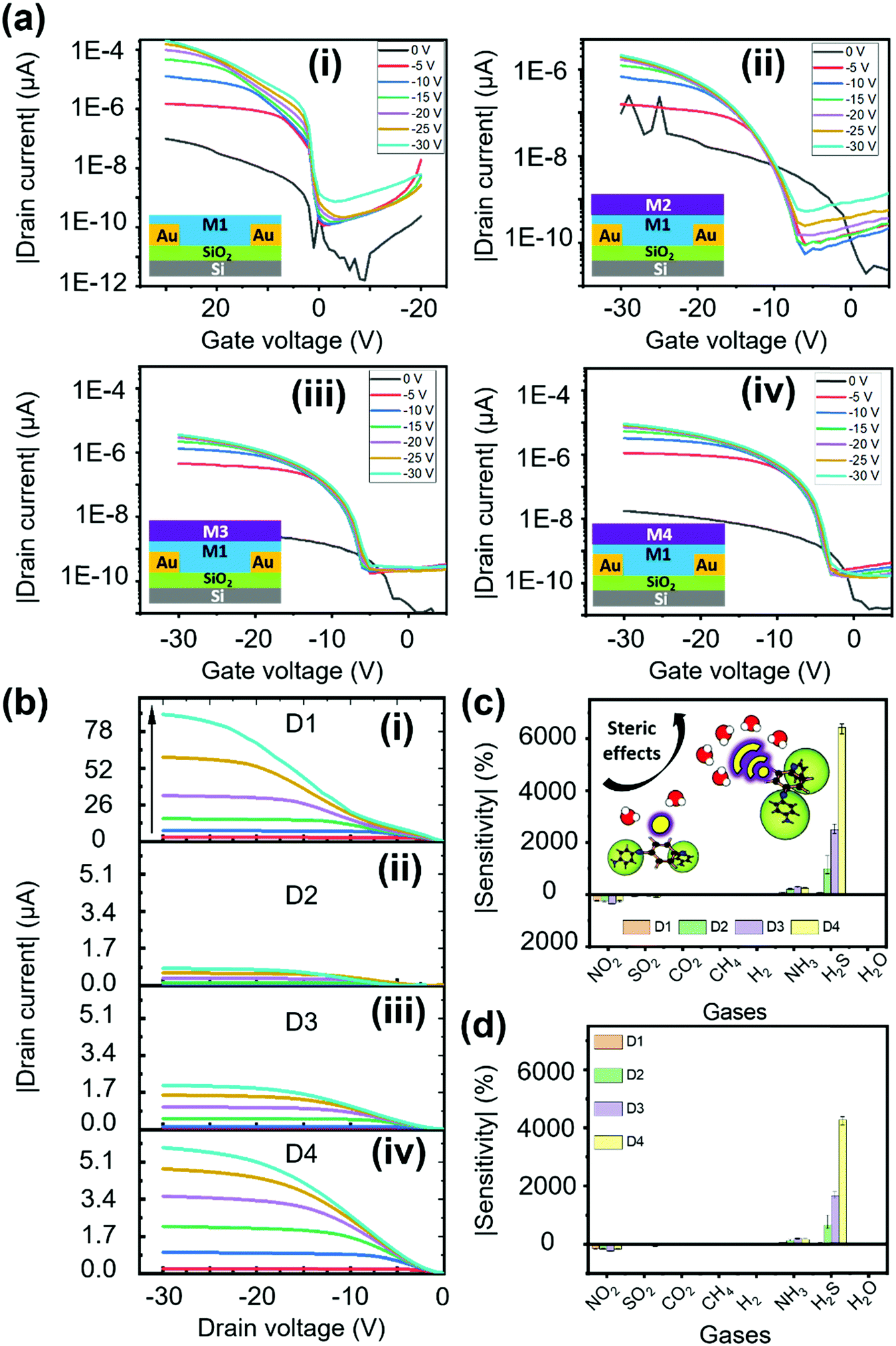 | ||
| Fig. 3 PDVT-10/tris(keto-hydrazone) OFET device electrical characteristics. (a) Transfer (ID–VGS) and (b) output (ID–VDS) behavior of (i) pristine M1 [D1], and (ii) M1/M2 [D2], (iii) M1/M3 [D3] and (iv) M1/M4 [D4] OFET devices. The insets of (a) show the 2-D schematic diagram of all the tested OFET devices. Selectivity behavior of all the OFET devices (D1–D4) tested against oxidizing (50 ppm), reducing (50 ppm) and moisture analytes, wherein the sensitivity data are calculated from the (c) transfer (current from the linear region) and (d) output characteristics (current from the saturation region). | ||
Sensing device performance
In a series of studies performed using D1–D4 OFET devices in the presence of toxic analytes we understood their sensing performance. Initially, the D1 device was exposed to both oxidizing and reducing gases at a fixed 50 ppm concentration under an inert N2 atmosphere, and the corresponding transfer characteristics were recorded (Fig. S16, ESI†) using a VGS = +20 to −30 V at VDS = −30 V biasing condition. From the linear region of these curves, the current changes were extracted to obtain the sensitivity of D1 to different tested gases. As depicted in Fig. 3c, D1 tends to show a reasonable sensitivity of around 235%, with a moderate selectivity toward NO2 gas. As anticipated, the D1 device exhibited poor sensing performance toward H2S gas due to the poor porosity and absence of desired functional groups to facilitate gas–receptor binding activity. Based on the hypothesis of material synthesis and observations made from the surface and electrical characterization results, the hydrazone-based devices (D2–D4) might outperform their D1 counterpart in sensing H2S gas. Therefore, the transfer characteristics of devices D2–D4 to the same set of gases were recorded under similar biasing conditions (Fig. S17–S19, ESI†). The sensitivity of devices D2–D4 to the gases is presented in Fig. 3c. Interestingly, the D4 OFET device showed unprecedented changes, measuring a sensitivity to H2S of around 6400%, which was greater than those of the other tested devices, accompanied by a negligible response to NO2 gas. The observed H2S response is attributed to the improved surface binding affinity, contributed by strong steric effects due to the presence of higher-order alkoxy side chains, as illustrated in the inset of Fig. 3c. We have also plotted the selectivity data (Fig. 3d), wherein the sensitivity percentage was calculated using the drain saturation current extracted from output characteristics. By comparing the results from Fig. 3c and d, we can infer that there is a significant decrease in the overall sensitivity of devices operating in a saturation region. It is thus essential to operate the device in a linear region to realize the maximum sensing performance. Subsequently, the majority of the stability and transient analysis studies were performed on D4 to understand its characteristics with respect to H2S gas.Before characterizing the D4 device for further understanding its sensing characteristics, it is vital to probe the hysteresis effect of the D4 device over time. During this experiment, the device under testing was biased at VGS = +20 to −30 V, and VDS = −30 V. From Fig. S20 (ESI†), we can infer that D4 exhibited negligible hysteresis. Followed by this, as shown in Fig. 4a, the D4 device was exposed to different H2S gas concentrations at room temperature in a N2 atmosphere from 5 ppb to 25 ppm, and the corresponding changes in current were obtained by biasing the device at VGS = VDS = −30 V. We can make the device completely recover back to the baseline level by heating to 55 °C in an inert atmosphere for different durations ranging from 160 s to 370 s depending on the gas concentrations. With the help of the widely used root mean square (RMS) technique, we have found that our D4 device possess a theoretical limit of detection of around 1 ppb (Fig. S21, ESI†).
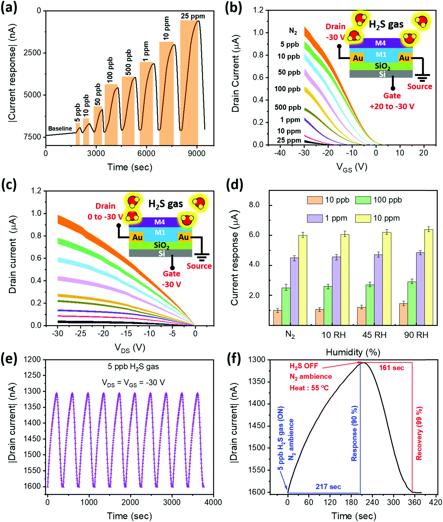 | ||
| Fig. 4 D4 OFET sensor performance. (a) Transient analysis of a D4 OFET device with different concentrations of H2S gas, ranging from 5 ppb to 25 ppm. (b) Transfer and (c) output characteristics of the D4 OFET device toward different H2S gas concentrations from 5 ppb to 25 ppm. (d) Effect of humidity (varied from 10% and 90% RH) on the sensing performance of the D4 OFET device. (e) Repeatability behavior of the D4 OFET H2S sensor tested at 5 ppb H2S concentration repeated for 10 cycles. (f) Response and recovery curve obtained from the D4 OFET device in the presence of 5 ppb H2S gas. | ||
Following this, the transfer and output characteristics of the D4 device toward various concentrations of H2S were recorded (Fig. 4b and c) to highlight the relation between the gas interaction and transistor parameters. The device architecture and the associated bias connections followed during gas testing are illustrated in the insets of Fig. 4b and c. Before exposing the device to the toxic gas, the total flow rate of N2 carrier gas was maintained at 200 sccm for 5 min, and the corresponding transfer and output curves from the device were recorded, as can be seen in Fig. 4b and c. Moreover, we have rigorously applied the same flow rate and exposure time of N2 gas before exposing the device to the target gas molecules. In Fig. 4b and c, the curves of error bar data, taken from 5 devices to ensure reproducibility, illustrate that the devices have allowed around 1 μA current at VGS = VDS = −30 V. Subsequently, after toxic gas exposure, we have used the same N2 gas flow rate to allow the device to completely recover. However, the exposure time duration differs and it solely depends on the exposed gas concentrations. From these figures, it is clear that the employed pre-exposure conditions are standard and hence resulted in reproducible device behaviour. From Fig. S22, ESI,† we can observe that the threshold voltage tends to increase with increasing concentration. This might be due to the ions (HS−), generated due to the interaction between the hydrazones and H2S molecules,34 that are transferred to the M1 material. These transferred HS− ions tend to trap the holes (q) in the conduction channel via electrostatic attraction, which causes a significant positive shift in the threshold voltage (VTH). This is confirmed with the help of the mathematical relation between the charges (q) in the channel and VTH, as can be seen in eqn (1).
| VTH = (CoxVG − qet)/Cox | (1) |
This phenomenon was further confirmed by the results of charge carrier mobility and conductivity behavior (transconductance), which sharply declines with the gas concentrations (Fig. S22, ESI†). Moreover, the provided ESI† depicts the increasing trend of a subthreshold swing with gas concentrations, possibly linked to the proposed phenomenon. The concept and characterization evidence for the proposed phenomenon are elaborated in the following sections.
We have also studied the effects of different humidity (RH [%]) backgrounds on the current response of the D4 device toward 10 ppb, 100 ppb, 1 ppm and 10 ppm H2S gas (Fig. 4d). In a N2 atmosphere, the current change of the D4 device was measured to be around 1.0 μA, 2.5 μA, 4.3 μA and 6.1 μA in the presence of 10 ppb, 100 ppb, 1 ppm and 10 ppm gas concentrations, respectively. After increasing the humidity of the testing chamber to 90% RH, the current response toward 10 ppb, 100 ppb, 1 ppm and 10 ppm gas concentrations increased by 16%, 12.5%, 8% and 3%, respectively (Fig. S23, ESI†). The results indicate a significant effect of high humidity (90% RH) on the sensitivity of the device toward the gas concentrations (ppb range). The humidity effect becomes negligible, however, while sensing the target gases at higher concentration.
We repeated the exposure and recovery cycles 10 times using 5 ppb H2S gas to probe the robustness and repeatability of the device (D4). As shown in Fig. 4e, the tested device shows an excellent repeatable nature, maintaining the same level of sensitivity. We further zoomed-in to probe the time taken by the device to complete one response and recovery cycle (Fig. 4f). The result shows that our device takes approximately 217 seconds to reach a 90% current response level from the baseline. After saturation, we turned off the target H2S gas without disrupting the flow of N2 gas and operated the heater to mildly heat the device at 55 °C, allowing the device to return (99%) to the baseline within 161 seconds. In summary, the D4 device exhibited excellent H2S sensing performance and outperformed the other tested devices. In addition, we have explored the stability of our sensors against bias stress, and ambient and humidity conditions (Fig. 5). A detailed discussion on the results is reported in (SN4, ESI†). The outcome of the stability study highlights the exceptional ambient, humidity and bias stress stability of our D4 sensors.
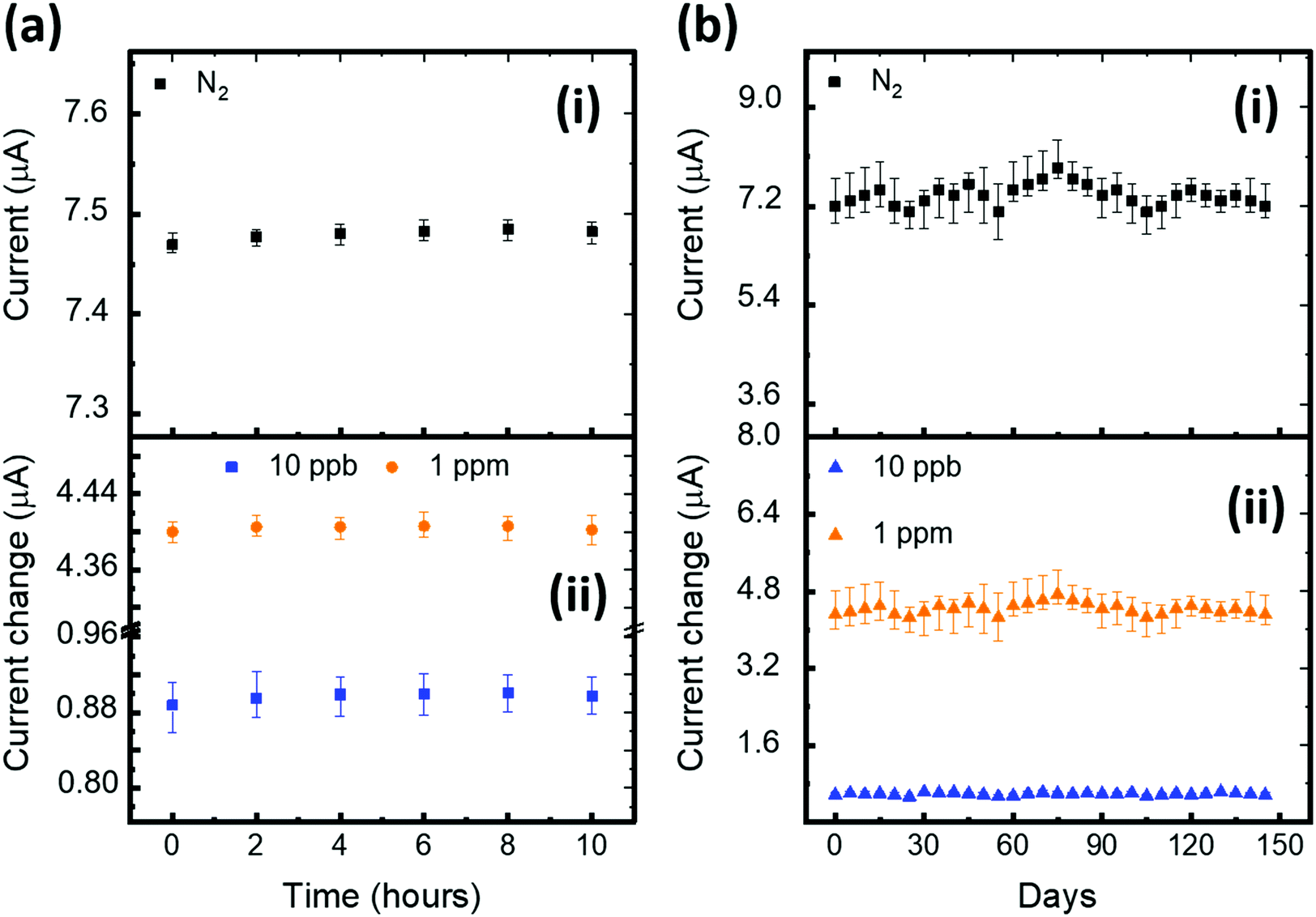 | ||
| Fig. 5 Stability studies of the D4 OFET H2S sensor. (a) Bias stress stability characteristics tested over a period of 10 hours and (b) five-month ambient stability of the D4 OFET sensor toward (i) a N2 inert atmosphere and (ii) in the presence of 10 ppb and 1 ppm H2S gas. | ||
Gas sensing mechanism
Here, we have used spectroscopic and microscopic characterization to unveil the mechanism underlying the improved sensing mechanism of the D4 device. Initially, the H2S capturing ability of the M4 material was studied qualitatively. The images of EDX mapping of the pristine and H2S-exposed M4 thin-film are shown in Fig. 6a and b, respectively. While the elemental color mapping of the pristine film confirms the presence of nitrogen solely as contemplated (Fig. 6a), the profile of the exposed film reveals the existence of both nitrogen and sulfur elements (Fig. 6b). This implies that M4 readily captures/absorbs H2S molecules. The exposed thin-film remains unaltered after prolonged storing under ambient conditions and even upon flushing with a stream of O2 gas (Fig. 6c). However, interestingly, the absorbent could be rejuvenated at a relatively low temperature, namely around 50–55 °C, as evidenced by the EDX mapping image (Fig. 6d).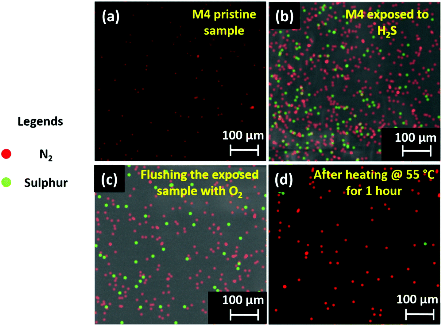 | ||
| Fig. 6 Surface optical characterization of the M4 material. Energy-dispersive X-ray spectroscopy (EDX) map of (a) a pristine M4 thin film sample, (b) a H2S-exposed M4 sample, (c) a H2S-exposed M4 sample flushed with O2 gas, and (d) the complete removal of absorbed H2S gas molecules from an M4 sample after heating at 55 °C for 1 hour. Red and green dots represent the presence of N2 and sulfur elements on the surface of the M4 thin film. | ||
In addition, we are keen to explore the effect of H2S gas molecules on the surface electronic properties of the gas-absorbent layers. Initially, we have hypothesized a gas-absorption process that takes place on the surface of gas-sensing layers. The detailed information can be seen in SN5, ESI.† Followed by this, the electron distribution and energy levels (bandgap) of the highest occupied molecular orbital (HOMO) and lowest unoccupied molecular orbital (LUMO) for pristine M4, and the complex (M4:H2S) formed by its intermolecular association with the H2S molecule, were acquired by Density Functional Theory (DFT)-based theoretical calculations. Calculations were performed with ORCA 4.0 software using the B3LYP function in conjunction with the def2-TZVP basis set. Fig. 7(a–d) depict the HOMO and LUMO electron distribution and energy values. The electron densities and the HOMO–LUMO band gaps are different for the pristine sample and the complex formed. For sample M4, the HOMO orbitals localize on the conjugated long arms (Fig. 7b), and the LUMO orbitals delocalize on the entire central core where the amino groups (nitrogen atoms) exist (Fig. 7a). The HOMO and LUMO energy levels are respectively −5.1 and −2.9 eV. Thus, the bandgap of compound M4 before is 2.2 eV. For the complex, wherein compound M4 associates with the H2S molecule, the electron density of the HOMO orbitals varies drastically, as can be seen from Fig. 7d. The electron density of the HOMO is more delocalized as compared to that of M4; it shifts substantially towards the H2S present at the arms, indicating the strong interaction of H2S with M4, whereas the electron density of the LUMO persists on the core (Fig. 7c); the HOMO and LUMO have energy values of 5.3 and 3.3 eV. Thus, the bandgap of the complex is ∼2.0 eV, which is comparatively lower than that noted for the pristine sample. Thus, the intermolecular association of H2S with M4 will vary the HOMO value of the pristine sample from 5.1 eV to 5.3 eV, which is also evident from the comparison of images of the HOMO. This result agrees with the general observation that any segment that can withdraw electrons will vary the HOMO level notably. It is also clear that the electron density in the HOMO of M4 is more delocalized when it interacts with the H2S molecule. Based on these results, it is reasonable to suggest that the interaction of H2S with M4 alters electron density, and hence affects the bandgap. Thus, the intermolecular interaction of H2S with M4 is electronic rather than simple van der Waals attraction. To support the observed simulation results, we have studied the relation between the gas interaction and the surface potential of both M1 and M4 materials using surface KPFM characterization; a detailed explanation is provided in SN6, ESI.† From the obtained surface potential results, we have calculated the change in CPD (%) and plotted it against the corresponding gases, as shown in Fig. 7j. This figure indicates that the M4 material showcases exceptional CPD changes in the presence of H2S gas, which matches our selectivity study results and the concept illustrated in Fig. 7d. As expected, M1 shows excellent selectivity toward NO2, but the CPD change of M1 due to H2S is nowhere near as high as the CPD response of the M4 material (Fig. 7j). In addition, when compared to NO2 and NH3 interferants, the M4 material has shown exceptional CPD (%) change in response to H2S gas, aligning with our previous inferences.
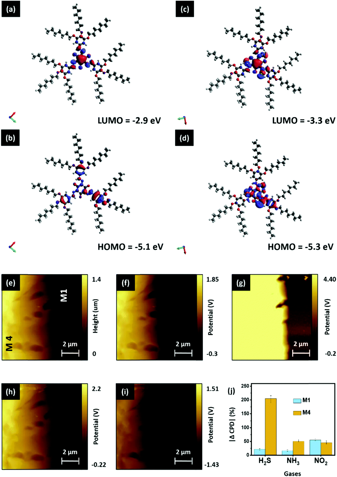 | ||
| Fig. 7 Optimized electron distribution/density diagrams of HOMOs (bottom) and LUMOs (top) for the pristine HDN-7 (a, b) and the complex (HDN-7:H2S) (c, d) formed by an intermolecular association of HDN-7 with H2S. Surface KPFM characterization of gas-absorbent layers in the presence of gas. (e) Topography image of M4 (left) and M1 (right) materials and the contact potential difference (CPD) potential map of M1 and M4 materials (f) before exposure and in the presence of (g) H2S (1 ppm), (h) NH3 (200 ppm) and (i) NO2 (100 ppm) gas molecules. (j) Relation between the change in CPD (Δ CPD) of M1 and M4 materials extracted in the presence of different tested gases. | ||
Next, we explored the charge transfer process between the M1 and M4 materials to understand the overall sensing process in the D4 device. With the help of energy band theory and the results of prior studies, we have attempted to hypothesize the concept of a charge transport process between the materials (M1 and M4). A detailed explanation related to the energy band properties of both M1 and M4 materials can be seen in SN7, ESI.† With the help of the calculated HOMO and LUMO levels, we have outlined the energy band diagram of the gas-absorbent layers (M1 and M4), as shown in Fig. 8a. As shown in Fig. 8a, while M4 makes physical contact with the underlying M1 material, this results in the formation of a depletion layer at the interface. This interface is formed by the diffusion of dominant charge carriers from the corresponding materials.43 Consequently, the electrons tend to diffuse and occupy the LUMO state in the p-type M1 material region.43–46 Furthermore, Fig. 8a shows the formation of a p–n heterojunction between M1 (p-type) and M4 (n-type), and the depletion region is formed at the M1/M4 interface. The variation of charge density at the depletion layer has a direct bearing on the drain current of an OFET device.47 In the current study, the variation in the active layer has brought about changes in drain current that can be attributed to variance in the dissipation of charge (electron) from M4 into the M1 (holes) layer. M4 has a higher surface charge/electron density (observed from KPFM), demonstrated by its higher drain current, which arises due to the ineffective recombination of holes and electrons.47,48 This generally occurs when the electron does not effectively penetrate the depletion layer and enter the M1 layer. This observation can be ascribed to the number of carbon atoms in the tail, to which the steric crowding contributes significantly. Furthermore, the observation may be attributed to the presence of bulky long alkoxy chains48,49 present in M4, as compared with the other two systems (M2 and M3). This physically hinders the electron movement, thereby causing less movement across the depletion layer and rendering a higher drain current output, both of which enhance the sensitivity. When compared to the reported room-temperature operating H2S sensors, as can be seen in Table S3, ESI,† our sensor (D4) has the record lowest detection limit reported to-date of 1 ppb.
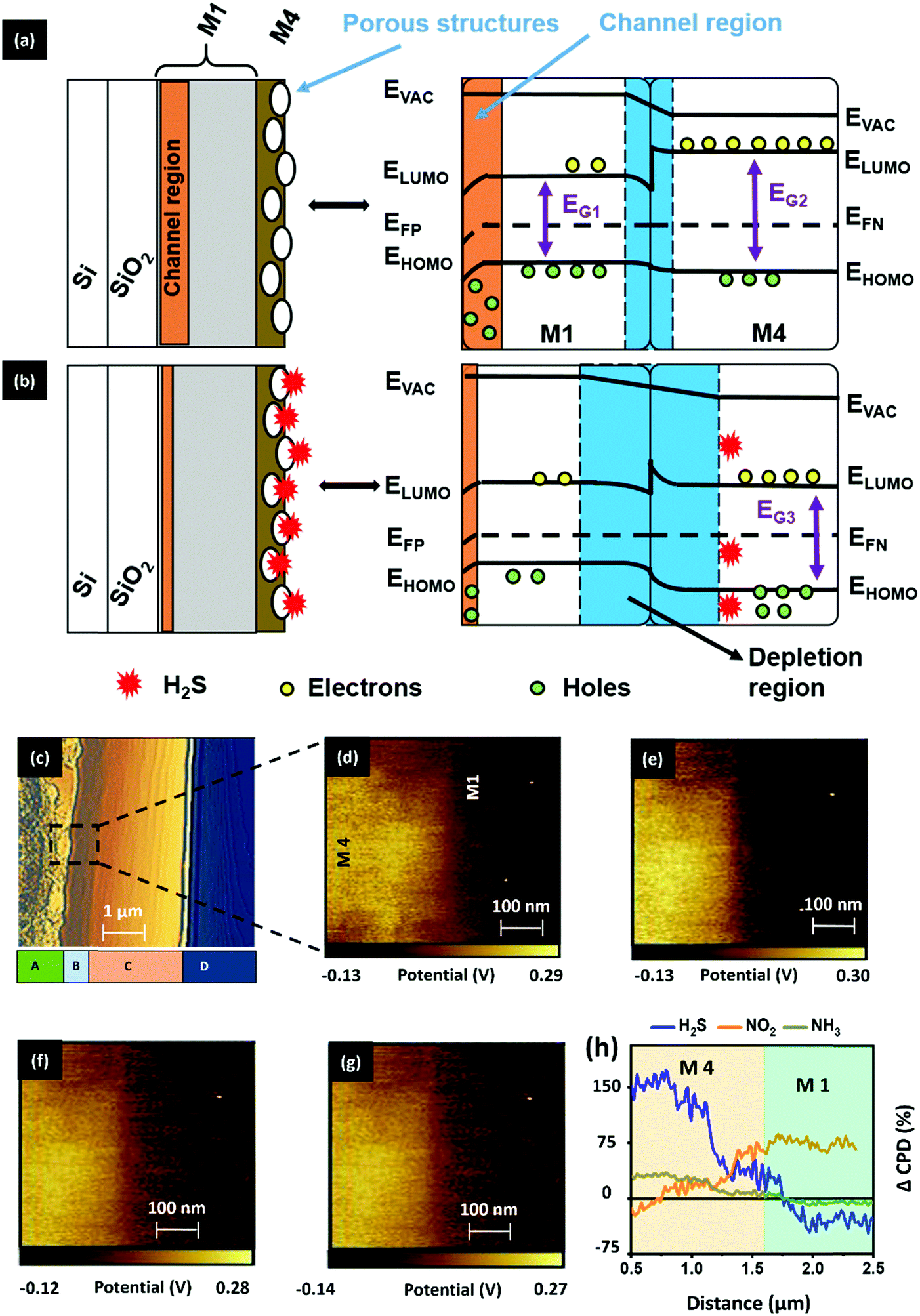 | ||
| Fig. 8 Bandgap and cross-section KPFM characterization of gas-absorbent layers in the presence of gas. Schematic illustration of M1/M4 heterojunction structure energy band diagram changes (a) before and (b) after exposure to H2S gas. (c) Topography phase image of the cross-section D4 device displaying four layers, including the M4 (A), M1 (B), SiO2 (C) and Si (D) materials. The CPD potential map of the M4–M1 interface extracted (d) before gas exposure and in the presence of (e) H2S (1 ppm), (f) NH3 (200 ppm) and (g) NO2 (100 ppm) gas. (h) Trends of Δ CPD (%) probed at the M1–M4 interface in the presence of different tested gases. | ||
As illustrated in Fig. 8b, when the absorbent layer is exposed to gases, the incoming H2S gas gains accessibility to the interface region by passing through the available surface nanopores (< 100 nm) of the M4 material. These gas molecules undergo an acid–base reaction with the M4 material to generate HS− anions (eqn (2)). The ultra-thin smooth M1 film with angstrom- (Å-) sized pores can allow these HS− anions to enter the M1 bulk region. As a result, these anions can trap the holes from the channel region, thereby causing a concurrent positive shift in threshold voltage and a reduction in drain current due to reduced holes (q) in eqn (1). Therefore, we speculate that the cumulative effect of the proposed mechanisms plays a pivotal role in achieving good sensing performance of the D4 OFET sensor.
As discussed before, the observed strong interaction between the base M4 and weak acid H2S gas is a chemisorption process due to an acid–base chemical reaction. For this reason, as observed in the results of the device transient gas response (Fig. 4f), we mildly heated the gas exposed device for a short time at 55 °C, causing the HS− ions to drift back to the M4 material and recombine with H+ ions, reversing eqn (2) to escape as H2S molecules into the N2 inert atmosphere in the gas testing chamber.
| H2S + R3N ⇌ R3NH+ + HS− | (2) |
We probed the surface potential changes that resulted from gas exposure, which occurs at the M1–M4 interface region, using cross-sectional KPFM characterization to confirm the proposed hypothesis. The topography view of the D4 device cross-section is presented in Fig. 8c, differentiating the layers M4, M1, SiO2 and Si as A, B, C and D, respectively. To serve the study requirements, we have selected the M1–M4 interface region and recorded the corresponding CPD map (Fig. 8d).
The extracted map highlights the positive and negative potential distribution, indicating the dominant charge carriers as electrons (M4) and holes (M1), respectively, as discussed before. Followed by this, the sample was exposed to H2S gas and without any further delay, the surface potential map of the exposed region was recorded (Fig. 8e). Similarly, the CPD map was recorded by exposing the sample to NH3 (Fig. 8f) and NO2 (Fig. 8g) gas. While experimenting, the gas-exposed sample was allowed to recover completely for 30 minutes (Fig. S32, ESI†). From the obtained CPD maps, we have traced the CPD values across the region of the exposed samples and calculated the CPD changes (%) by keeping the CPD of the unexposed sample as a reference. The calculated CPD change values were then plotted against the selected interface region (2 μm), as shown in Fig. 8h. As a result, we can confirm that (i) upon interaction of H2S on the surface, M4 will abstract the proton, which will bring about a variation in the electron density, i.e. an increase in electron density on the surface is seen due to the movement of electrons from the bulk. This observation of increased electron density upon proton abstraction was observed using KPFM, supporting the possible mechanism, where upon M4 and H2S interaction, the band gap was lowered slightly, indicating the increased electron density that can be ascribed to the reason stated above. A similar observation, i.e. increased electron density at the surface upon interaction, was also confirmed using theoretical studies, wherein (ii) HS− ions resulting from the reaction between hydrazone and H2S are transferred from M4 to M1. The depletion of electrons in the bulk of M4 after H2S exposure, as can be seen in Fig. 8b, results in an increased barrier potential and increased depletion width at the p–n interface. We hypothesize that the barrier height is increased at the interface because of a quasi-reverse bias effect. In addition, the diffusion of HS− ions from M4 to M1 may deplete the holes in the channel region, essentially reducing the drain current response and increasing the barrier potential. Thus, in both the electrical studies and surface characterization, we observed a good selectivity toward H2S gas. However, the corresponding phenomenon that elucidates the sensing behavior remains different.
Conclusion
In summary, we have designed a novel PDVT-10 (polymer)/tris(keto-hydrazone) (monomer) organic heterostructure-based OFET device, fabricated using an industry-ready CMOS-compatible microfabrication process technique, and explored the detection of different toxic gases operating under room-temperature conditions. Using the microfabrication approach, we developed OFET devices that display repeatable electrical characteristics with minimum variations in the transistor performance. Thus, we successfully configured OFET sensors with good reproducible sensing performance under room temperature operating conditions. When compared to pristine OFETs, the PDVT-10/tris(keto-hydrazone)-based device has shown a 64-fold increase in sensitivity toward H2S gas, along with excellent selectivity, the lowest limit of detection (1 ppb), excellent repeatability and fast reaction/recuperation behavior. The benchmark attributes of the reported organic heterostructure promise room-temperature sensing performance, stability against bias stress (10 hours) and relative humidity (5% to 90% RH) and a 150 day shelf-life with no special device encapsulation. The unprecedented sensing performance of our organic heterostructure sensor toward H2S gas is due to its high surface porous structures, specific acid–base reaction with H2S gas, heterojunctions at the interface of PDVT-10/tris(keto-hydrazone) layers and acidic nature of PDVT-10, with good charge transport properties. We foresee that some of the customizable features of our organic heterostructure OFET sensor, such as optimizing the functional groups of DPP-based organic semiconductors, tuning the heterojunction properties and tuning the chemical nature of hydrazone host compounds, have the potential to attract researchers to our sensor design for different sensing applications.Conflicts of interest
There are no conflicts to declare.Acknowledgements
We acknowledge the financial support of King Abdullah University of Science and Technology (KAUST), Saudi Arabia. SGS and KNS acknowledge the Center Collaborative Fund of the Advanced Membranes and Porous Materials Center at KAUST. CVY sincerely expresses his gratitude to SERB, Department of Science and Technology, Government of India for providing financial support under a research project no. EMR/2017/000153.References
- B. Yuan, T. K. Egner, V. Venditti and L. Cademartiri, Nat. Commun., 2018, 9, 1–7 CrossRef.
- Z. Sun, H. Yuan, Z. Liu, B. Han and X. Zhang, Adv. Mater., 2005, 17, 2993–2997 CrossRef CAS.
- X. Wei, L. Duan, L. Bai, M. Tian, W. Li and B. Zhang, Intensive Care Med., 2012, 38, 1877–1885 CrossRef CAS.
- W. Liang, J. Chen, L. Li, M. Li, X. Wei, B. Tan, Y. Shang, G. Fan, W. Wang and W. Liu, ACS Appl. Mater. Interfaces, 2019, 11, 14619–14629 CrossRef CAS.
- P. M. Bhatt, Y. Belmabkhout, A. H. Assen, Ł. J. Weseliński, H. Jiang, A. Cadiau, D.-X. Xue and M. Eddaoudi, Chem. Eng. J., 2017, 324, 392–396 CrossRef CAS.
- S. Komiyama, O. Astafiev, V. Antonov, T. Kutsuwa and H. Hirai, Nature, 2000, 403, 405–407 CrossRef CAS.
- S. Roy, N. F. Mohd-Naim, M. Safavieh and M. U. Ahmed, ACS Sens., 2017, 2, 1713–1720 CrossRef CAS.
- M. Paknahad, C. Mcintosh and M. Hoorfar, Sci. Rep., 2019, 9, 1–11 CrossRef CAS.
- E. N. Balko, Multi-channel pellistor type emission sensor, US Pat., 6009742, 2000 Search PubMed.
- D. T. McQuade, A. E. Pullen and T. M. Swager, Chem. Rev., 2000, 100, 2537–2574 CrossRef CAS.
- D. T. McQuade, A. E. Pullen and T. M. Swager, Chem. Rev., 2000, 100, 2537–2574 CrossRef CAS.
- J. Zhang, Z. Qin, D. Zeng and C. Xie, Phys. Chem. Chem. Phys., 2017, 19, 6313–6329 RSC.
- T. Nguyen, T. Dinh, A. R. M. Foisal, H.-P. Phan, T.-K. Nguyen, N.-T. Nguyen and D. V. Dao, Nat. Commun., 2019, 10, 1–8 CrossRef.
- B. Wang, A. Thukral, Z. Xie, L. Liu, X. Zhang, W. Huang, X. Yu, C. Yu, T. J. Marks and A. Facchetti, Nat. Commun., 2020, 11, 1–11 Search PubMed.
- S. Yuvaraja, A. Nawaz, Q. Liu, D. Dubal, S. G. Surya, K. N. Salama and P. Sonar, Chem. Soc. Rev., 2020, 49, 3423–3460 RSC.
- S.-F. Yang, X. Zhang, P.-L. Chen, Z.-T. Liu, J.-W. Tian, G.-X. Zhang and D.-Q. Zhang, Adv. Electron. Mater., 2017, 3, 1700120 CrossRef.
- B. Peng, S. Huang, Z. Zhou and P. K. L. Chan, Adv. Funct. Mater., 2017, 27, 1700999 CrossRef.
- F. Zhang, G. Qu, E. Mohammadi, J. Mei and Y. Diao, Adv. Funct. Mater., 2017, 27, 1701117 CrossRef.
- S. Hou, J. Yu, X. Zhuang, D. Li, Y. Liu, Z. Gao, T. Sun, F. Wang and X. Yu, ACS Appl. Mater. Interfaces, 2019, 11, 44521–44527 CrossRef CAS.
- H. Li, W. Shi, J. Song, H. J. Jang, J. Dailey, J. Yu and H. E. Katz, Chem. Rev., 2019, 119, 3–35 CrossRef CAS.
- C.-F. Lu, C.-W. Shih, C.-A. Chen, A. Chin and W.-F. Su, Adv. Funct. Mater., 2018, 28, 1803145 CrossRef.
- Q. Liu, S. E. Bottle and P. Sonar, Adv. Mater., 2020, 32, e1903882 CrossRef.
- A. A. Trul, V. P. Chekusova, M. S. Polinskaya, A. N. Kiselev, E. V. Agina and S. A. Ponomarenko, Sens. Actuators, B, 2020, 128609 CrossRef CAS.
- H. Fan, S. Han, Z. Song, J. Yu and H. E. Katz, Org. Electron., 2019, 67, 247–252 CrossRef CAS.
- T. Mukhopadhyaya, J. S. Wagner, H. Fan and H. E. Katz, ACS Appl. Mater. Interfaces, 2020, 12, 21974–21984 CrossRef.
- G. Lu, K. Wang, X. Kong, H. Pan, J. Zhang, Y. Chen and J. Jiang, ChemElectroChem, 2018, 5, 605–609 CrossRef CAS.
- H. Fan, H. Li, J. Han, N. McKeever, J. Yu and H. E. Katz, ACS Sens., 2019, 4, 3240–3247 CrossRef CAS.
- S. Han, Z. Yang, Z. Li, X. Zhuang, D. Akinwande and J. Yu, ACS Appl. Mater. Interfaces, 2018, 10, 38280–38286 CrossRef CAS.
- S. Yuvaraja, S. G. Surya, V. Chernikova, M. T. Vijjapu, O. Shekhah, P. M. Bhatt, S. Chandra, M. Eddaoudi and K. N. Salama, ACS Appl. Mater. Interfaces, 2020, 12, 18748–18760 CrossRef CAS.
- S. G. Surya, B. N. Ashwath, S. Mishra, A. Karthik, A. Sastry, B. Prasad, D. Rangappa and V. R. Rao, Sens. Actuators, B, 2016, 235, 378–385 CrossRef CAS.
- K. Tang, Z. Song, Q. Tang, H. Tian, Y. Tong and Y. Liu, IEEE Electron Device Lett., 2017, 39, 119–122 Search PubMed.
- Y. Bai and Q. Bai, Subsea engineering handbook, Gulf Professional Publishing, 2018 Search PubMed.
- M. S. Shah, M. Tsapatsis and J. I. Siepmann, Chem. Rev., 2017, 117, 9755–9803 CrossRef CAS.
- A. K. Saha, S. S. Bandyopadhyay, P. Saju and A. K. Biswas, Ind. Eng. Chem. Res., 1993, 32, 3051–3055 CrossRef CAS.
- C. N. Okonkwo, C. Okolie, A. Sujan, G. Zhu and C. W. Jones, Energy Fuels, 2018, 32, 6926–6933 CrossRef CAS.
- X. Su and I. Aprahamian, Chem. Soc. Rev., 2014, 43, 1963–1981 RSC.
- H. Y. Lee, X. Song, H. Park, M.-H. Baik and D. Lee, J. Am. Chem. Soc., 2010, 132, 12133–12144 CrossRef CAS.
- A. S. Sizov, A. A. Trul, V. Chekusova, O. V. Borshchev, A. A. Vasiliev, E. V. Agina and S. A. Ponomarenko, ACS Appl. Mater. Interfaces, 2018, 10, 43831–43841 CrossRef CAS.
- B. Nketia-Yawson and Y.-Y. Noh, Macromol. Res., 2017, 25, 489–495 CrossRef CAS.
- X. Zhuang, S. Han, B. Huai, W. Shi and Y. Junsheng, Sens. Actuators, B, 2019, 279, 238–244 CrossRef CAS.
- H. Li, J. Dailey, T. Kale, K. Besar, K. Koehler and H. E. Katz, ACS Appl. Mater. Interfaces, 2017, 9, 20501–20507 CrossRef CAS.
- Y. Yang, Z. Liu, L. Chen, J. Yao, G. Lin, X. Zhang, G. Zhang and D. Zhang, Chem. Mater., 2019, 31, 1800–1807 CrossRef CAS.
- S. Perlman and D. Feucht, Solid-State Electron., 1964, 7, 911–923 CrossRef.
- Q. Ou, Y. Zhang, Z. Wang, J. A. Yuwono, R. Wang, Z. Dai, W. Li, C. Zheng, Z. Q. Xu and X. Qi, Adv. Mater., 2018, 30, 1705792 CrossRef.
- B. M. Kayes, H. A. Atwater and N. S. Lewis, J. Appl. Phys., 2005, 97, 114302 CrossRef.
- F. Wu, Q. Li, P. Wang, H. Xia, Z. Wang, Y. Wang, M. Luo, L. Chen, F. Chen and J. Miao, Nat. Commun., 2019, 10, 1–8 CrossRef.
- O. Ostroverkhova, Chem. Rev., 2016, 116, 13279–13412 CrossRef CAS.
- H. Ma, S. Chai, D. Chen and J.-D. Huang, IUCrJ, 2017, 4, 695–699 CrossRef CAS.
- B. Souharce, C. J. Kudla, M. Forster, J. Steiger, R. Anselmann, H. Thiem and U. Scherf, Macromol. Rapid Commun., 2009, 30, 1258–1262 CrossRef CAS.
Footnotes |
| † Electronic supplementary information (ESI) available. See DOI: 10.1039/d0mh01420f |
| ‡ Saravanan Yuvaraja and Veerabhadraswamy Nagarajappa Bhyranalyar have contributed equally. |
| This journal is © The Royal Society of Chemistry 2021 |