
 Open Access Article
 This Open Access Article is licensed under a Creative Commons Attribution-Non Commercial 3.0 Unported Licence
CdSe:In Mid-infrared transparent conductive films prospering uncooled PbSe/CdSe heterojunction photovoltaic detectors
Jijun
Qiu
 *ab,
Yun
Liu
a,
Zhihua
Cai
b,
Quang
Phan
b and
Zhisheng
Shi
*b
*ab,
Yun
Liu
a,
Zhihua
Cai
b,
Quang
Phan
b and
Zhisheng
Shi
*b
aSchool of Microelectronics, Dalian University of Technology, Dalian, 116024, P. R. China. E-mail: jjqiu@dlut.edu.cn
bSchool of Electrical and Computer Engineering, University of Oklahoma, Norman, Oklahoma 73019, USA. E-mail: shi@ou.edu
First published on 24th November 2021
Abstract
Infrared transparent and conductive coatings (ITCCs) are in significant demand in infrared imaging applications. The combination of high optical transparency in the infrared range (1–12 μm) and high electrical conductivity, however, sets stringent requirements on ITCC materials. A high carrier concentration (> 1020 cm−3) employed for high conductivity commonly results in a dramatic drop in the transparency and a distinguishable cutoff blueshift (<2 μm) due to the plasmon effect, which is unable to meet the requirements of infrared optoelectronic devices. To overcome this technical issue, herein, we demonstrate indium-doped cadmium selenide (CdSe:In) ITCC electrodes with high transparency in the infrared range and excellent conductive properties. After optimizing the In/CdSe beam flux ratio and substrate temperature, a champion sheet resistance of 22 Ω per sq was achieved on a BaF2 substrate with an electron concentration of 7.6 × 1018 cm−3 and a mobility of 307 cm2 V−1 s−1. The average transmittance is 75% in the 1.0–6.0 μm middle-wavelength infrared (MWIR) range, and more than 50% in the 8–10 μm long-wavelength infrared range (LWIR). By using CdSe:In as an ITCC electrode, we demonstrated an uncooled Au/PbSe/CdSe/CdSe:In/quartz heterojunction photovoltaic detector array. An uncooled PbSe/CdSe PV detector of 50 × 50 μm exhibits an MWIR spectral photo response with a cutoff wavelength of 4.2 μm at room temperature. Under zero-bias photovoltaic mode, the peak responsivity and specific detectivity at room temperature are 0.075 A W−1 and 1.02 × 109 cm Hz1/2 W−1, respectively. Therefore, a CdSe:In ITCCs and PbSe/CdSe heterojunction PV detector provides a technical solution for the manufacturing of low-cost megapixel uncooled lead salt FPA imagers.
1. Introduction
Infrared detectors are widely used in imaging applications, including military signature analysis, space science, environmental monitoring, medical diagnosis, law enforcement/security, and industrial equipment diagnosis.1–4 Most current development efforts in infrared detectors are concentrating on reducing the size, weight, power (SWaP) and cost while keeping high resolution, high sensitivity and high speed.5 A significant way to reduce the SWaP and cost is to develop high operating temperature (HOT) infrared detector technologies (>150 K), where traditional cooling systems, such as liquid-nitrogen Dewar or Stirling coolers, could be removed or replaced by thermo-electric coolers.6 Two major technologies have been developed for this goal: thermal detectors7–9 and high-temperature photodetectors. Thermal detectors, including microbolometers,10 and pyroelectric,11 thermoelectric,12 thermoresistive13 and thermomechanical sensors,14 which rely on IR absorption induced temperature change, have achieved relatively high sensitivity at room temperature or even above room temperature. However, these uncooled IR thermal detectors generally demonstrate a slow response, and seem to be unsuitable for future IR imaging systems, which are moving toward faster frame rates and multispectral operation.1–6 Simultaneously, more efforts have been spent on developing high HOT infrared photodetectors based on narrow bandgap semiconductors, most notably mercury–cadmium–telluride (MCT),15–19 In As/GaSb type-II superlattices (T2SLs),20,21 and inter sub-band based quantum dot infrared photodetectors (QDIPs).22–25 However, there is an inherent and reasonable contradiction between high sensitivity and high operating temperature due to the recombination processes of photoexcited carriers, in particular, by Auger recombination. Additionally, although state-of-the-art HOT photodetectors based on epitaxial materials have already demonstrated near-room-temperature operation, the cost is still plagued by nonuniform growth, expensive substrates, slow output rate and the high cost of equipment, especially molecular beam epitaxy (MBE). Recently, 2D van der Waals infrared photodetectors have been proposed based on the development of nanotechnology, including two-dimensional (2D) layered black arsenic phosphorus (b-AsP)26 and graphene.27–30 Unfortunately, 2D van der Waals infrared devices suffer from several major challenges, such as sophisticated device processing and difficult industrialization, that limit their wide applications.Suppressing high Auger recombination is key to improving the sensitivity of HOT photodetectors made of narrow band gap materials. Based on our previous work31–33 on room-temperature infrared detectors, three approaches have been considered to suppress Auger and Shockley–Read–Hall (SRH) recombination: (1) choosing narrow band gap materials with a lower Auger coefficient as infrared radiation absorbers; (2) improving the crystal quality of the narrow band gap materials, and (3) building a heterogenous structure by combining narrow band gap materials with wide band gap materials where Auger recombination plays a negligible role. It is well known that the Auger coefficient in IV–VI PbSe is over an order of magnitude lower than those in III–V (InAs, InAsxSb1−x) or II–VI (CdxHg1−xTe) semiconductors with the same band gap.34 At the same time, the band gap of PbSe could be precisely tailored from 0.3 to 0.1 eV by forming a Pb1−xSnxSe (0 ≤ x ≤ 0.23) solid solution,35,36 which broadens the detection range to long-wavelength IR (8–14 μm), making PbSe a highly attractive material for ultra-broadband photodetection and energy conversion. Additionally, high-quality (100) oriented poly-crystalline PbSe films could be synthesized by various low-cost methods, including vapor physical deposition (VPD)37 and chemical bath deposition (CBD).38 These oriented PbSe films are assembled from low-defect mono-crystalline PbSe cuboids due to their distinctive nature of self-crystallization, while the intrinsic defects located in the cuboid boundaries could be effectively eliminated by interface passivation, resulting in an improvement in material quality.39 Furthermore, reports show that PbSe epitaxial films could possibly form a heterojunction with other wide band gap semiconductors, such as PbSeO3,40 CdS31 or CdTe,41 where the reduced Auger recombination results in a measurable spectral photoresponse up to 5 × 108 cm Hz1/2 W−1 at room temperature. The above-mentioned merits of PbSe make it a promising candidate for low-cost HOT photodetectors with high sensitivity.
However, the lack of a high infrared transparent conducting coating (ITCC) hampers the further development of highly integrated infrared polycrystalline PbSe heterojunction photodetectors. Compared with traditional metallic grid electrodes, continuous ITCCs have been more desirable for MIR photodetectors due to (1) no distortion being caused; (2) enhanced pixel-level sensing and processing capabilities (smart pixels), and (3) reduced communication traffic loads between the image sensors and the subsequent image processing electronics.42,43 However, it is still a big challenge to achieve high infrared transparency and high conductivity simultaneously for state-of-the art ITCCs. The most common transparent conductive materials system is transparent conductive oxide (TCO), involving (In2O3:Sn, ITO), fluorine-doped tin oxide (Sn2O3:F, FTO), or aluminium-doped zinc oxide (ZnO:Al, AZO). The most remarkable characteristics of TCO films are their high transmittance (>80%) in the visible–near infrared range and low resistivity (10−3 Ω per cm), good friction resistance, chemical stability, strong adhesion and impact resistance.44 However, the transmittance of TCO electrodes decreases sharply when the wavelength is greater than 2 μm, limiting their applications in middle-wavelength infrared (MWIR) and far-wavelength infrared (LWIR) optoelectronic devices. Although dysprosium-doped cadmium oxide (CdO:Dy) grown by oxide-molecular beam epitaxy (OMBE) has recently been developed and exhibits high transparency as well as good electrical properties, its applications in MIR photodetectors are limited by the complicated, expensive fabrication process, unstable chemical properties and incompatibility with Si-processing.45,46 As a promising p-type TCO film, CuAlO2 has attracted wide attention due to its high transmittance in the MIR range; however, its low mobility of <3 cm2 V−1 S−1 and high synthesis temperature (>900 °C) are not adequate for infrared detection devices and imaging systems.47 CNT film exhibits a significant transparency of over 80% over the whole IR range (1–22 μm); however, it has a relatively high resistivity of around 200 Ω per sq.48 2 nm ultrathin metal film has a mean transmittance above 80% in the IR range of 2.5–25 μm, but a resistivity of around 1000 Ω per sq.49 Graphene and conductive polymers offer ideal chemical and mechanical properties, but both their transparency and conductivity are inferior to those of most of the aforementioned materials.48–54 In addition, doped semiconductor wafers or epitaxial layers (doped Si, Ge, GaAs, InP) do not cover the entire spectral range, resulting in limited utility.55
In this paper, we demonstrate indium-doped cadmium selenide (CdSe:In) as a novel ITCC candidate in the 1–12 μm infrared range. Under optimized conditions, a CdSe:In ITCC is able to achieve a suitable doping concentration of about 7.6 × 1018 cm−3, a high mobility of 307 cm2 V−1 s−1 and a resultant very low sheet resistance of 22 Ω per sq. Meanwhile, it exhibits 75–80% transmission in the visible–MWIR region of 0.6–6 μm and about 60% in the LWIR region of 6–10 μm. The combination of excellent optical–electrical properties, suitable chemical stability, and capability with Si-processing makes CdSe:In a promising new MWIR ITCC material. This was further confirmed by a high-performance room-temperature MWIR hybrid PV detector based on a polycrystalline PbSe/CdSe heterojunction, where CdSe:In was firstly used as an ITCC electrode to extract separated charge carriers from the n-type CdSe, as shown in the structural scheme in Fig. 1(a). Combined with a PbSe/CdSe heterojunction, a room-temperature-specific detectivity greater than 1.0 × 109 cm Hz1/2 W−1 was obtained in the 1–5 μm range. Our PbSe/CdSe heterojunction PV detectors not only exemplify CdSe:In as a promising candidate for MWIR ITCC, but also pave the way for high-performance, low-cost megapixel uncooled lead salt FPA imagers.
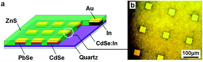 | ||
| Fig. 1 Structural design for an Au/PbSe/CdSe/CdSe:In/quartz polycrystalline heterojunction photovoltaic detector. (a) Schematic drawing of the detector, and (b) nomarski photograph of 50 × 50 μm PbSe/CdSe mesa arrays. | ||
2. Experimental
All material sources used in the experiment were of high purity, more than 99.999%, and the material growth was carried out in a home-made vacuum thermal evaporation chamber with four effusion cells.2.1 Materials growth
CdSe:In ITCC films were synthesized on various infrared transparent substrates by co-evaporation of CdSe, indium and selenium. The indium doping concentration was tailored by controlling the In/CdSe beam flux ratio in the range from 0.15% to 1.5%. For that, the source temperatures of CdSe and Se cell were fixed at 870 and 300 °C while the temperature of the indium cell changed from 550 to 620 °C. Simultaneously, the substrate growth temperature was tailored from 220 to 400 °C to optimize the optical and electric properties. After the growth of the CdSe:In ITCC, the substrates were cooled to room temperature at a rate of 2 °C min−1 in the chamber. Subsequently, intrinsic 1.5 μm CdSe film was deposited over the CdSe:In at room temperature for 90 min. After finishing the intrinsic CdSe growth, the substrate temperature was increased again to 400 °C at a rate of 5 °C min−1. Then, the temperature of the PbSe effusion cell was raised and maintained at 810 °C for 2 h to deposit PbSe film (2 μm) over the CdSe/CdSe:In/quartz substrates. An additional Se source (330 °C) was used to ensure the p-type and the material quality due to the high Se vapor pressure during growth.2.2 Heterojunction photovoltaic detector fabrication
A photoresist (AZ5241E) layer was coated onto PbSe/CdSe/CdSe:In/quartz films by spin-coating at 2500 rpm for 60 s followed by a soft bake at 90 °C for 90 s. Then, quadrate photoresist arrays of 100 × 100 μm were patterned using MJB3 mask aligner UV lithography (275 W) with an exposure time of 10 s, followed by a development time of 45 s. Subsequently, the PbSe/CdSe arrays on CdSe:In ITCC were patterned by wet-chemical etching for 50 s. The etchant consists of equal parts of 80% H3PO4, 29% HCl, and H2O. Then a 200 nm thickness of indium film, as a common electrode, was deposited over the CdSe:In at one corner by using shadow-mask thermal evaporation at room temperature, as shown in Fig. 1(a). Next, a 3.5 μm ZnS passivation layer was deposited on the PbSe/CdSe patterns with a photoresist layer (without lift-off) by using a thermal evaporation technique. The deposition was carried out at a 25 °C substrate temperature and lasted for 120 min in 4 × 10⁻⁴ Pa. After acetone lift-off for 120 s, the pixel electrode pattern (50 × 50 μm) was then shaped by a second lithographic process, with spin-coating at 2500 rpm for 60 s, a soft bake at 95 °C for 90 s, exposure for 4 s, a hard bake at 120 °C for 90 s, UV exposure for 50 s and development for 60 s. Then 100 nm thick Au electrodes were deposited by employing thermal evaporation at room temperature for 20 min at 2 × 10⁻⁴ Pa. Subsequently a set of photodiodes with Au/PbSe/CdSe/CdSe:In/quartz structures were fabricated after lift-off with acetone for 300 s. Finally, the devices were post-annealed at 230 °C for 0.5 h in an argon atmosphere.2.3 Structure and morphology, optoelectronic and device characterizations
The morphologies of the synthesized thin films were characterized with a Zeiss Neon-40 EsB high-resolution field-emission scanning electron microscope (FESEM). Hall effect measurement was conducted in van der Pauw four-point probe configuration, using fresh indium contacts, in an automated EGK HEM-2000, with a magnetic induction of 0.37 T. The transmission spectra of the samples were measured by the FTIR system with an Si detector for 350–1500 nm and a DLATGS detector for 1–10 μm. The dark current density–voltage (J–V) behaviour was measured at room temperature by applying a bias from −1 to 1 V (Keithley 2400 source meter).The detector performance at room temperature was evaluated by a home-made detectivity measurement system, consisting of an IR-508/301 blackbody (Infrared System Development), an IR-762 modulator (Infrared System Development), an SR830 Lock-in Amplifier (Stanford Research System) and an ST-500 probe station (Janis Research). In this measurement system, a calibrated 500 K blackbody supplied the standard infrared radiation source. The mechanical energy modulator of 200 Hz was integrated to become a frequency-modulated heat source. Without connecting to any preamplifier, signal and noise currents from the devices were directly collected by the Lock-in Amplifier in zero-bias photovoltaic mode.
The responsivity R and specific detectivity D* were obtained as described in our previous work by using the definitions shown below:
3. Results and discussion
To verify its versatility, CdSe:In was deposited on various MWIR transparent substrates, including BaF2, quartz and silicon wafers and glass slides. The champion electrical properties on various substrates were obtained after optimizing the In/CdSe beam flux ratio and the substrate temperature. Fig. 2(a) shows the carrier density, Hall mobility and conductivity of the CdSe:In films as a function of the beam flux ratio of In/CdSe fabricated at 270 and 350 °C substrate temperatures. Regardless of the substrate temperature, the optimized In/CdSe beam flux ratio is in the range of 0.3–0.6%, depending on the substrates. In this flux ratio range, the higher growth temperature contributes to higher concentration and mobility, then to higher conductivity in this flux range. For example, the CdSe:In grown on the BaF2 substrate approaches a conductivity of 380 1 Ω per cm at 0.3% beam flux ratio at 350 °C, whereas CdSe:In grown on Si and glass goes up to highest conductivities of 252 and 223 1 Ω per cm at 0.6%. Based on the XRD pattern (shown in Fig. 4(i)), the highest conductivity for the BaF2 substrate is attributed to its (002) oriented growth direction. In addition, CdSe:In ITCCs deposited at 350 °C with a beam flux ratio higher than 0.6% will peel off from all the substrates in the course of cooling down. After fixing the beam flux ratio at 0.6%, wider growth temperatures from 200 to 400 °C were studied, as shown in Fig. 2(b). Regardless of the substrate, the conductivity increases with an increase in the temperature, and reaches a maximum at 350 °C, then decreases with a further increase in temperature. Notice that when the In/CdSe flux ratio was fixed at 0.6%, no CdSe:In films could survive on the Si and glass substrates as the growth temperatures are lower than 350 °C and 270 °C, respectively. This may be caused by the difference in the thermal expansion coefficients between CdSe:In and the substrates. The choice order of substrates for the CdSe:In ITCCs is BaF2 > glass > Si. The electrical properties of the champion CdSe:In on various substrates are summarized in Table 1.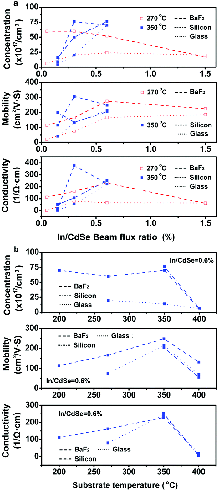 | ||
| Fig. 2 The dependency of technological parameters on the electrical properties of CdSe:In ITCCs. (a) In/CdSe beam flux ratio and (b) substrate temperature dependence of carrier concentration, Hall mobility and conductivity of CdSe:In ITCCs. | ||
| Subsstrate | Concentration cm3 | Mobility cm2 V−1 S−1 | Conductivity Ω−1 cm−1 | Thickness μm | Sheet resistance |
|---|---|---|---|---|---|
| BaF2 | 7.6 × 10¹⁸ | 307 | 376 | 1.2 | 22 |
| Quartz | 7.0 × 10¹⁸ | 214 | 223 | 1.8 | 25 |
| Silicon | 7.6 × 10¹⁸ | 204 | 252 | 1.0 | 40 |
The transmittances of CdSe:In ITCCs deposited on various substrates are shown in Fig. 3. As can be seen from Fig. 3(a), the transmission of CdSe:In ITCC on BaF2 with 22 Ω per sq remains constant at around 75% throughout the 700 nm to 6 μm range, and >50% extending to 10 μm. The simulated transmittance spectrum (black) in the infrared range, which was extracted from its electrical parameters, matches well with the experimental transmittance (red). The transmission of CdSe:In ITCC on Si with 40 Ω per sq, which is achieved under an electron density of 7.6 × 1018 cm−3 and mobility of 204 cm2 V−1 s−1, is 57% in the MWIR (3.0–5.0 μm) region, and approaches 40% in the long-infrared (8–10 μm) region. The 57% transmittance of CdSe:In is approximately equal to that of a DSP Si wafer in the MWIR range, indicating a simultaneous coupling of high infrared transparency and high conductivity. The simulated transmittance agrees well with the experimental results, indicating a high simulation accuracy. Therefore, a simulated transmittance of CdSe:In grown on a glass substrate, which is opaque in the near–mid infrared range, is convincing, as shown in Fig. 3(a). This shows a high transmittance of about 60% or more in the MWIR range.
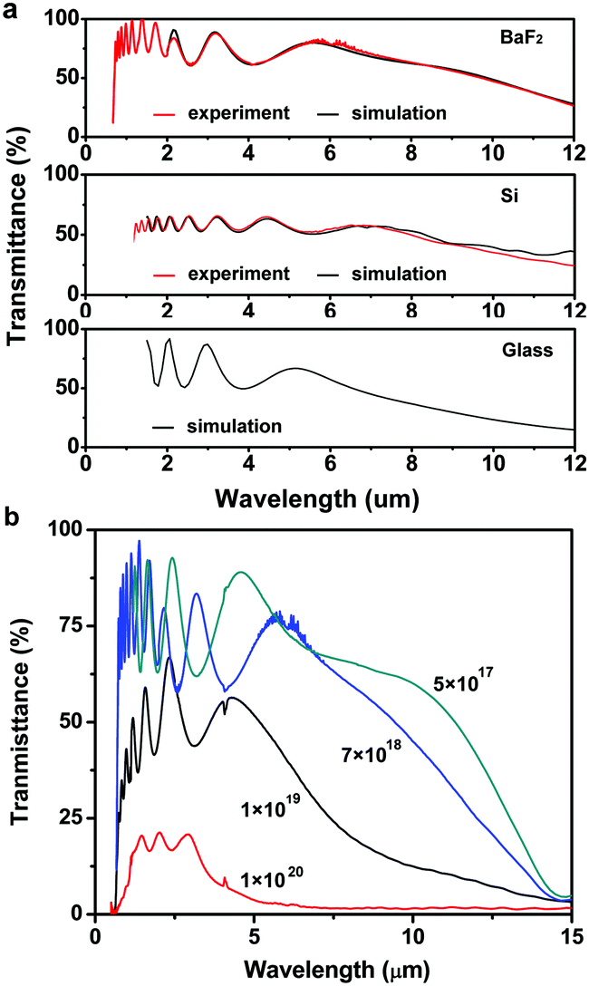 | ||
| Fig. 3 The transmittance spectra of CdSe:In ITCCs obtained from various technological parameters. (a) The experimental and simulated transmittances of the champion CdSe:In ITCCs on various substrates, and (b) the experimental transmittances of the CdSe:In ITCCs with various carrier concentrations. | ||
It is well known that a higher carrier concentration can help to increase the conductivity of TCO films. For CdSe:In ITCCs, a typical carrier concentration is 7.8 × 1018 cm−3. A concentration lower than 1018 cm−3 results in a distinguished degradation in conductivity of 10−1 Ω−1 cm−1, while ITCCs with a high concentration of more than 1019 cm−3 show a lower transmittance in the infrared region and a remarkable blueshift of the cutoff wavelength with an increase in the carrier concentration, as shown in Fig. 3(b). The decrease in transmittance and blueshift of the cutoff wavelength is attributed to the electron–electron scattering and electron–impurity scattering,54,55 which could be confirmed by the decline in mobility by two orders of magnitude. Therefore, a high mobility of 200–300 cm2 V−1 s−1 and a moderate carrier concentrate concentration of 7 × 1018 cm−3 are critical for an infrared-transparent conductive coating.
Fig. 4 shows the morphologies and crystal structures of CdSe:In films grown on the various substrates. On a BaF2 substrate, a textured morphology could be observed, which is made up of crystalline flakes of 1 μm in length and 200 nm in width. Its XRD pattern in Fig. 4(i) shows one peak at 25.34°, corresponding to the (002) face of wurtzite CdSe, indicating a (002) growth orientation on the BaF2(222) plane. CdSe:In films on an Si wafer are constructed from crystalline columns with a (110) growth orientation, as shown in Fig. 4(d and h). The average size of the crystalline columns is about 250–300 nm, orienting in the (110) direction. The CdSe:In growth on a glass substrate shows a small particle size and a stronger (110) growth orientation due to the high (110)/(103) ratio, as shown in Fig. 4(e and g).
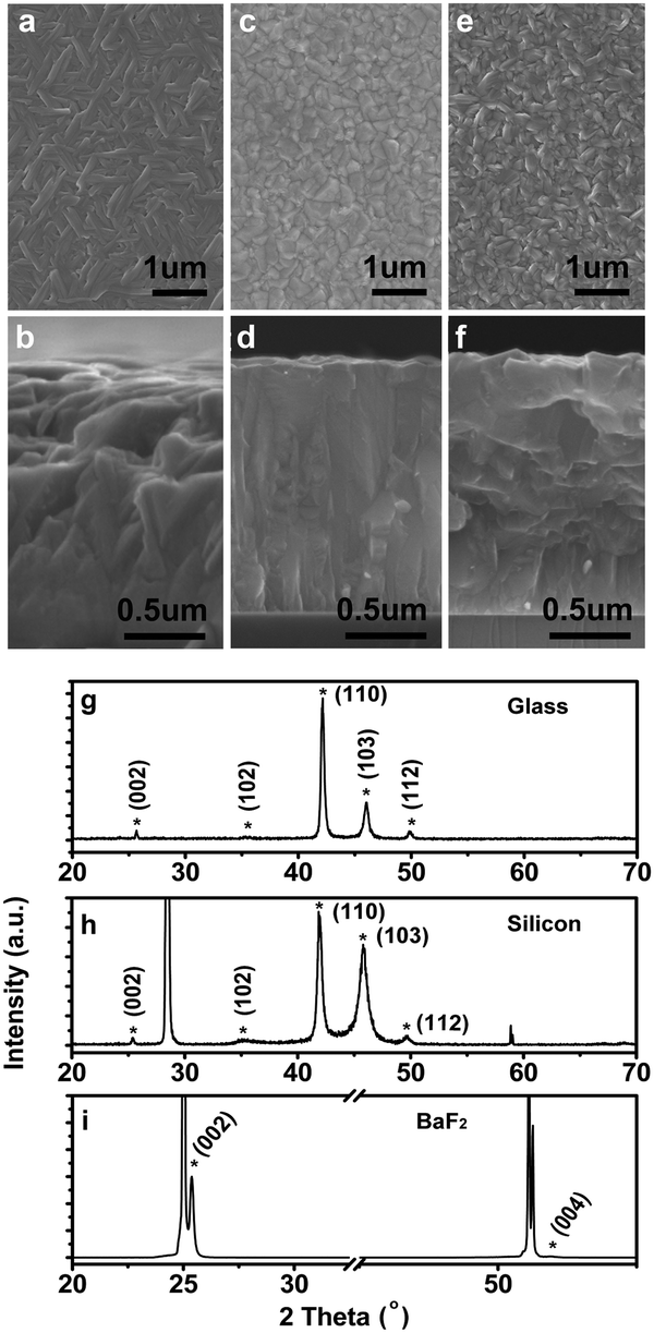 | ||
| Fig. 4 The typical morphologies and XRD patterns of champion ITCCs grown on various substrates. (a, c) and (e) are top-views, (b, d) and (f) are side-views of FESEM images on BaF2, Si and glass substrates, respectively. (g, h) and (i) are XRD patterns of ITCCs grown on glass, Si and BaF2 substrates. | ||
The investigated photosensitive PbSe/CdSe heterostructures consist of 2.0 μm p-type PbSe films, 1.5 μm n-type intrinsic CdSe films and 1.2 μm CdSe:In ITCCs. Prior to the formation of an ohmic contact to the n-type CdSe:In ITCC, the top-most layers of p-PbSe and n-type CdSe were removed by etching in equal parts of 80% H3PO4, 29% HCI, and H2O to form mesa-type structures, as shown in Fig. 1(b). Then, this contact was completed by 200 nm of indium deposited onto the ITCC. Subsequently, a ZnS insulator layer was filled between the mesa as a passivation layer. Finally, the ohmic contacts to p-PbSe were formed by the deposition of Au by thermal evaporation.
Fig. 5(a) shows the XRD diffusion patterns for PbSe/CdSe/CdSe:In/quartz devices. The XRD diffraction pattern (black) of CdSe:In grown on the quartz substrate does not indicate an orientation growth due to the similar intensities of the (002) and (110) peaks. This is confirmed by the side-view FESEM image of the device shown in Fig. 5(c), where no obvious column crystals were observed. After deposition of intrinsic CdSe, a strong peak at 41.8° (red) in the XRD pattern and the column morphology demonstrate a (110) orientated growth of intrinsic CdSe. Subsequently, highly (200) orientated PbSe with high crystallinity could be obtained over a CdSe/CdSe:In/quartz substrate. This could be proved by the sharp peak at 29.2° in the XRD pattern (blue) and large column crystals of 0.5–1.0 μm size in the FESEM images.
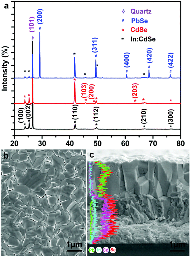 | ||
| Fig. 5 Structural characteristics of the PbSe/CdSe/CdSe:In/quartz device. (a) XRD patterns, (b) top-view and (c) side-view FESEM images. | ||
The EDS shown in Fig. 5(c) indicates an obvious indium diffusion from the CdSe:In electrode to intrinsic CdSe film. At the same time, no indium was detected in the PbSe layer. It should be noted that intrinsic CdSe is critical to obtaining an infrared response. Without intrinsic CdSe, a p–n junction character current–voltage could be obtained; however, no infrared response was observed. Therefore, room temperature was employed to suppress the diffusion of indium to the intrinsic n-type CdSe layer.
The CdSe:In on quartz with 25 Ω per sq retains 70% transmittance in the near and mid-infrared range of 1–4 μm, as shown in Fig. 6(a). The 4.5 μm cutoff is determined by the quartz optical properties. After deposition of intrinsic CdSe, the transmittance in the near-infrared range decreases slightly, and remains at 70% in the mid-infrared range, as shown in Fig. 6(b). The decreased transmittance in the near-infrared range may be attributed to the interface scattering between CdSe:In and CdSe, which transforms from random to orientation growth.
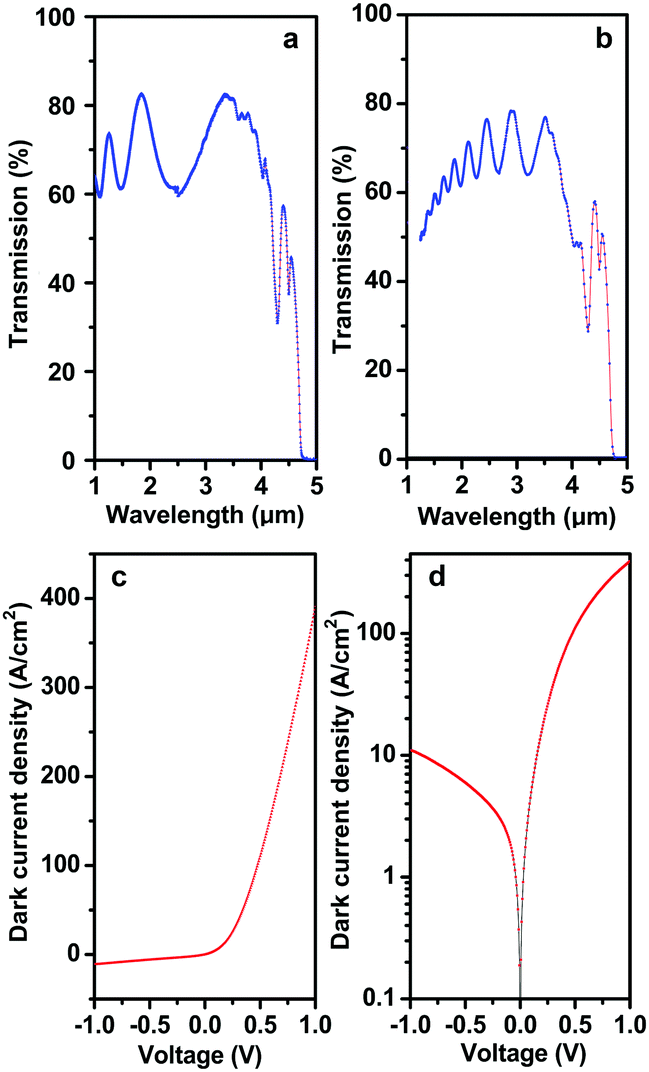 | ||
| Fig. 6 Photo-electrical characteristics of the Au/PbSe/CdSe/CdSe:In/quartz PV detector. The transmittance spectrum of (a) CdSe:In ITCC and (b) CdSe/CdSe:In on quartz substrates. The current density of the device in (c) linear and (d) logarithmic form. | ||
The dark current density–voltage (J–V) of a PbSe/CdSe/CdSe:In/quartz PV detector with 50 × 50 μm pixels was measured, as shown in Fig. 6(c and d). By applying both reverse and forward bias from −1 to 1 V, it is clear that the heterojunction shows diode behaviour according to the rectifying current flow through the junction. The rectifying ratio measured at ±1.0 V is 35.6. The dark current density is 0.27 A cm−2 at −10 mV. The forward J–V characteristic of a p–n junction can be described by the exponential relation J ∝ exp(qV/ηkBT) when exp(qV/ηkBT) ≫ 1, where V is the bias voltage, and η is the ideality factor. Using the data from 0.05 to 0.15 V, η is determined by curve fitting to be 2.0, which indicates that the recombination current may play a major role in this range. It is further confirmed by the fact that the dark current increases with an increase in the reverse-bias voltage. In addition, this also implies that the recombination possibly derives from interface imperfections, resulting in tunnelling or leakage across the junction.
Under 200 Hz chopping frequency modulation, the detector demonstrates an S/N ratio of 21, an Rpeak of 0.075 A W−1, and then a D* peak of 1.02 × 109 cm Hz1/2 W−1 at λ = 3.7 μm at 25 °C in photovoltaic mode. A typical responsivity spectrum measured at room temperature is shown in Fig. 7. A broad peak spanning 2–4.5 μm wavelength is observed from the room-temperature responsivity spectrum, and the peak wavelength is located at 3.7 μm. The small dip around 4.1 μm in the responsivity spectrum is due to CO2 atmospheric absorption.
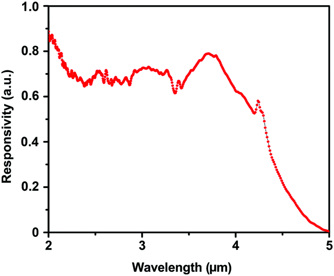 | ||
| Fig. 7 Room-temperature spectral response curve of the Au/PbSe/CdSe/CdSe:In/quartz PV detector. | ||
4. Conclusion
In summary, indium-doped cadmium selenide (CdSe:In) ITCC electrodes with excellent transparent and conductive properties were fabricated by co-evaporation of CdSe, indium and selenium. The optimized substrate temperature is 350 °C, and the In/CdSe beam flux ratio is in the range of 0.3–0.6%, depending on the chosen substrates. The champion sheet resistance of 22 Ω per sq is achieved on a BaF2 substrate with an electron concentration of 7.6 × 1018 cm−3 and a mobility of 307 cm2 V−1 s−1. The average transmittance is 75% in the 1.0–6.0 μm MWIR range, and is more than 50% in the 8–10 μm LWIR. By using CdSe:In as an ITCC electrode, an uncooled PbSe/CdSe heterojunction photovoltaic detector arrays was proposed with a structure of Au/PbSe/CdSe/CdSe:In/quartz. The uncooled PbSe/CdSe PV detector exhibits an MWIR response with a cutoff wavelength of 4.2 mm at room temperature. In zero-bias photovoltaic mode, the peak responsivity and specific detectivity of a 50 × 50 μm PbSe/CdSe PV detector are 0.075 A W−1 and 1.02 × 109 cm Hz1/2 W−1, respectively. Therefore, a CdSe:In ITCC and PbSe/CdSe PV detector provides a technical solution for the manufacture of low-cost megapixel uncooled lead salt FPA imagers.Author contributions
J. Q. conceived the presented idea, carried out the materials growth, performed the characterization, analysed the data and wrote the manuscript with support from Y. L. J. Q. and Z. C carried out the detector fabrication. Q. P. performed the measurement of the detectors and made the simulation of the transmittances. Both J. Q. and Z. S. contributed to the final version of the manuscript. Z. S. supervised the findings of this work.Conflicts of interest
There are no conflicts to declare.Acknowledgements
All conceptual and experimental work were completed at the University of Oklahoma, which was supported by the US DARPA WIRED program through Northrop Grumman, and US army research office (ARO) under contract no. W911NF-18-1-0418. The manuscript was completed at Dalian University of Technology, China.Notes and references
- A. Rogalski, History of infrared detectors, Opto-Electron. Rev., 2012, 20, 279–308 Search PubMed.
- A. Rogalski, Infrared detectors: an overview, Infrared Phys. Technol., 2002, 43, 187–210 CrossRef.
- A. Rogalski, Infrared detectors: status and trends, Prog. Quantum Electron., 2003, 27, 59–210 CrossRef CAS.
- P. Norton, Third-generation sensors for night vision, Opto-Electron. Rev., 2006, 14, 1–10 CAS.
- A. Rogalski, P. Martyniuk and M. Kopytko, Challenges of small-pixel infrared detectors: a review, Rep. Prog. Phys., 2016, 79, 046501 CrossRef CAS PubMed.
- P. Martyniuk and A. Rogalski, HOT infrared photodetectors, Opto-Electron. Rev., 2013, 21, 239–257 CAS.
- G. Hyseni, N. Caka and K. Hyseni, Infrared thermal detectors parameters: semiconductor bolometers versus pyroelectrics, WSEAS Trans. Circuits Syst., 2010, 9, 238–247 Search PubMed.
- F. Niklaus, C. Vieider and H. Jakobsen, MEMS-based uncooled infrared bolometer arrays: a review, in SPIE/COS Photonics Asia, 2007.
- P. L. Richards, Bolometers for infrared and millimeter waves, J. Appl. Phys., 1994, 76, 1–24 CrossRef CAS.
- R. Bhan, R. Saxena, C. Jalwani and S. Lomash, Uncooled Infrared Microbolometer Arrays and their Characterisation Techniques, Def. Sci. J., 2009, 59, 580–589 CrossRef CAS.
- M. D. Aggarwal, A. K. Batra, P. Guggilla, M. E. Edwards, B. G. Penn and J. R. Currie, Pyroelectric Materials for Uncooled Infrared Detectors: Processing, Properties, and Applications, 2010.
- S. B. Riffat and X. Ma, Thermoelectrics: a review of present and potential applications, Appl. Therm. Eng., 2003, 23, 913–935 CrossRef.
- T. Dinh, H.-P. Phan, A. Qamar, P. Woodfield, N.-T. Nguyen and D. V. Dao, Thermoresistive Effect for Advanced Thermal Sensors: Fundamentals, Design Considerations, and Applications, J. Microelectromech. Syst., 2017, 26, 966–986 CAS.
- U. Adiyan, F. Civitci, O. Ferhanoglu, H. Torun and H. Urey, A 35 μm Pitch IR Thermo-Mechanical MEMS Sensor With AC-Coupled Optical Readout, IEEE J. Sel. Top. Quantum Electron., 2015, 21, 87–92 Search PubMed.
- J. Piotrowski, J. Pawluczyk, A. Piotrowski, W. Gawron, M. Romanis and K. Kłos, Uncooled MWIR and LWIR photodetectors in Poland, Opto-Electron. Rev., 2010, 18, 318–327 Search PubMed.
- A. Rogalski, History of HgTe-based photodetectors in Poland, Opto-Electron. Rev., 2010, 18, 284–294 Search PubMed.
- S. U. Eker, M. Kaldirim, E. Sasmaz, A. Tolungüç, B. Asici, A. San, B. Barutcu, S. Ozer, O. Demircioglu and H. C. Erouglu, The status of MCT detector development at ASELSAN, in Infrared Technology and Applications XLIV, ed. G. F. Fulop, C. M. Hanson, P. R. Norton, B. F. Andresen and J. L. Miller, SPIE, Orlando, United States, 2018, p. 32 Search PubMed.
- P. Bensussan, P. Tribolet, G. Destefanis and M. Sirieix, Fifty years of successful MCT research and production in France, Proc. SPIE, 2009, 7298, 72982N CrossRef.
- P. R. Bratt, S. M. Johnson, D. R. Rhiger, T. Tung, M. H. Kalisher, W. A. Radford, G. A. Garwood and C. A. Cockrum, Historical perspectives on HgCdTe material and device development at Raytheon Vision Systems, Orlando, Florida, USA, 2009, vol. 7298, p. 72982U Search PubMed.
- E. A. Plis, InAs/GaSb Type-II Superlattice Detectors, Adv. Electron., 2014, 2014, 1–12 CrossRef.
- A. Rogalski, P. Martyniuk and M. Kopytko, InAs/GaSb type-II superlattice infrared detectors: Future prospect, Appl. Phys. Rev., 2017, 4, 031304 Search PubMed.
- P. Martyniuk and A. Rogalski, Quantum-dot infrared photodetectors: Status and outlook, Prog. Quantum Electron., 2008, 32, 89–120 CrossRef.
- A. D. Stiff-Roberts, Quantum-dot infrared photodetectors: a review, J. Nanophotonics, 2009, 3, 031607 CrossRef.
- H. C. Liu, M. Gao, J. McCaffrey, Z. R. Wasilewski and S. Fafard, Quantum dot infrared photodetectors, Appl. Phys. Lett., 2001, 78, 79–81 CrossRef CAS.
- D. Palaferri, Y. Todorov, A. Bigioli, A. Mottaghizadeh, D. Gacemi, A. Calabrese, A. Vasanelli, L. Li, A. G. Davies, E. H. Linfield, F. Kapsalidis, M. Beck, J. Faist and C. Sirtori, Room-temperature nine-μm-wavelength photodetectors and GHz-frequency heterodyne receivers, Nature, 2018, 556, 85–88 CrossRef CAS PubMed.
- M. Long, A. Gao, P. Wang, H. Xia, C. Ott, C. Pan, Y. Fu, E. Liu, X. Chen, W. Lu, T. Nilges, J. Xu, X. Wang, W. Hu and F. Miao, Room temperature high-detectivity mid-infrared photodetectors based on black arsenic phosphorus, Sci. Adv., 2017, 3, e1700589 CrossRef PubMed.
- B. Y. Zhang, T. Liu, B. Meng, X. Li, G. Liang, X. Hu and Q. J. Wang, Broadband high photoresponse from pure monolayer graphene photodetector, Nat. Commun., 2013, 4, 1811 CrossRef PubMed.
- M. Long, E. Liu, P. Wang, A. Gao, H. Xia, W. Luo, B. Wang, J. Zeng, Y. Fu, K. Xu, W. Zhou, Y. Lv, S. Yao, M. Lu, Y. Chen, Z. Ni, Y. You, X. Zhang, S. Qin, Y. Shi, W. Hu, D. Xing and F. Miao, Broadband Photovoltaic Detectors Based on an Atomically Thin Heterostructure, Nano Lett., 2016, 16, 2254–2259 CrossRef CAS PubMed.
- Y. Chen, Y. Wang, Z. Wang, Y. Gu, Y. Ye, X. Chai, J. Ye, Y. Chen, R. Xie, Y. Zhou, Z. Hu, Q. Li, L. Zhang, F. Wang, P. Wang, J. Miao, J. Wang, X. Chen, W. Lu, P. Zhou and W. Hu, Unipolar barrier photodetectors based on van der Waals heterostructures, Nat. Electron, 2021, 4, 357–363 CrossRef CAS.
- C.-H. Liu, Y.-C. Chang, T. B. Norris and Z. Zhong, Graphene photodetectors with ultra-broadband and high responsivity at room temperature, Nat. Nanotechnol., 2014, 9, 273–278 CrossRef CAS PubMed.
- B. Weng, J. Qiu, L. Zhao, C. Chang and Z. Shi, CdS/PbSe heterojunction for high temperature mid-infrared photovoltaic detector applications, Appl. Phys. Lett., 2014, 104, 121111 CrossRef.
- J. Qiu, B. Weng, Z. Yuan and Z. Shi, Study of sensitization process on mid-infrared uncooled PbSe photoconductive detectors leads to high detectivity, J. Appl. Phys., 2013, 113, 103102 CrossRef.
- L. Zhao, J. Qiu, B. Weng, C. Chang, Z. Yuan and Z. Shi, Understanding sensitization behavior of lead selenide photoconductive detectors by charge separation model, J. Appl. Phys., 2014, 115, 084502 CrossRef.
- P. C. Findlay, C. R. Pidgeon, R. Kotitschke, A. Hollingworth, B. N. Murdin, C. J. G. M. Langerak, A. F. G. van der Meer, C. M. Ciesla, J. Oswald, A. Homer, G. Springholz and G. Bauer, Auger recombination dynamics of lead salts under picosecond free-electron-laser excitation, Phys. Rev. B: Condens. Matter Mater. Phys., 1998, 58, 12908–12915 CrossRef CAS.
- A. J. Strauss, Inversion of Conduction and Valence Bands in Pb 1 − x Sn x Se Alloys, Phys. Rev., 1967, 157, 608–611 CrossRef CAS.
- J. C. Woolley and O. Berolo, Phase studies of the Pb1−xSnxSe alloys, Mater. Res. Bull., 1968, 3, 445–450 CrossRef CAS.
- G. Vergara, R. Linares-Herrero, R. Gutiérrez-Álvarez, M. T. Montojo, C. Fernández-Montojo, A. Baldasano-Ramírez and G. Fernández-Berzosa, VPD PbSe technology fills the existing gap in uncooled low-cost and fast IR imagers, presented in part at the Infrared Technology and Applications XXXVII, 2011.
- J. Qiu, B. Weng, L. Li, X. Li and Z. Shi, Large-scale self-assembled epitaxial growth of highly-ordered three-dimensional micro/nano single-crystalline PbSe pyramid arrays by selective chemical bath deposition, Mater. Res. Express, 2015, 2, 055010 CrossRef.
- F. Zhao, S. Mukherjee, J. Ma, D. Li, S. L. Elizondo and Z. Shi, Influence of oxygen passivation on optical properties of PbSe thin films, Appl. Phys. Lett., 2008, 92, 211110 CrossRef.
- V. Kasiyan, Z. Dashevsky, C. Minna Schwarz, M. Shatkhin, E. Flitsiyan, L. Chernyak and D. Khokhlov, Infrared detectors based on semiconductor p-n junction of PbSe, J. Appl. Phys., 2012, 112, 086101 CrossRef.
- S. Chusnutdinow, M. Szot, T. Wojtowicz and G. Karczewski, PbSe/CdTe single quantum well infrared detectors, AIP Adv., 2017, 7, 035111 CrossRef.
- X. Lu, Developing Infrared (IR) Transparent Conductive Electrode Technology for Multi-Functional Infrared (IR) Sensing, Final Report Kitt C Reinhardt AFOSR, 2011 Search PubMed.
- Y. Zhong, P. B. Dongmo, L. Gong, S. Law, B. Chase, D. Wasserman and J. M. O. Zide, Degenerately doped InGaBiAs:Si as a highly conductive and transparent contact material in the infrared range, Opt. Mater. Express, 2013, 3, 1197 CrossRef.
- R. A. Afre, N. Sharma, M. Sharon and M. Sharon, Transparent Conducting Oxide Films for Various Applications: A Review, Rev. Adv. Mater., 2018, 53, 79–89 CAS.
- E. Sachet, C. T. Shelton, J. S. Harris, B. E. Gaddy, D. L. Irving, S. Curtarolo, B. F. Donovan, P. E. Hopkins, P. A. Sharma, A. L. Sharma, J. Ihlefeld, S. Franzen and J.-P. Maria, Dysprosium-doped cadmium oxide as a gateway material for mid-infrared plasmonics, Nat. Mater., 2015, 14, 414–420 CrossRef CAS PubMed.
- J. T. Cheung, Thin film infrared transparent conductor, US Pat., 6761986B2, 2004 Search PubMed.
- H. Kawazoe, M. Yasukawa, H. Hyodo, M. Kurita, H. Yanagi and H. Hosono, P-type electrical conduction in transparent thin films of CuAlO2, Nature, 1997, 389, 939–942 CrossRef CAS.
- Y. Zhou and R. Azumi, Carbon nanotube based transparent conductive films: progress, challenges, and perspectives, Sci. Technol. Adv. Mater., 2016, 17, 493–516 CrossRef CAS PubMed.
- D. S. Ghosh, L. Martinez, S. Giurgola, P. Vergani and V. Pruneri, Widely transparent electrodes based on ultrathin metals, Opt. Lett., 2009, 34, 325 CrossRef CAS PubMed.
- W. Xu, Y. Gong, L. Liu, H. Qin and Y. Shi, Can graphene make better HgCdTe infrared detectors?, Nanoscale Res. Lett., 2011, 6, 250 CrossRef PubMed.
- D. S. Ghosh, T. L. Chen and V. Pruneri, High figure-of-merit ultrathin metal transparent electrodes incorporating a conductive grid, Appl. Phys. Lett., 2010, 96, 041109 CrossRef.
- D. S. Echt, L. Hu and G. Irvin, Emerging Transparent Electrodes Based on Thin Films of Carbon Nanotubes, Graphene, and Metallic Nanostructures, Adv. Mater., 2011, 23, 1482–1513 CrossRef PubMed.
- J. T. Cheung, B. K. Winker, D.-F. Gu and P. H. Kobrin, Thin film infrared transparent conductor, US Pat., 7314673B2, 2008 Search PubMed.
- P. A. Wolff, Theory of the Band Structure of Very Degenerate Semiconductors, Phys. Rev., 1962, 126, 405–412 CrossRef.
- K.-F. Berggren and B. E. Sernelius, Band-gap narrowing in heavily doped many-valley semiconductors, Phys. Rev. B: Condens. Matter Mater. Phys., 1981, 24, 1971–1986 CrossRef CAS.
| This journal is © The Royal Society of Chemistry 2022 |